US8957504B2 - Integrated structure with a silicon-through via - Google Patents
Integrated structure with a silicon-through via Download PDFInfo
- Publication number
- US8957504B2 US8957504B2 US13/833,786 US201313833786A US8957504B2 US 8957504 B2 US8957504 B2 US 8957504B2 US 201313833786 A US201313833786 A US 201313833786A US 8957504 B2 US8957504 B2 US 8957504B2
- Authority
- US
- United States
- Prior art keywords
- conductive
- protective structure
- silicon
- disposed
- integrated structure
- Prior art date
- Legal status (The legal status is an assumption and is not a legal conclusion. Google has not performed a legal analysis and makes no representation as to the accuracy of the status listed.)
- Expired - Fee Related
Links
Images
Classifications
-
- H—ELECTRICITY
- H01—ELECTRIC ELEMENTS
- H01L—SEMICONDUCTOR DEVICES NOT COVERED BY CLASS H10
- H01L23/00—Details of semiconductor or other solid state devices
- H01L23/48—Arrangements for conducting electric current to or from the solid state body in operation, e.g. leads, terminal arrangements ; Selection of materials therefor
- H01L23/481—Internal lead connections, e.g. via connections, feedthrough structures
-
- H—ELECTRICITY
- H01—ELECTRIC ELEMENTS
- H01L—SEMICONDUCTOR DEVICES NOT COVERED BY CLASS H10
- H01L23/00—Details of semiconductor or other solid state devices
- H01L23/52—Arrangements for conducting electric current within the device in operation from one component to another, i.e. interconnections, e.g. wires, lead frames
- H01L23/522—Arrangements for conducting electric current within the device in operation from one component to another, i.e. interconnections, e.g. wires, lead frames including external interconnections consisting of a multilayer structure of conductive and insulating layers inseparably formed on the semiconductor body
-
- H—ELECTRICITY
- H01—ELECTRIC ELEMENTS
- H01L—SEMICONDUCTOR DEVICES NOT COVERED BY CLASS H10
- H01L23/00—Details of semiconductor or other solid state devices
- H01L23/544—Marks applied to semiconductor devices or parts, e.g. registration marks, alignment structures, wafer maps
-
- H—ELECTRICITY
- H01—ELECTRIC ELEMENTS
- H01L—SEMICONDUCTOR DEVICES NOT COVERED BY CLASS H10
- H01L2223/00—Details relating to semiconductor or other solid state devices covered by the group H01L23/00
- H01L2223/544—Marks applied to semiconductor devices or parts
- H01L2223/5442—Marks applied to semiconductor devices or parts comprising non digital, non alphanumeric information, e.g. symbols
-
- H—ELECTRICITY
- H01—ELECTRIC ELEMENTS
- H01L—SEMICONDUCTOR DEVICES NOT COVERED BY CLASS H10
- H01L2223/00—Details relating to semiconductor or other solid state devices covered by the group H01L23/00
- H01L2223/544—Marks applied to semiconductor devices or parts
- H01L2223/54426—Marks applied to semiconductor devices or parts for alignment
-
- H—ELECTRICITY
- H01—ELECTRIC ELEMENTS
- H01L—SEMICONDUCTOR DEVICES NOT COVERED BY CLASS H10
- H01L2223/00—Details relating to semiconductor or other solid state devices covered by the group H01L23/00
- H01L2223/544—Marks applied to semiconductor devices or parts
- H01L2223/54453—Marks applied to semiconductor devices or parts for use prior to dicing
-
- H—ELECTRICITY
- H01—ELECTRIC ELEMENTS
- H01L—SEMICONDUCTOR DEVICES NOT COVERED BY CLASS H10
- H01L2924/00—Indexing scheme for arrangements or methods for connecting or disconnecting semiconductor or solid-state bodies as covered by H01L24/00
- H01L2924/0001—Technical content checked by a classifier
- H01L2924/0002—Not covered by any one of groups H01L24/00, H01L24/00 and H01L2224/00
Definitions
- the present invention relates to an integrated structure with a silicon-through via.
- ICs integrated circuits
- a three-dimensional (3D) stack packaging technology is used to package the chips of integrated circuits.
- Through-silicon vias (TSVs) are widely used to accomplish the 3D stack packaging technology.
- a through-silicon via is a vertical conductive via completely passing through a silicon wafer, a silicon board, a substrate of any material or die.
- a 3D integrated circuit (3D IC) is applied to a lot of fields such as memory stacks, image sensors or the like.
- a through-silicon via comes with a size of hundred fold or more.
- To share the same manufacturing process with integrated circuits would mean difficulties to control process uniformity and/or keep process window.
- the gigantic TSVs would produce mechanical stress and electrical interference affecting the devices around them. Hence, there is a need to completely eliminate or at least reduce this issue.
- an integrated structure with a silicon-through via is provided to comprise a substrate, a through-silicon via penetrating the substrate, a conductive protective structure surrounding the through-silicon via and a first and a second conductive dummy patterns with different shapes disposed between the through-silicon via and the conductive protective structure.
- an integrated structure with a silicon-through via comprises a substrate, a through-silicon via penetrating the substrate, a conductive protective structure surrounding the through-silicon via and a first and a second alignment marks with different shapes disposed between the through-silicon via and the conductive protective structure.
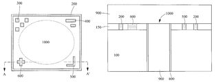
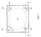
- FIG. 1 shows a schematic top view of an integrated structure with a through-silicon via (TSV) in accordance with an embodiment of the present invention
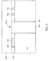
- FIG. 2 shows a schematic cross-sectional view of the integrated structure with a TSV taken along line A-A′ of FIG. 1 in accordance with an embodiment of the present invention
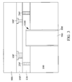
- FIG. 3 shows a schematic cross-sectional view of the integrated structure with a TSV taken along line A-A′ of FIG. 1 in accordance with another embodiment of the present invention.
- FIG. 1 shows a schematic top view of an integrated structure with a through-silicon via (TSV) 1000 in accordance with an embodiment of the present invention.
- TSV through-silicon via
- the TSV 1000 passes “through” a substrate 100 (not shown in FIG. 1 , please refer to FIG. 2-3 ) and physically and electrically connect the backside and front side of substrate 100 .
- the TSV 1000 is configured to couple operation voltage VSS, VDD or operational signal to the integrated circuits (not shown) formed on the substrate 100 .
- TSV 1000 Compared to normal active devices such as transistors, TSV 1000 has a much bigger size in a scale of micrometers. In one embodiment, TSV 1000 has a diameter of 30 ⁇ m. In another embodiment, TSV 1000 has a diameter of 10 ⁇ m. In a further embodiment, TSV 1000 has a diameter of 6 ⁇ m.
- a protective structure 200 is disposed to surround the TSV 1000 in order to isolate TSV 1000 physically and electrically from the active devices around it.
- the protective structure 200 shown in FIG. 1 has a rectangle or square shape. However, the protective structure 200 is not limited in its shape and how far it extends vertically as long as it is a closed structure surrounding the TSV within it.
- dummy patterns 200 and 300 with different shapes are introduced between the empty space between the protective structure 200 and the TSV 1000 .
- the size and shape of the dummy patterns 200 and 300 need not to be limited. Although only two kinds of dummy patterns (that is 200 and 300 ) are shown in FIG. 1 , more kinds of dummy patterns with different geometric features may be introduced as long as they can help to improve process uniformity and to relief mechanical stress caused by TSV 1000 .
- alignment marks 500 and 600 may be disposed around the TSV 1000 and the protective structure 200 to save space.
- the shapes, sizes and functions of these marks are not limited as long as they can perform the functions they supposed to perform.
- FIG. 2 shows a schematic cross-sectional view of the integrated structure with the TSV 1000 taken along line A-A′ of FIG. 1 in accordance with an embodiment of the present invention.
- a substrate 100 is provided. As shown in FIG. 2 , TSV 1000 penetrates the substrate 100 , couple the front side and backside of the substrate 100 and protrude from the front side.
- the substrate 100 can be a Si substrate, a polymer substrate, a silicon-on-insulator substrate, a SiC substrate, a composite substrate . . . etc.
- the backside is the side having no active devices such as transistors formed thereon.
- the backside of the substrate 100 is the opposite side of the front side of the substrate 100 , wherein active devices such as transistors and interconnect structures are formed on the front side.
- the TSV 1000 shown in FIG. 2-3 seems to be a TSV made from a via middle process, however TSV 1000 may be made from a via first process (via is made before transistors), a via middle process (via is made after transistors and during lower interconnects) or a via last process (via is made after interconnects).
- the basic structure of TSV 1000 is the same: a through-silicon hole, a dielectric layer 800 lining on the wall of the through-silicon hole, and a conductive material 900 filled in the through-silicon hole.
- the material/materials used for the dielectric layer 800 and the conductive material 900 may depend on the manufacturing process and the physical properties needed.
- Silicon oxide and/or silicon nitride are the most commonly used material/materials for the dielectric layer 800 .
- the conductive material 900 may comprise a barrier/glue layer material such as Ta, TaN, Ti, TiN, W, WN, Mo, Mn, Cu and a low-resistivity material such as W, Cu, Al, poly silicon.
- the dielectric layer 800 may rather be formed by thermal oxidation than deposition, then the dielectric layer 800 may not extend to the inter-layer dielectric layer 150 or the interconnect/device layer 130 .
- Inter-layer dielectric layer 150 may be a single-layered or multi-layered structure comprising one or more dielectric material selected from silicon dioxide, silicon nitride, SiC, SiON, SiCN, TEOS-based silicon dioxide, low-k dielectric materials . . . etc.
- the protective structure 200 and marks 500 and 600 are conductive contacts embedded in the inter-layer dielectric layer 150 . They can be made by the same single damascene processes. That is, they may be formed by forming one or more contact holes, forming one or more conductive materials on the substrate filling in the contact holes then performing a chemical mechanical polishing process to remove excess materials and form a global flat surface.
- the conductive materials used for the protective structure 200 and marks 500 and 600 comprise a barrier/glue material and a low-resistivity filling material.
- the barrier/glue material may be selected from Ta, TaN, Ti, TiN, W, WN, Mo, Mn, Cu, and the barrier/glue material preferably be Ta/TaN or Ti/TiN.
- the low-resistivity filling material may be selected from W, Cu, Al, poly silicon and the low-resistivity filling material preferably is W.
- dummy patterns 300 and 400 are also conductive contacts embedded in the inter-layer dielectric layer 150 . It appears from FIG.
- dummy patterns 300 and 400 , marks 500 and 600 are disposed at four different corners of the protective structure 200 , but the present invention is not limited. Different dummy patterns can be disposed at the same corner of the protective structure 200 and a plurality of marks of the same shape can be disposed at the same corner of the protective structure 200 .
- Interconnect layer 900 represents all the inter-metal dielectric layers and all the interconnect structures embedded within. It should be understood, FIG. 1-3 only show a part of a complete picture, therefore the substrate 100 may comprise shallow trench isolation structure and every kinds of doped regions while the inter-layer dielectric layer 150 may comprise active devices such as MOS transistors, passive devices such as resistors and other dummy patterns.
- FIG. 3 shows a schematic cross-sectional view of the integrated structure with TSV taken along line A-A′ of FIG. 1 in accordance with another embodiment of the present invention.
- dielectric layer 150 ′ corresponding to the dielectric layer 150 is not directly on the substrate 100 around TSV 1000 .
- the interconnect/device layer 130 may comprise one or more dielectric layers with interconnect structures embedded therein and/or active devices formed on substrate 100 .
- protective structure 200 ′ embedded in the interconnect/device layer 130 .
- the marks 500 ′ and 600 ′ in this embodiment corresponding to the marks 500 and 600 are made by dual damascene process instead of single damascene process. From this embodiment, it is clear that the protective structure 200 / 200 ′ should be at the same level (embedded in the same dielectric layer) with active devices so it can isolate the TSV 1000 from the active devices. The dummy patterns and the marks between the protective structure and TSV can be at different level (embedded in the different dielectric layer) from the protective structure.
- the substrate 100 may comprise shallow trench isolation structures right beneath the protective structure 200 / 200 ′, dummy patterns 300 and 400 , and marks 500 and 600 in order to isolate them from other functional active devices or routing interconnect.
- These shallow trench isolation structures may adapt different shapes and sizes to suit the protective structure 200 / 200 ′, dummy patterns 300 and 400 , and marks 500 and 600 .
- the present invention manages to isolate the TSV from the active devices in order to reduce the impacts caused by TSV on the active devices.
- the present invention also manages to make good use of the space around TSV and keep good process uniformity by adding marks and dummy patterns around TSV.
Landscapes
- Physics & Mathematics (AREA)
- Condensed Matter Physics & Semiconductors (AREA)
- General Physics & Mathematics (AREA)
- Engineering & Computer Science (AREA)
- Computer Hardware Design (AREA)
- Microelectronics & Electronic Packaging (AREA)
- Power Engineering (AREA)
- Internal Circuitry In Semiconductor Integrated Circuit Devices (AREA)
Abstract
Description
Claims (20)
Priority Applications (1)
| Application Number | Priority Date | Filing Date | Title |
|---|---|---|---|
| US13/833,786 US8957504B2 (en) | 2013-03-15 | 2013-03-15 | Integrated structure with a silicon-through via |
Applications Claiming Priority (1)
| Application Number | Priority Date | Filing Date | Title |
|---|---|---|---|
| US13/833,786 US8957504B2 (en) | 2013-03-15 | 2013-03-15 | Integrated structure with a silicon-through via |
Publications (2)
| Publication Number | Publication Date |
|---|---|
| US20140264916A1 US20140264916A1 (en) | 2014-09-18 |
| US8957504B2 true US8957504B2 (en) | 2015-02-17 |
Family
ID=51523941
Family Applications (1)
| Application Number | Title | Priority Date | Filing Date |
|---|---|---|---|
| US13/833,786 Expired - Fee Related US8957504B2 (en) | 2013-03-15 | 2013-03-15 | Integrated structure with a silicon-through via |
Country Status (1)
| Country | Link |
|---|---|
| US (1) | US8957504B2 (en) |
Cited By (6)
| Publication number | Priority date | Publication date | Assignee | Title |
|---|---|---|---|---|
| US20140239768A1 (en) * | 2013-02-27 | 2014-08-28 | Texas Instruments Incorporated | Capacitive micromachined ultrasonic transducer (cmut) with through-substrate via (tsv) substrate plug |
| US10075657B2 (en) | 2015-07-21 | 2018-09-11 | Fermi Research Alliance, Llc | Edgeless large area camera system |
| US10107830B2 (en) | 2013-02-27 | 2018-10-23 | Texas Instruments Incorporated | Method of forming capacitive MEMS sensor devices |
| US10352991B2 (en) | 2015-07-21 | 2019-07-16 | Fermi Research Alliance, Llc | Edgeless large area ASIC |
| US20220157737A1 (en) * | 2020-11-13 | 2022-05-19 | Samsung Electronics Co., Ltd. | Three dimensional integrated semiconductor architecture and method of manufacturing the same |
| US11749614B2 (en) | 2020-11-05 | 2023-09-05 | Samsung Electronics Co., Ltd. | Through-silicon via (TSV) key for overlay measurement, and semiconductor device and semiconductor package including TSV key |
Families Citing this family (5)
| Publication number | Priority date | Publication date | Assignee | Title |
|---|---|---|---|---|
| KR102177702B1 (en) | 2014-02-03 | 2020-11-11 | 삼성전자주식회사 | Via Structures and Semiconductor Devices Having a Via plug |
| US9425126B2 (en) * | 2014-05-29 | 2016-08-23 | Taiwan Semiconductor Manufacturing Company, Ltd. | Dummy structure for chip-on-wafer-on-substrate |
| US9397048B1 (en) * | 2015-03-23 | 2016-07-19 | Inotera Memories, Inc. | Semiconductor structure and manufacturing method thereof |
| US9997464B2 (en) * | 2016-04-29 | 2018-06-12 | Taiwan Semiconductor Manufacturing Company, Ltd. | Dummy features in redistribution layers (RDLS) and methods of forming same |
| JPWO2023058327A1 (en) * | 2021-10-08 | 2023-04-13 |
Citations (27)
| Publication number | Priority date | Publication date | Assignee | Title |
|---|---|---|---|---|
| US20100121994A1 (en) | 2008-11-10 | 2010-05-13 | International Business Machines Corporation | Stacked memory array |
| US7799678B2 (en) | 2008-01-30 | 2010-09-21 | Freescale Semiconductor, Inc. | Method for forming a through silicon via layout |
| US20100257495A1 (en) | 2009-04-06 | 2010-10-07 | Chan-Liang Wu | 3D-IC Verification Method |
| US20110147909A1 (en) | 2009-12-18 | 2011-06-23 | John Hsuan | Semicondcutor chip stack and manufacturing method thereof |
| US7969013B2 (en) * | 2009-10-22 | 2011-06-28 | Taiwan Semiconductor Manufacturing Company, Ltd. | Through silicon via with dummy structure and method for forming the same |
| US7989918B2 (en) | 2009-01-26 | 2011-08-02 | International Business Machines Corporation | Implementing tamper evident and resistant detection through modulation of capacitance |
| US8008195B2 (en) * | 2009-01-23 | 2011-08-30 | Oki Semiconductor Co., Ltd. | Method for manufacturing semiconductor device |
| US8103996B2 (en) | 2008-06-24 | 2012-01-24 | Cadence Design Systems, Inc. | Method and apparatus for thermal analysis of through-silicon via (TSV) |
| US8102064B2 (en) * | 2010-04-08 | 2012-01-24 | Nanya Technology Corp. | Electrical alignment mark set and method for aligning wafer stack |
| US8136084B2 (en) | 2009-09-09 | 2012-03-13 | International Business Machines Corporation | Arranging through silicon vias in IC layout |
| US8143704B2 (en) * | 2009-10-02 | 2012-03-27 | Texas Instruments Incorporated | Electronic assemblies including mechanically secured protruding bonding conductor joints |
| US20120106117A1 (en) | 2010-11-02 | 2012-05-03 | Georgia Tech Research Corporation | Ultra-thin interposer assemblies with through vias |
| US20120124532A1 (en) | 2010-11-11 | 2012-05-17 | International Business Machines Corporation | Implementing vertical die stacking to distribute logical function over multiple dies in through-silicon-via stacked semiconductor device |
| WO2012082092A1 (en) | 2010-12-13 | 2012-06-21 | Arm Limited | Inter-die connection within an integrated circuit formed of a stack of circuit dies |
| US8227889B2 (en) * | 2008-12-08 | 2012-07-24 | United Microelectronics Corp. | Semiconductor device |
| US20120273782A1 (en) | 2011-04-28 | 2012-11-01 | Taiwan Semiconductor Manufacturing Company, Ltd. | Interposers of 3-dimensional integrated circuit package systems and methods of designing the same |
| US8319336B2 (en) | 2010-07-08 | 2012-11-27 | Taiwan Semiconductor Manufacturing Company, Ltd. | Reduction of etch microloading for through silicon vias |
| US20120304142A1 (en) | 2010-12-09 | 2012-11-29 | Panasonic Corporation | Design support device of three-dimensional integrated circuit and method thereof |
| US8332803B1 (en) | 2010-06-28 | 2012-12-11 | Xilinx, Inc. | Method and apparatus for integrated circuit package thermo-mechanical reliability analysis |
| US20120331435A1 (en) | 2011-06-27 | 2012-12-27 | Xilinx, Inc. | Integrated circuit design using through silicon vias |
| US8344749B2 (en) | 2010-06-07 | 2013-01-01 | Texas Instruments Incorporated | Through carrier dual side loop-back testing of TSV die after die attach to substrate |
| US8350362B2 (en) * | 2010-05-28 | 2013-01-08 | Hynix Semiconductor Inc. | Semiconductor integrated circuit and method for fabricating the same |
| US8359554B2 (en) | 2008-06-18 | 2013-01-22 | Taiwan Semiconductor Manufacturing Company, Ltd. | Verification of 3D integrated circuits |
| US8362622B2 (en) | 2009-04-24 | 2013-01-29 | Synopsys, Inc. | Method and apparatus for placing transistors in proximity to through-silicon vias |
| US20130032799A1 (en) * | 2011-08-03 | 2013-02-07 | Taiwan Semiconductor Manufacturing Company, Ltd. | Apparatus and Methods for De-Embedding Through Substrate Vias |
| US20130134583A1 (en) * | 2011-05-26 | 2013-05-30 | Kabushiki Kaisha Toshiba | Semiconductor device and manufacturing method thereof |
| US20130341799A1 (en) * | 2012-06-21 | 2013-12-26 | Hsin-Yu Chen | Through silicon via structure and method of fabricating the same |
-
2013
- 2013-03-15 US US13/833,786 patent/US8957504B2/en not_active Expired - Fee Related
Patent Citations (27)
| Publication number | Priority date | Publication date | Assignee | Title |
|---|---|---|---|---|
| US7799678B2 (en) | 2008-01-30 | 2010-09-21 | Freescale Semiconductor, Inc. | Method for forming a through silicon via layout |
| US8359554B2 (en) | 2008-06-18 | 2013-01-22 | Taiwan Semiconductor Manufacturing Company, Ltd. | Verification of 3D integrated circuits |
| US8103996B2 (en) | 2008-06-24 | 2012-01-24 | Cadence Design Systems, Inc. | Method and apparatus for thermal analysis of through-silicon via (TSV) |
| US20100121994A1 (en) | 2008-11-10 | 2010-05-13 | International Business Machines Corporation | Stacked memory array |
| US8227889B2 (en) * | 2008-12-08 | 2012-07-24 | United Microelectronics Corp. | Semiconductor device |
| US8008195B2 (en) * | 2009-01-23 | 2011-08-30 | Oki Semiconductor Co., Ltd. | Method for manufacturing semiconductor device |
| US7989918B2 (en) | 2009-01-26 | 2011-08-02 | International Business Machines Corporation | Implementing tamper evident and resistant detection through modulation of capacitance |
| US20100257495A1 (en) | 2009-04-06 | 2010-10-07 | Chan-Liang Wu | 3D-IC Verification Method |
| US8362622B2 (en) | 2009-04-24 | 2013-01-29 | Synopsys, Inc. | Method and apparatus for placing transistors in proximity to through-silicon vias |
| US8136084B2 (en) | 2009-09-09 | 2012-03-13 | International Business Machines Corporation | Arranging through silicon vias in IC layout |
| US8143704B2 (en) * | 2009-10-02 | 2012-03-27 | Texas Instruments Incorporated | Electronic assemblies including mechanically secured protruding bonding conductor joints |
| US7969013B2 (en) * | 2009-10-22 | 2011-06-28 | Taiwan Semiconductor Manufacturing Company, Ltd. | Through silicon via with dummy structure and method for forming the same |
| US20110147909A1 (en) | 2009-12-18 | 2011-06-23 | John Hsuan | Semicondcutor chip stack and manufacturing method thereof |
| US8102064B2 (en) * | 2010-04-08 | 2012-01-24 | Nanya Technology Corp. | Electrical alignment mark set and method for aligning wafer stack |
| US8350362B2 (en) * | 2010-05-28 | 2013-01-08 | Hynix Semiconductor Inc. | Semiconductor integrated circuit and method for fabricating the same |
| US8344749B2 (en) | 2010-06-07 | 2013-01-01 | Texas Instruments Incorporated | Through carrier dual side loop-back testing of TSV die after die attach to substrate |
| US8332803B1 (en) | 2010-06-28 | 2012-12-11 | Xilinx, Inc. | Method and apparatus for integrated circuit package thermo-mechanical reliability analysis |
| US8319336B2 (en) | 2010-07-08 | 2012-11-27 | Taiwan Semiconductor Manufacturing Company, Ltd. | Reduction of etch microloading for through silicon vias |
| US20120106117A1 (en) | 2010-11-02 | 2012-05-03 | Georgia Tech Research Corporation | Ultra-thin interposer assemblies with through vias |
| US20120124532A1 (en) | 2010-11-11 | 2012-05-17 | International Business Machines Corporation | Implementing vertical die stacking to distribute logical function over multiple dies in through-silicon-via stacked semiconductor device |
| US20120304142A1 (en) | 2010-12-09 | 2012-11-29 | Panasonic Corporation | Design support device of three-dimensional integrated circuit and method thereof |
| WO2012082092A1 (en) | 2010-12-13 | 2012-06-21 | Arm Limited | Inter-die connection within an integrated circuit formed of a stack of circuit dies |
| US20120273782A1 (en) | 2011-04-28 | 2012-11-01 | Taiwan Semiconductor Manufacturing Company, Ltd. | Interposers of 3-dimensional integrated circuit package systems and methods of designing the same |
| US20130134583A1 (en) * | 2011-05-26 | 2013-05-30 | Kabushiki Kaisha Toshiba | Semiconductor device and manufacturing method thereof |
| US20120331435A1 (en) | 2011-06-27 | 2012-12-27 | Xilinx, Inc. | Integrated circuit design using through silicon vias |
| US20130032799A1 (en) * | 2011-08-03 | 2013-02-07 | Taiwan Semiconductor Manufacturing Company, Ltd. | Apparatus and Methods for De-Embedding Through Substrate Vias |
| US20130341799A1 (en) * | 2012-06-21 | 2013-12-26 | Hsin-Yu Chen | Through silicon via structure and method of fabricating the same |
Cited By (11)
| Publication number | Priority date | Publication date | Assignee | Title |
|---|---|---|---|---|
| US20140239768A1 (en) * | 2013-02-27 | 2014-08-28 | Texas Instruments Incorporated | Capacitive micromachined ultrasonic transducer (cmut) with through-substrate via (tsv) substrate plug |
| US9351081B2 (en) * | 2013-02-27 | 2016-05-24 | Texas Instruments Incorporated | Capacitive micromachined ultrasonic transducer (CMUT) with through-substrate via (TSV) substrate plug |
| US9937528B2 (en) | 2013-02-27 | 2018-04-10 | Texas Instruments Incorporated | Capacitive micromachined ultrasonic transducer (CMUT) forming |
| US10107830B2 (en) | 2013-02-27 | 2018-10-23 | Texas Instruments Incorporated | Method of forming capacitive MEMS sensor devices |
| US10075657B2 (en) | 2015-07-21 | 2018-09-11 | Fermi Research Alliance, Llc | Edgeless large area camera system |
| US10352991B2 (en) | 2015-07-21 | 2019-07-16 | Fermi Research Alliance, Llc | Edgeless large area ASIC |
| US11012642B2 (en) | 2015-07-21 | 2021-05-18 | Fermi Research Alliance, Llc | Edgeless large area camera system |
| US11749614B2 (en) | 2020-11-05 | 2023-09-05 | Samsung Electronics Co., Ltd. | Through-silicon via (TSV) key for overlay measurement, and semiconductor device and semiconductor package including TSV key |
| US20220157737A1 (en) * | 2020-11-13 | 2022-05-19 | Samsung Electronics Co., Ltd. | Three dimensional integrated semiconductor architecture and method of manufacturing the same |
| US11694968B2 (en) * | 2020-11-13 | 2023-07-04 | Samsung Electronics Co., Ltd | Three dimensional integrated semiconductor architecture having alignment marks provided in a carrier substrate |
| US12068256B2 (en) | 2020-11-13 | 2024-08-20 | Samsung Electronics Co., Ltd. | Method of manufacturing a three dimensional integrated semiconductor architecture having alignment marks provided in a carrier substrate |
Also Published As
| Publication number | Publication date |
|---|---|
| US20140264916A1 (en) | 2014-09-18 |
Similar Documents
| Publication | Publication Date | Title |
|---|---|---|
| US8957504B2 (en) | Integrated structure with a silicon-through via | |
| TWI754962B (en) | Semiconductor structure and method of fabricating the same | |
| JP6399887B2 (en) | Integrated circuit device having TSV structure and method of manufacturing the same | |
| US8884440B2 (en) | Integrated circuit device including through-silicon via structure having offset interface | |
| US10685907B2 (en) | Semiconductor structure with through silicon via and method for fabricating and testing the same | |
| US8987869B2 (en) | Integrated circuit devices including through-silicon-vias having integral contact pads | |
| CN106856194B (en) | Semiconductor chip and method of manufacturing the same | |
| US20120223440A1 (en) | Method of manufacturing three-dimensional integrated circuit and three-dimensional integrated circuit apparatus | |
| KR20170011366A (en) | Semiconductor chip and semiconductor package having same | |
| JP2015079960A (en) | Integrated circuit device and manufacturing method thereof | |
| JP2009277719A (en) | Semiconductor device and manufacturing method thereof | |
| US20140264917A1 (en) | A Semiconductor Device with a Through-Silicon Via and a Method for Making the Same | |
| TWI550749B (en) | Semiconductor wafer, semiconductor chip and semiconductor device and the fabricating method thereof | |
| US11749614B2 (en) | Through-silicon via (TSV) key for overlay measurement, and semiconductor device and semiconductor package including TSV key | |
| US20140264869A1 (en) | Semiconductor Device | |
| US8853090B1 (en) | Method for fabricating a through-silicon via | |
| US9030025B2 (en) | Integrated circuit layout | |
| CN104851875B (en) | Semiconductor structure with through silicon via and manufacturing method and testing method thereof | |
| US12489071B2 (en) | Semiconductor chip and semiconductor package including bonding layers having alignment marks | |
| CN104124228A (en) | Integrated structures with TSVs | |
| US11640950B2 (en) | Semiconductor chip and semiconductor package | |
| US8952500B2 (en) | Semiconductor device | |
| US20140264913A1 (en) | Semiconductor Device | |
| CN104124227A (en) | Semiconductor device | |
| KR100783276B1 (en) | Semiconductor device and manufacturing method |
Legal Events
| Date | Code | Title | Description |
|---|---|---|---|
| AS | Assignment |
Owner name: IPENVAL CONSULTANT INC., TAIWAN Free format text: ASSIGNMENT OF ASSIGNORS INTEREST;ASSIGNORS:HUANG, CHAO-YUAN;HO, YUEH-FENG;YANG, MING-SHENG;AND OTHERS;SIGNING DATES FROM 20130308 TO 20130315;REEL/FRAME:030011/0496 |
|
| FEPP | Fee payment procedure |
Free format text: MAINTENANCE FEE REMINDER MAILED (ORIGINAL EVENT CODE: REM.); ENTITY STATUS OF PATENT OWNER: SMALL ENTITY |
|
| LAPS | Lapse for failure to pay maintenance fees |
Free format text: PATENT EXPIRED FOR FAILURE TO PAY MAINTENANCE FEES (ORIGINAL EVENT CODE: EXP.); ENTITY STATUS OF PATENT OWNER: SMALL ENTITY |
|
| STCH | Information on status: patent discontinuation |
Free format text: PATENT EXPIRED DUE TO NONPAYMENT OF MAINTENANCE FEES UNDER 37 CFR 1.362 |
|
| FP | Lapsed due to failure to pay maintenance fee |
Effective date: 20190217 |