EP3925208B1 - Détecteur matriciel ayant un effet pair/impair réduit - Google Patents
Détecteur matriciel ayant un effet pair/impair réduit Download PDFInfo
- Publication number
- EP3925208B1 EP3925208B1 EP20702500.8A EP20702500A EP3925208B1 EP 3925208 B1 EP3925208 B1 EP 3925208B1 EP 20702500 A EP20702500 A EP 20702500A EP 3925208 B1 EP3925208 B1 EP 3925208B1
- Authority
- EP
- European Patent Office
- Prior art keywords
- transistor
- signal
- isolation
- gate
- matrix
- Prior art date
- Legal status (The legal status is an assumption and is not a legal conclusion. Google has not performed a legal analysis and makes no representation as to the accuracy of the status listed.)
- Active
Links
Images


Classifications
-
- G—PHYSICS
- G11—INFORMATION STORAGE
- G11C—STATIC STORES
- G11C19/00—Digital stores in which the information is moved stepwise, e.g. shift registers
- G11C19/28—Digital stores in which the information is moved stepwise, e.g. shift registers using semiconductor elements
-
- H—ELECTRICITY
- H04—ELECTRIC COMMUNICATION TECHNIQUE
- H04N—PICTORIAL COMMUNICATION, e.g. TELEVISION
- H04N25/00—Circuitry of solid-state image sensors [SSIS]; Control thereof
- H04N25/70—SSIS architectures; Circuits associated therewith
- H04N25/71—Charge-coupled device [CCD] sensors; Charge-transfer registers specially adapted for CCD sensors
- H04N25/745—Circuitry for generating timing or clock signals
-
- H—ELECTRICITY
- H04—ELECTRIC COMMUNICATION TECHNIQUE
- H04N—PICTORIAL COMMUNICATION, e.g. TELEVISION
- H04N25/00—Circuitry of solid-state image sensors [SSIS]; Control thereof
- H04N25/70—SSIS architectures; Circuits associated therewith
- H04N25/76—Addressed sensors, e.g. MOS or CMOS sensors
- H04N25/779—Circuitry for scanning or addressing the pixel array
-
- H—ELECTRICITY
- H04—ELECTRIC COMMUNICATION TECHNIQUE
- H04N—PICTORIAL COMMUNICATION, e.g. TELEVISION
- H04N25/00—Circuitry of solid-state image sensors [SSIS]; Control thereof
- H04N25/70—SSIS architectures; Circuits associated therewith
- H04N25/76—Addressed sensors, e.g. MOS or CMOS sensors
- H04N25/7795—Circuitry for generating timing or clock signals
Definitions
- the invention relates to a matrix detector, in which the effects of parasitic capacitances linked to different clock signals are reduced. It finds its application in particular for sensors capable of detecting a signal depending on a physical phenomenon, and in particular for image sensors.
- Matrix detectors are, in known manner, composed of pixels, formed at the intersection of rows and columns of a matrix.
- FIG 1 illustrates the arrangement in rows and columns of the pixels of a detector.
- Each pixel P(i,j) is composed of a light sensor D(i,j), generally a photodiode, which generates charges in proportion to the light energy received and stores them in its capacitance, and of a switching device T(i,j), whose source is connected to the load detector D(i,j).
- the switching device can be a thin film transistor T(i,j).
- Sequential addressing of lines L(i) requires supplying two distinct voltages: a voltage Voff to keep all the transistors T(i,j) of a line L(i) off and a voltage Von to turn on all the transistors T(i,j) of a line L(i).
- the transistors T(i,j) are addressed by a selection token (or "token" according to English terminology).
- the selection token is a high level signal (voltage Von) for a predetermined instant, compared to a low level (voltage Voff lower than Von), which propagates from line to line, in a given direction, for example from row L(i) to row L(i+1).
- the high level of the token controls the on state of all the transistors of the line.
- the high level of the select token is configured to have a value greater than the threshold voltage of the transistors.
- the electrons stored in each of the charge detectors D(i,j) of the row are transmitted to a charge integrator via the column Col(j) associated with the pixel P(i,j), which transforms this value into a voltage.
- Column Col(j) is connected to the source of transistor T(i,j).
- the integration of the loads in each column is managed by column addressers.
- the propagation of the selection token from line L(i) to the next line L(i+1) is managed by a line addressing device, or line scanner, commonly called “line driver”, or “gate”. driver”.
- the row addressing device is a shift register, comprising a plurality of stages. Each stage is connected to a row of the matrix.
- a signal generator which generates two clock signals out of phase with each other, is connected to the addressing device. At each clock stroke, the selection token propagates in the addressing device, passing from one stage to the next.
- the row addressing devices were initially arranged outside the matrix, connected to the matrix for example by flexible layers. More recently, row addressing devices have appeared implemented directly in the matrix, using single N or P type TFT transistors.
- the matrix can be produced by depositing layers on a substrate, for example of the amorphous silicon type ( a-Si), TFT, polysilicon, organic semiconductor, amorphous gallium indium zinc oxide (Ga 2 O 3 -In 2 O 3 -ZnO).
- GOA Gate driver On Array
- FIG 2 illustrates an electrical diagram representing two consecutive stages of a matrix addressing device.
- the two stages represented correspond to stages driven by two different clock signals, namely a first clock signal CK1, and a second clock signal CK2.
- a first clock signal CK1 a first clock signal
- a second clock signal CK2 a second clock signal
- an “odd stage” will be called a stage driven by the first clock signal CK1
- an “even stage” will be called a stage driven by the second clock signal CK2.
- FIG 2 therefore illustrates the electrical diagram of an odd stage and an even stage.
- Each stage is connected to a line comprising a plurality of pixels, as described above.
- Each stage comprises an output line restoring an activation signal as output (Out2n+1, Out2n+2).
- the stage includes an output transistor TFT4, which transmits a pulse of a clock signal at the output of the stage.
- the gate of output transistor TFT4 can be connected to an internal node NI of the stage, its source can be connected to output Out2n+1 and its drain can receive the signal from a first clock CK1.
- a boost capacitor C_SRFD can be connected between the gate and the source of the output transistor of the input stage TFT4.
- a first stage control transistor TFT1 (high leveling transistor, or “pull-up”) is capable of precharging the gate of output transistor TFT4. The source of the first control transistor TFT1 is thus connected to the gate of the output transistor TFT4.
- the gate and the drain of the first control transistor TFT1 are controlled by the output of the previous stage (stage 2n).
- the gate and the drain of the first control transistor TFT1 are controlled by the signal generator GSI, which generates a pulse STV.
- the GSI signal generator may comprise a dedicated circuit, for example an FPGA type circuit, coupled to a level converter.
- the FPGA receives control signals transmitted by a computing device (not shown).
- the FPGA generates logic signals at low voltage (for example between 0 and 3.3 V).
- the level converter ensures the compatibility between the low voltages of the FPGA, and the higher voltages of the matrix (Von, Voff).
- a second control transistor TFT3 is capable of discharging the gate of output transistor TFT4.
- the drain of the second control transistor TFT3 is thus connected to the gate of the output transistor TFT4.
- a discharge transistor TFT5 (low leveling transistor, or “pull-down”) can be connected to the output of the Out2n+1 stage.
- the gate of the discharge transistor TFT5 is connected to the gate of the second control transistor TFT3; it is also connected to the output signal Out2n+2 of the following stage.
- the document US 2013/0088265 A1 describes another example of GOA.
- the document FR 2 975 213 A1 describes a device for addressing the lines of an active detection matrix for imaging by ionizing radiation comprising a plurality of lines of pixels.
- the addressing device is made on a substrate on which the matrix is also made, and essentially comprises thin film transistors (TFT) of the single N or P type.
- TFT thin film transistors
- first signal CK1 and second signal CK2
- first signal CK1 and second signal CK2
- the voltage variation between the high level and the low level of the clock signals can reach several tens of volts. This sudden variation generates spurious signals, due to the capacitance of the gate, with peaks whose value can reach a few volts at the level of the output of the stage, at each rising edge and at each falling edge of the clock signal supplied to the floor (CK1 for odd floors, CK2 for even floors).
- the coupling caused by the first clock signal CK1 is found in all the lines connected to the first clock signal CK1. On a matrix detector of two thousand rows, during the integration of the charges at the level of each column, the coupling caused by the first clock signal CK1 is therefore multiplied by a thousand. The same applies to the coupling caused by the second clock signal CK2.
- the invention therefore aims to provide a matrix detector, making it possible to reduce the even/odd effect.
- the invention also aims to provide a matrix detector having reduced parasitic noise.
- the isolation circuit comprises an input terminal capable of receiving the intermediate output signal, an output terminal configured to deliver the selection signal, a first so-called isolation transistor, the gate of which is connected to the input terminal via a transistor mounted as a diode, the source of which is connected to the output terminal, and the drain of which is connected to receive the third clock signal, and a step-up capacitor, arranged between the gate and the source of the first isolation transistor.
- the isolation circuit comprises a second so-called isolation transistor, configured to isolate the output terminal with respect to the step-up capacitor when it is blocking.
- the isolation circuit comprises an impedance lowering circuit, connected between the gate of the first isolation transistor and the output terminal, and configured to maintain the potential of the line at the low level when the selection signal is at low level.
- each stage comprises a first reset transistor, configured to simultaneously deactivate the pixels of all the rows, and whose gate is controlled by a pulse of a reset signal supplied by the signal generator.
- each isolation circuit comprises a second reset transistor, configured to simultaneously activate the pixels of all the rows, and whose gate is controlled by the pulse of the reset signal, and whose source is capable of receiving a second control signal.
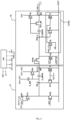
- FIG. 3 represents the electrical diagram of an AND stage of the addressing device, as described previously.
- the floor corresponds to a line L_n, it can be either an even line or an odd line.
- the drain of output transistor TFT4 receives a clock signal; by convention, it is defined that the output transistor TFT4 of an odd line receives, at its drain, the first clock signal CK1, and that the output transistor TFT4 of an even line receives, at its drain , the second clock signal CK2.
- a compensation capacitor C_SR can be arranged between the other clock signal (CK2 if the drain of output transistor TFT4 receives CK1, and vice versa) and the gate of output transistor TFT4.
- the compensation capacitor C_SR preferably has a value equivalent to that of the parasitic capacitance located between the gate and the drain of the output transistor TFT4.
- the compensation capacitor C_SR can be replaced by a transistor.
- the size of the transistor replacing the compensation capacitor C_SR is in this case equal to half that of the output transistor TFT4.
- the total capacitance is equivalent to the capacitance between the gate and the drain of the output transistor TFT4 (the TFTs being generally perfectly symmetrical).
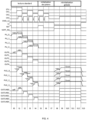
- FIG 4 represents a timing diagram, illustrating in particular the operation of the first four stages AND of the addressing device (under the “standard reading” column).
- PU_n is defined as being a first internal node of the AND stage, connected between the source of the first control transistor TFT1 and the gate of the output transistor TFT4.
- the signal PU_n corresponds to the voltage between the first internal node PU_n and the reference voltage Voff.
- BE input terminal
- the BE input terminal is configured to receive an intermediate output signal OUT_n.
- the intermediate output signal OUT_n can take a high level Von, which corresponds to a sufficient voltage to turn on the transistors of the pixels of the corresponding line, or a low level, to turn them off.
- the first control transistor of TFT1 of stage ET0 receives an input pulse STV (voltage Von), generated by a signal generator GSI.
- STV voltage Von
- the first control transistor of stage TFT1 is therefore on, and charges the boost capacitor C_SRFD.
- the potential of the first internal node PU_0 rises to the voltage Von, from which it is necessary to subtract the threshold voltage (V TFT1 ) of the first control transistor of the stage TFT1.
- the drain of output transistor TFT4 receives a clock pulse from the first clock signal CK1.
- the output transistor TFT4 is on.
- the first clock signal CK1 is at the high level Von
- the source of the output transistor TFT4 follows, driving the gate of the output transistor TFT4, which is floating, thanks to the raising capacitor C_SRFD.
- the voltage of the first internal node PU_0 changes to 2xVon
- the output transistor TFT4 is then largely on, and the intermediate output signal Out0 perfectly follows the first clock signal Ck1, until its descent at time t2.
- the first control transistor TFT1 of the next stage receives, at time t1, the intermediate output signal Out0 of the previous stage.
- the addressing device also includes an isolation circuit ISL.
- the isolation circuit ISL is connected between each stage AND and the corresponding line LI of the matrix.
- the isolation circuit ISL receives the intermediate output signal Outn, and a third clock signal CK3.
- the principle of the invention consists in applying the same clock signal CK3 to all the isolation circuits ISL connected to the rows of the matrix.
- the clock signal CK3 is a periodic signal, the high level of which is repeated on each passage to the high level of the first clock signal CK1 and of the second clock signal CK2.
- the isolation circuit ISL is configured to supply a selection signal OUT_LINE_n to the corresponding line L_n of the matrix.
- the selection signal OUT_LINE_n can pass from a high level (voltage Von) making it possible to select the pixels of the line, so that the detected charges are read, to a low level (voltage Voff).
- the selection signal OUT_LINE_n is delivered by an output terminal BS, connected to line L_n.
- the isolation circuit ISL comprises a first isolation transistor TFT6.
- the drain of the first isolation transistor TFT6 receives the third clock signal CK3.
- the first isolation transistor TFT6 thus makes it possible to pass the token transmitted by the AND stage when the third clock signal CK3 is at Von.
- a boost capacitor C_GDFD which makes it possible to obtain the “bootstrap” effect, is connected on the one hand to the gate of the first isolation transistor TFT6, and on the other hand to the output terminal BS.
- a diode-mounted transistor TFTD whose gate is connected to the source, is arranged between the input terminal BE and the gate of the first isolation transistor TFT6.
- the transistor mounted as a TFTD diode allows only positive voltages to pass.
- the second internal node PU2_n is the node located between the drain of the diode-mounted transistor TFTD and the gate of c.
- the isolation circuit is described in connection with the figure 4 .
- the intermediate output signal OUT_0 is at Von.
- the diode-mounted transistor TFTD is therefore on and charges the boost capacitor C_GDFD as long as the third clock signal CK3 is at Voff.
- the potential of the second internal node PU2_0 rises to the voltage Von, from which it is necessary to subtract the threshold voltage (V TFTD ) of the diode-mounted transistor TFTD.
- the first isolation transistor TFT6 is then slightly conducting.
- the charging of the second internal node PU2_0 to the precharge voltage Von-V TFTD turns on the first isolation transistor TFT6.
- the source of the first isolation transistor TFT6 follows, driving the gate of the first isolation transistor TFT6, which is floating, thanks to the step-up capacitor C_GDFD.
- the voltage of the second internal node PU2_0 goes to 2xVon, the first isolation transistor TFT6 is then largely conducting, and the selection signal OUT_LINE_0 passes to Von.
- the selection signal OUT_LINE_1 goes to Von, when the third clock signal CK3 is at Von.
- the duty cycle of the third clock signal CK3, namely the ratio, over a period, between the duration at Von and the duration at Voff, can be determined so that the time for the second internal node PU2_n to rise to Von, and by all the same putting the duration at Von as long as possible, because it is when it is when the third clock signal CK3 is at Von that the reading of the matrix is carried out.
- the duty cycle can therefore be determined as a function of the switching speed of the TFTs of the addressing device.
- the duty cycle can, for example, be determined by simulation, as a function of the values of the various components of the addressing device.
- the even/odd effect, present at the input terminal BE, is greatly reduced at the output terminal BS, thanks to the third clock signal CK3 which is common to all the rows of the matrix.
- a second isolation transistor TFT_RF is placed between the boost capacitor C_GDFD and the output terminal BS.
- the gate of the second isolation transistor TFT_RF is connected to the gate of the first isolation transistor TFT6.
- the second isolation transistor TFT_RF makes it possible to isolate the parasitic coupling still present in the elevation capacitor C_GDFD.
- the second isolation transistor TFT_RF and the first isolation transistor TFT6 are controlled by the same signal.
- the second isolation transistor TFT_RF is on when the token propagates in the isolation circuit ISL, and off the rest of the time.
- the second isolation transistor TFT_RF isolates the boost capacitor C_GDFD, except when the line needs to be on.
- the second isolation transistor TFT_RF also includes a parasitic capacitance, but its value is much lower than that of the boost capacitor C_GDFD.
- the isolation circuit ISL comprises an impedance lowering circuit LOWZ, connected between the gate of the first isolation transistor TFT6 and the output terminal BS.
- the impedance lowering circuit LOWZ makes it possible to maintain the potential of the line L_n at Voff when the selection signal OUT_LINE_n is at Voff. By keeping the line potential at Voff, when the token is not propagating through the stage, what remains of parasitic coupling is removed.
- the LOWZ impedance lowering circuit also makes it possible to prevent the transistors of the pixels from being permanently biased, which would have the consequence of accelerating their aging. It also makes it possible to avoid the appearance of parasitic tokens, caused by a drift of the transistors.
- the impedance lowering circuit LOWZ comprises a first impedance lowering circuit transistor TFT7, the drain of which is connected to the source of the first isolation transistor TFT6, the source of which is connected to the voltage Voff, and whose gate is connected to the gate of the first isolation transistor TFT6. It also includes a second transistor of the impedance lowering circuit TFT8, whose drain and gate are connected to the gate of the first isolation transistor TFT6, and whose source is connected to the voltage Voff. Finally, it comprises a third transistor of the impedance lowering circuit TFT9, controlled by a first control signal CMD_LZ supplied by the signal generator GSI, and whose drain is connected to the gate of the first isolation transistor TFT6.
- the second transistor of the impedance lowering circuit TFT8 switches on, and thus lets Voff pass.
- the first transistor of the impedance lowering circuit TFT7 therefore becomes off, so it no longer imposes Voff at the output terminal BS, so the token can pass, the line can be addressed.
- the second internal node PU2_n remains in the Voff state, the second transistor of the impedance lowering circuit TFT8 remains off and the gate of the first transistor of the circuit lowering impedance TFT7 remains at Von; it remains passing and imposes Voff on the line.
- the first control signal CMD_LZ allows the third transistor of the impedance lowering circuit TFT9 not to be permanently at Von.
- the control signal LZ which arrives at the source of the third transistor of the impedance lowering circuit TFT9, is indeed permanently at Von.
- the first control signal CMD_LZ can therefore have a duty cycle, preferably inverted with respect to that of the third clock signal CK3: it is mainly at Voff, except for a short time, during which it goes to Von, as well as illustrated in the timeline in figure 4 .
- the gate potential of the first transistor of the impedance lowering circuit TFT7 is therefore regularly reset (each time a line is addressed) to Von and ensures that the first transistor of the impedance lowering circuit TFT7 is on. as long as the second internal node PU2_n does not go to Von.
- the gate of the first transistor of the impedance lowering circuit TFT7 is not permanently maintained at Von thanks to the first control signal CMD_LZ; this allows the second transistor of the impedance lowering circuit TFT8 to easily switch the gate of the first transistor of the impedance lowering circuit TFT7 to Voff when the second internal node PU2_n is at Von. This also makes it possible to avoid possible short-circuits caused by an on state both of the second transistor of the impedance lowering circuit TFT8 and of the third transistor of the impedance lowering circuit TFT9.
- the matrix detector thus makes it possible to obtain a single and same parasitic effect for all the rows of the matrix, which can be corrected by known techniques, for example by carrying out, before the detection step, an image capture of white .
- each stage ET can also comprise a stage reset transistor TFT2 whose gate is controlled by a pulse of a reset signal RST.
- the source of the reset transistor TFT2 is connected to the source of the second control transistor TFT3 and to the source of the discharge transistor TFT5.
- the drain of the reset transistor TFT2 can be connected to the drain of the second input stage control transistor TFT3.
- each isolation circuit ISL comprises a second reset transistor TFT10, configured to simultaneously activate the pixels of all the rows.
- the gate of the second reset transistor TFT10 is controlled by the pulse of the reset signal RST, and the source is able to receive a second control signal Voff_RG.
- Voff_RG Voff which makes it possible to have a diagram equivalent to the previous one with the reset function unchanged.
- all the transistors of the isolation circuit ISL become blocking.
- Voff_RG Von
- RST Von
- LZ Voff.
- the AND stage is then reinitialized by the RST command, as indicated previously.
- the third clock signal CK3 is set to Von, to raise all the selection signals to Von.
- This global reset function is particularly advantageous in terms of power consumption.
- a sensor in a non-constant way, for example for fingerprint recognition on an electronic device, using the matrix detector, it is necessary to control the power consumed.
- the recognition function is used about 0.1% of the time at most. It is therefore necessary to turn off the reading electronics during idle times.
- Reading electronics can consume approximately 500 mW when taking an image, i.e. 135 mA under the 3.7 V of a telephone battery (of the "Smartphone” type), i.e. approximately 10% consumption of the battery if it does not is not extinguished.
- the global reset function made possible by the existence of a third clock signal CK3, makes it possible to keep the positive bias voltage to bias the photodiodes, and to perform a regular reset of the photodiodes in order to permanently keep a stable state.
Landscapes
- Engineering & Computer Science (AREA)
- Multimedia (AREA)
- Signal Processing (AREA)
- Shift Register Type Memory (AREA)
- Control Of Indicators Other Than Cathode Ray Tubes (AREA)
- Transforming Light Signals Into Electric Signals (AREA)
- Photometry And Measurement Of Optical Pulse Characteristics (AREA)
- Liquid Crystal Display Device Control (AREA)
Description
- L'invention se rapporte à un détecteur matriciel, dans lequel les effets des capacités parasites liés à des signaux d'horloges différents, sont réduits. Elle trouve son application notamment pour des capteurs apte à détecter un signal fonction d'un phénomène physique, et en particulier pour des capteurs d'images.
- Les détecteurs matriciels sont, de façon connue, composés de pixels, formés à l'intersection de lignes et de colonnes d'une matrice. La
figure 1 illustre l'agencement en lignes et en colonnes des pixels d'un détecteur. Chaque pixel P(i,j) est composée d'un capteur de lumière D(i,j), généralement une photodiode, qui génère des charges en proportion de l'énergie lumineuse reçue et les stocke dans sa capacité, et d'un dispositif de commutation T(i,j), dont la source est connectée au détecteur de charge D(i,j). En particulier, le dispositif de commutation peut être un transistor en couches minces T(i,j). - L'adressage séquentiel des lignes L(i) demande de fournir deux tensions distinctes : une tension Voff pour maintenir non passants tous les transistors T(i,j) d'une ligne L(i) et une tension Von pour rendre passant tous les transistors T(i,j) d'une ligne L(i). Les transistors T(i,j) sont adressés par un jeton de sélection (ou « token » selon la terminologie anglo-saxonne). Le jeton de sélection est un signal de niveau haut (tension Von) durant un instant prédéterminé, par rapport à un niveau bas (tension Voff inférieure à Von), qui se propage de ligne en ligne, dans un sens donné, par exemple de la ligne L(i) à la ligne L(i+1).
- Au moment où le jeton de sélection se propage dans une ligne L(i), le niveau haut du jeton commande l'état passant de tous les transistors de la ligne. Le niveau haut du jeton de sélection est configuré pour avoir une valeur supérieure à la tension de seuil des transistors. Les électrons stockés dans chacun des détecteurs de charge D(i,j) de la ligne sont transmis à un intégrateur de charge via la colonne Col(j) associée au pixel P(i,j), qui transforme cette valeur en tension. La colonne Col(j) est reliée à la source du transistor T(i,j). L'intégration des charges dans chaque colonne est gérée par des adresseurs de colonnes.
- La propagation du jeton de sélection de la ligne L(i) à la ligne suivante L(i+1) est gérée par un dispositif d'adressage de ligne, ou balayeur de lignes, appelé couramment « driver de ligne », ou « gate driver ». Le dispositif d'adressage de ligne est un registre à décalage, comprenant une pluralité d'étages. Chaque étage est connecté à une ligne de la matrice. Un générateur de signaux, qui génère deux signaux d'horloge déphasés l'un par rapport à l'autre, est connecté au dispositif d'adressage. A chaque coup d'horloge, le jeton de sélection se propage dans le dispositif d'adressage, en passant d'un étage au suivant.
- Les dispositifs d'adressage de ligne étaient initialement disposés en dehors de la matrice, reliés à la matrice par exemple par des nappes flexibles. Plus récemment sont apparus des dispositifs d'adressage de ligne implémentés directement dans la matrice, en utilisant des transistors TFT de type unique N ou P. La matrice peut être réalisée par un dépôt de couches sur un substrat, par exemple de type silicium amorphe (a-Si), TFT, silicium polycristallin, semiconducteur organique, oxyde de zinc Gallium Indium amorphe (Ga2O3-In2O3-ZnO).
- Ces dispositifs d'adressage intégrés dans la matrice, couramment appelés GOA (Gate driver On Array) permettent de gagner en coût de fabrication, en place occupée, et permet de limiter les erreurs de connexion par rapport aux dispositifs d'adressage externes.
- La
figure 2 illustre un schéma électrique représentant deux étages consécutifs d'un dispositif d'adressage de matrice. Les deux étages représentés correspondent à des étages pilotés par deux signaux d'horloge différents, à savoir un premier signal d'horloge CK1, et un deuxième signal d'horloge CK2. Par convention, on appellera, dans la présente demande, « étage impair » un étage piloté par le premier signal d'horloge CK1, et « étage pair » un étage piloté par le deuxième signal d'horloge CK2. Lafigure 2 illustre donc le schéma électrique d'un étage impair et d'un étage pair. Chaque étage est relié à une ligne comprenant une pluralité de pixels, comme décrit précédemment. - Chaque étage comprend une ligne de sortie restituant en sortie un signal d'activation (Out2n+1, Out2n+2). L'étage comprend un transistor de sortie TFT4, qui transmet une impulsion d'un signal d'horloge au niveau de la sortie de l'étage. La grille du transistor de sortie TFT4 peut être connectée à un noeud interne NI de l'étage, sa source peut être reliée à la sortie Out2n+1 et son drain peut recevoir le signal d'une première horloge CK1. Un condensateur d'élévation C_SRFD peut être connecté entre la grille et la source du transistor de sortie de l'étage d'entrée TFT4. Un premier transistor de commande de l'étage TFT1 (transistor de mise à niveau haut, ou « pull-up ») est apte à précharger la grille du transistor de sortie TFT4. La source du premier transistor de commande TFT1 est ainsi connectée à la grille du transistor de sortie TFT4. La grille et le drain du premier transistor de commande TFT1 sont commandés par la sortie de l'étage précédent (étage 2n). Pour le premier étage du dispositif d'adressage, la grille et le drain du premier transistor de commande TFT1 sont commandés par le générateur de signal GSI, qui génère une impulsion STV.
- Le générateur de signaux GSI peut comprendre un circuit dédié, par exemple un circuit de type FPGA, couplé à un convertisseur de niveau. Le FPGA reçoit des signaux de commande transmis par un dispositif de calcul (non représenté). Le FPGA génère les signaux logiques en faible tension (par exemple entre 0 et 3,3 V). Le convertisseur de niveau assure la compatibilité entre les faibles tensions du FPGA, et les tensions plus élevées de la matrice (Von, Voff).
- Un deuxième transistor de commande TFT3 est apte à décharger la grille du transistor de sortie TFT4. Le drain du deuxième transistor de commande TFT3 est ainsi connecté à la grille du transistor de sortie TFT4.
- Un transistor de décharge TFT5 (transistor de mise à niveau bas, ou « pull-down ») peut être connecté à la sortie de l'étage Out2n+1. La grille du transistor de décharge TFT5 est reliée à la grille du deuxième transistor de commande TFT3 ; elle est également reliée au signal de sortie Out2n+2 de l'étage suivant.
- La propagation du jeton s'effectue ainsi d'étage en étage, jusqu'à ce que toutes les lignes de la matrice aient été lues.
- Le document
US 2013/0088265 A1 décrit un autre exemple de GOA. Le documentFR 2 975 213 A1 - Le principe de l'adressage de lignes dans les afficheurs, et dans les détecteurs, est sensiblement le même. En effet, deux horloges différentes (premier signal CK1, et deuxième signal CK2) pilotent le transistor de sortie, en alternant d'un étage à l'autre. La variation de tension entre le niveau haut et le niveau bas des signaux d'horloge peut atteindre plusieurs dizaines de volts. Cette variation brutale engendre des signaux parasites, dus à la capacité de la grille, avec des pics dont la valeur peut atteindre quelques volts au niveau de la sortie de l'étage, à chaque front montant et à chaque front descendant du signal d'horloge fourni à l'étage (CK1 pour les étages impairs, CK2 pour les étages pairs).
- Ainsi, au niveau de chaque étage, même lorsque le jeton ne se propage pas dans l'étage (et donc avec un transistor de sortie TFT4 bloquant), un couplage parasite a lieu entre le signal d'horloge, qui arrive au niveau du drain du transistor de sortie TFT4, et la ligne menant aux pixels. De même, au niveau du transistor T(2n+1) du pixel P(2n+1), l'effet capacitif de la grille engendre des signaux parasites sur la colonne. Ces différents couplages parasites (horloge/ligne et ligne/colonne) sont matérialisés sur la
figure 2 , respectivement par les capacités Ca et Cb. - Le couplage provoqué par le premier signal d'horloge CK1 se retrouve dans toutes les lignes connectées au premier signal d'horloge CK1. Sur un détecteur matriciel de deux mille lignes, lors de l'intégration des charges au niveau de chaque colonne, le couplage provoqué par le premier signal d'horloge CK1 est donc multiplié par mille. Il en va de même du couplage provoqué par le deuxième signal d'horloge CK2.
- Dans le domaine des afficheurs, ces couplages parasites ne posent pas de difficultés, dans la mesure où une tension, correspondant au signal de données à afficher, est appliquée au niveau de chaque colonne. En revanche, dans le domaine des détecteurs, étant donné la faible quantité de charges du signal utile, les valeurs des couplages parasites peuvent largement dépasser la valeur des signaux à détecter. Typiquement, les valeurs des couplages parasites peuvent atteindre deux à trois cents fois la valeur du signal utile. La présence, sur une même colonne, de charges parasites ayant des valeurs différentes d'une ligne à l'autre, empêche d'effectuer un traitement correctif permettant de distinguer les charges parasites liées aux lignes paires, et les charges parasites liées au lignes impaires. Dans la présente demande, on appellera « effet pair/impair » le fait d'avoir, dans les colonnes, des signaux parasites issus de signaux d'horloges différents (certains signaux sur les lignes paires, d'autres sur les lignes impaires).
- L'invention vise donc à fournir un détecteur matriciel, permettant de réduire l'effet pair/impair. L'invention vise également à fournir un détecteur matriciel présentant un bruit parasite réduit.
- Un objet de l'invention est donc un détecteur matriciel comprenant :
- un ensemble de pixels organisés en matrice selon des lignes et des colonnes, chaque pixel étant adapté pour générer un signal fonction d'un phénomène physique,
- un générateur de signaux, configuré pour générer deux signaux d'horloges déphasés l'un par rapport à l'autre,
- un dispositif d'adressage des lignes comprenant un registre à décalage, le registre à décalage comprenant une pluralité d'étages disposés en cascade, chaque étage étant apte à recevoir, en alternance d'un étage à l'autre, un signal d'horloge parmi les deux signaux d'horloges, et étant apte à délivrer un signal de sortie intermédiaire pouvant prendre un niveau haut et un niveau bas, permettant respectivement d'activer et de désactiver les pixels de la ligne,
- Avantageusement, le circuit d'isolation comprend une borne d'entrée, apte à recevoir le signal de sortie intermédiaire, une borne de sortie, configuré pour délivrer le signal de sélection, un premier transistor dit d'isolation, dont la grille est connectée à la borne d'entrée par l'intermédiaire d'un transistor monté en diode, dont la source est connectée à la borne de sortie, et dont le drain est connecté pour recevoir le troisième signal d'horloge, et un condensateur d'élévation, disposé entre la grille et la source du premier transistor d'isolation.
- Avantageusement, le circuit d'isolation comprend un deuxième transistor dit d'isolation, configuré pour isoler la borne de sortie vis à vis du condensateur d'élévation lorsqu'il est bloquant.
- Avantageusement, le circuit d'isolation comprend un circuit d'abaissement d'impédance, connecté entre la grille du premier transistor d'isolation et la borne de sortie, et configuré pour maintenir le potentiel de la ligne au niveau bas lorsque signal de sélection est au niveau bas.
- Avantageusement, le circuit d'abaissement d'impédance comprend :
- un premier transistor du circuit d'abaissement d'impédance, dont le drain est relié à la source du premier transistor d'isolation, dont la source est reliée à une source de tension correspondant au niveau bas, et dont la grille est reliée à la grille du premier transistor d'isolation,
- un deuxième transistor du circuit d'abaissement d'impédance, dont le drain et la grille sont reliés à la grille du premier transistor d'isolation, et dont la source est reliée à la source de tension correspondant au niveau bas, et
- un troisième transistor du circuit d'abaissement d'impédance, commandé par un premier signal de commande fourni par le générateur de signaux, et dont le drain est relié à la grille du premier transistor d'isolation.
- Avantageusement, chaque étage comprend un premier transistor de réinitialisation, configuré pour désactiver simultanément les pixels de toutes les lignes, et dont la grille est commandée par une impulsion d'un signal de réinitialisation fourni par le générateur de signaux.
- Avantageusement, chaque circuit d'isolation comprend un deuxième transistor de réinitialisation, configuré pour activer simultanément les pixels de toutes les lignes, et dont la grille est commandée par l'impulsion du signal de réinitialisation, et dont la source est apte à recevoir un deuxième signal de commande.
- Les dessins annexés illustrent l'invention :
- [
Fig.1 ] Lafigure 1 , déjà décrite, représente l'agencement en lignes et en colonnes de pixels, selon l'état de la technique. - [
Fig.2 ] Lafigure 2 , déjà décrite, représente le schéma électrique de deux étages d'un registre à décalage, selon l'état de la technique. - [
Fig.3 ] Lafigure 3 , représente le schéma électrique d'un étage et d'un circuit d'isolation selon l'invention. - [
Fig.4 ] Lafigure 4 représente un diagramme des temps illustrant le fonctionnement du dispositif d'adressage de lignes selon l'invention. - La
figure 3 représente le schéma électrique d'un étage ET du dispositif d'adressage, tel que décrit précédemment. L'étage correspond à une ligne L_n, il peut s'agir indifféremment d'une ligne paire ou d'une ligne impaire. Le drain du transistor de sortie TFT4 reçoit un signal d'horloge ; par convention on définit que le transistor de sortie TFT4 d'une ligne impaire reçoit, au niveau de son drain, le premier signal d'horloge CK1, et que le transistor de sortie TFT4 d'une ligne paire reçoit, au niveau de son drain, le deuxième signal d'horloge CK2. - Un condensateur de compensation C_SR peut être disposé entre l'autre signal d'horloge (CK2 si le drain du transistor de sortie TFT4 reçoit CK1, et inversement) et la grille du transistor de sortie TFT4. Le condensateur de compensation C_SR a de préférence une valeur équivalente à celle de la capacité parasite située entre la grille et le drain du transistor de sortie TFT4. En variante, le condensateur de compensation C_SR peut être remplacé par un transistor. La taille du transistor remplaçant le condensateur de compensation C_SR est dans ce cas égale à la moitié de celle du transistor de sortie TFT4. Ainsi, la capacité totale est équivalente à la capacité entre la grille et le drain du transistor de sortie TFT4 (les TFT étant généralement parfaitement symétriques).
- La
figure 4 représente un diagramme des temps, illustrant notamment le fonctionnement des quatre premiers étages ET du dispositif d'adressage (sous la colonne « lecture standard »). - On définit PU_n comme étant un premier noeud interne de l'étage ET, connecté entre la source du premier transistor de commande TFT1 et la grille du transistor de sortie TFT4. Dans la
figure 4 , le signal PU_n correspond à la tension entre le premier noeud interne PU_n et la tension de référence Voff. On définit également une borne d'entrée BE, connecté entre la source du transistor de sortie TFT4 et le drain du transistor de décharge TFT5. La borne d'entrée BE est configurée pour recevoir un signal de sortie intermédiaire OUT_n. Le signal de sortie intermédiaire OUT_n peut prendre un niveau haut Von, qui correspond à une tension suffisante pour rendre passants les transistors des pixels de la ligne correspondante, ou un niveau bas, pour les rendre bloquants. - En référence à la
figure 4 , à l'instant t0, le premier transistor de commande de TFT1 de l'étage ET0 reçoit une impulsion d'entrée STV (tension Von), générée par un générateur de signaux GSI. Le premier transistor de commande de l'étage TFT1 est donc passant, et charge le condensateur d'élévation C_SRFD. Le potentiel du premier noeud interne PU_0 monte jusqu'à la tension Von, à laquelle il faut retrancher la tension de seuil (VTFT1) du premier transistor de commande de l'étage TFT1. - A l'instant t1, le drain du transistor de sortie TFT4 reçoit un coup d'horloge du premier signal d'horloge CK1. Comme le premier noeud interne PU_0 a été chargé au niveau de tension de précharge Von-VTFT1, le transistor de sortie TFT4 est passant. Le premier signal d'horloge CK1 est au niveau haut Von, la source du transistor de sortie TFT4 suit, entraînant la grille du transistor de sortie TFT4, qui est flottante, grâce au condensateur d'élévation C_SRFD. La tension du premier noeud interne PU_0 passe à 2xVon, le transistor de sortie TFT4 est alors largement passant, et le signal de sortie intermédiaire Out0 suit parfaitement le premier signal d'horloge Ck1, jusqu'à sa descente à l'instant t2. Le premier transistor de commande TFT1 de l'étage suivant reçoit, à l'instant t1, le signal de sortie intermédiaire Out0 de l'étage précédent.
- Le dispositif d'adressage comprend également un circuit d'isolation ISL. Le circuit d'isolation ISL est connecté entre chaque étage ET et la ligne LI correspondante de la matrice. Le circuit d'isolation ISL reçoit le signal de sortie intermédiaire Outn, et un troisième signal d'horloge CK3. Le principe de l'invention consiste à appliquer le même signal d'horloge CK3 sur tous les circuits d'isolation ISL connectés aux lignes de la matrice. Le signal d'horloge CK3 est un signal périodique, dont le niveau haut se répète à chaque passage au niveau haut du premier signal d'horloge CK1 et du deuxième signal d'horloge CK2.
- Le circuit d'isolation ISL est configuré pour fournir un signal de sélection OUT_LINE_n à la ligne L_n correspondante de la matrice. Le signal de sélection OUT_LINE_n peut passer d'un niveau haut (tension Von) permettant de sélectionner les pixels de la ligne, afin que les charges détectées soient lues, à un niveau bas (tension Voff). Le signal de sélection OUT_LINE_n est délivré par une borne de sortie BS, connectée à la ligne L_n.
- Le circuit d'isolation ISL comprend un premier transistor d'isolation TFT6. Le drain du premier transistor d'isolation TFT6 reçoit le troisième signal d'horloge CK3. Le premier transistor d'isolation TFT6 permet ainsi de faire passer le jeton transmis par l'étage ET lorsque le troisième signal d'horloge CK3 est à Von. Un condensateur d'élévation C_GDFD, qui permet d'obtenir l'effet « bootstrap », est relié d'une part à la grille du premier transistor d'isolation TFT6, et d'autre part à la borne de sortie BS. Par ailleurs, un transistor monté en diode TFTD, dont la grille est reliée à la source, est disposé entre la borne d'entrée BE et la grille du premier transistor d'isolation TFT6. Le transistor monté en diode TFTD permet de ne faire passer que les tensions positives. On appelle deuxième noeud interne PU2_n le noeud situé entre le drain du transistor monté en diode TFTD et la grille du c.
- Le fonctionnement du circuit d'isolation est décrit en lien avec la
figure 4 . A l'instant t1, le signal de sortie intermédiaire OUT_0 est à Von. Le transistor monté en diode TFTD est donc passant et charge le condensateur d'élévation C_GDFD tant que le troisième signal d'horloge CK3 est à Voff. Le potentiel du deuxième noeud interne PU2_0 monte jusqu'à la tension Von, à laquelle il faut retrancher la tension de seuil (VTFTD) du transistor monté en diode TFTD. Le premier transistor d'isolation TFT6 est alors légèrement passant. - Lorsque le troisième signal d'horloge CK3 passe à Von, le chargement du deuxième noeud interne PU2_0 à la tension de précharge Von-VTFTD rend passant le premier transistor d'isolation TFT6. La source du premier transistor d'isolation TFT6 suit, entraînant la grille du premier transistor d'isolation TFT6, qui est flottante, grâce au condensateur d'élévation C_GDFD. La tension du deuxième noeud interne PU2_0 passe à 2xVon, le premier transistor d'isolation TFT6 est alors largement passant, et le signal de sélection OUT_LINE_0 passe à Von.
- De la même manière, par propagation du jeton dans les étages successifs du registre à décalage, à l'instant t2, le signal de sélection OUT_LINE_1 passe à Von, lorsque le troisième signal d'horloge CK3 est à Von.
- Le rapport cyclique du troisième signal d'horloge CK3, à savoir le rapport, sur une période, entre la durée à Von et la durée à Voff, peut être déterminée de façon le temps au deuxième noeud interne PU2_n de monter à Von, et en mettant tout de même la durée à Von la plus longue possible, car c'est lorsque c'est lorsque le troisième signal d'horloge CK3 est à Von qu'est effectuée la lecture de la matrice. Le rapport cyclique peut donc être déterminé en fonction de la vitesse de commutation des TFT du dispositif d'adressage. Le rapport cyclique peut, par exemple, être déterminé par simulation, en fonction des valeurs des différents composants du dispositif d'adressage.
- L'effet pair/impair, présent au niveau de la borne d'entrée BE, est fortement réduit au niveau de la borne de sortie BS, grâce au troisième signal d'horloge CK3 qui est commun à toutes les lignes de la matrice.
- Selon un mode de réalisation particulièrement avantageux, un deuxième transistor d'isolation TFT_RF est disposé entre le condensateur d'élévation C_GDFD et la borne de sortie BS. La grille du deuxième transistor d'isolation TFT_RF est reliée à la grille du premier transistor d'isolation TFT6.
- Le deuxième transistor d'isolation TFT_RF permet d'isoler le couplage parasite encore présent dans le condensateur d'élévation C_GDFD. Le deuxième transistor d'isolation TFT_RF et le premier transistor d'isolation TFT6 sont commandés par le même signal. Ainsi, le deuxième transistor d'isolation TFT_RF est passant lorsque le jeton se propage dans le circuit d'isolation ISL, et bloquant le reste du temps. Le deuxième transistor d'isolation TFT_RF isole le condensateur d'élévation C_GDFD, sauf lorsque la ligne doit être activée. Le deuxième transistor d'isolation TFT_RF comprend également une capacité parasite, mais sa valeur est nettement inférieure à celle du condensateur d'élévation C_GDFD.
- Selon un autre mode de réalisation, le circuit d'isolation ISL comprend un circuit d'abaissement d'impédance LOWZ, connecté entre la grille du premier transistor d'isolation TFT6 et la borne de sortie BS. Le circuit d'abaissement d'impédance LOWZ permet de maintenir le potentiel de la ligne L_n à Voff lorsque signal de sélection OUT_LINE_n est à Voff. En maintenant le potentiel de la ligne à Voff, lorsque le jeton ne se propage pas dans l'étage, ce qu'il reste de couplage parasite est supprimé.
- Le circuit d'abaissement d'impédance LOWZ permet également d'éviter les que les transistors des pixels ne soient polarisés en permanence, ce qui aurait pour conséquence d'accélérer leur vieillissement. Il permet également d'éviter l'apparition de jetons parasites, provoqués par une dérive des transistors.
- Le circuit d'abaissement d'impédance LOWZ comprend un premier transistor du circuit d'abaissement d'impédance TFT7, dont le drain est relié à la source du premier transistor d'isolation TFT6, dont la source est reliée à la tension Voff, et dont la grille est reliée à la grille du premier transistor d'isolation TFT6. Il comprend également un deuxième transistor du circuit d'abaissement d'impédance TFT8, dont le drain et la grille sont reliés à la grille du premier transistor d'isolation TFT6, et dont la source est reliée à la tension Voff. Il comprend enfin un troisième transistor du circuit d'abaissement d'impédance TFT9, commandé par un premier signal de commande CMD_LZ fourni par le générateur de signaux GSI, et dont le drain est relié à la grille du premier transistor d'isolation TFT6.
- Lorsque le deuxième noeud interne PU2_n passe à Von, qui correspond à l'arrivée d'un jeton en provenance de l'étage ET, le deuxième transistor du circuit d'abaissement d'impédance TFT8 devient passant, et laisse ainsi passer Voff. Le premier transistor du circuit d'abaissement d'impédance TFT7 devient donc non passant, donc il n'impose plus Voff au niveau de la borne de sortie BS, donc le jeton peut passer, la ligne peut être adressée.
- En l'absence de jeton arrivant de l'étage ET, le deuxième noeud interne PU2_n reste à l'état Voff, le deuxième transistor du circuit d'abaissement d'impédance TFT8 reste non passant et la grille du premier transistor du circuit d'abaissement d'impédance TFT7 reste à Von ; celui-ci reste passant et impose Voff sur la ligne.
- Le premier signal de commande CMD_LZ permet au troisième transistor du circuit d'abaissement d'impédance TFT9 de ne pas être en permanence à Von. Le signal de commande LZ, qui arrive à la source du troisième transistor du circuit d'abaissement d'impédance TFT9, est en effet en permanence à Von. Le premier signal de commande CMD_LZ peut donc avoir un rapport cyclique, de préférence inversé par rapport à celui du troisième signal d'horloge CK3 : il est principalement à Voff, sauf pendant un court instant, durant lequel il passe à Von, ainsi qu'illustré dans le chronogramme en
figure 4 . - Le potentiel de grille du premier transistor du circuit d'abaissement d'impédance TFT7 est donc remis régulièrement (à chaque fois qu'une ligne est adressée) à Von et assure que le premier transistor du circuit d'abaissement d'impédance TFT7 soit passant tant que le deuxième noeud interne PU2_n ne passe pas à Von. La grille du premier transistor du circuit d'abaissement d'impédance TFT7 n'est pas maintenue en permanence à Von grâce au premier signal de commande CMD_LZ ; ceci permet que le deuxième transistor du circuit d'abaissement d'impédance TFT8 fasse passer facilement la grille du premier transistor du circuit d'abaissement d'impédance TFT7 à Voff lorsque le deuxième noeud interne PU2_n est à Von. Cela permet également d'éviter des éventuels court-circuits provoqués par un état passant à la fois du deuxième transistor du circuit d'abaissement d'impédance TFT8 et du troisième transistor du circuit d'abaissement d'impédance TFT9.
- Le détecteur matriciel permet ainsi d'obtenir un seul et même effet parasite pour toutes les lignes de la matrice, qui peut être corrigé par des techniques connues, par exemple en effectuant, avant l'étape de détection, une prise d'image de blanc.
- Avantageusement, chaque étage ET peut également comprendre un transistor de réinitialisation de l'étage TFT2 dont la grille est commandée par une impulsion d'un signal de réinitialisation RST. La source du transistor de réinitialisation TFT2 est connectée à la source du deuxième transistor de commande TFT3 et à la source du transistor de décharge TFT5. Le drain du transistor de réinitialisation TFT2 peut être connecté au drain du deuxième transistor de commande de l'étage d'entrée TFT3.
- En référence à la
figure 4 (sous la colonne « réinitialisation des jetons »), lorsqu'une impulsion du signal de réinitialisation RST est reçue au niveau de la grille du transistor de réinitialisation de l'étage TFT2. Ainsi, une impulsion de réinitialisation permet de rendre bloquant immédiatement les différents transistors compris dans l'étage ET. - Selon un mode de réalisation préférentiel, chaque circuit d'isolation ISL comprend un deuxième transistor de réinitialisation TFT10, configuré pour activer simultanément les pixels de toutes les lignes. La grille du deuxième transistor de réinitialisation TFT10 est commandée par l'impulsion du signal de réinitialisation RST, et la source est apte à recevoir un deuxième signal de commande Voff_RG.
- La
figure 4 (sous la colonne « réinitialisation globale ») permet de comprendre l'utilité du deuxième transistor de réinitialisation TFT10, commandé par un signal de commande. - En fonctionnement standard, Voff_RG = Voff ce qui permet d'avoir un schéma équivalent au précédent avec la fonction de reset inchangée. Ainsi, tous les transistors du circuit d'isolation ISL deviennent bloquants.
- Lorsqu'une réinitialisation globale doit être effectuée, on applique les commandes suivantes : Voff_RG=Von, RST = Von et LZ=Voff.
- L'étage ET est alors réinitialisé par la commande RST, comme indiqué précédemment. A t8, le deuxième noeud interne PU2_n monte à Von sur toutes les lignes en même temps (la commande LZ est désactivée, LZ = 0). Puis, à t9,le troisième signal d'horloge CK3 est mis à Von, pour monter tous les signaux de sélection à Von.
- Ensuite, en imposant Voff_RG = Voff et LZ = Von, à t13, tous les étages du GOA vont se remettre à Voff et l'électronique peut être éteinte.
- Cette fonction de réinitialisation globale est particulièrement avantageuse en termes de consommation de puissance. Lors de l'utilisation d'un capteur de manière non constante, par exemple pour de la reconnaissance d'empreinte digitale sur un appareil électronique, à l'aide du détecteur matriciel, il est nécessaire de contrôler la puissance consommée. Par exemple, la fonction de reconnaissance est utilisée environ 0.1% du temps au maximum. Il est donc nécessaire d'éteindre l'électronique de lecture pendant les temps morts.
- Une électronique de lecture peut consommer environ 500 mW lors de la prise d'image soit 135 mA sous les 3.7 V d'une batterie de téléphone (de type « Smartphone ») soit environ une consommation de 10% de la batterie si elle n'est pas éteinte.
- Or éteindre les alimentations d'une matrice de photodiode pendant un temps très long implique que le temps de réveil sera très long (quelques secondes) lié au fait que les photodiodes non polarisées se mettent dans un état très différent d'une photodiode polarisée et plusieurs dizaines images sont nécessaires pour stabiliser la matrice.
- La fonction de réinitialisation globale, rendue possible par l'existence d'un troisième signal d'horloge CK3, permet de conserver la tension de polarisation positive pour polariser les photodiodes, et de faire un une réinitialisation régulière des photodiodes afin de conserver en permanence un état stable.
Claims (5)
- Détecteur matriciel comprenant :- un ensemble de pixels organisés en matrice selon des lignes (L) et des colonnes, chaque pixel (P) étant adapté pour générer un signal fonction d'un phénomène physique,- un générateur de signaux (GSI), configuré pour générer deux signaux d'horloges (CK1, CK2) déphasés l'un par rapport à l'autre,- un dispositif d'adressage des lignes comprenant un registre à décalage (SR), le registre à décalage (SR) comprenant une pluralité d'étages (ET) disposés en cascade, chaque étage (ET) étant apte à recevoir, en alternance d'un étage à l'autre, un signal d'horloge parmi les deux signaux d'horloges (CK1, CK2), et étant apte à délivrer un signal de sortie intermédiaire (OUTn) pouvant prendre un niveau haut (Von) et un niveau bas (Voff), permettant respectivement d'activer et de désactiver les pixels de la ligne,le générateur de signaux (GSI) étant également configuré pour générer un troisième signal d'horloge (CK3), le dispositif d'adressage comprenant également une pluralité de circuit d'isolation (ISL), chaque circuit d'isolation (ISL) étant connecté entre chaque étage (ET) et la ligne (LI) correspondante de la matrice, et configuré pour recevoir le troisième signal d'horloge (CK3), le circuit d'isolation (ISL) étant configuré pour délivrer un signal de sélection (OUT_LINE n) de la ligne correspondante de la matrice lorsque le signal de sortie intermédiaire (OUTn) et le troisième signal d'horloge (CK3) sont au niveau haut (Von).dans lequel le circuit d'isolation (ISL) comprend une borne d'entrée (BE), apte à recevoir le signal de sortie intermédiaire (OUTn), une borne de sortie (BS), configuré pour délivrer le signal de sélection (OUT_LINE n), un premier transistor dit d'isolation (TFT6), dont la grille est connectée à la borne d'entrée (BE) par l'intermédiaire d'un transistor monté en diode (TFTD), dont la source est connectée à la borne de sortie (BS), et dont le drain est connecté pour recevoir le troisième signal d'horloge (CK3), et un condensateur d'élévation (C_GDFD), disposé entre la grille et la source du premier transistor d'isolation (TFT6),caractérisé en ce que le circuit d'isolation (ISL) comprend un deuxième transistor dit d'isolation (TFT_RF), configuré pour isoler la borne de sortie (BS) vis à vis du condensateur d'élévation (C_GDFD) lorsqu'il est bloquant.
- Détecteur matriciel selon la revendication 1, dans lequel le circuit d'isolation (ISL) comprend un circuit d'abaissement d'impédance (LOWZ), connecté entre la grille du premier transistor d'isolation (TFT6) et la borne de sortie (BS), et configuré pour maintenir le potentiel de la ligne (L) au niveau bas (Voff) lorsque signal de sélection (OUT_LINE_n) est au niveau bas (Voff).
- Détecteur matriciel selon la revendication 2, dans lequel le circuit d'abaissement d'impédance (LOWZ) comprend :- un premier transistor du circuit d'abaissement d'impédance (TFT7), dont le drain est relié à la source du premier transistor d'isolation (TFT6), dont la source est reliée à une source de tension (Voff) correspondant au niveau bas, et dont la grille est reliée à la grille du premier transistor d'isolation (TFT6),- un deuxième transistor du circuit d'abaissement d'impédance (TFT8), dont le drain et la grille sont reliés à la grille du premier transistor d'isolation (TFT6), et dont la source est reliée à la source de tension (Voff) correspondant au niveau bas, et- un troisième transistor du circuit d'abaissement d'impédance (TFT9), commandé par un premier signal de commande (CMD_LZ) fourni par le générateur de signaux (GSI), et dont le drain est relié à la grille du premier transistor d'isolation (TFT6).
- Détecteur matriciel selon la revendication 3, dans lequel chaque étage (ET) comprend un premier transistor de réinitialisation (TFT2), configuré pour désactiver simultanément les pixels de toutes les lignes, et dont la grille est commandée par une impulsion d'un signal de réinitialisation (RST) fourni par le générateur de signaux (GSI).
- Détecteur matriciel selon la revendication 4, dans lequel chaque circuit d'isolation (ISL) comprend un deuxième transistor de réinitialisation (TFT10), configuré pour activer simultanément les pixels de toutes les lignes, et dont la grille est commandée par l'impulsion du signal de réinitialisation (RST), et dont la source est apte à recevoir un deuxième signal de commande (VOFF_RG).
Applications Claiming Priority (2)
| Application Number | Priority Date | Filing Date | Title |
|---|---|---|---|
| FR1901328A FR3092721B1 (fr) | 2019-02-11 | 2019-02-11 | Détecteur matriciel ayant un effet pair/impair réduit |
| PCT/EP2020/053024 WO2020165024A1 (fr) | 2019-02-11 | 2020-02-06 | Détecteur matriciel ayant un effet pair/impair réduit |
Publications (2)
| Publication Number | Publication Date |
|---|---|
| EP3925208A1 EP3925208A1 (fr) | 2021-12-22 |
| EP3925208B1 true EP3925208B1 (fr) | 2023-04-05 |
Family
ID=67660187
Family Applications (1)
| Application Number | Title | Priority Date | Filing Date |
|---|---|---|---|
| EP20702500.8A Active EP3925208B1 (fr) | 2019-02-11 | 2020-02-06 | Détecteur matriciel ayant un effet pair/impair réduit |
Country Status (7)
| Country | Link |
|---|---|
| US (1) | US11882373B2 (fr) |
| EP (1) | EP3925208B1 (fr) |
| JP (1) | JP7457722B2 (fr) |
| CN (1) | CN113574859B (fr) |
| FR (1) | FR3092721B1 (fr) |
| TW (1) | TWI840504B (fr) |
| WO (1) | WO2020165024A1 (fr) |
Families Citing this family (2)
| Publication number | Priority date | Publication date | Assignee | Title |
|---|---|---|---|---|
| FR3114466B1 (fr) * | 2020-09-18 | 2024-12-13 | Trixell | Détecteur matriciel à plusieurs groupes de modules de pilotage et procédé de mise en œuvre du détecteur. |
| CN113744679B (zh) * | 2021-07-29 | 2024-02-09 | 北京大学深圳研究生院 | 一种栅极驱动电路及显示面板 |
Family Cites Families (20)
| Publication number | Priority date | Publication date | Assignee | Title |
|---|---|---|---|---|
| KR100281336B1 (ko) * | 1998-10-21 | 2001-03-02 | 구본준 | 쉬프트 레지스터 회로 |
| US7053945B1 (en) * | 2000-07-26 | 2006-05-30 | Micron Technolopgy, Inc. | Image sensor having boosted reset |
| KR100752602B1 (ko) * | 2001-02-13 | 2007-08-29 | 삼성전자주식회사 | 쉬프트 레지스터와, 이를 이용한 액정 표시 장치 |
| JP2004304331A (ja) | 2003-03-28 | 2004-10-28 | Matsushita Electric Ind Co Ltd | 固体撮像装置 |
| JP5132884B2 (ja) * | 2005-12-28 | 2013-01-30 | 三菱電機株式会社 | シフトレジスタ回路およびそれを備える画像表示装置 |
| JP5194494B2 (ja) * | 2007-03-12 | 2013-05-08 | コニカミノルタホールディングス株式会社 | 画素アレイ |
| JP5419762B2 (ja) * | 2010-03-18 | 2014-02-19 | 三菱電機株式会社 | シフトレジスタ回路 |
| JP5429815B2 (ja) * | 2010-04-05 | 2014-02-26 | 株式会社ジャパンディスプレイ | シフトレジスタ回路 |
| US8294077B2 (en) * | 2010-12-17 | 2012-10-23 | Omnivision Technologies, Inc. | Image sensor having supplemental capacitive coupling node |
| FR2975213B1 (fr) * | 2011-05-10 | 2013-05-10 | Trixell Sas | Dispositif d'adressage de lignes d'un circuit de commande pour matrice active de detection |
| CN102629444B (zh) | 2011-08-22 | 2014-06-25 | 北京京东方光电科技有限公司 | 栅极集成驱动电路、移位寄存器及显示屏 |
| JP5963551B2 (ja) | 2012-06-06 | 2016-08-03 | キヤノン株式会社 | アクティブマトリクスパネル、検出装置、及び、検出システム |
| US9466252B2 (en) * | 2013-09-10 | 2016-10-11 | Innolux Corporation | Partial scanning gate driver and liquid crystal display using the same |
| CN106710516A (zh) * | 2015-08-26 | 2017-05-24 | 上海和辉光电有限公司 | 显示装置、像素驱动电路及其驱动方法 |
| US9930280B2 (en) * | 2016-01-04 | 2018-03-27 | Sensors Unlimited, Inc. | Imaging pixel subarray with shared pulse detection |
| KR102607402B1 (ko) | 2016-10-31 | 2023-11-30 | 엘지디스플레이 주식회사 | 게이트 구동 회로와 이를 이용한 표시장치 |
| FR3064869B1 (fr) * | 2017-03-28 | 2019-05-03 | Commissariat A L'energie Atomique Et Aux Energies Alternatives | Capteur d'images |
| US9967504B1 (en) * | 2017-04-06 | 2018-05-08 | Omnivision Technologies, Inc. | Imaging sensor with boosted photodiode drive |
| CN108806611B (zh) * | 2018-06-28 | 2021-03-19 | 京东方科技集团股份有限公司 | 移位寄存器单元、栅极驱动电路、显示装置及驱动方法 |
| CN108682397A (zh) * | 2018-07-27 | 2018-10-19 | 京东方科技集团股份有限公司 | 移位寄存器单元、栅极驱动电路、显示装置以及驱动方法 |
-
2019
- 2019-02-11 FR FR1901328A patent/FR3092721B1/fr not_active Expired - Fee Related
-
2020
- 2020-02-06 EP EP20702500.8A patent/EP3925208B1/fr active Active
- 2020-02-06 US US17/429,903 patent/US11882373B2/en active Active
- 2020-02-06 WO PCT/EP2020/053024 patent/WO2020165024A1/fr not_active Ceased
- 2020-02-06 CN CN202080021523.8A patent/CN113574859B/zh active Active
- 2020-02-06 JP JP2021547126A patent/JP7457722B2/ja active Active
- 2020-02-10 TW TW109104076A patent/TWI840504B/zh active
Also Published As
| Publication number | Publication date |
|---|---|
| CN113574859A (zh) | 2021-10-29 |
| JP7457722B2 (ja) | 2024-03-28 |
| FR3092721A1 (fr) | 2020-08-14 |
| EP3925208A1 (fr) | 2021-12-22 |
| US20220191415A1 (en) | 2022-06-16 |
| US11882373B2 (en) | 2024-01-23 |
| WO2020165024A1 (fr) | 2020-08-20 |
| TW202040939A (zh) | 2020-11-01 |
| JP2022521169A (ja) | 2022-04-06 |
| FR3092721B1 (fr) | 2021-09-10 |
| CN113574859B (zh) | 2024-01-12 |
| TWI840504B (zh) | 2024-05-01 |
Similar Documents
| Publication | Publication Date | Title |
|---|---|---|
| US9123613B2 (en) | Image sensor and display | |
| EP2311042B1 (fr) | Registre a decalage a transistors a effet de champ | |
| WO1997025716A1 (fr) | Perfectionnement aux registres a decalage utilisant des transistors 'mis' de meme polarite | |
| EP2708023B1 (fr) | Dispositif d'adressage de lignes d'un circuit de commande pour matrice active de detection | |
| FR2720185A1 (fr) | Registre à décalage utilisant des transistors M.I.S. de même polarité. | |
| US8659576B2 (en) | Liquid crystal display with touch screen function and method for detecting external illuminance using the same | |
| JP3809750B2 (ja) | シフトレジスタ及び電子装置 | |
| TW200951933A (en) | Pixel circuit, display device having pixel circuit, and method of operating pixel circuit | |
| US9488521B2 (en) | Method for operating optical sensor circuit, and method for operating display apparatus provided with optical sensor circuit | |
| EP3924869B1 (fr) | Système d'acquisition d'empreinte digitale équipé d'un dispositif amélioré d'adressage de lignes | |
| JP4645047B2 (ja) | シフトレジスタ回路及びその駆動制御方法並びに駆動制御装置 | |
| WO2020165024A1 (fr) | Détecteur matriciel ayant un effet pair/impair réduit | |
| US7095005B2 (en) | Image reading device for reversing polarity of stored charge in capacitor | |
| JP2001176288A (ja) | シフトレジスタ及び電子装置 | |
| US8723096B2 (en) | Active photosensing pixel with two-terminal photosensing transistor | |
| US8717308B2 (en) | Display device with series connected optical sensors for determining touch position | |
| KR101278899B1 (ko) | 능동 감광 픽셀 | |
| KR20090071156A (ko) | 센싱 소자 및 센싱 방법 | |
| WO2021123123A1 (fr) | Procédé de commande d'un détecteur matriciel, et détecteur matriciel | |
| JP2008096242A (ja) | 光量検出装置およびそれを備えた液晶表示装置 | |
| FR2936087A1 (fr) | Registre a decalage a transistors a effet de champ. |
Legal Events
| Date | Code | Title | Description |
|---|---|---|---|
| STAA | Information on the status of an ep patent application or granted ep patent |
Free format text: STATUS: UNKNOWN |
|
| STAA | Information on the status of an ep patent application or granted ep patent |
Free format text: STATUS: THE INTERNATIONAL PUBLICATION HAS BEEN MADE |
|
| PUAI | Public reference made under article 153(3) epc to a published international application that has entered the european phase |
Free format text: ORIGINAL CODE: 0009012 |
|
| STAA | Information on the status of an ep patent application or granted ep patent |
Free format text: STATUS: REQUEST FOR EXAMINATION WAS MADE |
|
| 17P | Request for examination filed |
Effective date: 20210817 |
|
| AK | Designated contracting states |
Kind code of ref document: A1 Designated state(s): AL AT BE BG CH CY CZ DE DK EE ES FI FR GB GR HR HU IE IS IT LI LT LU LV MC MK MT NL NO PL PT RO RS SE SI SK SM TR |
|
| DAV | Request for validation of the european patent (deleted) | ||
| DAX | Request for extension of the european patent (deleted) | ||
| GRAP | Despatch of communication of intention to grant a patent |
Free format text: ORIGINAL CODE: EPIDOSNIGR1 |
|
| STAA | Information on the status of an ep patent application or granted ep patent |
Free format text: STATUS: GRANT OF PATENT IS INTENDED |
|
| INTG | Intention to grant announced |
Effective date: 20220908 |
|
| RIN1 | Information on inventor provided before grant (corrected) |
Inventor name: FEI, RICHUN Inventor name: BLANCHON, DAVID |
|
| GRAS | Grant fee paid |
Free format text: ORIGINAL CODE: EPIDOSNIGR3 |
|
| GRAA | (expected) grant |
Free format text: ORIGINAL CODE: 0009210 |
|
| STAA | Information on the status of an ep patent application or granted ep patent |
Free format text: STATUS: THE PATENT HAS BEEN GRANTED |
|
| AK | Designated contracting states |
Kind code of ref document: B1 Designated state(s): AL AT BE BG CH CY CZ DE DK EE ES FI FR GB GR HR HU IE IS IT LI LT LU LV MC MK MT NL NO PL PT RO RS SE SI SK SM TR |
|
| REG | Reference to a national code |
Ref country code: GB Ref legal event code: FG4D Free format text: NOT ENGLISH |
|
| REG | Reference to a national code |
Ref country code: DE Ref legal event code: R096 Ref document number: 602020009455 Country of ref document: DE |
|
| REG | Reference to a national code |
Ref country code: CH Ref legal event code: EP |
|
| REG | Reference to a national code |
Ref country code: AT Ref legal event code: REF Ref document number: 1559158 Country of ref document: AT Kind code of ref document: T Effective date: 20230415 |
|
| REG | Reference to a national code |
Ref country code: IE Ref legal event code: FG4D Free format text: LANGUAGE OF EP DOCUMENT: FRENCH |
|
| REG | Reference to a national code |
Ref country code: LT Ref legal event code: MG9D |
|
| P01 | Opt-out of the competence of the unified patent court (upc) registered |
Effective date: 20230621 |
|
| REG | Reference to a national code |
Ref country code: NL Ref legal event code: MP Effective date: 20230405 |
|
| REG | Reference to a national code |
Ref country code: AT Ref legal event code: MK05 Ref document number: 1559158 Country of ref document: AT Kind code of ref document: T Effective date: 20230405 |
|
| PG25 | Lapsed in a contracting state [announced via postgrant information from national office to epo] |
Ref country code: NL Free format text: LAPSE BECAUSE OF FAILURE TO SUBMIT A TRANSLATION OF THE DESCRIPTION OR TO PAY THE FEE WITHIN THE PRESCRIBED TIME-LIMIT Effective date: 20230405 |
|
| PG25 | Lapsed in a contracting state [announced via postgrant information from national office to epo] |
Ref country code: SE Free format text: LAPSE BECAUSE OF FAILURE TO SUBMIT A TRANSLATION OF THE DESCRIPTION OR TO PAY THE FEE WITHIN THE PRESCRIBED TIME-LIMIT Effective date: 20230405 Ref country code: PT Free format text: LAPSE BECAUSE OF FAILURE TO SUBMIT A TRANSLATION OF THE DESCRIPTION OR TO PAY THE FEE WITHIN THE PRESCRIBED TIME-LIMIT Effective date: 20230807 Ref country code: NO Free format text: LAPSE BECAUSE OF FAILURE TO SUBMIT A TRANSLATION OF THE DESCRIPTION OR TO PAY THE FEE WITHIN THE PRESCRIBED TIME-LIMIT Effective date: 20230705 Ref country code: ES Free format text: LAPSE BECAUSE OF FAILURE TO SUBMIT A TRANSLATION OF THE DESCRIPTION OR TO PAY THE FEE WITHIN THE PRESCRIBED TIME-LIMIT Effective date: 20230405 Ref country code: AT Free format text: LAPSE BECAUSE OF FAILURE TO SUBMIT A TRANSLATION OF THE DESCRIPTION OR TO PAY THE FEE WITHIN THE PRESCRIBED TIME-LIMIT Effective date: 20230405 |
|
| PG25 | Lapsed in a contracting state [announced via postgrant information from national office to epo] |
Ref country code: RS Free format text: LAPSE BECAUSE OF FAILURE TO SUBMIT A TRANSLATION OF THE DESCRIPTION OR TO PAY THE FEE WITHIN THE PRESCRIBED TIME-LIMIT Effective date: 20230405 Ref country code: PL Free format text: LAPSE BECAUSE OF FAILURE TO SUBMIT A TRANSLATION OF THE DESCRIPTION OR TO PAY THE FEE WITHIN THE PRESCRIBED TIME-LIMIT Effective date: 20230405 Ref country code: LV Free format text: LAPSE BECAUSE OF FAILURE TO SUBMIT A TRANSLATION OF THE DESCRIPTION OR TO PAY THE FEE WITHIN THE PRESCRIBED TIME-LIMIT Effective date: 20230405 Ref country code: LT Free format text: LAPSE BECAUSE OF FAILURE TO SUBMIT A TRANSLATION OF THE DESCRIPTION OR TO PAY THE FEE WITHIN THE PRESCRIBED TIME-LIMIT Effective date: 20230405 Ref country code: IS Free format text: LAPSE BECAUSE OF FAILURE TO SUBMIT A TRANSLATION OF THE DESCRIPTION OR TO PAY THE FEE WITHIN THE PRESCRIBED TIME-LIMIT Effective date: 20230805 Ref country code: HR Free format text: LAPSE BECAUSE OF FAILURE TO SUBMIT A TRANSLATION OF THE DESCRIPTION OR TO PAY THE FEE WITHIN THE PRESCRIBED TIME-LIMIT Effective date: 20230405 Ref country code: GR Free format text: LAPSE BECAUSE OF FAILURE TO SUBMIT A TRANSLATION OF THE DESCRIPTION OR TO PAY THE FEE WITHIN THE PRESCRIBED TIME-LIMIT Effective date: 20230706 Ref country code: AL Free format text: LAPSE BECAUSE OF FAILURE TO SUBMIT A TRANSLATION OF THE DESCRIPTION OR TO PAY THE FEE WITHIN THE PRESCRIBED TIME-LIMIT Effective date: 20230405 |
|
| PG25 | Lapsed in a contracting state [announced via postgrant information from national office to epo] |
Ref country code: FI Free format text: LAPSE BECAUSE OF FAILURE TO SUBMIT A TRANSLATION OF THE DESCRIPTION OR TO PAY THE FEE WITHIN THE PRESCRIBED TIME-LIMIT Effective date: 20230405 |
|
| REG | Reference to a national code |
Ref country code: DE Ref legal event code: R097 Ref document number: 602020009455 Country of ref document: DE |
|
| PG25 | Lapsed in a contracting state [announced via postgrant information from national office to epo] |
Ref country code: SK Free format text: LAPSE BECAUSE OF FAILURE TO SUBMIT A TRANSLATION OF THE DESCRIPTION OR TO PAY THE FEE WITHIN THE PRESCRIBED TIME-LIMIT Effective date: 20230405 |
|
| PG25 | Lapsed in a contracting state [announced via postgrant information from national office to epo] |
Ref country code: SM Free format text: LAPSE BECAUSE OF FAILURE TO SUBMIT A TRANSLATION OF THE DESCRIPTION OR TO PAY THE FEE WITHIN THE PRESCRIBED TIME-LIMIT Effective date: 20230405 Ref country code: SK Free format text: LAPSE BECAUSE OF FAILURE TO SUBMIT A TRANSLATION OF THE DESCRIPTION OR TO PAY THE FEE WITHIN THE PRESCRIBED TIME-LIMIT Effective date: 20230405 Ref country code: RO Free format text: LAPSE BECAUSE OF FAILURE TO SUBMIT A TRANSLATION OF THE DESCRIPTION OR TO PAY THE FEE WITHIN THE PRESCRIBED TIME-LIMIT Effective date: 20230405 Ref country code: EE Free format text: LAPSE BECAUSE OF FAILURE TO SUBMIT A TRANSLATION OF THE DESCRIPTION OR TO PAY THE FEE WITHIN THE PRESCRIBED TIME-LIMIT Effective date: 20230405 Ref country code: DK Free format text: LAPSE BECAUSE OF FAILURE TO SUBMIT A TRANSLATION OF THE DESCRIPTION OR TO PAY THE FEE WITHIN THE PRESCRIBED TIME-LIMIT Effective date: 20230405 Ref country code: CZ Free format text: LAPSE BECAUSE OF FAILURE TO SUBMIT A TRANSLATION OF THE DESCRIPTION OR TO PAY THE FEE WITHIN THE PRESCRIBED TIME-LIMIT Effective date: 20230405 |
|
| PLBE | No opposition filed within time limit |
Free format text: ORIGINAL CODE: 0009261 |
|
| STAA | Information on the status of an ep patent application or granted ep patent |
Free format text: STATUS: NO OPPOSITION FILED WITHIN TIME LIMIT |
|
| 26N | No opposition filed |
Effective date: 20240108 |
|
| PGFP | Annual fee paid to national office [announced via postgrant information from national office to epo] |
Ref country code: DE Payment date: 20240213 Year of fee payment: 5 Ref country code: GB Payment date: 20240221 Year of fee payment: 5 |
|
| PG25 | Lapsed in a contracting state [announced via postgrant information from national office to epo] |
Ref country code: SI Free format text: LAPSE BECAUSE OF FAILURE TO SUBMIT A TRANSLATION OF THE DESCRIPTION OR TO PAY THE FEE WITHIN THE PRESCRIBED TIME-LIMIT Effective date: 20230405 |
|
| PG25 | Lapsed in a contracting state [announced via postgrant information from national office to epo] |
Ref country code: SI Free format text: LAPSE BECAUSE OF FAILURE TO SUBMIT A TRANSLATION OF THE DESCRIPTION OR TO PAY THE FEE WITHIN THE PRESCRIBED TIME-LIMIT Effective date: 20230405 Ref country code: IT Free format text: LAPSE BECAUSE OF FAILURE TO SUBMIT A TRANSLATION OF THE DESCRIPTION OR TO PAY THE FEE WITHIN THE PRESCRIBED TIME-LIMIT Effective date: 20230405 |
|
| PG25 | Lapsed in a contracting state [announced via postgrant information from national office to epo] |
Ref country code: MC Free format text: LAPSE BECAUSE OF FAILURE TO SUBMIT A TRANSLATION OF THE DESCRIPTION OR TO PAY THE FEE WITHIN THE PRESCRIBED TIME-LIMIT Effective date: 20230405 |
|
| REG | Reference to a national code |
Ref country code: CH Ref legal event code: PL |
|
| PG25 | Lapsed in a contracting state [announced via postgrant information from national office to epo] |
Ref country code: LU Free format text: LAPSE BECAUSE OF NON-PAYMENT OF DUE FEES Effective date: 20240206 |
|
| PG25 | Lapsed in a contracting state [announced via postgrant information from national office to epo] |
Ref country code: CH Free format text: LAPSE BECAUSE OF NON-PAYMENT OF DUE FEES Effective date: 20240229 |
|
| PG25 | Lapsed in a contracting state [announced via postgrant information from national office to epo] |
Ref country code: LU Free format text: LAPSE BECAUSE OF NON-PAYMENT OF DUE FEES Effective date: 20240206 Ref country code: CH Free format text: LAPSE BECAUSE OF NON-PAYMENT OF DUE FEES Effective date: 20240229 |
|
| PG25 | Lapsed in a contracting state [announced via postgrant information from national office to epo] |
Ref country code: BG Free format text: LAPSE BECAUSE OF FAILURE TO SUBMIT A TRANSLATION OF THE DESCRIPTION OR TO PAY THE FEE WITHIN THE PRESCRIBED TIME-LIMIT Effective date: 20230405 |
|
| PG25 | Lapsed in a contracting state [announced via postgrant information from national office to epo] |
Ref country code: BG Free format text: LAPSE BECAUSE OF FAILURE TO SUBMIT A TRANSLATION OF THE DESCRIPTION OR TO PAY THE FEE WITHIN THE PRESCRIBED TIME-LIMIT Effective date: 20230405 |
|
| REG | Reference to a national code |
Ref country code: BE Ref legal event code: MM Effective date: 20240229 |
|
| PG25 | Lapsed in a contracting state [announced via postgrant information from national office to epo] |
Ref country code: BE Free format text: LAPSE BECAUSE OF NON-PAYMENT OF DUE FEES Effective date: 20240229 |
|
| PG25 | Lapsed in a contracting state [announced via postgrant information from national office to epo] |
Ref country code: IE Free format text: LAPSE BECAUSE OF NON-PAYMENT OF DUE FEES Effective date: 20240206 |
|
| PG25 | Lapsed in a contracting state [announced via postgrant information from national office to epo] |
Ref country code: IE Free format text: LAPSE BECAUSE OF NON-PAYMENT OF DUE FEES Effective date: 20240206 Ref country code: BE Free format text: LAPSE BECAUSE OF NON-PAYMENT OF DUE FEES Effective date: 20240229 |
|
| PG25 | Lapsed in a contracting state [announced via postgrant information from national office to epo] |
Ref country code: CY Free format text: LAPSE BECAUSE OF FAILURE TO SUBMIT A TRANSLATION OF THE DESCRIPTION OR TO PAY THE FEE WITHIN THE PRESCRIBED TIME-LIMIT; INVALID AB INITIO Effective date: 20200206 |
|
| REG | Reference to a national code |
Ref country code: DE Ref legal event code: R119 Ref document number: 602020009455 Country of ref document: DE |
|
| PG25 | Lapsed in a contracting state [announced via postgrant information from national office to epo] |
Ref country code: HU Free format text: LAPSE BECAUSE OF FAILURE TO SUBMIT A TRANSLATION OF THE DESCRIPTION OR TO PAY THE FEE WITHIN THE PRESCRIBED TIME-LIMIT; INVALID AB INITIO Effective date: 20200206 |
|
| PGFP | Annual fee paid to national office [announced via postgrant information from national office to epo] |
Ref country code: FR Payment date: 20250807 Year of fee payment: 6 |
|
| GBPC | Gb: european patent ceased through non-payment of renewal fee |
Effective date: 20250206 |
|
| PG25 | Lapsed in a contracting state [announced via postgrant information from national office to epo] |
Ref country code: TR Free format text: LAPSE BECAUSE OF FAILURE TO SUBMIT A TRANSLATION OF THE DESCRIPTION OR TO PAY THE FEE WITHIN THE PRESCRIBED TIME-LIMIT Effective date: 20230405 |
|
| PG25 | Lapsed in a contracting state [announced via postgrant information from national office to epo] |
Ref country code: DE Free format text: LAPSE BECAUSE OF NON-PAYMENT OF DUE FEES Effective date: 20250902 |
|
| PG25 | Lapsed in a contracting state [announced via postgrant information from national office to epo] |
Ref country code: GB Free format text: LAPSE BECAUSE OF NON-PAYMENT OF DUE FEES Effective date: 20250206 |