EP3875845B1 - Fahrzeuglampe und verfahren zur herstellung davon - Google Patents
Fahrzeuglampe und verfahren zur herstellung davon Download PDFInfo
- Publication number
- EP3875845B1 EP3875845B1 EP19877641.1A EP19877641A EP3875845B1 EP 3875845 B1 EP3875845 B1 EP 3875845B1 EP 19877641 A EP19877641 A EP 19877641A EP 3875845 B1 EP3875845 B1 EP 3875845B1
- Authority
- EP
- European Patent Office
- Prior art keywords
- color filter
- light
- vehicle lamp
- fluorescent film
- pdms
- Prior art date
- Legal status (The legal status is an assumption and is not a legal conclusion. Google has not performed a legal analysis and makes no representation as to the accuracy of the status listed.)
- Active
Links
Images

Classifications
-
- B—PERFORMING OPERATIONS; TRANSPORTING
- B60—VEHICLES IN GENERAL
- B60Q—ARRANGEMENT OF SIGNALLING OR LIGHTING DEVICES, THE MOUNTING OR SUPPORTING THEREOF OR CIRCUITS THEREFOR, FOR VEHICLES IN GENERAL
- B60Q1/00—Arrangement of optical signalling or lighting devices, the mounting or supporting thereof or circuits therefor
- B60Q1/02—Arrangement of optical signalling or lighting devices, the mounting or supporting thereof or circuits therefor the devices being primarily intended to illuminate the way ahead or to illuminate other areas of way or environments
- B60Q1/04—Arrangement of optical signalling or lighting devices, the mounting or supporting thereof or circuits therefor the devices being primarily intended to illuminate the way ahead or to illuminate other areas of way or environments the devices being headlights
- B60Q1/06—Arrangement of optical signalling or lighting devices, the mounting or supporting thereof or circuits therefor the devices being primarily intended to illuminate the way ahead or to illuminate other areas of way or environments the devices being headlights adjustable, e.g. remotely-controlled from inside vehicle
- B60Q1/08—Arrangement of optical signalling or lighting devices, the mounting or supporting thereof or circuits therefor the devices being primarily intended to illuminate the way ahead or to illuminate other areas of way or environments the devices being headlights adjustable, e.g. remotely-controlled from inside vehicle automatically
- B60Q1/085—Arrangement of optical signalling or lighting devices, the mounting or supporting thereof or circuits therefor the devices being primarily intended to illuminate the way ahead or to illuminate other areas of way or environments the devices being headlights adjustable, e.g. remotely-controlled from inside vehicle automatically due to special conditions, e.g. adverse weather, type of road, badly illuminated road signs or potential dangers
-
- B—PERFORMING OPERATIONS; TRANSPORTING
- B05—SPRAYING OR ATOMISING IN GENERAL; APPLYING FLUENT MATERIALS TO SURFACES, IN GENERAL
- B05D—PROCESSES FOR APPLYING FLUENT MATERIALS TO SURFACES, IN GENERAL
- B05D5/00—Processes for applying liquids or other fluent materials to surfaces to obtain special surface effects, finishes or structures
- B05D5/06—Processes for applying liquids or other fluent materials to surfaces to obtain special surface effects, finishes or structures to obtain multicolour or other optical effects
-
- B—PERFORMING OPERATIONS; TRANSPORTING
- B05—SPRAYING OR ATOMISING IN GENERAL; APPLYING FLUENT MATERIALS TO SURFACES, IN GENERAL
- B05D—PROCESSES FOR APPLYING FLUENT MATERIALS TO SURFACES, IN GENERAL
- B05D7/00—Processes, other than flocking, specially adapted for applying liquids or other fluent materials to particular surfaces or for applying particular liquids or other fluent materials
- B05D7/24—Processes, other than flocking, specially adapted for applying liquids or other fluent materials to particular surfaces or for applying particular liquids or other fluent materials for applying particular liquids or other fluent materials
-
- B—PERFORMING OPERATIONS; TRANSPORTING
- B60—VEHICLES IN GENERAL
- B60Q—ARRANGEMENT OF SIGNALLING OR LIGHTING DEVICES, THE MOUNTING OR SUPPORTING THEREOF OR CIRCUITS THEREFOR, FOR VEHICLES IN GENERAL
- B60Q1/00—Arrangement of optical signalling or lighting devices, the mounting or supporting thereof or circuits therefor
- B60Q1/0029—Spatial arrangement
- B60Q1/0041—Spatial arrangement of several lamps in relation to each other
-
- C—CHEMISTRY; METALLURGY
- C09—DYES; PAINTS; POLISHES; NATURAL RESINS; ADHESIVES; COMPOSITIONS NOT OTHERWISE PROVIDED FOR; APPLICATIONS OF MATERIALS NOT OTHERWISE PROVIDED FOR
- C09D—COATING COMPOSITIONS, e.g. PAINTS, VARNISHES OR LACQUERS; FILLING PASTES; CHEMICAL PAINT OR INK REMOVERS; INKS; CORRECTING FLUIDS; WOODSTAINS; PASTES OR SOLIDS FOR COLOURING OR PRINTING; USE OF MATERIALS THEREFOR
- C09D183/00—Coating compositions based on macromolecular compounds obtained by reactions forming in the main chain of the macromolecule a linkage containing silicon, with or without sulfur, nitrogen, oxygen, or carbon only; Coating compositions based on derivatives of such polymers
- C09D183/04—Polysiloxanes
-
- C—CHEMISTRY; METALLURGY
- C09—DYES; PAINTS; POLISHES; NATURAL RESINS; ADHESIVES; COMPOSITIONS NOT OTHERWISE PROVIDED FOR; APPLICATIONS OF MATERIALS NOT OTHERWISE PROVIDED FOR
- C09D—COATING COMPOSITIONS, e.g. PAINTS, VARNISHES OR LACQUERS; FILLING PASTES; CHEMICAL PAINT OR INK REMOVERS; INKS; CORRECTING FLUIDS; WOODSTAINS; PASTES OR SOLIDS FOR COLOURING OR PRINTING; USE OF MATERIALS THEREFOR
- C09D5/00—Coating compositions, e.g. paints, varnishes or lacquers, characterised by their physical nature or the effects produced; Filling pastes
-
- F—MECHANICAL ENGINEERING; LIGHTING; HEATING; WEAPONS; BLASTING
- F21—LIGHTING
- F21S—NON-PORTABLE LIGHTING DEVICES; SYSTEMS THEREOF; VEHICLE LIGHTING DEVICES SPECIALLY ADAPTED FOR VEHICLE EXTERIORS
- F21S41/00—Illuminating devices specially adapted for vehicle exteriors, e.g. headlamps
- F21S41/10—Illuminating devices specially adapted for vehicle exteriors, e.g. headlamps characterised by the light source
- F21S41/14—Illuminating devices specially adapted for vehicle exteriors, e.g. headlamps characterised by the light source characterised by the type of light source
- F21S41/141—Light emitting diodes [LED]
- F21S41/143—Light emitting diodes [LED] the main emission direction of the LED being parallel to the optical axis of the illuminating device
-
- F—MECHANICAL ENGINEERING; LIGHTING; HEATING; WEAPONS; BLASTING
- F21—LIGHTING
- F21S—NON-PORTABLE LIGHTING DEVICES; SYSTEMS THEREOF; VEHICLE LIGHTING DEVICES SPECIALLY ADAPTED FOR VEHICLE EXTERIORS
- F21S41/00—Illuminating devices specially adapted for vehicle exteriors, e.g. headlamps
- F21S41/20—Illuminating devices specially adapted for vehicle exteriors, e.g. headlamps characterised by refractors, transparent cover plates, light guides or filters
-
- G—PHYSICS
- G02—OPTICS
- G02B—OPTICAL ELEMENTS, SYSTEMS OR APPARATUS
- G02B1/00—Optical elements characterised by the material of which they are made; Optical coatings for optical elements
- G02B1/04—Optical elements characterised by the material of which they are made; Optical coatings for optical elements made of organic materials, e.g. plastics
-
- G—PHYSICS
- G02—OPTICS
- G02B—OPTICAL ELEMENTS, SYSTEMS OR APPARATUS
- G02B5/00—Optical elements other than lenses
- G02B5/02—Diffusing elements; Afocal elements
- G02B5/0273—Diffusing elements; Afocal elements characterized by the use
- G02B5/0278—Diffusing elements; Afocal elements characterized by the use used in transmission
-
- G—PHYSICS
- G02—OPTICS
- G02B—OPTICAL ELEMENTS, SYSTEMS OR APPARATUS
- G02B5/00—Optical elements other than lenses
- G02B5/20—Filters
-
- G—PHYSICS
- G02—OPTICS
- G02B—OPTICAL ELEMENTS, SYSTEMS OR APPARATUS
- G02B5/00—Optical elements other than lenses
- G02B5/20—Filters
- G02B5/201—Filters in the form of arrays
-
- G—PHYSICS
- G02—OPTICS
- G02B—OPTICAL ELEMENTS, SYSTEMS OR APPARATUS
- G02B5/00—Optical elements other than lenses
- G02B5/20—Filters
- G02B5/22—Absorbing filters
- G02B5/223—Absorbing filters containing organic substances, e.g. dyes, inks or pigments
-
- H—ELECTRICITY
- H05—ELECTRIC TECHNIQUES NOT OTHERWISE PROVIDED FOR
- H05K—PRINTED CIRCUITS; CASINGS OR CONSTRUCTIONAL DETAILS OF ELECTRIC APPARATUS; MANUFACTURE OF ASSEMBLAGES OF ELECTRICAL COMPONENTS
- H05K1/00—Printed circuits
- H05K1/02—Details
- H05K1/03—Use of materials for the substrate
-
- H—ELECTRICITY
- H10—SEMICONDUCTOR DEVICES; ELECTRIC SOLID-STATE DEVICES NOT OTHERWISE PROVIDED FOR
- H10H—INORGANIC LIGHT-EMITTING SEMICONDUCTOR DEVICES HAVING POTENTIAL BARRIERS
- H10H20/00—Individual inorganic light-emitting semiconductor devices having potential barriers, e.g. light-emitting diodes [LED]
- H10H20/80—Constructional details
- H10H20/84—Coatings, e.g. passivation layers or antireflective coatings
-
- H—ELECTRICITY
- H10—SEMICONDUCTOR DEVICES; ELECTRIC SOLID-STATE DEVICES NOT OTHERWISE PROVIDED FOR
- H10H—INORGANIC LIGHT-EMITTING SEMICONDUCTOR DEVICES HAVING POTENTIAL BARRIERS
- H10H20/00—Individual inorganic light-emitting semiconductor devices having potential barriers, e.g. light-emitting diodes [LED]
- H10H20/80—Constructional details
- H10H20/85—Packages
- H10H20/851—Wavelength conversion means
- H10H20/8511—Wavelength conversion means characterised by their material, e.g. binder
-
- H—ELECTRICITY
- H10—SEMICONDUCTOR DEVICES; ELECTRIC SOLID-STATE DEVICES NOT OTHERWISE PROVIDED FOR
- H10H—INORGANIC LIGHT-EMITTING SEMICONDUCTOR DEVICES HAVING POTENTIAL BARRIERS
- H10H20/00—Individual inorganic light-emitting semiconductor devices having potential barriers, e.g. light-emitting diodes [LED]
- H10H20/80—Constructional details
- H10H20/85—Packages
- H10H20/851—Wavelength conversion means
- H10H20/8511—Wavelength conversion means characterised by their material, e.g. binder
- H10H20/8512—Wavelength conversion materials
-
- H—ELECTRICITY
- H10—SEMICONDUCTOR DEVICES; ELECTRIC SOLID-STATE DEVICES NOT OTHERWISE PROVIDED FOR
- H10H—INORGANIC LIGHT-EMITTING SEMICONDUCTOR DEVICES HAVING POTENTIAL BARRIERS
- H10H20/00—Individual inorganic light-emitting semiconductor devices having potential barriers, e.g. light-emitting diodes [LED]
- H10H20/80—Constructional details
- H10H20/85—Packages
- H10H20/855—Optical field-shaping means, e.g. lenses
-
- B—PERFORMING OPERATIONS; TRANSPORTING
- B05—SPRAYING OR ATOMISING IN GENERAL; APPLYING FLUENT MATERIALS TO SURFACES, IN GENERAL
- B05D—PROCESSES FOR APPLYING FLUENT MATERIALS TO SURFACES, IN GENERAL
- B05D1/00—Processes for applying liquids or other fluent materials
- B05D1/26—Processes for applying liquids or other fluent materials performed by applying the liquid or other fluent material from an outlet device in contact with, or almost in contact with, the surface
-
- B—PERFORMING OPERATIONS; TRANSPORTING
- B05—SPRAYING OR ATOMISING IN GENERAL; APPLYING FLUENT MATERIALS TO SURFACES, IN GENERAL
- B05D—PROCESSES FOR APPLYING FLUENT MATERIALS TO SURFACES, IN GENERAL
- B05D2201/00—Polymeric substrate or laminate
- B05D2201/02—Polymeric substrate
-
- B—PERFORMING OPERATIONS; TRANSPORTING
- B05—SPRAYING OR ATOMISING IN GENERAL; APPLYING FLUENT MATERIALS TO SURFACES, IN GENERAL
- B05D—PROCESSES FOR APPLYING FLUENT MATERIALS TO SURFACES, IN GENERAL
- B05D2518/00—Other type of polymers
- B05D2518/10—Silicon-containing polymers
- B05D2518/12—Ceramic precursors (polysiloxanes, polysilazanes)
-
- B—PERFORMING OPERATIONS; TRANSPORTING
- B05—SPRAYING OR ATOMISING IN GENERAL; APPLYING FLUENT MATERIALS TO SURFACES, IN GENERAL
- B05D—PROCESSES FOR APPLYING FLUENT MATERIALS TO SURFACES, IN GENERAL
- B05D3/00—Pretreatment of surfaces to which liquids or other fluent materials are to be applied; After-treatment of applied coatings, e.g. intermediate treating of an applied coating preparatory to subsequent applications of liquids or other fluent materials
- B05D3/02—Pretreatment of surfaces to which liquids or other fluent materials are to be applied; After-treatment of applied coatings, e.g. intermediate treating of an applied coating preparatory to subsequent applications of liquids or other fluent materials by baking
- B05D3/0254—After-treatment
- B05D3/0272—After-treatment with ovens
-
- B—PERFORMING OPERATIONS; TRANSPORTING
- B05—SPRAYING OR ATOMISING IN GENERAL; APPLYING FLUENT MATERIALS TO SURFACES, IN GENERAL
- B05D—PROCESSES FOR APPLYING FLUENT MATERIALS TO SURFACES, IN GENERAL
- B05D7/00—Processes, other than flocking, specially adapted for applying liquids or other fluent materials to particular surfaces or for applying particular liquids or other fluent materials
- B05D7/50—Multilayers
- B05D7/56—Three layers or more
- B05D7/57—Three layers or more the last layer being a clear coat
- B05D7/576—Three layers or more the last layer being a clear coat each layer being cured, at least partially, separately
-
- C—CHEMISTRY; METALLURGY
- C08—ORGANIC MACROMOLECULAR COMPOUNDS; THEIR PREPARATION OR CHEMICAL WORKING-UP; COMPOSITIONS BASED THEREON
- C08G—MACROMOLECULAR COMPOUNDS OBTAINED OTHERWISE THAN BY REACTIONS ONLY INVOLVING UNSATURATED CARBON-TO-CARBON BONDS
- C08G77/00—Macromolecular compounds obtained by reactions forming a linkage containing silicon with or without sulfur, nitrogen, oxygen or carbon in the main chain of the macromolecule
- C08G77/04—Polysiloxanes
-
- F—MECHANICAL ENGINEERING; LIGHTING; HEATING; WEAPONS; BLASTING
- F21—LIGHTING
- F21S—NON-PORTABLE LIGHTING DEVICES; SYSTEMS THEREOF; VEHICLE LIGHTING DEVICES SPECIALLY ADAPTED FOR VEHICLE EXTERIORS
- F21S41/00—Illuminating devices specially adapted for vehicle exteriors, e.g. headlamps
- F21S41/10—Illuminating devices specially adapted for vehicle exteriors, e.g. headlamps characterised by the light source
- F21S41/14—Illuminating devices specially adapted for vehicle exteriors, e.g. headlamps characterised by the light source characterised by the type of light source
- F21S41/141—Light emitting diodes [LED]
-
- H—ELECTRICITY
- H10—SEMICONDUCTOR DEVICES; ELECTRIC SOLID-STATE DEVICES NOT OTHERWISE PROVIDED FOR
- H10H—INORGANIC LIGHT-EMITTING SEMICONDUCTOR DEVICES HAVING POTENTIAL BARRIERS
- H10H20/00—Individual inorganic light-emitting semiconductor devices having potential barriers, e.g. light-emitting diodes [LED]
- H10H20/01—Manufacture or treatment
- H10H20/034—Manufacture or treatment of coatings
-
- H—ELECTRICITY
- H10—SEMICONDUCTOR DEVICES; ELECTRIC SOLID-STATE DEVICES NOT OTHERWISE PROVIDED FOR
- H10H—INORGANIC LIGHT-EMITTING SEMICONDUCTOR DEVICES HAVING POTENTIAL BARRIERS
- H10H20/00—Individual inorganic light-emitting semiconductor devices having potential barriers, e.g. light-emitting diodes [LED]
- H10H20/01—Manufacture or treatment
- H10H20/036—Manufacture or treatment of packages
- H10H20/0361—Manufacture or treatment of packages of wavelength conversion means
-
- H—ELECTRICITY
- H10—SEMICONDUCTOR DEVICES; ELECTRIC SOLID-STATE DEVICES NOT OTHERWISE PROVIDED FOR
- H10H—INORGANIC LIGHT-EMITTING SEMICONDUCTOR DEVICES HAVING POTENTIAL BARRIERS
- H10H20/00—Individual inorganic light-emitting semiconductor devices having potential barriers, e.g. light-emitting diodes [LED]
- H10H20/01—Manufacture or treatment
- H10H20/036—Manufacture or treatment of packages
- H10H20/0363—Manufacture or treatment of packages of optical field-shaping means
-
- H—ELECTRICITY
- H10—SEMICONDUCTOR DEVICES; ELECTRIC SOLID-STATE DEVICES NOT OTHERWISE PROVIDED FOR
- H10H—INORGANIC LIGHT-EMITTING SEMICONDUCTOR DEVICES HAVING POTENTIAL BARRIERS
- H10H20/00—Individual inorganic light-emitting semiconductor devices having potential barriers, e.g. light-emitting diodes [LED]
- H10H20/80—Constructional details
- H10H20/882—Scattering means
Definitions
- the present application relates to a vehicle lamp and a method for manufacturing the same.
- Vehicles comprise a variety of vehicle lamps performing illumination or signaling functions.
- halogen lamps or gas discharge lamps have been mainly used, but in recent years, light-emitting diodes (LEDs) have attracted attention as light sources for vehicle lamps.
- JP2018049971A discloses the manufacturing of a LED used in a vehicle-mounted lamp.
- a fluorecsent pigment may be used in the structure.
- a light-emitting diode which is not in the form of a package, is a semiconductor light-emitting device that converts current to light and is continually being developed as a light source for display images of electronic devices comprising information communication devices.
- the upper substrate usually comprises a light-diffusing layer/fluorescent layer/color filter layer.
- the light-diffusing layer and the fluorescent layer use PDMS as a material and the color filter layer uses a dispersed pigment to minimize the loss of luminance.
- a comma coater capable of coating the light-diffusing layer and the fluorescent layer cannot be used due to the low viscosity resulting from the presence of the solvent for dispersion.
- other types of coaters such as slot dies are inevitably used, and the curing time is lengthened, thus resulting in problems such as increased processing costs and time delays.
- the light-diffusing layer, the fluorescent layer and the color filter layer contain different kinds of binders, thus disadvantageously resulting in a high possibility of deformation such as warping or twisting.
- the present application is directed to providing a vehicle lamp and a method for manufacturing the same.
- One embodiment of the present application provides a vehicle lamp having a structure in which a lower substrate, a fluorescent film and a color filter are stacked in this order, wherein the fluorescent film and the color filter comprise polydimethylsiloxane (PDMS).
- PDMS polydimethylsiloxane
- Another embodiment of the present application provides a method for manufacturing a vehicle lamp comprising preparing a lower substrate, forming a fluorescent film on one surface of the lower substrate, and forming a color filter on an opposite surface to a surface of the fluorescent film in contact with the lower substrate, wherein the fluorescent film and the color filter comprise polydimethylsiloxane (PDMS).
- PDMS polydimethylsiloxane
- the fluorescent film and the color filter comprise the same binder of polydimethylsiloxane (PDMS), thus providing an advantage with respect to the manufacturing process in that the color filter can be directly coated on the fluorescent film without using a solvent and a dispersant.
- PDMS polydimethylsiloxane
- the vehicle lamp according to one embodiment of the present application contains the same material in the light-diffusing layer, the fluorescent film and the color filter, thus advantageously resisting deformation of the final laminate such as warping and twisting.
- One embodiment of the present application provides a vehicle lamp having a structure in which a lower substrate, a fluorescent film and a color filter are stacked in this order, wherein the fluorescent film and the color filter comprise polydimethylsiloxane (PDMS).
- PDMS polydimethylsiloxane
- the fluorescent film and the color filter comprise the same binder of polydimethylsiloxane (PDMS), thus providing an advantage with respect to the manufacturing process in that the color filter can use a pigment, instead of a solvent and a dispersant, and can be directly coated on the fluorescent film.
- PDMS polydimethylsiloxane
- the material included in the fluorescent film and the color filter is the same, thus advantageously resisting deformation, such as warping and twisting, of the final laminate.
- conventional color filter layers use a dispersed pigment in order to minimize loss of luminance
- use an acrylic binder as a material for color filter layers and comprise a solvent for dispersion thus resulting in problems of increased manufacturing costs due to the low viscosity and high possibility of deformation such as warping and twisting of the final laminate because the acrylic binder used as the color filter layer is different from the material for the fluorescent film.
- the vehicle lamp according to the present application comprises polydimethylsiloxane as the material for the color filter, thereby solving the problems described above.
- the lower substrate has a structure in which a substrate, a first electrode, a first insulating film comprising a light-emitting element and a second insulating film comprising a second electrode are stacked in this order, wherein an opposite surface to a surface of the second insulating film in contact with the first insulating film and an opposite surface to a surface of the fluorescent film in contact with the color filter are in contact with each other.
- the substrate may be a wiring substrate in which the first electrode is disposed.
- the first electrode may be an anode and the first electrode may be a cathode.
- the substrate is selected from the group consisting of polyethylene terephthalate (PET), polyester, polycarbonate (PC), polyimide (PI), polyethylene naphthalate (PEN), polyether ether ketone (PEEK), polyarylate (PAR), polycyclic olefin (PCO), polynorbornene, polyethersulphone (PES) and a cycloolefin polymer (COP).
- PET polyethylene terephthalate
- PC polycarbonate
- PI polyimide
- PEN polyethylene naphthalate
- PEEK polyether ether ketone
- PAR polyarylate
- PCO polycyclic olefin
- PES polynorbornene
- PES polyethersulphone
- COP cycloolefin polymer
- the substrate may comprise glass or polyimide (PI) to realize a flexible light source.
- the substrate may be a thin metal.
- any material may be used for the substrate as long as it is insulating and flexible.
- the substrate may be either a transparent material or an opaque material.
- the substrate may comprise polyimide (PI).
- PI polyimide
- the first insulating film may comprise a plurality of light-emitting elements.
- FIG. 1 is a side view showing a vehicle lamp according to one embodiment of the present application.
- the light-emitting elements 9 may be provided in the first insulating film 5, and specifically, the light-emitting elements may be provided in the form of a pattern inside the first insulating film.
- the second insulating film may comprise a plurality of second electrodes.
- FIG. 1 is a side view showing a vehicle lamp according to one embodiment of the present application.
- the second electrodes 8 may be provided in the second insulating film 4, and specifically, the second electrodes may be provided in the form of a pattern inside the second insulating film.
- one surface of the plurality of second electrodes may be disposed on a portion of one surface of each of the plurality of light-emitting elements, and the plurality of second electrodes may be electrically connected to respective ones of the plurality of light-emitting elements.
- the first insulating film and the second insulating film may be a transparent insulating film comprising silicon oxide (SiO x ) or the like.
- the insulating film has a structure that is capable of preventing a short between electrodes, and uses a polymer material such as epoxy or methyl, phenyl-based silicone, or an inorganic material such as SiN or Al 2 O 3 , which has high insulating property and low light absorption property.
- the first insulating film and the second insulating film may serve to prevent a short between the first electrode and the second electrode.
- the second electrode may be a cathode and the second electrode may be an anode.
- the material for the anode materials having a relatively large work function may be used, and a transparent conductive oxide, a metal, a conductive polymer and the like may be used.
- the anode material comprise, but are not limited to: metals such as vanadium, chromium, copper, zinc and gold or alloys thereof; metal oxides such as zinc oxide, indium oxide, indium tin oxide (ITO) and indium zinc oxide (IZO); combinations of metals and oxides such as ZnO:Al or SnO 2 :Sb; conductive polymers such as poly(3-methylthiophene), poly[3,4-(ethylene-1,2-dioxy)thiophene] (PEDOT), polypyrrole and polyaniline, and the like.
- metals such as vanadium, chromium, copper, zinc and gold or alloys thereof
- metal oxides such as zinc oxide, indium oxide, indium tin oxide (ITO) and indium zinc oxide (IZO); combinations of metals and oxides
- the material for the cathode materials having a relatively low work function may be used, and a metal, a metal oxide, a conductive polymer or the like may be used.
- the cathode material comprise, but are not limited to: metals such as magnesium, calcium, sodium, potassium, titanium, indium, yttrium, lithium, gadolinium, aluminum, silver, tin and lead or alloys thereof; multilayer-structured materials such as LiF/Al or LiO 2 /Al, and the like.
- a vehicle lamp further comprising a light-diffusing layer provided between the lower substrate and the fluorescent film.
- FIG. 2 is a side view showing a vehicle lamp according to another embodiment of the present application.
- the structure of the vehicle lamp further comprising the light-diffusing layer 3 can be seen.
- one surface of the second electrode 8 may be in contact with one surface of the light-diffusing layer 3.
- the light-diffusing layer may comprise polydimethylsiloxane (PDMS).
- PDMS polydimethylsiloxane
- the light-diffusing layer is provided between the light-emitting element and the fluorescent film to form a gap between the light-emitting element and the fluorescent film, and thereby more effectively conceal the light-emitting element.
- the light-emitting element When the light-emitting element is poorly concealed, the light emitted from the vehicle lamp passes through the color filter, which is different from surface light emission and enables each light-emitting element to be individually distinguished.
- the light-diffusing layer may have a thickness of 100 ⁇ m or more and 1,000 ⁇ m or less.
- the light-diffusing layer may have a thickness of 100 ⁇ m or more and 1,000 ⁇ m or less, preferably 200 ⁇ m or more and 800 ⁇ m or less, more preferably 400 ⁇ m or more and 600 ⁇ m or less.
- the concealment of the light-emitting element may be improved and a transparent material may be used to prevent color conversion or luminance loss.
- the fluorescent film may comprise polydimethylsiloxane and a fluorescent material.
- the fluorescent film may be formed on one surface of the second insulating film.
- the fluorescent film comprises a fluorescent material, thus serving to absorb a part of the light emitted from the light-emitting elements and to emit light of a predetermined color different from the absorbed light.
- the light-emitting element may be a blue semiconductor light-emitting element that emits blue (B) light and may be provided with a fluorescent film for converting the blue (B) light into light of another color.
- the fluorescent film may convert a red fluorescent material capable of converting blue light into red (R) light, a green fluorescent material capable of converting blue light into green (G) light, or a white fluorescent material capable of converting blue light into white (W) light.
- the green fluorescent material may be a silicate-, nitride- or sulfide-based phosphor.
- the red fluorescent material may be a nitride-, sulfide- or fluoride-based phosphor.
- the white fluorescent material may be suitably used as an efficient mixture of the green and red fluorescent materials.
- the fluorescent film may have a thickness of 100 ⁇ m or more and 1,000 ⁇ m or less.
- the fluorescent film may have a thickness of 100 ⁇ m or more and 1,000 ⁇ m or less, preferably 100 ⁇ m or more and 800 ⁇ m or less, more preferably 100 ⁇ m or more and 650 ⁇ m or less.
- the fluorescent film is within the predetermined thickness range, thus having properties suitable for converting the color of light emitted from the light-emitting element into another color of light and improving concealment of the light-emitting element.
- the fluorescent film In order to convert the light emitted from the light-emitting elements into light of the desired color of the fluorescent film containing a fluorescent material, and convert all the light to the desired light, the content of the fluorescent material included in the fluorescent film and the thickness of the fluorescent film should be controlled.
- the fluorescent film has the predetermined thickness range, thereby minimizing the loss of luminance and at the same time converting as much light as possible into a desired color.
- the color filter may comprise polydimethylsiloxane (PDMS) and a pigment.
- PDMS polydimethylsiloxane
- the polydimethylsiloxane may be EI-1184 or Sylgard 184 produced by Dow Corp., or a commercially available product such as KE-106 or KE-109 produced by Shin-etsu Chemical Co., Ltd., which has excellent light transmittance and superior light resistance, and is cured at a high speed after being coated.
- the color filter may be stacked on the fluorescent film and may serve to selectively transmit light of a predetermined color emitted from the fluorescent film.
- the color filter according to the present application comprises a polydimethylsiloxane (PDMS) material, and thus can be directly coated on a fluorescent film and allows for dispersion of a pigment without using a solvent or a dispersant.
- PDMS polydimethylsiloxane
- the pigment may be used as a red dye alone or a mixture of red and yellow dyes.
- the pigment, which is included in the color filter may be an appreciate dye selected depending on the desired light emission color of a final vehicle lamp, and may specifically comprise one or a combination of two or more selected from C.I.
- Pigment Red-a (a: one of 1, 2, 3, 4, 5, 6, 7, 9, 10, 14, 17, 22, 23, 31, 38, 41, 48:1, 48:2, 48:3, 48:4, 49, 49:1, 49:2, 52:1, 52:2, 53:1, 57:1, 60:1, 63:1, 66, 67, 81:1, 81:2, 81:3, 83, 88, 90, 105, 112, 119, 122, 123, 144, 146, 149, 150, 155, 166, 168, 169, 170, 171, 172, 175, 176, 177, 178, 179, 184, 185, 187, 188, 190, 200, 202, 206, 207, 208, 209, 210, 216, 220, 224, 226, 242, 246, 254, 255, 264, 270, 272, 279) and C.I.
- Pigment yellow-b (b: one of 1, 2, 3, 4, 5, 6, 10, 11, 12, 13, 14, 15, 16, 17, 18, 20, 24, 31, 32, 34, 35, 35:1, 36, 36:1, 37, 37:1, 40, 42, 43, 53, 55, 60, 61, 62, 63, 65, 73, 74, 77, 81, 83, 86, 93, 94, 95, 97, 98, 100, 101, 104, 106, 108, 109, 110, 113, 114, 115, 116, 117, 118, 119, 120, 123, 125, 126, 127, 128, 129, 137, 138, 139, 147, 148, 150, 151, 152, 153, 154, 155, 156, 161, 162, 164, 166, 167, 168, 169, 170, 171, 172, 173, 174, 175, 176, 177, 179, 180, 181, 182, 185, 187, 188, 19
- One embodiment of the present application provides a vehicle lamp wherein the color filter has a thickness of 50 ⁇ m or more and 150 ⁇ m or less.
- the color filter may have a thickness of 50 ⁇ m or more and 150 ⁇ m or less, more preferably 60 ⁇ m or more and 130 ⁇ m or less, and more preferably 80 ⁇ m or more and 110 ⁇ m or less.
- the transmittance of the color filter changes depending on the thickness of the color filter, which plays an important role in determining the luminance, dominant wavelength and color purity of the light finally passing through the color filter. That is, when the thickness of the color filter satisfies the predetermined range, the color filter can obtain the highest luminance while satisfying the dominant wavelength and the color purity.
- the vehicle lamp according to one embodiment of the present application contains the same material in the light-diffusing layer, the fluorescent film and the color filter, thus having characteristics advantageous for resisting deformation such as warping and twisting of the final vehicle lamp laminate.
- the polymer material used in the light-diffusing layer, the fluorescent film and the color filter is the same
- the polymer may be a methyl- or phenyl-based silicone polymer
- the methyl- or phenyl-based silicone polymer may be the aforementioned polydimethylsiloxane.
- One embodiment of the present application provides a vehicle lamp wherein the color filter comprises a pigment, wherein the pigment is present in an amount of 0.5 parts by weight to 2 parts by weight based on 100 parts by weight of the polydimethylsiloxane (PDMS).
- PDMS polydimethylsiloxane
- the color filter comprises a pigment, wherein the pigment is present in an amount of 0.5 to 2 parts by weight, preferably 0.5 to 1.5 parts by weight, and more preferably 0.5 to 1.0 parts by weight based on 100 parts by weight of polydimethylsiloxane (PDMS).
- PDMS polydimethylsiloxane
- the transmittance of the vehicle lamp is changed depending on the content of the pigment contained in the color filter.
- the pigment is present in an amount of the parts by weight in the color filter, an appropriate level of haze caused by the pigment particles is generated and the light emitted from the light-emitting element is scattered without affecting luminance, thereby improving the concealment of each light-emitting element.
- the level of haze may be 30% or more and 60% or less.
- One embodiment of the present application provides a vehicle lamp wherein the fluorescent film comprises a fluorescent material, and the fluorescent material is present in an amount of 5 parts by weight to 50 parts by weight, based on 100 parts by weight of the polydimethylsiloxane (PDMS).
- PDMS polydimethylsiloxane
- the fluorescent film may comprise a fluorescent material and the fluorescent material may be present in an amount of 5 parts by weight to 50 parts by weight, preferably 10 parts by weight to 50 parts by weight, more preferably 20 to 50 parts by weight based on 100 parts by weight of the polydimethylsiloxane (PDMS).
- PDMS polydimethylsiloxane
- the content and thickness of the fluorescent material are controlled. That is, because the fluorescent film comprises the fluorescent material in the content of the corresponding weight part, it is capable of minimizing loss of luminance and converting as much light as possible into light of a desired color.
- the thickness range of the fluorescent film is the same as described above.
- Another embodiment of the present application provides a method for manufacturing a vehicle lamp comprising preparing a lower substrate, forming a fluorescent film on one surface of the lower substrate, and forming a color filter on an opposite surface to a surface of the fluorescent film in contact with the lower substrate, wherein the fluorescent film and the color filter comprise polydimethylsiloxane (PDMS).
- PDMS polydimethylsiloxane
- the step of preparing a lower substrate may comprise preparing a substrate, forming a first electrode on one surface of the substrate, forming a first insulating film comprising a light-emitting element on an opposite surface to a surface of the first electrode in contact with the substrate, and forming a second insulating film comprising a second electrode on an opposite surface to a surface of the first insulating film in contact with the first electrode.
- the step of forming a color filter may comprise preparing a color filter composition containing polydimethylsiloxane (PDMS) and a pigment, and directly coating the color filter composition on one surface of the fluorescent film.
- PDMS polydimethylsiloxane
- the color filter composition comprises polydimethylsiloxane (PDMS) and a pigment, and may comprise any material that can be used in the color filter without limitation.
- PDMS polydimethylsiloxane
- the color filter composition may be a solvent-free type containing no solvent.
- the color filter according to the present application uses polydimethylsiloxane and thus has a high viscosity due to the absence of the solvent for the dispersion of the pigment, so that the color filter can be directly applied on the fluorescent film without a complicated process comprising forming a color filter on an additional substrate and applying the resulting color filter to the fluorescent film.
- the direct coating is a bar-coating or comma-coating process.
- the color filter according to the present application uses polydimethylsiloxane, thereby enabling the color filter and the fluorescent film to be formed in the same coater. That is, conventional color filters comprise an acrylic binder, thus having a disadvantage associated with the manufacturing process in that the color filter and the fluorescent film cannot be manufactured in the same coater due to the great difference in viscosity between the acrylic binder included in the color filter and the polydimethylsiloxane included in the fluorescent film.
- the color filter according to the present invention comprises polydimethylsiloxane, thereby solving the above problem.
- the vehicle lamp described herein may comprise headlights (headlamps), taillights, vehicle lights, fog lights, turn indicators, brake lights, emergency lights, backup lights (tail lamps) and the like.
- headlights headlamps
- taillights vehicle lights
- fog lights turn indicators
- brake lights emergency lights
- backup lights tail lamps
- the configuration according to the embodiment described herein may be applied to any device that enables display, even new products developed in the future.
- PDMS (Shin-etsu Chemical Co., Ltd., KE-106) was bar-coated or comma-coated on a PET substrate and was then cured at 150°C for 5 to 10 minutes, and then a light-diffusing layer having a final thickness of 400 ⁇ m after curing was formed.
- PDMS Shin-etsu Chemical Co., Ltd., KE-106
- 50 parts by weight of a fluorescent material based on 100 parts by weight of the PDMS, were mixed, and the resulting mixture was bar-coated or comma-coated on the cured light-diffusing layer and then cured at 150°C for 5 to 10 minutes. Then, a laminate of the light-diffusing layer and the fluorescent film having a final fluorescent film thickness of 100 ⁇ m after curing was formed.
- PDMS Shin-etsu Chemical Co., Ltd., KE-106
- a pigment based on 100 parts by weight of the PDMS
- the resulting mixture was bar-coated or comma-coated on the fluorescent film of the cured laminate of the light-diffusing layer and the fluorescent film, and then cured at 150°C for 5 to 10 minutes.
- a laminate for vehicle lamps having a final color filter thickness of 100 ⁇ m after curing was formed.
- PDMS Shin-etsu Chemical Co., Ltd., KE-106
- 10 parts by weight of a fluorescent material based on 100 parts by weight of the PDMS, were mixed, and the resulting mixture was bar-coated or comma-coated on a PET substrate and then cured at 150°C for 5 to 10 minutes. Then, a fluorescent film having a final thickness of 500 ⁇ m after curing was formed.
- PDMS Shin-etsu Chemical Co., Ltd., KE-106
- a pigment based on 100 parts by weight of the PDMS
- An acrylic binder containing a pigment mill base was coated by a slot-die method on a PET substrate and then dried at 150°C for 20 minutes and then a color filter having a final thickness of 10 ⁇ m after drying was formed.
- PDMS Shin-etsu Chemical Co., Ltd., KE-106
- 50 parts by weight of a fluorescent material based on 100 parts by weight of the PDMS, were mixed, and the resulting mixture was bar-coated or comma-coated on the prepared color filter and then cured at 150°C for 5 to 10 minutes. Then, a laminate of the color filter and the fluorescent film having a final fluorescent film thickness of 100 ⁇ m was formed.
- PDMS (Shin-etsu Chemical Co., Ltd., KE-106) was bar-coated or comma-coated on one surface of the fluorescent film of the cured laminate of the color filter and the fluorescent film and then was cured at 150°C for 5 to 10 minutes, and then a light-diffusing layer having a final thickness of 400 ⁇ m after curing was formed.
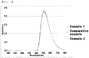
- FIG. 3 is a graph showing the dominant wavelength in Example 1, Example 2 and Comparative Example 1 of the present application. As can be seen in FIG.
- the vehicle lamp according to an embodiment of the present application provides an advantage in terms of the manufacturing process in which the fluorescent film and the color filter comprise the same binder of polydimethylsiloxane (PDMS), and thus the color filter can be directly coated on the fluorescent film without using a solvent and a dispersant.
- PDMS polydimethylsiloxane
- the haze value of the color filter using PDMS is higher than that of the conventional acrylic color filter.
- High haze is advantageous for improving concealment of light-emitting elements in vehicle lamps because light is scattered from the inside. Excessively high haze may cause a decrease in luminance, but only contributes to the improvement of concealment without affecting optical performance, as can be seen from the result of Table 1.
- Example 2 when using the PDMS material as a color filter, as shown in Example 2, although the light-diffusing layer is removed and the thickness of the fluorescent layer is increased, the optical performance and the concealment of the light-emitting element for vehicle lamps are maintained.
- the fluorescent film and the color filter comprise the same binder of polydimethylsiloxane (PDMS), thus enabling the color filter to be directly coated on the fluorescent film without using a solvent and a dispersant, and thus providing an advantage in terms of the manufacturing process compared to the case of using acryl.
- the vehicle lamp according to one embodiment of the present application contains the same material in the light-diffusing layer, the fluorescent film and the color filter, thus advantageously resisting deformation such as warping or twisting and providing excellent optical performance.
Landscapes
- Physics & Mathematics (AREA)
- Engineering & Computer Science (AREA)
- Chemical & Material Sciences (AREA)
- Optics & Photonics (AREA)
- General Physics & Mathematics (AREA)
- Wood Science & Technology (AREA)
- Life Sciences & Earth Sciences (AREA)
- Organic Chemistry (AREA)
- Materials Engineering (AREA)
- General Engineering & Computer Science (AREA)
- Mechanical Engineering (AREA)
- Microelectronics & Electronic Packaging (AREA)
- Chemical Kinetics & Catalysis (AREA)
- Non-Portable Lighting Devices Or Systems Thereof (AREA)
- Optical Elements Other Than Lenses (AREA)
- Optical Filters (AREA)
- Led Device Packages (AREA)
- Planar Illumination Modules (AREA)
Claims (14)
- Fahrzeuglampe mit einer Struktur, bei der ein unteres Substrat, eine fluoreszierende Folie und ein Farbfilter in dieser Reihenfolge übereinander angeordnet sind, wobei die fluoreszierende Folie und der Farbfilter Polydimethylsiloxan (PDMS) umfassen.
- Fahrzeuglampe nach Anspruch 1, weiter umfassend eine Licht zerstreuende Schicht zwischen dem unteren Substrat und der fluoreszierenden Folie.
- Fahrzeuglampe nach Anspruch 2, wobei die Licht zerstreuende Schicht Polydimethylsiloxan (PDMS) umfasst.
- Fahrzeuglampe nach Anspruch 1, wobei das untere Substrat eine Struktur aufweist, bei der ein Substrat, eine erste Elektrode, eine erste isolierende Folie, die ein lichtemittierendes Element umfasst, und eine zweite isolierende Folie, die eine zweite Elektrode umfasst, in dieser Reihenfolge übereinander angeordnet sind,
wobei eine Oberfläche, die gegenüberliegend ist zu einer Oberfläche der zweiten isolierenden Folie in Kontakt mit der ersten isolierenden Folie, und eine Oberfläche, die gegenüberliegend ist zu einer Oberfläche der fluoreszierenden Folie in Kontakt mit dem Farbfilter, miteinander in Kontakt sind. - Fahrzeuglampe nach Anspruch 4, wobei das Substrat ausgewählt ist aus der Gruppe bestehend aus Polyethylenterephthalat (PET), Polyester, Polycarbonat (PC), Polyimid (PI), Polyethylennaphthalat (PEN), Polyetheretherketon (PEEK), Polyarylat (PAR), polycyclischem Olefin (PCO), Polynorbornen, Polyethersulfon (PES) und einem Cycloolefinpolymer (COP).
- Fahrzeuglampe nach Anspruch 1, wobei der Farbfilter eine Dicke von 50 µm oder mehr und 150 µm oder weniger aufweist.
- Fahrzeuglampe nach Anspruch 1, wobei die fluoreszierende Folie eine Dicke von 100 µm oder mehr und 1,000 µm oder weniger aufweist.
- Fahrzeuglampe nach Anspruch 1, wobei der Farbfilter ein Pigment umfasst, wobei das Pigment in einer Menge von 0,5 Gewichtsteilen bis 2 Gewichtsteilen, basierend auf 100 Gewichtsteilen des Polydimethylsiloxans (PDMS), vorhanden ist.
- Fahrzeuglampe nach Anspruch 1, wobei die fluoreszierende Folie ein fluoreszierendes Material umfasst, wobei das fluoreszierende Material in einer Menge von 5 Gewichtsteilen bis 50 Gewichtsteilen, basierend auf 100 Gewichtsteilen des Polydimethylsiloxans (PDMS), vorhanden ist.
- Verfahren zum Herstellen einer Fahrzeuglampe, umfassend:Herstellen eines unteren Substrats;Bilden einer fluoreszierenden Folie auf einer Oberfläche des unteren Substrats; undBilden eines Farbfilters auf einer einer Oberfläche des fluoreszierenden Films in Kontakt mit dem unteren Substrat gegenüberliegenden Oberfläche,wobei die fluoreszierende Folie und der Farbfilter Polydimethylsiloxan (PDMS) umfassen.
- Verfahren nach Anspruch 10, wobei das Herstellen eines unteren Substrats umfasst:Herstellen eines Substrats;Bilden einer ersten Elektrode auf einer Oberfläche des Substrats;Bilden einer ersten isolierenden Folie, die ein lichtemittierendes Element umfasst, auf einer einer ersten Oberfläche der ersten Elektrode in Kontakt mit dem Substrat gegenüberliegenden Oberfläche; undBilden einer zweiten isolierenden Folie, die eine zweite Elektrode umfasst, auf einer einer Oberfläche der ersten isolierenden Folie in Kontakt mit der ersten Elektrode gegenüberliegenden Oberfläche.
- Verfahren nach Anspruch 10, wobei das Bilden eines Farbfilters umfasst:Herstellen einer Farbfilterzusammensetzung, die Polydimethylsiloxan (PDMS) und ein Pigment umfasst; unddirektes Beschichten der Farbfilterzusammensetzung auf einer Oberfläche der fluoreszierenden Folie.
- Verfahren nach Anspruch 12, wobei die Farbfilterzusammensetzung von einem lösungsmittelfreien Typ ist, der kein Lösungsmittel enthält.
- Verfahren nach Anspruch 12, wobei das direkte Beschichten Rakel-Beschichten oder Komma-Beschichten ist.
Applications Claiming Priority (2)
| Application Number | Priority Date | Filing Date | Title |
|---|---|---|---|
| KR1020180132918A KR102334956B1 (ko) | 2018-11-01 | 2018-11-01 | 차량용 램프 및 이의 제조 방법 |
| PCT/KR2019/014565 WO2020091444A1 (ko) | 2018-11-01 | 2019-10-31 | 차량용 램프 및 이의 제조 방법 |
Publications (3)
| Publication Number | Publication Date |
|---|---|
| EP3875845A1 EP3875845A1 (de) | 2021-09-08 |
| EP3875845A4 EP3875845A4 (de) | 2022-02-09 |
| EP3875845B1 true EP3875845B1 (de) | 2022-09-21 |
Family
ID=70462317
Family Applications (1)
| Application Number | Title | Priority Date | Filing Date |
|---|---|---|---|
| EP19877641.1A Active EP3875845B1 (de) | 2018-11-01 | 2019-10-31 | Fahrzeuglampe und verfahren zur herstellung davon |
Country Status (7)
| Country | Link |
|---|---|
| US (1) | US11745641B2 (de) |
| EP (1) | EP3875845B1 (de) |
| JP (1) | JP7130304B2 (de) |
| KR (1) | KR102334956B1 (de) |
| CN (1) | CN112236618B (de) |
| TW (1) | TW202024525A (de) |
| WO (1) | WO2020091444A1 (de) |
Family Cites Families (51)
| Publication number | Priority date | Publication date | Assignee | Title |
|---|---|---|---|---|
| JPH07130471A (ja) * | 1993-11-04 | 1995-05-19 | Nippondenso Co Ltd | エレクトロルミネッセンス素子 |
| JP4271747B2 (ja) * | 1997-07-07 | 2009-06-03 | 株式会社朝日ラバー | 発光ダイオード用透光性被覆材及び蛍光カラー光源 |
| US6319425B1 (en) | 1997-07-07 | 2001-11-20 | Asahi Rubber Inc. | Transparent coating member for light-emitting diodes and a fluorescent color light source |
| GB9801137D0 (en) | 1998-01-20 | 1998-03-18 | Eastman Kodak Co | Time-temparature indicator devices |
| JP4384300B2 (ja) * | 1999-08-31 | 2009-12-16 | ダイセル化学工業株式会社 | タッチパネル及びそれを用いた表示装置 |
| KR20010030164A (ko) * | 1999-08-31 | 2001-04-16 | 고지마 아끼로, 오가와 다이스께 | 터치 패널 및 그것을 이용한 표시 장치 |
| JP4852790B2 (ja) * | 2001-03-22 | 2012-01-11 | 凸版印刷株式会社 | 転写型カラーフィルタの製造方法 |
| US7618709B2 (en) * | 2002-04-30 | 2009-11-17 | Avery Dennison Corporation | Fluorescent articles having multiple film layers |
| US8034173B2 (en) * | 2003-12-18 | 2011-10-11 | Evonik Degussa Gmbh | Processing compositions and method of forming the same |
| KR101119818B1 (ko) | 2004-12-07 | 2012-03-06 | 주식회사 동진쎄미켐 | 컬러필터용 감광성 수지 조성물 및 이를 이용한액정디스플레이 컬러필터의 제조방법 |
| US20060246233A1 (en) * | 2005-04-28 | 2006-11-02 | Fuji Photo Film Co., Ltd. | Light diffusion film, anti-reflection film, polarizing plate and image display device |
| JP4732888B2 (ja) * | 2005-12-19 | 2011-07-27 | 株式会社小糸製作所 | 赤色発光蛍光体およびそれを用いた発光モジュール |
| JP2007266356A (ja) * | 2006-03-29 | 2007-10-11 | Kyocera Corp | 発光装置およびそれを用いた照明装置 |
| KR100783251B1 (ko) * | 2006-04-10 | 2007-12-06 | 삼성전기주식회사 | 양자점을 이용한 다층 구조 백색 발광 다이오드 및 그의제조방법 |
| CN101535177B (zh) * | 2006-11-10 | 2012-06-13 | 住友电气工业株式会社 | 含有Si-O的氢化碳膜、具有该氢化碳膜的光学装置以及制备含有Si-O的氢化碳膜和光学装置的方法 |
| JP5049033B2 (ja) * | 2007-03-08 | 2012-10-17 | 富士フイルム株式会社 | 液晶表示装置 |
| CN101548133B (zh) | 2007-04-12 | 2014-03-12 | 株式会社尼康 | 放电灯、连接用线缆、光源装置及曝光装置 |
| TW200909943A (en) * | 2007-05-21 | 2009-03-01 | Rohm & Haas Denmark Finance As | Thin film bulk and surface diffuser |
| EP2183408A2 (de) * | 2007-08-07 | 2010-05-12 | President And Fellows Of Harvard College | Metalloxidbeschichtung auf oberflächen |
| JP5128888B2 (ja) * | 2007-10-01 | 2013-01-23 | 株式会社朝日ラバー | 発光デバイス及びそれを用いた照明装置 |
| JP5941243B2 (ja) | 2007-10-17 | 2016-06-29 | スタンレー電気株式会社 | 発光装置、それを用いた車両用灯具、およびヘッドランプ |
| KR101608292B1 (ko) | 2008-02-22 | 2016-04-01 | 후지필름 가부시키가이샤 | 착색 경화성 조성물, 착색 패턴, 컬러 필터, 컬러 필터의 제조 방법, 및 액정 표시 소자 |
| JP5047264B2 (ja) | 2009-12-22 | 2012-10-10 | 株式会社東芝 | 発光装置 |
| JP2011208109A (ja) | 2010-03-08 | 2011-10-20 | Asahi Kasei Chemicals Corp | ポリオルガノシロキサンの製造方法 |
| CN101949847B (zh) * | 2010-08-13 | 2012-05-30 | 浙江大学 | 一种无透镜荧光成像检测装置及应用 |
| KR101221470B1 (ko) * | 2011-05-27 | 2013-01-11 | 삼성코닝정밀소재 주식회사 | 액정 디스플레이 장치용 컬러시프트 저감 광학필터 및 이를 구비하는 액정 디스플레이 장치 |
| JP2012247783A (ja) | 2011-05-30 | 2012-12-13 | Samsung Corning Precision Materials Co Ltd | ディスプレイ装置 |
| WO2013035002A2 (en) | 2011-09-09 | 2013-03-14 | Koninklijke Philips Electronics N.V. | Light-emitting arrangement |
| EP2645822A1 (de) * | 2012-03-29 | 2013-10-02 | Koninklijke Philips N.V. | Beleuchtungsvorrichtungen mit mindestens zwei organischen lumineszierenden Materialien |
| KR101427307B1 (ko) | 2012-06-14 | 2014-08-06 | 한국과학기술원 | 금속 나노 입자를 포함하는 컬러 필터 |
| CN102879366B (zh) * | 2012-09-21 | 2015-07-01 | 常州大学 | 检测量子点与生物分子相互作用的液滴微流控系统及方法 |
| KR102171776B1 (ko) * | 2012-10-25 | 2020-10-30 | 루미리즈 홀딩 비.브이. | 실리콘 내의 양자 점을 위한 pdms-기재 리간드 |
| US10035952B2 (en) | 2012-10-25 | 2018-07-31 | Lumileds Llc | PDMS-based ligands for quantum dots in silicones |
| JP5683625B2 (ja) | 2013-03-15 | 2015-03-11 | スタンレー電気株式会社 | 発光装置、それを用いた車両用灯具、およびヘッドランプ |
| EP3064829B1 (de) | 2013-09-13 | 2018-07-25 | Toppan Printing Co., Ltd. | Wellenlängenumwandlungsfolie und hintergrundbeleuchtungseinheit |
| JP6331191B2 (ja) * | 2013-09-20 | 2018-05-30 | 国立大学法人九州大学 | 光測定装置、光測定方法、フィルタ部材及びフィルタ部材を生産する方法 |
| US9835925B1 (en) | 2015-01-08 | 2017-12-05 | E Ink Corporation | Electro-optic displays, and processes for the production thereof |
| KR101614370B1 (ko) | 2015-04-07 | 2016-04-21 | 엘지전자 주식회사 | 반도체 발광소자, 반도체 발광소자의 이송 헤드, 및 반도체 발광소자를 이송하는 방법 |
| CN104793275A (zh) | 2015-04-29 | 2015-07-22 | 宁波江北激智新材料有限公司 | 一种色度坐标和色域范围可调的荧光薄膜 |
| WO2017057454A1 (ja) * | 2015-09-30 | 2017-04-06 | 東レ株式会社 | 発光装置の製造方法および表示装置の製造方法 |
| JP6521177B2 (ja) | 2016-04-25 | 2019-05-29 | 日本製鉄株式会社 | 溶鉄の脱硫方法及び脱硫装置 |
| CN105694042B (zh) * | 2016-04-26 | 2021-04-13 | 京东方科技集团股份有限公司 | 光扩散粉、光扩散粉的制备方法、量子点光刻胶及量子点彩膜 |
| CN105968812B (zh) * | 2016-05-24 | 2019-03-12 | 中国科学院长春光学精密机械与物理研究所 | 聚二甲基硅氧烷的用途、荧光薄膜及其制备方法 |
| KR102513351B1 (ko) * | 2016-06-30 | 2023-03-23 | 엘지전자 주식회사 | 반도체 발광 소자를 이용한 차량용 램프 |
| US10332949B2 (en) | 2016-07-06 | 2019-06-25 | Seoul Semiconductor Co., Ltd. | Display apparatus |
| JP2018049971A (ja) | 2016-09-23 | 2018-03-29 | スタンレー電気株式会社 | 発光装置の製造方法及び発光装置 |
| KR101885656B1 (ko) * | 2016-10-25 | 2018-08-06 | 엘지전자 주식회사 | 차량용 램프 |
| WO2018088387A1 (ja) * | 2016-11-10 | 2018-05-17 | リンテック株式会社 | ガスバリア性積層シート、ガスバリア性積層シートの製造方法、及び電子部材又は光学部材 |
| KR102250527B1 (ko) * | 2016-12-08 | 2021-05-10 | 고려대학교 산학협력단 | 가변 칼라 필터 필름 및 변형률 측정 장치 |
| KR101908218B1 (ko) * | 2016-12-27 | 2018-10-15 | 고려대학교 산학협력단 | Led 조명용 광확산 플레이트 및 이의 제조 방법 |
| CN108388040B (zh) * | 2018-02-08 | 2020-09-22 | 苏州市联超光电科技有限公司 | 一种树脂滤光片及其制备方法 |
-
2018
- 2018-11-01 KR KR1020180132918A patent/KR102334956B1/ko active Active
-
2019
- 2019-10-31 US US15/734,475 patent/US11745641B2/en active Active
- 2019-10-31 JP JP2020568415A patent/JP7130304B2/ja active Active
- 2019-10-31 CN CN201980037558.8A patent/CN112236618B/zh active Active
- 2019-10-31 WO PCT/KR2019/014565 patent/WO2020091444A1/ko not_active Ceased
- 2019-10-31 EP EP19877641.1A patent/EP3875845B1/de active Active
- 2019-10-31 TW TW108139554A patent/TW202024525A/zh unknown
Also Published As
| Publication number | Publication date |
|---|---|
| KR20200050202A (ko) | 2020-05-11 |
| US20210221279A1 (en) | 2021-07-22 |
| US11745641B2 (en) | 2023-09-05 |
| KR102334956B1 (ko) | 2021-12-02 |
| EP3875845A1 (de) | 2021-09-08 |
| WO2020091444A1 (ko) | 2020-05-07 |
| JP2021526241A (ja) | 2021-09-30 |
| CN112236618B (zh) | 2022-07-05 |
| JP7130304B2 (ja) | 2022-09-05 |
| EP3875845A4 (de) | 2022-02-09 |
| TW202024525A (zh) | 2020-07-01 |
| CN112236618A (zh) | 2021-01-15 |
Similar Documents
| Publication | Publication Date | Title |
|---|---|---|
| CN104979455B (zh) | 一种led光源装置及其封装方法及背光模组及显示装置 | |
| CN106015955B (zh) | 照明装置 | |
| JP2007129191A (ja) | 低温同時焼成セラミック(ltcc)テープ組成物、発光ダイオード(led)モジュール、照明デバイス、およびそれらの形成方法 | |
| WO2009116531A1 (ja) | 電子デバイス用基板、有機led素子用積層体及びその製造方法、有機led素子及びその製造方法 | |
| US8710523B2 (en) | Device chip carriers, modules, and methods of forming thereof | |
| CN110467917A (zh) | 量子点材料及其制备方法 | |
| KR20100037577A (ko) | 둘 이상의 입력기를 갖는 무기 후막 ac 전기발광 소자, 및 제조 방법 및 용도 | |
| CN101455123A (zh) | 表面发射型电致发光器件 | |
| US20190387616A1 (en) | Light emitting element | |
| EP3875845B1 (de) | Fahrzeuglampe und verfahren zur herstellung davon | |
| JPH1138918A (ja) | エレクトロルミネッセンス素子およびエレクトロルミネッセンス発光装置 | |
| JP2019503556A (ja) | 蛍光体プレートパッケージ、発光パッケージおよびこれを含む車両用ヘッドランプ | |
| KR20090063032A (ko) | 외장과 방열판 및 인쇄회로를 일체화한 엘이디조명 및 그제조 기술 | |
| JP2014179410A (ja) | 発光部品実装用回路基板及び発光部品実装回路基板 | |
| US20080136314A1 (en) | Highly transmissive electroluminescent lamp | |
| JP2000133465A (ja) | エレクトロルミネッセンス素子およびその製造方法 | |
| KR20160058473A (ko) | 연색성 led 조명기구 | |
| US20100221550A1 (en) | Structure for fluorescent paster | |
| JP2001284053A (ja) | エレクトロルミネッセンス素子 | |
| JP2017033908A (ja) | 有機el素子 | |
| TWI663746B (zh) | 亮度色溫可調光源及其用途 | |
| CN110630913B (zh) | 亮度色温可调光源及其用途 | |
| JP2007134121A (ja) | 発光素子 | |
| JPH02197077A (ja) | Elパネル | |
| CN202145687U (zh) | 无机电致发光元件 |
Legal Events
| Date | Code | Title | Description |
|---|---|---|---|
| STAA | Information on the status of an ep patent application or granted ep patent |
Free format text: STATUS: THE INTERNATIONAL PUBLICATION HAS BEEN MADE |
|
| PUAI | Public reference made under article 153(3) epc to a published international application that has entered the european phase |
Free format text: ORIGINAL CODE: 0009012 |
|
| STAA | Information on the status of an ep patent application or granted ep patent |
Free format text: STATUS: REQUEST FOR EXAMINATION WAS MADE |
|
| 17P | Request for examination filed |
Effective date: 20201130 |
|
| AK | Designated contracting states |
Kind code of ref document: A1 Designated state(s): AL AT BE BG CH CY CZ DE DK EE ES FI FR GB GR HR HU IE IS IT LI LT LU LV MC MK MT NL NO PL PT RO RS SE SI SK SM TR |
|
| A4 | Supplementary search report drawn up and despatched |
Effective date: 20220112 |
|
| DAV | Request for validation of the european patent (deleted) | ||
| DAX | Request for extension of the european patent (deleted) | ||
| RIC1 | Information provided on ipc code assigned before grant |
Ipc: F21Y 115/10 20160101ALI20220104BHEP Ipc: B05D 5/00 20060101ALI20220104BHEP Ipc: B05D 7/24 20060101ALI20220104BHEP Ipc: H05K 1/03 20060101ALI20220104BHEP Ipc: G02B 1/04 20060101ALI20220104BHEP Ipc: G02B 5/20 20060101ALI20220104BHEP Ipc: F21S 41/20 20180101AFI20220104BHEP |
|
| GRAP | Despatch of communication of intention to grant a patent |
Free format text: ORIGINAL CODE: EPIDOSNIGR1 |
|
| STAA | Information on the status of an ep patent application or granted ep patent |
Free format text: STATUS: GRANT OF PATENT IS INTENDED |
|
| RIC1 | Information provided on ipc code assigned before grant |
Ipc: H01L 33/58 20100101ALI20220603BHEP Ipc: H01L 33/50 20100101ALI20220603BHEP Ipc: H01L 33/44 20100101ALI20220603BHEP Ipc: G02B 5/22 20060101ALI20220603BHEP Ipc: C09D 183/04 20060101ALI20220603BHEP Ipc: C08G 77/04 20060101ALI20220603BHEP Ipc: B05D 7/00 20060101ALI20220603BHEP Ipc: B05D 3/02 20060101ALI20220603BHEP Ipc: B05D 1/26 20060101ALI20220603BHEP Ipc: C09D 5/00 20060101ALI20220603BHEP Ipc: F21Y 115/10 20160101ALI20220603BHEP Ipc: B05D 5/00 20060101ALI20220603BHEP Ipc: B05D 7/24 20060101ALI20220603BHEP Ipc: H05K 1/03 20060101ALI20220603BHEP Ipc: G02B 1/04 20060101ALI20220603BHEP Ipc: G02B 5/20 20060101ALI20220603BHEP Ipc: F21S 41/20 20180101AFI20220603BHEP |
|
| INTG | Intention to grant announced |
Effective date: 20220629 |
|
| GRAS | Grant fee paid |
Free format text: ORIGINAL CODE: EPIDOSNIGR3 |
|
| GRAA | (expected) grant |
Free format text: ORIGINAL CODE: 0009210 |
|
| STAA | Information on the status of an ep patent application or granted ep patent |
Free format text: STATUS: THE PATENT HAS BEEN GRANTED |
|
| AK | Designated contracting states |
Kind code of ref document: B1 Designated state(s): AL AT BE BG CH CY CZ DE DK EE ES FI FR GB GR HR HU IE IS IT LI LT LU LV MC MK MT NL NO PL PT RO RS SE SI SK SM TR |
|
| REG | Reference to a national code |
Ref country code: GB Ref legal event code: FG4D |
|
| REG | Reference to a national code |
Ref country code: CH Ref legal event code: EP |
|
| REG | Reference to a national code |
Ref country code: DE Ref legal event code: R096 Ref document number: 602019019903 Country of ref document: DE |
|
| REG | Reference to a national code |
Ref country code: IE Ref legal event code: FG4D |
|
| REG | Reference to a national code |
Ref country code: AT Ref legal event code: REF Ref document number: 1520108 Country of ref document: AT Kind code of ref document: T Effective date: 20221015 |
|
| REG | Reference to a national code |
Ref country code: LT Ref legal event code: MG9D |
|
| REG | Reference to a national code |
Ref country code: NL Ref legal event code: MP Effective date: 20220921 |
|
| PG25 | Lapsed in a contracting state [announced via postgrant information from national office to epo] |
Ref country code: SE Free format text: LAPSE BECAUSE OF FAILURE TO SUBMIT A TRANSLATION OF THE DESCRIPTION OR TO PAY THE FEE WITHIN THE PRESCRIBED TIME-LIMIT Effective date: 20220921 Ref country code: RS Free format text: LAPSE BECAUSE OF FAILURE TO SUBMIT A TRANSLATION OF THE DESCRIPTION OR TO PAY THE FEE WITHIN THE PRESCRIBED TIME-LIMIT Effective date: 20220921 Ref country code: NO Free format text: LAPSE BECAUSE OF FAILURE TO SUBMIT A TRANSLATION OF THE DESCRIPTION OR TO PAY THE FEE WITHIN THE PRESCRIBED TIME-LIMIT Effective date: 20221221 Ref country code: LV Free format text: LAPSE BECAUSE OF FAILURE TO SUBMIT A TRANSLATION OF THE DESCRIPTION OR TO PAY THE FEE WITHIN THE PRESCRIBED TIME-LIMIT Effective date: 20220921 Ref country code: LT Free format text: LAPSE BECAUSE OF FAILURE TO SUBMIT A TRANSLATION OF THE DESCRIPTION OR TO PAY THE FEE WITHIN THE PRESCRIBED TIME-LIMIT Effective date: 20220921 Ref country code: FI Free format text: LAPSE BECAUSE OF FAILURE TO SUBMIT A TRANSLATION OF THE DESCRIPTION OR TO PAY THE FEE WITHIN THE PRESCRIBED TIME-LIMIT Effective date: 20220921 |
|
| REG | Reference to a national code |
Ref country code: AT Ref legal event code: MK05 Ref document number: 1520108 Country of ref document: AT Kind code of ref document: T Effective date: 20220921 |
|
| PG25 | Lapsed in a contracting state [announced via postgrant information from national office to epo] |
Ref country code: HR Free format text: LAPSE BECAUSE OF FAILURE TO SUBMIT A TRANSLATION OF THE DESCRIPTION OR TO PAY THE FEE WITHIN THE PRESCRIBED TIME-LIMIT Effective date: 20220921 Ref country code: GR Free format text: LAPSE BECAUSE OF FAILURE TO SUBMIT A TRANSLATION OF THE DESCRIPTION OR TO PAY THE FEE WITHIN THE PRESCRIBED TIME-LIMIT Effective date: 20221222 |
|
| PG25 | Lapsed in a contracting state [announced via postgrant information from national office to epo] |
Ref country code: SM Free format text: LAPSE BECAUSE OF FAILURE TO SUBMIT A TRANSLATION OF THE DESCRIPTION OR TO PAY THE FEE WITHIN THE PRESCRIBED TIME-LIMIT Effective date: 20220921 Ref country code: RO Free format text: LAPSE BECAUSE OF FAILURE TO SUBMIT A TRANSLATION OF THE DESCRIPTION OR TO PAY THE FEE WITHIN THE PRESCRIBED TIME-LIMIT Effective date: 20220921 Ref country code: PT Free format text: LAPSE BECAUSE OF FAILURE TO SUBMIT A TRANSLATION OF THE DESCRIPTION OR TO PAY THE FEE WITHIN THE PRESCRIBED TIME-LIMIT Effective date: 20230123 Ref country code: ES Free format text: LAPSE BECAUSE OF FAILURE TO SUBMIT A TRANSLATION OF THE DESCRIPTION OR TO PAY THE FEE WITHIN THE PRESCRIBED TIME-LIMIT Effective date: 20220921 Ref country code: CZ Free format text: LAPSE BECAUSE OF FAILURE TO SUBMIT A TRANSLATION OF THE DESCRIPTION OR TO PAY THE FEE WITHIN THE PRESCRIBED TIME-LIMIT Effective date: 20220921 Ref country code: AT Free format text: LAPSE BECAUSE OF FAILURE TO SUBMIT A TRANSLATION OF THE DESCRIPTION OR TO PAY THE FEE WITHIN THE PRESCRIBED TIME-LIMIT Effective date: 20220921 |
|
| PG25 | Lapsed in a contracting state [announced via postgrant information from national office to epo] |
Ref country code: SK Free format text: LAPSE BECAUSE OF FAILURE TO SUBMIT A TRANSLATION OF THE DESCRIPTION OR TO PAY THE FEE WITHIN THE PRESCRIBED TIME-LIMIT Effective date: 20220921 Ref country code: PL Free format text: LAPSE BECAUSE OF FAILURE TO SUBMIT A TRANSLATION OF THE DESCRIPTION OR TO PAY THE FEE WITHIN THE PRESCRIBED TIME-LIMIT Effective date: 20220921 Ref country code: IS Free format text: LAPSE BECAUSE OF FAILURE TO SUBMIT A TRANSLATION OF THE DESCRIPTION OR TO PAY THE FEE WITHIN THE PRESCRIBED TIME-LIMIT Effective date: 20230121 Ref country code: EE Free format text: LAPSE BECAUSE OF FAILURE TO SUBMIT A TRANSLATION OF THE DESCRIPTION OR TO PAY THE FEE WITHIN THE PRESCRIBED TIME-LIMIT Effective date: 20220921 |
|
| REG | Reference to a national code |
Ref country code: CH Ref legal event code: PL |
|
| REG | Reference to a national code |
Ref country code: DE Ref legal event code: R097 Ref document number: 602019019903 Country of ref document: DE |
|
| REG | Reference to a national code |
Ref country code: BE Ref legal event code: MM Effective date: 20221031 |
|
| PG25 | Lapsed in a contracting state [announced via postgrant information from national office to epo] |
Ref country code: NL Free format text: LAPSE BECAUSE OF FAILURE TO SUBMIT A TRANSLATION OF THE DESCRIPTION OR TO PAY THE FEE WITHIN THE PRESCRIBED TIME-LIMIT Effective date: 20220921 Ref country code: MC Free format text: LAPSE BECAUSE OF FAILURE TO SUBMIT A TRANSLATION OF THE DESCRIPTION OR TO PAY THE FEE WITHIN THE PRESCRIBED TIME-LIMIT Effective date: 20220921 Ref country code: LU Free format text: LAPSE BECAUSE OF NON-PAYMENT OF DUE FEES Effective date: 20221031 Ref country code: AL Free format text: LAPSE BECAUSE OF FAILURE TO SUBMIT A TRANSLATION OF THE DESCRIPTION OR TO PAY THE FEE WITHIN THE PRESCRIBED TIME-LIMIT Effective date: 20220921 |
|
| PLBE | No opposition filed within time limit |
Free format text: ORIGINAL CODE: 0009261 |
|
| STAA | Information on the status of an ep patent application or granted ep patent |
Free format text: STATUS: NO OPPOSITION FILED WITHIN TIME LIMIT |
|
| PG25 | Lapsed in a contracting state [announced via postgrant information from national office to epo] |
Ref country code: LI Free format text: LAPSE BECAUSE OF NON-PAYMENT OF DUE FEES Effective date: 20221031 Ref country code: DK Free format text: LAPSE BECAUSE OF FAILURE TO SUBMIT A TRANSLATION OF THE DESCRIPTION OR TO PAY THE FEE WITHIN THE PRESCRIBED TIME-LIMIT Effective date: 20220921 Ref country code: CH Free format text: LAPSE BECAUSE OF NON-PAYMENT OF DUE FEES Effective date: 20221031 |
|
| 26N | No opposition filed |
Effective date: 20230622 |
|
| PG25 | Lapsed in a contracting state [announced via postgrant information from national office to epo] |
Ref country code: SI Free format text: LAPSE BECAUSE OF FAILURE TO SUBMIT A TRANSLATION OF THE DESCRIPTION OR TO PAY THE FEE WITHIN THE PRESCRIBED TIME-LIMIT Effective date: 20220921 |
|
| PG25 | Lapsed in a contracting state [announced via postgrant information from national office to epo] |
Ref country code: BE Free format text: LAPSE BECAUSE OF NON-PAYMENT OF DUE FEES Effective date: 20221031 |
|
| PG25 | Lapsed in a contracting state [announced via postgrant information from national office to epo] |
Ref country code: IE Free format text: LAPSE BECAUSE OF NON-PAYMENT OF DUE FEES Effective date: 20221031 |
|
| PG25 | Lapsed in a contracting state [announced via postgrant information from national office to epo] |
Ref country code: CY Free format text: LAPSE BECAUSE OF FAILURE TO SUBMIT A TRANSLATION OF THE DESCRIPTION OR TO PAY THE FEE WITHIN THE PRESCRIBED TIME-LIMIT Effective date: 20220921 |
|
| PG25 | Lapsed in a contracting state [announced via postgrant information from national office to epo] |
Ref country code: MK Free format text: LAPSE BECAUSE OF FAILURE TO SUBMIT A TRANSLATION OF THE DESCRIPTION OR TO PAY THE FEE WITHIN THE PRESCRIBED TIME-LIMIT Effective date: 20220921 Ref country code: IT Free format text: LAPSE BECAUSE OF FAILURE TO SUBMIT A TRANSLATION OF THE DESCRIPTION OR TO PAY THE FEE WITHIN THE PRESCRIBED TIME-LIMIT Effective date: 20220921 Ref country code: HU Free format text: LAPSE BECAUSE OF FAILURE TO SUBMIT A TRANSLATION OF THE DESCRIPTION OR TO PAY THE FEE WITHIN THE PRESCRIBED TIME-LIMIT; INVALID AB INITIO Effective date: 20191031 |
|
| PG25 | Lapsed in a contracting state [announced via postgrant information from national office to epo] |
Ref country code: TR Free format text: LAPSE BECAUSE OF FAILURE TO SUBMIT A TRANSLATION OF THE DESCRIPTION OR TO PAY THE FEE WITHIN THE PRESCRIBED TIME-LIMIT Effective date: 20220921 |
|
| PG25 | Lapsed in a contracting state [announced via postgrant information from national office to epo] |
Ref country code: BG Free format text: LAPSE BECAUSE OF FAILURE TO SUBMIT A TRANSLATION OF THE DESCRIPTION OR TO PAY THE FEE WITHIN THE PRESCRIBED TIME-LIMIT Effective date: 20220921 |
|
| PG25 | Lapsed in a contracting state [announced via postgrant information from national office to epo] |
Ref country code: MT Free format text: LAPSE BECAUSE OF FAILURE TO SUBMIT A TRANSLATION OF THE DESCRIPTION OR TO PAY THE FEE WITHIN THE PRESCRIBED TIME-LIMIT Effective date: 20220921 |
|
| PGFP | Annual fee paid to national office [announced via postgrant information from national office to epo] |
Ref country code: GB Payment date: 20250922 Year of fee payment: 7 |
|
| PGFP | Annual fee paid to national office [announced via postgrant information from national office to epo] |
Ref country code: FR Payment date: 20250925 Year of fee payment: 7 |
|
| PGFP | Annual fee paid to national office [announced via postgrant information from national office to epo] |
Ref country code: DE Payment date: 20250922 Year of fee payment: 7 |