EP3866262B1 - Rfid-etikett - Google Patents
Rfid-etikett Download PDFInfo
- Publication number
- EP3866262B1 EP3866262B1 EP21167029.4A EP21167029A EP3866262B1 EP 3866262 B1 EP3866262 B1 EP 3866262B1 EP 21167029 A EP21167029 A EP 21167029A EP 3866262 B1 EP3866262 B1 EP 3866262B1
- Authority
- EP
- European Patent Office
- Prior art keywords
- antenna
- chip
- rfid tag
- turns
- conductor
- Prior art date
- Legal status (The legal status is an assumption and is not a legal conclusion. Google has not performed a legal analysis and makes no representation as to the accuracy of the status listed.)
- Active
Links
Images


Classifications
-
- G—PHYSICS
- G06—COMPUTING OR CALCULATING; COUNTING
- G06K—GRAPHICAL DATA READING; PRESENTATION OF DATA; RECORD CARRIERS; HANDLING RECORD CARRIERS
- G06K19/00—Record carriers for use with machines and with at least a part designed to carry digital markings
- G06K19/06—Record carriers for use with machines and with at least a part designed to carry digital markings characterised by the kind of the digital marking, e.g. shape, nature, code
- G06K19/067—Record carriers with conductive marks, printed circuits or semiconductor circuit elements, e.g. credit or identity cards also with resonating or responding marks without active components
- G06K19/07—Record carriers with conductive marks, printed circuits or semiconductor circuit elements, e.g. credit or identity cards also with resonating or responding marks without active components with integrated circuit chips
- G06K19/077—Constructional details, e.g. mounting of circuits in the carrier
- G06K19/07749—Constructional details, e.g. mounting of circuits in the carrier the record carrier being capable of non-contact communication, e.g. constructional details of the antenna of a non-contact smart card
- G06K19/07773—Antenna details
- G06K19/07777—Antenna details the antenna being of the inductive type
- G06K19/07779—Antenna details the antenna being of the inductive type the inductive antenna being a coil
- G06K19/07783—Antenna details the antenna being of the inductive type the inductive antenna being a coil the coil being planar
-
- G—PHYSICS
- G06—COMPUTING OR CALCULATING; COUNTING
- G06K—GRAPHICAL DATA READING; PRESENTATION OF DATA; RECORD CARRIERS; HANDLING RECORD CARRIERS
- G06K19/00—Record carriers for use with machines and with at least a part designed to carry digital markings
- G06K19/06—Record carriers for use with machines and with at least a part designed to carry digital markings characterised by the kind of the digital marking, e.g. shape, nature, code
- G06K19/067—Record carriers with conductive marks, printed circuits or semiconductor circuit elements, e.g. credit or identity cards also with resonating or responding marks without active components
- G06K19/07—Record carriers with conductive marks, printed circuits or semiconductor circuit elements, e.g. credit or identity cards also with resonating or responding marks without active components with integrated circuit chips
- G06K19/0723—Record carriers with conductive marks, printed circuits or semiconductor circuit elements, e.g. credit or identity cards also with resonating or responding marks without active components with integrated circuit chips the record carrier comprising an arrangement for non-contact communication, e.g. wireless communication circuits on transponder cards, non-contact smart cards or RFIDs
- G06K19/0724—Record carriers with conductive marks, printed circuits or semiconductor circuit elements, e.g. credit or identity cards also with resonating or responding marks without active components with integrated circuit chips the record carrier comprising an arrangement for non-contact communication, e.g. wireless communication circuits on transponder cards, non-contact smart cards or RFIDs the arrangement being a circuit for communicating at a plurality of frequencies, e.g. for managing time multiplexed communication over at least two antennas of different types
-
- G—PHYSICS
- G06—COMPUTING OR CALCULATING; COUNTING
- G06K—GRAPHICAL DATA READING; PRESENTATION OF DATA; RECORD CARRIERS; HANDLING RECORD CARRIERS
- G06K19/00—Record carriers for use with machines and with at least a part designed to carry digital markings
- G06K19/06—Record carriers for use with machines and with at least a part designed to carry digital markings characterised by the kind of the digital marking, e.g. shape, nature, code
- G06K19/067—Record carriers with conductive marks, printed circuits or semiconductor circuit elements, e.g. credit or identity cards also with resonating or responding marks without active components
- G06K19/07—Record carriers with conductive marks, printed circuits or semiconductor circuit elements, e.g. credit or identity cards also with resonating or responding marks without active components with integrated circuit chips
- G06K19/077—Constructional details, e.g. mounting of circuits in the carrier
- G06K19/07749—Constructional details, e.g. mounting of circuits in the carrier the record carrier being capable of non-contact communication, e.g. constructional details of the antenna of a non-contact smart card
- G06K19/0775—Constructional details, e.g. mounting of circuits in the carrier the record carrier being capable of non-contact communication, e.g. constructional details of the antenna of a non-contact smart card arrangements for connecting the integrated circuit to the antenna
- G06K19/07754—Constructional details, e.g. mounting of circuits in the carrier the record carrier being capable of non-contact communication, e.g. constructional details of the antenna of a non-contact smart card arrangements for connecting the integrated circuit to the antenna the connection being galvanic
-
- G—PHYSICS
- G06—COMPUTING OR CALCULATING; COUNTING
- G06K—GRAPHICAL DATA READING; PRESENTATION OF DATA; RECORD CARRIERS; HANDLING RECORD CARRIERS
- G06K19/00—Record carriers for use with machines and with at least a part designed to carry digital markings
- G06K19/06—Record carriers for use with machines and with at least a part designed to carry digital markings characterised by the kind of the digital marking, e.g. shape, nature, code
- G06K19/067—Record carriers with conductive marks, printed circuits or semiconductor circuit elements, e.g. credit or identity cards also with resonating or responding marks without active components
- G06K19/07—Record carriers with conductive marks, printed circuits or semiconductor circuit elements, e.g. credit or identity cards also with resonating or responding marks without active components with integrated circuit chips
- G06K19/077—Constructional details, e.g. mounting of circuits in the carrier
- G06K19/07749—Constructional details, e.g. mounting of circuits in the carrier the record carrier being capable of non-contact communication, e.g. constructional details of the antenna of a non-contact smart card
- G06K19/07773—Antenna details
- G06K19/07775—Antenna details the antenna being on-chip
-
- G—PHYSICS
- G06—COMPUTING OR CALCULATING; COUNTING
- G06K—GRAPHICAL DATA READING; PRESENTATION OF DATA; RECORD CARRIERS; HANDLING RECORD CARRIERS
- G06K19/00—Record carriers for use with machines and with at least a part designed to carry digital markings
- G06K19/06—Record carriers for use with machines and with at least a part designed to carry digital markings characterised by the kind of the digital marking, e.g. shape, nature, code
- G06K19/067—Record carriers with conductive marks, printed circuits or semiconductor circuit elements, e.g. credit or identity cards also with resonating or responding marks without active components
- G06K19/07—Record carriers with conductive marks, printed circuits or semiconductor circuit elements, e.g. credit or identity cards also with resonating or responding marks without active components with integrated circuit chips
- G06K19/077—Constructional details, e.g. mounting of circuits in the carrier
- G06K19/07749—Constructional details, e.g. mounting of circuits in the carrier the record carrier being capable of non-contact communication, e.g. constructional details of the antenna of a non-contact smart card
- G06K19/07773—Antenna details
- G06K19/07786—Antenna details the antenna being of the HF type, such as a dipole
-
- G—PHYSICS
- G06—COMPUTING OR CALCULATING; COUNTING
- G06K—GRAPHICAL DATA READING; PRESENTATION OF DATA; RECORD CARRIERS; HANDLING RECORD CARRIERS
- G06K19/00—Record carriers for use with machines and with at least a part designed to carry digital markings
- G06K19/06—Record carriers for use with machines and with at least a part designed to carry digital markings characterised by the kind of the digital marking, e.g. shape, nature, code
- G06K19/067—Record carriers with conductive marks, printed circuits or semiconductor circuit elements, e.g. credit or identity cards also with resonating or responding marks without active components
- G06K19/07—Record carriers with conductive marks, printed circuits or semiconductor circuit elements, e.g. credit or identity cards also with resonating or responding marks without active components with integrated circuit chips
- G06K19/077—Constructional details, e.g. mounting of circuits in the carrier
- G06K19/07749—Constructional details, e.g. mounting of circuits in the carrier the record carrier being capable of non-contact communication, e.g. constructional details of the antenna of a non-contact smart card
- G06K19/07773—Antenna details
- G06K19/07794—Antenna details the record carrier comprising a booster or auxiliary antenna in addition to the antenna connected directly to the integrated circuit
-
- H—ELECTRICITY
- H01—ELECTRIC ELEMENTS
- H01Q—ANTENNAS, i.e. RADIO AERIALS
- H01Q1/00—Details of, or arrangements associated with, antennas
- H01Q1/12—Supports; Mounting means
- H01Q1/22—Supports; Mounting means by structural association with other equipment or articles
- H01Q1/2208—Supports; Mounting means by structural association with other equipment or articles associated with components used in interrogation type services, i.e. in systems for information exchange between an interrogator/reader and a tag/transponder, e.g. in Radio Frequency Identification [RFID] systems
- H01Q1/2225—Supports; Mounting means by structural association with other equipment or articles associated with components used in interrogation type services, i.e. in systems for information exchange between an interrogator/reader and a tag/transponder, e.g. in Radio Frequency Identification [RFID] systems used in active tags, i.e. provided with its own power source or in passive tags, i.e. deriving power from RF signal
-
- H—ELECTRICITY
- H01—ELECTRIC ELEMENTS
- H01Q—ANTENNAS, i.e. RADIO AERIALS
- H01Q7/00—Loop antennas with a substantially uniform current distribution around the loop and having a directional radiation pattern in a plane perpendicular to the plane of the loop
-
- H—ELECTRICITY
- H04—ELECTRIC COMMUNICATION TECHNIQUE
- H04B—TRANSMISSION
- H04B5/00—Near-field transmission systems, e.g. inductive or capacitive transmission systems
- H04B5/20—Near-field transmission systems, e.g. inductive or capacitive transmission systems characterised by the transmission technique; characterised by the transmission medium
- H04B5/24—Inductive coupling
- H04B5/26—Inductive coupling using coils
-
- H—ELECTRICITY
- H04—ELECTRIC COMMUNICATION TECHNIQUE
- H04B—TRANSMISSION
- H04B5/00—Near-field transmission systems, e.g. inductive or capacitive transmission systems
- H04B5/40—Near-field transmission systems, e.g. inductive or capacitive transmission systems characterised by components specially adapted for near-field transmission
- H04B5/48—Transceivers
-
- H—ELECTRICITY
- H04—ELECTRIC COMMUNICATION TECHNIQUE
- H04B—TRANSMISSION
- H04B5/00—Near-field transmission systems, e.g. inductive or capacitive transmission systems
- H04B5/70—Near-field transmission systems, e.g. inductive or capacitive transmission systems specially adapted for specific purposes
- H04B5/77—Near-field transmission systems, e.g. inductive or capacitive transmission systems specially adapted for specific purposes for interrogation
Definitions
- the present invention relates to a booster antenna for a spiral-shaped antenna of a tag for performing non-contact transmission/reception of signals with a reader/writer.
- An RFID tag includes an IC chip configured to record information and an antenna connected to the IC chip.
- wireless communication with the reader/writer is performed by the antenna, and thereby information stored in the IC chip is read out, or information is written in the IC chip.
- the antenna of the RFID tag is constituted by a multilayer antenna stacked over the IC chip and integrally joined thereto.
- the multilayer antenna includes a base material having substantially the same outer dimensions as the IC chip, a first coil formed on the base material, a second coil stacked on the first coil via an insulation film, and a protective film protecting the second coil.
- the antenna is a multilayer antenna, and therefore has a large number of turns.
- the RFID tag is said to be capable of improving antenna efficiency (such as the communication distance).
- antenna efficiency such as the communication distance
- Patent Literature 1 JP 4713621 B2
- JP 2009 027741 A relates to an antenna-mounted communication IC unit suitably used for a small portable communication terminal, a non-contact IC card, and the like.
- US 2014/184462 A1 relates to an antenna module and radio communication device.
- US 2014/062827 A1 relates to a RFID which includes an antenna element and a feed device.
- US 2015/087243 A1 relates to a semi-conductor device.
- the present invention has been devised in view of such circumstances, and an object thereof is to provide a booster antenna capable of improving antenna efficiency with a simple configuration.
- the present invention relates to a booster antenna according to claim 1 or 2.
- Fig. 1A shows a passive RFID tag 4 in which an antenna 3 is electrically conductively mounted along the outer peripheral edges on the upper surface of a package (an insulating layer made of resin) of an IC chip 1 via an insulating layer 2.
- the IC chip 1 has a substantially square shape in plan view.
- the IC chip 1 may also have a shape such as a circular, elliptical, or polygonal shape.
- the IC chip 1 of 0.5 mm square (length 0.5 mm ⁇ width 0.5 mm) to 0.9 mm square (length 0.9 mm ⁇ width 0.9 mm) can be used, and the IC chip 1 of 0.9 mm square (length 0.9 mm ⁇ width 0.9 mm) is used in this embodiment.
- the IC chip 1 includes connection terminals 5A, 5B, 5C, and 5D provided inside the outer peripheral edges at the four corners.
- connection terminals 5A and 5B disposed on the upper side of the page in Fig. 1A are connected to the antenna. More specifically, one end of the antenna 3 is connected to the input and output terminal 5A on one side (on the upper left side of the page in Fig. 1A ), and the other end of the antenna 3 is connected to the input and output terminal 5B on the other side (on the upper right side of the page in Fig. 1A ).
- the two connection terminals 5C and 5D disposed on the lower side of the page in Fig. 1A are dummy terminals.
- the connection terminal 5A to which the one end of the antenna 3 is connected and the connection terminal 5B to which the other end of the antenna 3 is connected may be referred to as the input and output terminals 5A and 5B, respectively.
- the insulating layer 2 is made of polyimide, epoxy resin, silicone resin, or the like, and is formed by spin coating, printing, or lamination. Further, the insulating layer 2 can be formed also by attaching a sheet or a film formed of a photosensitive resin such as photosensitive polyimide.
- An annular antenna-forming area is set along substantially the entire outer periphery of the package of the IC chip 1.
- the reason why such an area is set along substantially the entire outer periphery of the package is that a conductor line 3a connected to the connection terminal 5B is wound inside the connection terminal 5B, not between the connection terminal 5B and the outer peripheral edges of the package, so that the conductor line 3a does not overlap itself that is wound inwardly.
- the antenna-forming area is set to have a specific width in a direction orthogonal to its circumferential direction.
- the antenna 3 has a spiral-shaped conductor pattern formed within the antenna-forming area (inside the outer peripheral edges on the upper surface of the package (installation surface)).
- the conductor pattern is in a shape that is wound multiple times (4.75 times in Fig. 1A ) to be almost rectangular, and the portion where the winding of the conductor pattern starts extends straight from the connection terminal 5B toward an outer peripheral edge of the package and has a shape bending before the outer peripheral edge of the package.
- each round starting from the winding start of the conductor pattern may be referred to as a turn in the description.
- the innermost portion of the conductor pattern has a length less than one round but will be referred to as a turn in the same manner as the first round to the fourth round.
- the conductor pattern various conductive materials can be used, where copper, silver, aluminum, and the like can be used, for example. Further, the conductor pattern is formed by various fabrication methods such as a thick-film method in which a conductor paste is applied and baked, sputtering, vapor deposition, vacuum plating, photolithography, and printing.
- Each turn of the conductor pattern includes a plurality of sides of the conductor line 3a disposed corresponding to the outer peripheral edges of the upper surface of the package (installation surface).
- the plurality of sides of conductor line 3a are continuous with each other and are formed into a spiral so as to be turned within the antenna-forming area, with the input and output terminal 5A on one side serving as a starting point and the input and output terminal 5B on the other side serving as an endpoint.
- the aspect ratio of the conductor line 3a is set within the range of 1.0 to 5.0.
- the larger the aspect ratio the larger the cross-sectional area of the conductor line 3a becomes, thereby reducing resistance components of the wiring of the antenna 3, which is preferable for the antenna 3.
- the limit value of the aspect ratio in the antenna 3 is 5.0.
- the minimum value of the aspect ratio is 1.0.
- the aspect ratio is a ratio (H/L) of a long-side length (longitudinal dimension) H with respect to a short-side length (lateral dimension) L in the longitudinal section of the conductor line 3a.
- the normal direction to the installation surface of the antenna 3 may be referred to as the longitudinal direction
- the plane direction of the installation surface of the antenna 3 may be referred to as the lateral direction.
- the opening area of an opening 3K of the conductor pattern is an area surrounded by the four sides of the conductor line 3a located on the innermost edges in the radial direction of the conductor line 3a, that is, surrounded by the conductor line 3a included in the fifth turn from the outside of the conductor pattern (which will be hereinafter referred to as first conductor line 3A) (see Fig. 1A ).
- the line width of the conductor line 3a that is, the lateral dimension L of the conductor line 3a (see Fig. 2A ) is constant or substantially constant across the full length of the conductor line 3a.
- the line width L of the conductor line 3a can be set to any value within the range of 2 pm to 7 pm and is set to 2 pm in this embodiment.
- a spacing (so-called line spacing) S between the turns of the conductor line that are adjacent to each other in the radial direction can be set to any value within the range of 2 pm to 7 pm.
- the conductor pattern is formed by the conductor line 3a wound into a spiral shape inside the outer peripheral edges on the upper surface of the IC chip 1.
- the conductor line 3a is wound into a spiral with its position shifted inwardly in every round. Therefore, the conductor line 3a is wound into a spiral at the spacing S from the portion of the conductor line 3a already provided on the upper surface of the IC chip 1. In the conductor line 3a, the spacing S has a constant distance at each position in the winding direction.
- the winding start portion of the conductor pattern extends from the input and output terminal 5B toward an outer peripheral edge of the package so that the conductor line 3a does not come into contact with itself that is thus connected to the input and output terminal 5B, and the portion following the winding start portion passes inside the input and output terminal 5B.
- the IC chip 1 is 0.9 mm square (length 0.9 mm ⁇ width 0.9 mm), and distances Z1 and Z2 from the outermost edges of the IC chip 1 to the input and output terminal 5A (the input and output terminal on the upper left side in Fig. 1B ) are 65 ⁇ m and 65 ⁇ m, respectively.
- the conductor line 3a in the first turn (one round from the winding start) to the fourth turn of the conductor pattern is disposed so as to pass between the input and output terminal 5A and the outermost edges of the IC chip 1.
- the conductor line 3a in the first to fourth turns of the conductor pattern passes also between the two dummy terminals 5C and 5D and the outermost edges of the IC chip 1.
- the conductor line 3a in the first to fourth turns of the conductor pattern is wound into a spiral and sequentially passes outside the connection terminals 5D, 5C, and 5A (between the connection terminals 5D, 5C, and 5A and the outer peripheral edges of the package) and inside the connection terminal 5B, which thereby allows the conductor line 3a to be wound into a spiral so as not to overlap itself in the inward and outward directions.
- the conductor line 3a included in the fifth turn of the conductor pattern passes inside the dummy terminals 5C and 5D.
- the number of turns in the antenna is 4.75 but is set to any number from 1.5 to 10 corresponding to the resonance frequency (which is herein 920 MHz).
- the line width L of the conductor line 3a is set to a value within the range of 2 pm to 7 ⁇ m.
- the distance is set to a value within the range of 2 ⁇ m to ⁇ pm.
- the distances Z1 and Z2 from the outermost edges of the IC chip 1 to the input and output terminal 5A are not limited to 65 ⁇ m and 65 ⁇ m, respectively, and can be set to any numerical values within the range of 30 ⁇ m to 90 ⁇ m, respectively. Further, although the case where the distance Z1 and the distance Z2 from the outermost edges of the IC chip 1 to the input and output terminal 5A are the same as each other is described herein, the distance Z1 and the distance Z2 may be different from each other.
- the resonance frequency of the RFID tag configured as above is set to 920 MHz.
- L represents the equivalent inductance
- C represents the equivalent capacity of the IC chip generated between the input and output terminals 5A and 5B.
- C is a unique value determined for each IC chip 1, and therefore it is necessary to appropriately set the value L based on the value C, and the value L is determined corresponding to the aspect ratio of the conductor line 3a, the line width L, and the spacing S between the turns of the conductor line 3a. These values are set within the aforementioned ranges.
- the values of the aspect ratio of the conductor line 3a, the line width L, the spacing S between the turns of the conductor line 3a are set in the aforementioned ranges so that the conductor pattern 3 in which the conductor line 3A or 3a disposed close to the outer peripheral edges of the insulating layer is formed.
- the radius of the antenna can be increased while the resistance to the current flowing through the conductor line is suppressed, and thus antenna efficiency (communication distance) can be improved by increasing the antenna gain (gain).
- the upper surface of the IC chip 1 is coated with PI (polyimide) as an insulating layer. Then, the insulating layer is further coated with a seed layer for plating by sputtering. Further, a mold for depositing an antenna pattern is formed over the seed layer using a photoresist.
- PI polyimide
- the process proceeds to a plating step, and the antenna pattern is deposited. Thereafter, the mold layer is removed, and then the exposed unnecessary seed layer is removed. Thereafter, a protective film to protect the antenna pattern is coated with PI (polyimide)to finish the production of the RFID tag.
- PI polyimide
- the RFID tag 4 includes the aforementioned antenna 3 provided on the upper surface of the IC chip 1 and a booster antenna 6 according to the claimed invention configured to operate at substantially the same frequency.
- the RFID tag 4 according to this embodiment has an advantage of being capable of enhancing the transmission/reception sensitivity and thereby increasing the information transmission distance, by including the booster antenna 6.
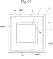
- the antenna 3 mounted on the IC chip 1 has the same configuration as in Fig. 1A , Fig. 1B , Fig. 2A , and Fig. 2B , and therefore the relevant descriptions are omitted. In Fig. 3B and Fig. 3C , the antenna 3 is not shown.
- the booster antenna 6 includes a conductor pattern (antenna) 9 in which a conductor line 9a is wound substantially 1.75 times (which may be multiple turns of 2 times or more up to 5 times) spirally in a ceramic insulating layer 8 stacked on the outer periphery of a ceramic rectangular base 7 (which may be made of other various synthetic resin materials) as an insulating layer (installation plane).
- a ceramic mount 10 having a recess 10A that is rectangular in plan view and is configured to mount the IC chip 1 is formed on the insulating layer 8.
- the antenna 9 is configured to resonate at the same frequency as that of the IC chip 1.
- the antenna 9 performs communication by being electromagnetically coupled to the antenna 3 of the IC chip 1. That is, the IC chip 1 performs communication with a reader/writer via the booster antenna 6. Accordingly, although the size of the antenna 3 of the IC chip 1 is small, the communication distance can be increased by performing communication via the booster antenna 6 that is larger than the antenna 3 of the IC chip 1.
- the reader/writer is a device capable of communicating with the IC chip 1.
- the antenna 3 of the IC chip 1 is constituted by an on-chip antenna in which the antenna 3 is integrally formed with the IC chip 1 itself, the need for contact points to connect the IC chip 1 and the antenna 3 to each other is eliminated.
- the IC chip 1 and the booster antenna 6 are electromagnetically coupled to each other, there is an advantage of being environmentally resistant.
- the line may be disconnected in connected portions between the antenna and the IC (including adhesives), narrow-pattern portions of the antenna, or other portions due to vibration or deformation resulting from differences in thermal expansion among the antenna material, the base material, the adhesives, or the like.
- the IC chip 1 needs only to be installed around the center of the booster antenna 6 (the recess 10A in Fig.
- the RFID tag can be environmentally resistant, without line disconnection due to thermal expansion or vibration.
- the IC chip 1 that has been installed around the center of the booster antenna 6 may also be molded with a resin having the same or almost the same coefficient of thermal expansion as ceramics.
- the conductor pattern 9 various conductive materials can be used, where examples thereof can include copper, silver, and aluminum.
- the conductor pattern 9 is formed by various fabrication methods such as a thick-film method in which a conductor paste is applied and baked, sputtering, vapor deposition, vacuum plating, photolithography, and printing.
- the opening area of an opening 9K of the conductor pattern 9 is an area surrounded by the four sides of a first conductor line 9A (see Fig. 3C ) located on the innermost peripheral edges, in the conductor line 9a located in the radial direction.
- the turns of the conductor line 9a that are adjacent to each other in the radial direction have substantially the same line width, that is, substantially the same short-side length (lateral dimension) L. Further, the number of turns in the antenna is 1.75, but the number of turns is preferably any of 1.5 to 10.
- the RFID tag 4 shown in Fig. 1A , Fig. 1B , Fig. 2A , and Fig. 2B has a conductor pattern with 4.75 turns, but the RFID tag of may have a conductor pattern with 5.75 turns.
- the following will examine three types of RFID tags having different specifications (with the same number of the turns of 5.75), and other four types of RFID tag models having specifications that are partially different as comparative examples, by making graphs of the amplitudes of the respective magnetic fields calculated by electromagnetic field simulations.
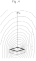
- Fig. 4 shows the magnetic field calculated by electromagnetic field simulations with contour lines. In Fig.
- a point located at a distance of 2 mm in the Z-axis direction from the center of the package of the RFID tag is referred to as P obs
- the magnetic field at the point P obs is calculated every 20 MHz from 715 MHz to 1115 MHz.
- These calculated values are plotted on a graph, with the horizontal axis representing the frequency (GHz) and the vertical axis representing the amplitude (A.U.) of the magnetic field.
- the amplitude of the magnetic field at 915 MHz that is the operating frequency is important, and the larger the value of the amplitude, the more the communication distance is improved.
- the data of the RFID tag 1 are plotted with black dots, and the data of the RFID tag of model 1 as a comparative example are plotted with "+".
- the antenna is disposed in the antenna-forming area between the outer peripheral edges of the insulating layer and the plurality of connection terminals, the aspect ratio is set to 1.25, the line width of the turns of the conductor line 3a that are adjacent to each other in the radial direction is set to 4 ⁇ m, the spacing (so-called line spacing) S between the turns of the conductor line 3a from each other is set to 2.83 pm, and the number of turns is set to 5.75.
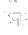
- the antenna is disposed in the antenna-forming area between the outer peripheral edges of the insulating layer and the plurality of connection terminals, the aspect ratio is set to 1.25, the line width of the turns of the conductor line 3a that are adjacent to each other in the radial direction is set to 10 ⁇ m (which is a value out of the range of the present invention), the spacing (so-called line spacing) S between the turns of the conductor line 3a from each other is set to 8 ⁇ m (which is a value out of the range of tag 1), and the number of turns is set to 1.75.
- the reason why the number of turns in the conductor pattern is 1.75 is that, when a conductive material having a line width of 10 ⁇ m is wound once, as shown in Fig. 5B , a distance M between the conductor line 3a and the connection terminal 5B is 25 ⁇ m.
- a conductive material cannot be wounded twice.
- the graph of Fig. 5A shows that, while the size of the magnetic field of the RFID tag 1 at 915 MHz that is the operating frequency is a value over 100 (A.U.), the size of the magnetic field of the RFID tag of model 1 at 915 MHz that is the operating frequency is less than 10 (A.U.), resulting that the communication distance of the RFID tag 1 can be increased as compared with that of the RFID tag of model 1.
- the line width of the conductor line 3a and the spacing between the turns of the conductor line 3a are out of the ranges of the present invention, and it is important that the line width falls within the range of 2 ⁇ m to 7 ⁇ m, and that the spacing between the turns of the conductor line 3a falls within the range of 2 ⁇ m to 7 ⁇ m, as in tag 1.
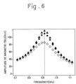
- the data of the RFID tag 1 are plotted with black dots
- the data of the RFID tag 2 having a different specification from the RFID tag 1 are plotted with black triangles
- the data of an RFID tag as a comparative example having a different specification from model 1 are plotted with outlined rhombuses.
- the antenna is disposed in the antenna-forming area between the outer peripheral edges of the insulating layer and the plurality of connection terminals, as described above, the aspect ratio is set to 1.25, the line width of the turns of the conductor line 3a that are adjacent to each other in the radial direction is set to 4 ⁇ m, the spacing (so-called line spacing) S between the turns of the conductor line 3a from each other is set to 2.83 ⁇ m, and the number of turns in the conductor pattern is set to 5.75.
- the antenna is disposed in the antenna-forming area between the outer peripheral edges of the insulating layer and the plurality of connection terminals, in the same manner as in the RFID tag 1, the aspect ratio is set to 2.5 (a value different from that in the tag 1), the line width of the turns of the conductor line 3a that are adjacent to each other in the radial direction is set to 4 pm (the same value as that in the tag 1), the spacing (so-called line spacing) S between the turns of the conductor line 3a from each other is set to 2.29 pm (a value different from that in the tag 1), and the number of turns in the conductor pattern is set to 5.75.
- the antenna is disposed in the antenna-forming area between the outer peripheral edges of the insulating layer and the plurality of connection terminals, in the same manner as in the tag 1, the aspect ratio is set to 0.5, the line width of the turns of the conductor line 3a that are adjacent to each other in the radial direction is set to 4 pm (which is a value within the range of the present invention), the spacing (so-called line spacing) S between the turns of the conductor line 3a from each other is set to 3 ⁇ m, and the number of turns in the conductor pattern is set to 5.75.
- the graph of Fig. 6 shows that, while the size of the magnetic field of the RFID tags 1 and 2 at 915 MHz that is the operating frequency is a value over 100 (A.U.), the size of the magnetic field of the RFID tag of model 2 at 915 MHz that is the operating frequency is nearly 80 (A.U.), resulting that the communication distance of the RFID tags 1 and 2 can be increased as compared with that of the RFID tag of model 2.
- the aspect ratio is out of the range of 1.0 to 5.0, which is the range of the aspect ratio, and it is important that the aspect ratio is set within the range of 1.0 to 5.0.
- the data of the RFID tag 1 are plotted with black dots, and the data of the RFID tag of model 3 as a comparative example are plotted with " ⁇ ".
- the antenna is disposed in the antenna-forming area between the outer peripheral edges of the insulating layer and the plurality of connection terminals, as described above, the aspect ratio is set to 1.25, the line width of the turns of the conductor line 3a that are adjacent to each other in the radial direction is set to 4 pm, the spacing (so-called line spacing) S between the turns of the conductor line 3a from each other is set to 2.83 pm, and the number of turns in the conductor pattern is set to 5.75.
- the antenna is disposed in the antenna-forming area between the outer peripheral edges of the insulating layer and the plurality of connection terminals, the aspect ratio is set to 0.5, the line width of the turns of the conductor line 3a that are adjacent to each other in the radial direction is set to 10 pm, the spacing (so-called line spacing) S between the turns of the conductor line 3a from each other is set to 8 ⁇ m (which is a value out of the range of the present invention), and the number of turns in the conductor pattern is set to 1.75 as in model 1.
- all values of the aspect ratio, the line width of the conductor line 3a, and the spacing between the turns of the conductor line 3a are out of the ranges of the present invention, and it is important that the aspect ratio falls within the range of 1.0 to 5.0, the line width of the conductor line 3a falls within the range of 2 ⁇ m to 7 ⁇ m, and the spacing between the turns of the conductor line falls within the range of 2 ⁇ m to 7 ⁇ m,.
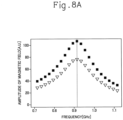
- Fig. 8A the data of the RFID tag 3 having a different specification from the specification of tag 1 and the specification of tag 2 are plotted with black squares, and the data of the RFID tag of model 4 as a comparative example are plotted with outlined downward triangles.
- the antenna is disposed in the antenna-forming area between the outer peripheral edges of the insulating layer and the plurality of connection terminals, as described above, the aspect ratio is set to 1.67 (a value different from the values of tags 1 and 2), the line width of the turns of the conductor line 3a that are adjacent to each other in the radial direction is set to 3 pm (a value different from the values in the tags 1 and 2), the spacing (so-called line spacing) S between the turns of the conductor line 3a from each other is set to 3.9 ⁇ m (a value different from the values of tags 1 and 2), and the number of turns in the conductor pattern is set to 5.75.
- the antenna is disposed to be located in almost half of an antenna-forming area R between the outer peripheral edges of the insulating layer and the two input and output terminals 5A and 5B, as shown in Fig. 8B , the aspect ratio is set to 1.67, the line width of the turns of the conductor line 3a that are adjacent to each other in the radial direction is set to 3 ⁇ m, the spacing (so-called line spacing) S between the turns of the conductor line 3a from each other is set to 2.5 ⁇ m, and the number of turns in the conductor pattern is set to 5.75.
- the graph of Fig. 8A shows that, while the size of the magnetic field of the RFID tag 3 at 915 MHz that is the operating frequency is a value over 100 (A.U.), the size of the magnetic field of the RFID tag of model 4 at 915 MHz that is the operating frequency is nearly 75 (A.U.), resulting that the communication distance of the RFID tag 3 can be increased as compared with that of the RFID tag of model 4. This is considered to be because in the RFID tag of model 4, almost half of the antenna 3 is disposed in an area shifted inwardly out of the antenna-forming area R formed on the outer periphery of the IC chip 1 and therefore the outer diameter dimension of the antenna 3 is reduced.
- the antenna-forming area is formed over substantially the entire periphery of the insulating layer by winding the conductor line 3a inside the input and output terminal 5B so that the conductor line 3a wound inwardly does not overlap itself that is connected to the input and output terminal 5B, but the antenna-forming area may be formed over the entire periphery of the insulating layer by winding it so that the conductor line 3a wound inwardly overlaps itself that is connected to the input and output terminal 5B.
- the insulating layer is formed so that one of the portions of the conductor line 3a is moved upward apart from the other portion and the conductor line 3a that has been moved upward is maintained at the position.
- the antenna is configured by disposing the conductor line 3a into a spiral in parallel, but the antenna that is wound multiple times may be configured by stacking two or more of single layers formed by disposing the conductor line 3a into a loop on the insulating layer.
- the antenna is formed on the upper surface of the package of the IC chip, but the antenna may be formed on a substrate provided to mount the IC chip. Such an embodiment is carried out by providing a plurality of connection terminals for being connected to the IC chip on the substrate.
Landscapes
- Engineering & Computer Science (AREA)
- Microelectronics & Electronic Packaging (AREA)
- Computer Networks & Wireless Communication (AREA)
- Computer Hardware Design (AREA)
- Physics & Mathematics (AREA)
- General Physics & Mathematics (AREA)
- Theoretical Computer Science (AREA)
- Signal Processing (AREA)
- Details Of Aerials (AREA)
- Near-Field Transmission Systems (AREA)
Claims (2)
- Verstärkerantenne (6) für eine spiralförmige Antenne (3), die auf einem IC-Chip (1) vorgesehen ist, wobei die Verstärkerantenne (6) eingerichtet ist, um mit im Wesentlichen der gleichen Frequenz wie eine Betriebsfrequenz der spiralförmigen Antenne (3) betrieben zu werden, wobei die Verstärkerantenne (6) umfasst:eine keramische rechteckige Basis (7);eine Isolierschicht (8), die aus Keramik hergestellt und auf der keramischen rechteckigen Basis (7) gestapelt gebildet ist;ein Leitermuster (9), das in die Keramik der Isolierschicht (8) eingebettet ist, wobei das eine Leitermuster (9) aus einer Leiterbahn (9a) besteht, die spiralförmig gewunden ist, um eine Öffnung (9K) zu bilden; undeine Keramikhalterung (10) zum Montieren des IC-Chips (1), wobei die Keramikhalterung (10) auf der Isolierschicht (8) gestapelt ist und wobei die Keramikhalterung (10) eine Aussparung (10A) aufweist, die in einer Draufsicht rechteckig ist und zum Montieren des IC-Chips (1) eingerichtet ist,wobei das eine Leitermuster (9) eingerichtet ist, um im montierten Zustand auf der Halterung (10) mit der Antenne (3) des IC-Chips (1) elektromagnetisch zur Resonanz gekoppelt zu sein, um dadurch mit im Wesentlichen der gleichen Frequenz wie die Betriebsfrequenz der spiralförmigen Antenne (3) des IC-Chips (1) betrieben zu werden.
- Verstärkerantenne (6) für eine spiralförmige Antenne (3), die auf einem IC-Chip (1) vorgesehen ist, nach Anspruch 1, wobei der IC-Chip (1), der innerhalb der Aussparung (10A) platziert ist, mit einem Harz vergossen ist, das den gleichen oder fast den gleichen Wärmeausdehnungskoeffizienten wie Keramik aufweist.
Applications Claiming Priority (3)
| Application Number | Priority Date | Filing Date | Title |
|---|---|---|---|
| JP2016082202A JP6251770B2 (ja) | 2016-04-15 | 2016-04-15 | Rfidタグ |
| EP17782414.1A EP3444899B1 (de) | 2016-04-15 | 2017-04-12 | Rfid-etikett |
| PCT/JP2017/014913 WO2017179601A1 (ja) | 2016-04-15 | 2017-04-12 | Rfidタグ |
Related Parent Applications (2)
| Application Number | Title | Priority Date | Filing Date |
|---|---|---|---|
| EP17782414.1A Division EP3444899B1 (de) | 2016-04-15 | 2017-04-12 | Rfid-etikett |
| EP17782414.1A Division-Into EP3444899B1 (de) | 2016-04-15 | 2017-04-12 | Rfid-etikett |
Publications (2)
| Publication Number | Publication Date |
|---|---|
| EP3866262A1 EP3866262A1 (de) | 2021-08-18 |
| EP3866262B1 true EP3866262B1 (de) | 2025-01-22 |
Family
ID=60042124
Family Applications (2)
| Application Number | Title | Priority Date | Filing Date |
|---|---|---|---|
| EP21167029.4A Active EP3866262B1 (de) | 2016-04-15 | 2017-04-12 | Rfid-etikett |
| EP17782414.1A Active EP3444899B1 (de) | 2016-04-15 | 2017-04-12 | Rfid-etikett |
Family Applications After (1)
| Application Number | Title | Priority Date | Filing Date |
|---|---|---|---|
| EP17782414.1A Active EP3444899B1 (de) | 2016-04-15 | 2017-04-12 | Rfid-etikett |
Country Status (6)
| Country | Link |
|---|---|
| US (1) | US10528859B2 (de) |
| EP (2) | EP3866262B1 (de) |
| JP (1) | JP6251770B2 (de) |
| CN (2) | CN109075447B (de) |
| TW (2) | TWI690116B (de) |
| WO (1) | WO2017179601A1 (de) |
Families Citing this family (8)
| Publication number | Priority date | Publication date | Assignee | Title |
|---|---|---|---|---|
| GB2491447B (en) * | 2010-03-24 | 2014-10-22 | Murata Manufacturing Co | RFID system |
| TWI671682B (zh) * | 2018-03-06 | 2019-09-11 | 劉台華 | 耐高溫rfid標籤 |
| US11809939B2 (en) * | 2019-03-29 | 2023-11-07 | Kyocera Corporation | RFID tag with boost antenna, conductor provided with RFID tag with boost antenna, and RFID system including RFID tag with boost antenna |
| JP6546711B1 (ja) | 2019-04-10 | 2019-07-17 | 株式会社エスケーエレクトロニクス | 非接触情報担体 |
| TWI706596B (zh) * | 2019-09-16 | 2020-10-01 | 安諾電子股份有限公司 | 包含導電環狀結構以改善效能之天線裝置 |
| JP7389327B2 (ja) * | 2019-09-20 | 2023-11-30 | 横浜ゴム株式会社 | マリンホースの流体漏れ検知システム |
| USD1032613S1 (en) * | 2020-02-02 | 2024-06-25 | Federal Card Services, LLC | Smart card |
| TWI803957B (zh) * | 2021-09-01 | 2023-06-01 | 韋僑科技股份有限公司 | 無線射頻晶片模組及其rfid接收器 |
Family Cites Families (36)
| Publication number | Priority date | Publication date | Assignee | Title |
|---|---|---|---|---|
| JP4363735B2 (ja) * | 1999-02-24 | 2009-11-11 | 日立マクセル株式会社 | 情報担体の製造方法 |
| DE60014377T2 (de) | 1999-02-24 | 2006-03-02 | Hitachi Maxell, Ltd., Ibaraki | Integrierte schaltung und ihre herstellung, und auf einem informationsträger montierte integrierte schaltung |
| JP4641096B2 (ja) * | 2000-12-07 | 2011-03-02 | 大日本印刷株式会社 | 非接触式データキャリア装置とブースターアンテナ部用配線部材 |
| JP4690561B2 (ja) * | 2001-01-24 | 2011-06-01 | 日立マクセル株式会社 | 半導体チップ |
| JP4141857B2 (ja) * | 2003-02-18 | 2008-08-27 | 日立マクセル株式会社 | 半導体装置 |
| JP2004280627A (ja) * | 2003-03-18 | 2004-10-07 | Hitachi Maxell Ltd | 半導体装置 |
| JP4209230B2 (ja) * | 2003-03-24 | 2009-01-14 | トッパン・フォームズ株式会社 | 共振タグおよび非接触型データ受送信体 |
| JP4572532B2 (ja) * | 2003-11-20 | 2010-11-04 | セイコーエプソン株式会社 | 電気泳動表示装置及び非接触通信媒体 |
| US7405665B2 (en) * | 2003-12-19 | 2008-07-29 | Semiconductor Energy Laboratory Co., Ltd. | Semiconductor device, RFID tag and label-like object |
| FR2899000B1 (fr) * | 2006-03-24 | 2008-10-17 | Arjowiggins Security Soc Par A | Dispositif radiofrequence comportant un composant electronique pourvu d'une antenne integree et couplee electromagnetiquement a une antenne d'amplification |
| US8816484B2 (en) * | 2007-02-09 | 2014-08-26 | Semiconductor Energy Laboratory Co., Ltd. | Semiconductor device |
| JP2008226070A (ja) * | 2007-03-15 | 2008-09-25 | Dainippon Printing Co Ltd | 絶縁性金属光沢層付き非接触icタグ |
| EP2019425A1 (de) * | 2007-07-27 | 2009-01-28 | Semiconductor Energy Laboratory Co., Ltd. | Halbleiterbauelement und Verfahren zu seiner Herstellung |
| JP4890386B2 (ja) * | 2007-08-20 | 2012-03-07 | アルプス電気株式会社 | アンテナコイル |
| JP2009093507A (ja) * | 2007-10-11 | 2009-04-30 | Hitachi Ltd | Rfidタグ |
| JP2009290829A (ja) * | 2008-06-02 | 2009-12-10 | Alps Electric Co Ltd | ループアンテナ装置 |
| JP4713621B2 (ja) | 2008-09-12 | 2011-06-29 | 株式会社エフ・イー・シー | アンテナ搭載形の通信用icユニット |
| CN201303050Y (zh) * | 2008-10-16 | 2009-09-02 | 上海集成电路研发中心有限公司 | 应用于rfid芯片的集成天线 |
| CN101447603A (zh) * | 2008-12-19 | 2009-06-03 | 上海集成电路研发中心有限公司 | 一种rfid芯片上的具有渐进式结构的天线 |
| KR20110008478A (ko) * | 2009-07-20 | 2011-01-27 | 엘지전자 주식회사 | Rfid 안테나와 이를 이용한 이동 단말기 |
| JP5376060B2 (ja) * | 2010-07-08 | 2013-12-25 | 株式会社村田製作所 | アンテナ及びrfidデバイス |
| WO2013020971A1 (en) * | 2011-08-08 | 2013-02-14 | Féinics Amatech Teoranta | Improving coupling in and to rfid smart cards |
| KR101374302B1 (ko) * | 2011-02-15 | 2014-03-14 | 가부시키가이샤 무라타 세이사쿠쇼 | 안테나 장치 및 통신단말장치 |
| JP5293907B2 (ja) * | 2011-06-13 | 2013-09-18 | 株式会社村田製作所 | アンテナ装置および通信端末装置 |
| WO2013035821A1 (ja) * | 2011-09-09 | 2013-03-14 | 株式会社村田製作所 | アンテナ装置および無線デバイス |
| WO2013073314A1 (ja) * | 2011-11-14 | 2013-05-23 | 株式会社村田製作所 | アンテナ装置及び無線通信装置 |
| EP2988254B1 (de) * | 2011-11-17 | 2018-10-03 | Toppan Printing Co., Ltd. | Komposit ic-karte |
| WO2013094667A1 (ja) * | 2011-12-22 | 2013-06-27 | 株式会社村田製作所 | 磁性体アンテナ、アンテナ装置及び電子機器 |
| WO2013115158A1 (ja) * | 2012-02-01 | 2013-08-08 | 株式会社村田製作所 | アンテナ装置および無線通信装置 |
| JP5464307B2 (ja) * | 2012-02-24 | 2014-04-09 | 株式会社村田製作所 | アンテナ装置および無線通信装置 |
| WO2013183575A1 (ja) * | 2012-06-04 | 2013-12-12 | 株式会社村田製作所 | アンテナ装置および無線通信装置 |
| JP5672414B2 (ja) * | 2012-10-12 | 2015-02-18 | 株式会社村田製作所 | Hf帯無線通信デバイス |
| CN204242218U (zh) * | 2012-12-07 | 2015-04-01 | 株式会社村田制作所 | 天线模块 |
| JP2015064651A (ja) * | 2013-09-24 | 2015-04-09 | 日立化成株式会社 | Rfidタグ及び自動認識システム |
| WO2016031311A1 (ja) * | 2014-08-27 | 2016-03-03 | 株式会社村田製作所 | コイルアンテナ、無線icデバイスおよびコイルアンテナの製造方法 |
| JP6008069B1 (ja) * | 2015-03-06 | 2016-10-19 | 株式会社村田製作所 | 無線icデバイス、それを備えた樹脂成型体、それを備えた通信端末装置、及びその製造方法 |
-
2016
- 2016-04-15 JP JP2016082202A patent/JP6251770B2/ja active Active
-
2017
- 2017-04-12 CN CN201780023194.9A patent/CN109075447B/zh active Active
- 2017-04-12 CN CN202110686528.9A patent/CN113487002B/zh active Active
- 2017-04-12 US US16/093,697 patent/US10528859B2/en active Active
- 2017-04-12 EP EP21167029.4A patent/EP3866262B1/de active Active
- 2017-04-12 WO PCT/JP2017/014913 patent/WO2017179601A1/ja not_active Ceased
- 2017-04-12 EP EP17782414.1A patent/EP3444899B1/de active Active
- 2017-04-13 TW TW107146452A patent/TWI690116B/zh active
- 2017-04-13 TW TW106112321A patent/TWI651886B/zh active
Also Published As
| Publication number | Publication date |
|---|---|
| JP2017192109A (ja) | 2017-10-19 |
| EP3866262A1 (de) | 2021-08-18 |
| CN109075447B (zh) | 2021-06-29 |
| EP3444899A4 (de) | 2019-12-04 |
| CN113487002B (zh) | 2024-11-26 |
| HK1259475A1 (zh) | 2019-11-29 |
| TWI651886B (zh) | 2019-02-21 |
| US10528859B2 (en) | 2020-01-07 |
| CN113487002A (zh) | 2021-10-08 |
| US20190080215A1 (en) | 2019-03-14 |
| JP6251770B2 (ja) | 2017-12-20 |
| TW201921799A (zh) | 2019-06-01 |
| WO2017179601A1 (ja) | 2017-10-19 |
| TWI690116B (zh) | 2020-04-01 |
| TW201739102A (zh) | 2017-11-01 |
| CN109075447A (zh) | 2018-12-21 |
| EP3444899B1 (de) | 2021-06-09 |
| EP3444899A1 (de) | 2019-02-20 |
Similar Documents
| Publication | Publication Date | Title |
|---|---|---|
| EP3866262B1 (de) | Rfid-etikett | |
| US10013650B2 (en) | Wireless communication module and wireless communication device | |
| KR101850806B1 (ko) | 안테나 | |
| US8668151B2 (en) | Wireless IC device | |
| US8602310B2 (en) | Radio communication device and radio communication terminal | |
| US8937576B2 (en) | Wireless communication device | |
| CN103782446B (zh) | 天线装置及无线通信装置 | |
| US10396429B2 (en) | Wireless communication device | |
| US10476147B2 (en) | Antenna device and method of manufacturing the same | |
| US20150188227A1 (en) | Antenna for near field communication, antenna arrangement, transponder with antenna, flat panel and methods of manufacturing | |
| JP5724671B2 (ja) | アンテナ装置、rfidタグおよび通信端末装置 | |
| CN205621840U (zh) | 天线装置 | |
| JP6789202B2 (ja) | ブースターアンテナ | |
| KR100862890B1 (ko) | Rfid 안테나 회로 장치 및 이를 포함하는 rfid카드 | |
| JP2008244740A (ja) | 改良された範囲を持つrfidタグ | |
| EP1970993B1 (de) | RFID-Chip und Antenne mit verbessertem Bereich | |
| HK40058006A (en) | Gaining antenna | |
| EP1970840A1 (de) | RFID-Etikett mit verbessertem Bereich | |
| TWI803957B (zh) | 無線射頻晶片模組及其rfid接收器 | |
| HK1259475B (zh) | Rfid标签 | |
| HK40058006B (zh) | 增益天线 |
Legal Events
| Date | Code | Title | Description |
|---|---|---|---|
| PUAI | Public reference made under article 153(3) epc to a published international application that has entered the european phase |
Free format text: ORIGINAL CODE: 0009012 |
|
| STAA | Information on the status of an ep patent application or granted ep patent |
Free format text: STATUS: THE APPLICATION HAS BEEN PUBLISHED |
|
| AC | Divisional application: reference to earlier application |
Ref document number: 3444899 Country of ref document: EP Kind code of ref document: P |
|
| AK | Designated contracting states |
Kind code of ref document: A1 Designated state(s): AL AT BE BG CH CY CZ DE DK EE ES FI FR GB GR HR HU IE IS IT LI LT LU LV MC MK MT NL NO PL PT RO RS SE SI SK SM TR |
|
| STAA | Information on the status of an ep patent application or granted ep patent |
Free format text: STATUS: REQUEST FOR EXAMINATION WAS MADE |
|
| 17P | Request for examination filed |
Effective date: 20220211 |
|
| RBV | Designated contracting states (corrected) |
Designated state(s): AL AT BE BG CH CY CZ DE DK EE ES FI FR GB GR HR HU IE IS IT LI LT LU LV MC MK MT NL NO PL PT RO RS SE SI SK SM TR |
|
| STAA | Information on the status of an ep patent application or granted ep patent |
Free format text: STATUS: EXAMINATION IS IN PROGRESS |
|
| 17Q | First examination report despatched |
Effective date: 20221108 |
|
| REG | Reference to a national code |
Ref country code: DE Ref legal event code: R079 Free format text: PREVIOUS MAIN CLASS: H01Q0007000000 Ipc: H04B0005480000 Ref country code: DE Ref legal event code: R079 Ref document number: 602017087512 Country of ref document: DE Free format text: PREVIOUS MAIN CLASS: H01Q0007000000 Ipc: H04B0005480000 |
|
| GRAP | Despatch of communication of intention to grant a patent |
Free format text: ORIGINAL CODE: EPIDOSNIGR1 |
|
| STAA | Information on the status of an ep patent application or granted ep patent |
Free format text: STATUS: GRANT OF PATENT IS INTENDED |
|
| RIC1 | Information provided on ipc code assigned before grant |
Ipc: G06K 19/077 20060101ALI20240820BHEP Ipc: H01Q 7/00 20060101ALI20240820BHEP Ipc: H04B 5/48 20240101AFI20240820BHEP |
|
| INTG | Intention to grant announced |
Effective date: 20240830 |
|
| GRAS | Grant fee paid |
Free format text: ORIGINAL CODE: EPIDOSNIGR3 |
|
| GRAA | (expected) grant |
Free format text: ORIGINAL CODE: 0009210 |
|
| STAA | Information on the status of an ep patent application or granted ep patent |
Free format text: STATUS: THE PATENT HAS BEEN GRANTED |
|
| AC | Divisional application: reference to earlier application |
Ref document number: 3444899 Country of ref document: EP Kind code of ref document: P |
|
| AK | Designated contracting states |
Kind code of ref document: B1 Designated state(s): AL AT BE BG CH CY CZ DE DK EE ES FI FR GB GR HR HU IE IS IT LI LT LU LV MC MK MT NL NO PL PT RO RS SE SI SK SM TR |
|
| REG | Reference to a national code |
Ref country code: GB Ref legal event code: FG4D |
|
| REG | Reference to a national code |
Ref country code: CH Ref legal event code: EP |
|
| REG | Reference to a national code |
Ref country code: IE Ref legal event code: FG4D |
|
| REG | Reference to a national code |
Ref country code: DE Ref legal event code: R096 Ref document number: 602017087512 Country of ref document: DE |
|
| REG | Reference to a national code |
Ref country code: NL Ref legal event code: MP Effective date: 20250122 |
|
| PG25 | Lapsed in a contracting state [announced via postgrant information from national office to epo] |
Ref country code: NL Free format text: LAPSE BECAUSE OF FAILURE TO SUBMIT A TRANSLATION OF THE DESCRIPTION OR TO PAY THE FEE WITHIN THE PRESCRIBED TIME-LIMIT Effective date: 20250122 |
|
| PG25 | Lapsed in a contracting state [announced via postgrant information from national office to epo] |
Ref country code: RS Free format text: LAPSE BECAUSE OF FAILURE TO SUBMIT A TRANSLATION OF THE DESCRIPTION OR TO PAY THE FEE WITHIN THE PRESCRIBED TIME-LIMIT Effective date: 20250422 |
|
| PG25 | Lapsed in a contracting state [announced via postgrant information from national office to epo] |
Ref country code: FI Free format text: LAPSE BECAUSE OF FAILURE TO SUBMIT A TRANSLATION OF THE DESCRIPTION OR TO PAY THE FEE WITHIN THE PRESCRIBED TIME-LIMIT Effective date: 20250122 |
|
| PG25 | Lapsed in a contracting state [announced via postgrant information from national office to epo] |
Ref country code: PL Free format text: LAPSE BECAUSE OF FAILURE TO SUBMIT A TRANSLATION OF THE DESCRIPTION OR TO PAY THE FEE WITHIN THE PRESCRIBED TIME-LIMIT Effective date: 20250122 |
|
| PGFP | Annual fee paid to national office [announced via postgrant information from national office to epo] |
Ref country code: DE Payment date: 20250430 Year of fee payment: 9 |
|
| PG25 | Lapsed in a contracting state [announced via postgrant information from national office to epo] |
Ref country code: ES Free format text: LAPSE BECAUSE OF FAILURE TO SUBMIT A TRANSLATION OF THE DESCRIPTION OR TO PAY THE FEE WITHIN THE PRESCRIBED TIME-LIMIT Effective date: 20250122 |
|
| PGFP | Annual fee paid to national office [announced via postgrant information from national office to epo] |
Ref country code: GB Payment date: 20250423 Year of fee payment: 9 |
|
| REG | Reference to a national code |
Ref country code: LT Ref legal event code: MG9D |
|
| PG25 | Lapsed in a contracting state [announced via postgrant information from national office to epo] |
Ref country code: NO Free format text: LAPSE BECAUSE OF FAILURE TO SUBMIT A TRANSLATION OF THE DESCRIPTION OR TO PAY THE FEE WITHIN THE PRESCRIBED TIME-LIMIT Effective date: 20250422 Ref country code: IS Free format text: LAPSE BECAUSE OF FAILURE TO SUBMIT A TRANSLATION OF THE DESCRIPTION OR TO PAY THE FEE WITHIN THE PRESCRIBED TIME-LIMIT Effective date: 20250522 |
|
| REG | Reference to a national code |
Ref country code: AT Ref legal event code: MK05 Ref document number: 1762235 Country of ref document: AT Kind code of ref document: T Effective date: 20250122 |
|
| PG25 | Lapsed in a contracting state [announced via postgrant information from national office to epo] |
Ref country code: HR Free format text: LAPSE BECAUSE OF FAILURE TO SUBMIT A TRANSLATION OF THE DESCRIPTION OR TO PAY THE FEE WITHIN THE PRESCRIBED TIME-LIMIT Effective date: 20250122 |
|
| PG25 | Lapsed in a contracting state [announced via postgrant information from national office to epo] |
Ref country code: PT Free format text: LAPSE BECAUSE OF FAILURE TO SUBMIT A TRANSLATION OF THE DESCRIPTION OR TO PAY THE FEE WITHIN THE PRESCRIBED TIME-LIMIT Effective date: 20250522 Ref country code: LV Free format text: LAPSE BECAUSE OF FAILURE TO SUBMIT A TRANSLATION OF THE DESCRIPTION OR TO PAY THE FEE WITHIN THE PRESCRIBED TIME-LIMIT Effective date: 20250122 |
|
| PGFP | Annual fee paid to national office [announced via postgrant information from national office to epo] |
Ref country code: FR Payment date: 20250425 Year of fee payment: 9 |
|
| PG25 | Lapsed in a contracting state [announced via postgrant information from national office to epo] |
Ref country code: BG Free format text: LAPSE BECAUSE OF FAILURE TO SUBMIT A TRANSLATION OF THE DESCRIPTION OR TO PAY THE FEE WITHIN THE PRESCRIBED TIME-LIMIT Effective date: 20250122 Ref country code: GR Free format text: LAPSE BECAUSE OF FAILURE TO SUBMIT A TRANSLATION OF THE DESCRIPTION OR TO PAY THE FEE WITHIN THE PRESCRIBED TIME-LIMIT Effective date: 20250423 |
|
| PG25 | Lapsed in a contracting state [announced via postgrant information from national office to epo] |
Ref country code: AT Free format text: LAPSE BECAUSE OF FAILURE TO SUBMIT A TRANSLATION OF THE DESCRIPTION OR TO PAY THE FEE WITHIN THE PRESCRIBED TIME-LIMIT Effective date: 20250122 |
|
| PG25 | Lapsed in a contracting state [announced via postgrant information from national office to epo] |
Ref country code: SE Free format text: LAPSE BECAUSE OF FAILURE TO SUBMIT A TRANSLATION OF THE DESCRIPTION OR TO PAY THE FEE WITHIN THE PRESCRIBED TIME-LIMIT Effective date: 20250122 |
|
| PG25 | Lapsed in a contracting state [announced via postgrant information from national office to epo] |
Ref country code: SM Free format text: LAPSE BECAUSE OF FAILURE TO SUBMIT A TRANSLATION OF THE DESCRIPTION OR TO PAY THE FEE WITHIN THE PRESCRIBED TIME-LIMIT Effective date: 20250122 |
|
| PG25 | Lapsed in a contracting state [announced via postgrant information from national office to epo] |
Ref country code: DK Free format text: LAPSE BECAUSE OF FAILURE TO SUBMIT A TRANSLATION OF THE DESCRIPTION OR TO PAY THE FEE WITHIN THE PRESCRIBED TIME-LIMIT Effective date: 20250122 |
|
| PG25 | Lapsed in a contracting state [announced via postgrant information from national office to epo] |
Ref country code: IT Free format text: LAPSE BECAUSE OF FAILURE TO SUBMIT A TRANSLATION OF THE DESCRIPTION OR TO PAY THE FEE WITHIN THE PRESCRIBED TIME-LIMIT Effective date: 20250122 |
|
| PG25 | Lapsed in a contracting state [announced via postgrant information from national office to epo] |
Ref country code: CZ Free format text: LAPSE BECAUSE OF FAILURE TO SUBMIT A TRANSLATION OF THE DESCRIPTION OR TO PAY THE FEE WITHIN THE PRESCRIBED TIME-LIMIT Effective date: 20250122 Ref country code: EE Free format text: LAPSE BECAUSE OF FAILURE TO SUBMIT A TRANSLATION OF THE DESCRIPTION OR TO PAY THE FEE WITHIN THE PRESCRIBED TIME-LIMIT Effective date: 20250122 |
|
| REG | Reference to a national code |
Ref country code: DE Ref legal event code: R097 Ref document number: 602017087512 Country of ref document: DE |
|
| PG25 | Lapsed in a contracting state [announced via postgrant information from national office to epo] |
Ref country code: RO Free format text: LAPSE BECAUSE OF FAILURE TO SUBMIT A TRANSLATION OF THE DESCRIPTION OR TO PAY THE FEE WITHIN THE PRESCRIBED TIME-LIMIT Effective date: 20250122 |
|
| PG25 | Lapsed in a contracting state [announced via postgrant information from national office to epo] |
Ref country code: SK Free format text: LAPSE BECAUSE OF FAILURE TO SUBMIT A TRANSLATION OF THE DESCRIPTION OR TO PAY THE FEE WITHIN THE PRESCRIBED TIME-LIMIT Effective date: 20250122 |
|
| REG | Reference to a national code |
Ref country code: CH Ref legal event code: H13 Free format text: ST27 STATUS EVENT CODE: U-0-0-H10-H13 (AS PROVIDED BY THE NATIONAL OFFICE) Effective date: 20251125 |
|
| PLBE | No opposition filed within time limit |
Free format text: ORIGINAL CODE: 0009261 |
|
| STAA | Information on the status of an ep patent application or granted ep patent |
Free format text: STATUS: NO OPPOSITION FILED WITHIN TIME LIMIT |
|
| PG25 | Lapsed in a contracting state [announced via postgrant information from national office to epo] |
Ref country code: LU Free format text: LAPSE BECAUSE OF NON-PAYMENT OF DUE FEES Effective date: 20250412 |
|
| PG25 | Lapsed in a contracting state [announced via postgrant information from national office to epo] |
Ref country code: MC Free format text: LAPSE BECAUSE OF FAILURE TO SUBMIT A TRANSLATION OF THE DESCRIPTION OR TO PAY THE FEE WITHIN THE PRESCRIBED TIME-LIMIT Effective date: 20250122 |
|
| REG | Reference to a national code |
Ref country code: BE Ref legal event code: MM Effective date: 20250430 |
|
| 26N | No opposition filed |
Effective date: 20251023 |
|
| PG25 | Lapsed in a contracting state [announced via postgrant information from national office to epo] |
Ref country code: BE Free format text: LAPSE BECAUSE OF NON-PAYMENT OF DUE FEES Effective date: 20250430 |
|
| PG25 | Lapsed in a contracting state [announced via postgrant information from national office to epo] |
Ref country code: CH Free format text: LAPSE BECAUSE OF NON-PAYMENT OF DUE FEES Effective date: 20250430 |