EP3813115B1 - Lichtempfindliche chipgehäusestruktur, kameramodul und mobiles endgerät - Google Patents
Lichtempfindliche chipgehäusestruktur, kameramodul und mobiles endgerät Download PDFInfo
- Publication number
- EP3813115B1 EP3813115B1 EP18931620.1A EP18931620A EP3813115B1 EP 3813115 B1 EP3813115 B1 EP 3813115B1 EP 18931620 A EP18931620 A EP 18931620A EP 3813115 B1 EP3813115 B1 EP 3813115B1
- Authority
- EP
- European Patent Office
- Prior art keywords
- photosensitive chip
- frame
- retaining wall
- photosensitive
- package structure
- Prior art date
- Legal status (The legal status is an assumption and is not a legal conclusion. Google has not performed a legal analysis and makes no representation as to the accuracy of the status listed.)
- Active
Links
Images



Classifications
-
- H—ELECTRICITY
- H10—SEMICONDUCTOR DEVICES; ELECTRIC SOLID-STATE DEVICES NOT OTHERWISE PROVIDED FOR
- H10F—INORGANIC SEMICONDUCTOR DEVICES SENSITIVE TO INFRARED RADIATION, LIGHT, ELECTROMAGNETIC RADIATION OF SHORTER WAVELENGTH OR CORPUSCULAR RADIATION
- H10F39/00—Integrated devices, or assemblies of multiple devices, comprising at least one element covered by group H10F30/00, e.g. radiation detectors comprising photodiode arrays
- H10F39/80—Constructional details of image sensors
- H10F39/804—Containers or encapsulations
-
- H—ELECTRICITY
- H04—ELECTRIC COMMUNICATION TECHNIQUE
- H04N—PICTORIAL COMMUNICATION, e.g. TELEVISION
- H04N23/00—Cameras or camera modules comprising electronic image sensors; Control thereof
- H04N23/50—Constructional details
- H04N23/54—Mounting of pick-up tubes, electronic image sensors, deviation or focusing coils
-
- H—ELECTRICITY
- H10—SEMICONDUCTOR DEVICES; ELECTRIC SOLID-STATE DEVICES NOT OTHERWISE PROVIDED FOR
- H10F—INORGANIC SEMICONDUCTOR DEVICES SENSITIVE TO INFRARED RADIATION, LIGHT, ELECTROMAGNETIC RADIATION OF SHORTER WAVELENGTH OR CORPUSCULAR RADIATION
- H10F39/00—Integrated devices, or assemblies of multiple devices, comprising at least one element covered by group H10F30/00, e.g. radiation detectors comprising photodiode arrays
- H10F39/80—Constructional details of image sensors
- H10F39/806—Optical elements or arrangements associated with the image sensors
-
- H—ELECTRICITY
- H10—SEMICONDUCTOR DEVICES; ELECTRIC SOLID-STATE DEVICES NOT OTHERWISE PROVIDED FOR
- H10F—INORGANIC SEMICONDUCTOR DEVICES SENSITIVE TO INFRARED RADIATION, LIGHT, ELECTROMAGNETIC RADIATION OF SHORTER WAVELENGTH OR CORPUSCULAR RADIATION
- H10F39/00—Integrated devices, or assemblies of multiple devices, comprising at least one element covered by group H10F30/00, e.g. radiation detectors comprising photodiode arrays
- H10F39/80—Constructional details of image sensors
- H10F39/811—Interconnections
Definitions
- This application relates to the technical field of electronic devices, and in particular, to a photosensitive chip package structure, a camera module, and a mobile terminal.
- a camera module With continuous advancement of mobile phone miniaturization and ultra-thin design, a mobile phone component is also facing a severe challenge of miniaturization development. As an important module component of a mobile phone, a camera module needs to be further reduced in size to meet a current development need.
- a conventional camera module includes a circuit board 01, a photosensitive chip 02 disposed on the circuit board 01, a package cover 03, an optical filter 04, a voice coil motor 05, and a camera 06.
- a signal pin 011 and a surface-mount device 012 such as a capacitor and a resistor are disposed on an area of the circuit board 01 that avoids the photosensitive chip 02.
- a side of the photosensitive chip 02 that faces away from the circuit board 01 has a photosensitive area and a non-photosensitive area surrounding the photosensitive area.
- a pad 021 is disposed on the non-photosensitive area.
- the pad 021 of the photosensitive chip 02 and the signal pin 011 of the circuit board 01 are connected by a metal wire 07 extending from the non-photosensitive area of the photosensitive chip 02 to the circuit board 01.
- the package cover 03 is disposed over the photosensitive chip 02, the metal wire 07, and the surface-mount device 012.
- a sidewall of the package cover is bonded to the circuit board 01.
- a light-transmitting aperture is disposed at a position on the package cover 03 and opposite to the photosensitive area of the photosensitive chip 02.
- the optical filter 04, the voice coil motor 05, and the camera 06 are sequentially disposed on a side of the package cover 03 away from the circuit board 01, and the optical filter 04 is disposed at a position opposite to the light-transmitting aperture of the package cover 03.
- WO 2011/055508 A1 discloses a radiation detector comprising a radiation sensitive semiconductor layer, a substrate, a pixel electrode, and a frame.
- CN 207 706 274 U relates to a camera module including image sensor chip, frame, and mirror cartridge module.
- CN 102 117 817 A discloses a ultrathin packaging structure of an image sensing chip, comprising a base plate, an image sensing chip, a support and a light transmission layer.
- This application provides a photosensitive chip package structure, a camera module, and a mobile terminal, to reduce a size of the camera module and facilitate miniaturization development.
- this application provides a photosensitive chip package structure, where the photosensitive chip package structure includes a substrate, a photosensitive chip, and a frame.
- the photosensitive chip is mounted on the substrate, and the frame is disposed on a side of the photosensitive chip facing away from the substrate.
- the photosensitive chip has a photosensitive area and a non-photosensitive area, where the non-photosensitive area is disposed around the photosensitive area.
- the photosensitive chip and the substrate are electrically connected by a metal wire.
- a pad is disposed on the non-photosensitive area of the photosensitive chip
- a signal pin is disposed on the substrate, and two ends of the metal wire are respectively connected to the pad and the signal pin.
- the metal wire extends from the non-photosensitive area of the photosensitive chip to the substrate.
- an avoidance groove is disposed on the frame to avoid the metal wire.
- the avoidance groove extends along a side edge of the frame.
- An inner wall of the avoidance groove is an arc-shaped inner wall.
- the avoidance groove is filled with filling glue inside.
- the filling glue can wrap around the metal wire, so that the metal wire is protected.
- the filling glue can be used to bond the frame to the substrate and the non-photosensitive area of the photosensitive chip, so that the frame is supported and is relatively fastened to the photosensitive chip and the substrate.
- the filling glue is filled in the avoidance groove to wrap around the metal wire and bond the frame to the photosensitive chip and the substrate.
- the photosensitive chip is sealed on the side, and a cured filling glue can further support the frame.
- the filling glue filled in the avoidance groove can achieve a function of a sidewall in the current technology, and there is no need to reserve space for mounting the sidewall on the side of the substrate. Therefore, this can significantly reduce a size of the substrate, so that a purpose of reducing the size of the camera module is achieved.
- the arc-shaped inner wall of the avoidance groove can prevent air bubbles from being generated when the filling glue is being filled in, so that the filling glue within the avoidance groove has a better filling effect, overflow of the filling glue is avoided during assembling, the supporting effect of the cured filling glue is improved, and structural stability of the photosensitive chip package structure is improved.
- the frame has a light-transmitting aperture that is disposed at a position opposite to the photosensitive area of the photosensitive chip, so that light can pass through the light-transmitting aperture to irradiate the photosensitive area of the photosensitive chip.
- the photosensitive chip package structure further includes an optical filter, where the optical filter is disposed on the frame at a position opposite to the light-transmitting aperture.
- the frame can be designed into a different structure based on a specific location of the optical filter in the frame.
- the optical filter is disposed on a side of the frame facing away from the photosensitive chip.
- a countersink is disposed on the side of the frame facing away from the photosensitive chip, and the countersink can form an annular step structure with the light-transmitting aperture, so that the optical filter can be fastened to the annular step structure. This reduces a distance between the optical filter and the photosensitive chip, and therefore, a purpose of reducing the height of the camera module is achieved.
- a depth of the countersink is not less than a thickness of the optical filter. Therefore, when the optical filter is fastened to the annular step structure, the optical filter does not extend beyond a surface of the side of the frame facing away from the photosensitive chip. This further reduces the height of the camera module.
- the optical filter is disposed on a side of the frame facing the photosensitive chip. This further reduces a thickness of the frame.
- a voice coil motor is mounted on the side of the frame facing away from the photosensitive chip, the area on the frame that acts as a support is actually an area around the light-transmitting aperture. Therefore, a size of the voice coil motor needs to be larger than a size of the light-transmitting aperture, so that a smaller voice coil motor can be mounted on the frame. This further helps to reduce the size of the camera module.
- the frame has a first retaining wall and a second retaining wall, where the first retaining wall and the second retaining wall are respectively disposed on two sides of the avoidance groove to limit the filling glue as much as possible within the avoidance groove.
- the first retaining wall is located on a side of the avoidance groove that is close to the photosensitive area.
- a sidewall of the optical filter is used to form an inner sidewall of the first retaining wall. This simplifies a structure of the frame and reduces the thickness of the frame.
- an angle formed between the inner sidewall of the first retaining wall and the lower surface of the first retaining wall is an obtuse angle. This helps the filling glue better wrap around the metal wire.
- an inner sidewall of the second retaining wall includes a first arc-shaped surface and a second arc-shaped surface, where the first arc-shaped surface is connected to the lower surface of the second retaining wall and the second arc-shaped surface is connected to a bottom wall of the avoidance groove.
- the first arc-shaped surface protrudes toward the interior of the avoidance groove, and the second arc-shaped surface protrudes backward the interior of the avoidance groove.
- a radius of the first arc-shaped surface is greater than a radius of the second arc-shaped surface.
- a plane of a side, of the substrate, on which the photosensitive chip is mounted is a preset first plane.
- a width of a projection of the first arc-shaped surface in the first plane is greater than a width of a projection of the second arc-shaped surface in the first plane.
- the inner sidewall of the second retaining wall includes a first end and a second end, where the first end is a connection end between the inner sidewall of the second retaining wall and the lower surface of the second retaining wall, and the second end is a connection end between the inner sidewall of the second retaining wall and the bottom wall of the avoidance groove.
- an angle formed by the lower surface of the second retaining wall and a line between the first end and the second end is an obtuse angle.
- the avoidance groove can be disposed along one, two, or three edges of the frame.
- the photosensitive area of the photosensitive chip can be sealed by the filling glue.
- the frame On a side of the frame where the avoidance groove is not disposed, the frame has a sidewall connected to the substrate. The photosensitive area of the photosensitive chip can be sealed by the sidewall. In other words, in this solution, the filling glue and the sidewall together seal the photosensitive area of the photosensitive chip.
- the avoidance groove is disposed along four edges of the frame, and the avoidance groove is of a ring-shaped structure. In this way, the photosensitive area of the photosensitive chip can be packaged by the filling glue filled in the avoidance groove.
- a flange is further disposed on the frame.
- the flange can cover the surface-mount device to protect the surface-mount device.
- the frame further includes a support pin, where one end of the support pin is connected to the substrate, and the other end of the support pin is connected to the frame, so as to support the frame.
- the frame is fabricated using an epoxy molding process, so that good flatness and structural strength can be obtained.
- this application further provides a camera module, where the camera module includes the photosensitive chip package structure according to any of the foregoing implementations.
- the camera module has a relatively small size.
- this application further provides a mobile terminal.
- the mobile terminal includes the foregoing camera module. Because a size of the camera module is reduced, it is easier to realize miniaturization and ultra-thin design of the mobile terminal.
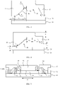
- a photosensitive chip package structure provided in an embodiment of this application includes a substrate 10 and a photosensitive chip 20, where the photosensitive chip 20 is mounted on the substrate 10.
- the photosensitive chip 20 On a side of the photosensitive chip 20 facing away from the substrate 10, the photosensitive chip 20 has a photosensitive area 21 and a non-photosensitive area 22 surrounding the photosensitive area 21.
- a pad 23 is disposed on the non-photosensitive area 22 of the photosensitive chip 20.
- a signal pin 11 is disposed on an area of the substrate 10 that avoids the photosensitive chip 20.
- the pad 23 and the signal pin 11 are connected by a metal wire 30 extending from the non-photosensitive area 22 of the photosensitive chip 20 to the substrate 10.
- the pad 23 or the signal pin 11 may be disposed along one, two, three, or four edges of the photosensitive chip 20.
- the metal wire 30 may also be disposed along one, two, three, or four edges of the photosensitive chip 20.
- the photosensitive chip package structure of this embodiment of this application also includes a frame 40 disposed on a side of the photosensitive chip 20 facing away from the substrate 10.
- the frame 40 is fabricated using an epoxy molding process, so that good flatness and structural strength can be obtained.
- an avoidance groove 41 is disposed on the frame 40 to avoid the metal wire 30.
- the avoidance groove 41 extends along a side edge of the frame 40.
- An inner wall of the avoidance groove 41 is an arc-shaped inner wall.
- the avoidance groove is filled with filling glue 60. As shown in FIG. 2 or FIG. 9 , on one hand, the filling glue 60 can wrap around the metal wire 30.
- the filling glue 60 can bond the frame 40 to the substrate 10 and the non-photosensitive area 22 of the photosensitive chip 20.
- the side edge, of the photosensitive chip 20, on which the metal wire 30 is disposed can be sealed by the filling glue 60, and a cured filling glue 60 can further support the frame 40.
- a manner in which the avoidance groove 41 is arranged on the frame 40 is related to a disposing position of the metal wire 30.
- the filling glue 60 supports the frame 40 and seals the photosensitive chip 20.
- a sidewall 44 may be disposed on the frame 40 and connected to the substrate 10. The sidewall 44 supports the frame 40 on the side and seals the photosensitive chip 20.
- glue may be dispensed at the bottom of the sidewall 44 to bond the sidewall 44 to the substrate 10.
- the avoidance groove 41 is disposed on, it needs to be ensured that after the frame 40 is fastened, the sidewall 44 and the filling glue 60 within the avoidance groove 41 can encircle enclosed space that can package the photosensitive area 21 of the photosensitive chip 20.
- the avoidance groove 41 for avoiding the metal wire 30 also needs to be disposed along the four edges of the frame 40, and the avoidance groove 41 is of a ring-shaped structure in this case. In this way, the photosensitive area 21 of the photosensitive chip 20 can be packaged by the filling glue 60 filled in the ring-shaped avoidance groove 41.
- the frame 40 has a first retaining wall 45 and a second retaining wall 46, where the first retaining wall 45 and the second retaining wall 46 are separately disposed on two sides of the avoidance groove 41 to limit the filling glue 60 as much as possible within the avoidance groove 41. In this way, overflow of the filling glue 60 is avoided during assembling, so that the photosensitive area 21 of the photosensitive chip 20 or an electronic element on the substrate 10 is avoided from being contaminated.
- the first retaining wall 45 is located on a side of the avoidance groove 41 that is close to the photosensitive area 21, and the second retaining wall 46 is located on a side of the avoidance groove 41 that is away from the photosensitive area 21.
- a lower surface of the first retaining wall 45 is spaced from the photosensitive chip 20, and a lower surface of the second retaining wall 46 is spaced from the substrate 10.
- a gap L 1 between the photosensitive chip 20 and the lower surface of the first retaining wall 45, and a gap L 2 between the substrate 10 and the lower surface of the second retaining wall 46 actually provide buffer space for the overflow of the filling glue 60.
- the gap L 1 between the photosensitive chip 20 and the lower surface of the first retaining wall 45, and the gap L 2 between the substrate 10 and the lower surface of the second retaining wall 46 can be set to be not less than 0.15 mm, and the specific values can be set to 0.16 mm, 0.18 mm, or 0.2 mm.
- Specific values of a width L 3 of the lower surface of the first retaining wall 45 and a width L 4 of the lower surface of the second retaining wall 46 can also be customized.
- the width L 3 of the lower surface of the first retaining wall 45 is not less than 0.1 mm, and the specific value can be set to 0.12 mm, 0.14 mm, or 0.15 mm.
- the width L 4 of the lower surface of the second retaining wall 46 is not less than 0.2 mm, and the specific value can be set to 0.22 mm, 0.24 mm, or 0.25 mm.
- an angle ⁇ formed between an inner sidewall of the first retaining wall and the lower surface of the first retaining wall is an obtuse angle.
- This solution allows a shape of the avoidance groove 41 to better match a shape of the metal wire, so that the filling glue 60 can better wrap around the metal wire.
- a specific angle value of ⁇ can be determined based on experience. For example, in this embodiment of this application, ⁇ can range from 100° to 120°, and the specific value can be set to 110°, 115°, or 120°.
- an inner sidewall of the second retaining wall 46 includes a first arc-shaped surface 461 and a second arc-shaped surface 462, where the first arc-shaped surface 461 is connected to the lower surface of the second retaining wall 46 and the second arc-shaped surface 462 is connected to a bottom wall of the avoidance groove 41.
- a radius R 1 of the first arc-shaped surface 461 is greater than a radius R 2 of the second arc-shaped surface 462.
- a plane of a side, of the substrate 10, on which the photosensitive chip 20 is mounted is a preset first plane.
- a width L 5 of a projection of the first arc-shaped surface 461 in the first plane is greater than a width L 6 of a projection of the second arc-shaped surface 462 in the first plane.
- the radius R 1 of the first arc-shaped surface 461 and the radius R 2 of the second arc-shaped surface 462 can be customized.
- the radius R 1 of the first arc-shaped surface 461 can range from 0.4 mm to 0.6 mm, and the specific value can be set to 0.45 mm, 0.5 mm, or 0.55 mm
- the radius R 2 of the second arc-shaped surface 462 can range from 0.2 mm to 0.3 mm, and the specific value can be set to 0.25 mm or 0.3 mm.
- the width of the projection of the first arc-shaped surface 461 in the first plane and the width of the projection of the second arc-shaped surface 462 in the first plane refer to a width of the first arc-shaped surface 461 and a width of the second arc-shaped surface 462 in an X direction or a Y direction.
- the width L 5 of the projection of the first arc-shaped surface 461 in the first plane can range from 0.15 mm to 0.25 mm, and the specific value can be set to 0.18 mm, 0.2 mm, or 0.22 mm
- the inner sidewall of the second retaining wall 46 includes a first end a and a second end b, where the first end a is a connection end between the inner sidewall of the second retaining wall 46 and the lower surface of the second retaining wall 46, and the second end b is a connection end between the inner sidewall of the second retaining wall 46 and the bottom wall of the avoidance groove 41.
- an angle ⁇ formed by the lower surface of the second retaining wall 46 and a line between the first end a and the second end b is an obtuse angle.
- this solution also allows the shape of the avoidance groove 41 to match the shape of the metal wire better.
- a specific angle value of ⁇ can also be determined based on experience. In this embodiment of this application, ⁇ can range from 120° to 150°, and the specific value can be set to 125°, 135°, or 145°.
- the second end b of the inner sidewall of the second retaining wall 46 also constitutes one of ends of the bottom wall of the avoidance groove 41.
- a projection of the end in the first plane has a distance A 1 from an edge of the photosensitive chip 20.
- a projection of the other end c of the bottom wall of the avoidance groove 41 in the first plane has a distance A 2 from the edge of the photosensitive chip 20.
- a 1 and A 2 are both equal to a distance from the pad 23 disposed on the photosensitive chip 20 to the edge of the photosensitive chip 20.
- the frame 40 further has a light-transmitting aperture 42 that is disposed at a position opposite to the photosensitive area 21 of the photosensitive chip 20, so that light can pass through the light-transmitting aperture 42 to irradiate the photosensitive area 21 of the photosensitive chip 20.
- an optical filter 50 is further disposed on the frame 40 at a position opposite to the light-transmitting aperture 42. The optical filter 50 may be fastened to the frame 40 by bonding.
- the optical filter 50 may be disposed on a side of the frame 40 facing away from the photosensitive chip 20.
- the optical filter 50 may be disposed on a side of the frame 40 facing the photosensitive chip 20.
- the frame 40 may have a different structure based on a position of the optical filter 50.
- a countersink 43 is disposed on the side of the frame 40 facing away from the photosensitive chip 20 in this embodiment.
- the countersink 43 forms an annular step structure with the light-transmitting aperture 42, and the optical filter 50 is fastened to the annular step structure.
- this solution embeds the optical filter 50 in a structure of the frame 40, which reduces a distance between the optical filter 50 and the photosensitive chip 20. Therefore, a height of the photosensitive chip package structure is reduced, and a purpose of reducing a height of a camera module is further achieved.
- a depth H of the countersink 43 is not less than a thickness of the optical filter 50. Therefore, when the optical filter 50 is fastened to the annular step structure, the optical filter 50 does not extend beyond a surface of the side of the frame 40 facing away from the photosensitive chip 20. This further reduces the height of the camera module.
- the height of the frame 40 can be further reduced.
- a voice coil motor 70 is mounted on the side of the frame 40 facing away from the photosensitive chip 20
- the area on the frame 40 that acts as a support is actually an area around the light-transmitting aperture 42. Therefore, a size of the voice coil motor in an X direction or a Y direction needs to be larger than a diameter of the light-transmitting aperture 42, so that a smaller voice coil motor can be mounted on the frame 40.
- the width of the lower surface of the first retaining wall 45 and the width of the lower surface of the second retaining wall 46 also refer to the width of the lower surface of the first retaining wall 45 and the width of the lower surface of the second retaining wall 46 in the X or Y direction.
- a sidewall of the optical filter 50 can be used to form an inner sidewall of the first retaining wall 45. Therefore, a structure of the first retaining wall does not need to be additionally disposed on the frame 40 in this solution. In this way, on the basis of reducing the thickness of the frame 40, this can further simplify the structure of the frame 40 and reduce a difficulty of a fabrication process of the frame 40.
- the filling glue 60 is filled in the avoidance groove 41 to wrap around the metal wire 30 and bond the frame 40 to the photosensitive chip 20 and the substrate 10. In this way, the photosensitive chip 20 is sealed on the side, and the cured filling glue 60 can further support the frame 40.
- FIG. 1 it can be learned that the filling glue 60 filled in the avoidance groove 41 can achieve a function of a sidewall in the current technology, and there is no need to reserve space for mounting the sidewall on the side of the substrate 10.
- the arc-shaped inner wall of the avoidance groove 41 can prevent air bubbles from being generated when the filling glue 60 is filled in, so that the filling glue 60 within the avoidance groove 41 has a better filling effect, the overflow of the filling glue 60 is avoided during assembling, the supporting effect of the cured filling glue 60 is improved, and the structural stability of the photosensitive chip package structure is improved.
- a flange 47 is further disposed on the frame 40.
- the flange 47 can cover the surface-mount device 12, and the flange 47 is an extended structure on the frame 40 and does not need to be supported separately. Therefore, this solution protects the surface-mount device 12 without increasing a size of the substrate 10.
- the optical filter 50 is fastened to the frame 40.
- An orientation of the frame 40 is adjusted so that a side that the avoidance groove 41 is disposed faces upward.
- Glue is dispensed in the avoidance groove 41.
- the frame 40 is turned over and is placed in a loading tray of an automatic chip bonder.
- the frame 40 is mounted on the substrate 10 where wiring has been completed. In this way, the avoidance groove 41 covers an area where the metal wire 30 is disposed.
- the filling glue 60 in the avoidance groove 41 wraps around the metal wire 30 and bonds the frame 40 to the substrate 10 and the non-photosensitive area 22 of the photosensitive chip 20.
- the frame 40 further includes a support pin 48, where two ends of the support pin 48 are connected to the substrate 10 and the frame 40 respectively, so as to support the frame 40.
- the support pin 48 can control a mounting height of the frame 40, that is, to position the frame 40 in terms of the assembling height. This reduces the difficulty of mounting.
- the support pin 48 can also support the frame 40, to prevent an overall weight of the frame 40 and other components disposed on the frame 40 from being used in the filling glue 60. In this way, a reliability problem caused by glue aging is avoided.
- the support pin 48 may be disposed on the flange 47 of the frame 40.
- the difficulty of mounting may be further reduced.
- FIG. 6 is an example where the optical filter 50 is disposed on the side of the frame 40 facing away from the photosensitive chip 20.
- the support pin 48 can also be disposed on the flange 47 to support the frame 40 and reduce the difficulty of mounting. Details are not described herein.
- An embodiment of this application further provides a camera module including the photosensitive chip package structure according to any one of the foregoing embodiments.
- the camera module further includes a voice coil motor 70 and a camera 80, where the voice coil motor 70 and the camera 80 are disposed sequentially on a side of the frame 40 away from the substrate 10.
- a size of the camera module can be significantly reduced by using the foregoing photosensitive chip package structure.
- An embodiment of this application further provides a mobile terminal, including the foregoing camera module.
- the mobile terminal may be a common mobile terminal such as a mobile phone, a surface computer, or a laptop.
- a size of the camera module is reduced, it is easier to realize miniaturization and ultra-thin design of the mobile terminal.
Landscapes
- Engineering & Computer Science (AREA)
- Multimedia (AREA)
- Signal Processing (AREA)
- Solid State Image Pick-Up Elements (AREA)
- Studio Devices (AREA)
Claims (15)
- Lichtempfindliche Chipgehäusestruktur, umfassend ein Substrat (10) und einen lichtempfindlichen Chip (20), der auf dem Substrat (10) montiert ist, wobei eine vom Substrat (10) entfernte Seite des lichtempfindlichen Chips (20) einen lichtempfindlichen Bereich (21) und einen nicht lichtempfindlichen Bereich (22) aufweist, der den lichtempfindlichen Bereich (21) umgibt, und der lichtempfindliche Chip (20) mit dem Substrat (10) durch Verwenden eines Metalldrahts (30) elektrisch verbunden ist; und ferner umfassend:einen Rahmen (40), der auf der vom Substrat (10) entfernten Seite des lichtempfindlichen Chips (20) angeordnet ist, wobei eine Vermeidungsnut (41), die zum Vermeiden des Metalldrahts (30) verwendet wird, auf einer Seite des Rahmens (40) angeordnet ist, die dem Substrat (10) zugewandt ist, wobei die Vermeidungsnut (41) sich entlang einer Seitenkante des Rahmens (40) erstreckt, und eine Innenwand der Vermeidungsnut (41) eine bogenförmige Innenwand ist; undeinen Füllkleber (60), der in die Vermeidungsnut (41) gefüllt ist und zum Umhüllen des Metalldrahts (30) und Bonden des Rahmens (40) an den nicht lichtempfindlichen Bereich (22) des lichtempfindlichen Chips (20) und das Substrat (10) verwendet wird.
- Lichtempfindliche Chipgehäusestruktur nach Anspruch 1, wobei der lichtempfindliche Bereich (21), der dem lichtempfindlichen Chip (20) auf dem Rahmen (40) entspricht, eine lichtdurchlässige Öffnung (42) aufweist; und
die lichtempfindliche Chipgehäusestruktur ferner ein optisches Filter (50) umfasst, wobei das optische Filter (50) in einer Position gegenüber der lichtdurchlässigen Öffnung (42) des Rahmens (40) angeordnet ist. - Lichtempfindliche Chipgehäusestruktur nach Anspruch 2, wobei das optische Filter (50) an einer Seite des Rahmens (40) befestigt ist, die dem lichtempfindlichen Chip zugewandt ist.
- Lichtempfindliche Chipgehäusestruktur nach Anspruch 2, wobei eine vom lichtempfindlichen Chip (20) entfernte Seite des Rahmens (40) eine Senkung (43) aufweist, und die Senkung (43) und die lichtdurchlässige Öffnung (42) eine ringförmige Stufenstruktur bilden, und das optische Filter (50) an der ringförmigen Stufenstruktur befestigt ist.
- Lichtempfindliche Chipgehäusestruktur nach Anspruch 4, wobei eine Tiefe der Senkung (43) nicht kleiner als eine Dicke des optischen Filters (50) ist.
- Lichtempfindliche Chipgehäusestruktur nach einem der Ansprüche 1 bis 5, wobei der Rahmen (40) eine erste Rückhaltewand (45) und eine zweite Rückhaltewand (46) aufweist, die jeweils auf zwei Seiten der Vermeidungsnut (41) angeordnet sind, und die erste Rückhaltewand (45) sich auf einer Seite der Vermeidungsnut (41) nahe dem lichtempfindlichen Bereich (21) befindet; und eine Unterseite der ersten Rückhaltewand (45) vom lichtempfindlichen Chip beabstandet ist, und eine untere Endfläche der zweiten Rückhaltewand (46) vom Substrat (10) beabstandet ist.
- Lichtempfindliche Chipgehäusestruktur nach Anspruch 6, wobei, wenn die lichtempfindliche Chipgehäusestruktur ferner ein optisches Filter (50) umfasst, das an einer Seite des Rahmens (40) befestigt ist, die dem lichtempfindlichen Chip zugewandt ist, eine Seitenwand des optischen Filters (50) zum Bilden einer inneren Seitenwand der erste Rückhaltewand (45) verwendet wird.
- Lichtempfindliche Chipgehäusestruktur nach Anspruch 6, wobei ein Winkel, der zwischen der inneren Seitenwand der ersten Rückhaltewand (45) und der Unterseite der ersten Rückhaltewand (45) gebildet wird, ein stumpfer Winkel ist.
- Lichtempfindliche Chipgehäusestruktur nach einem der Ansprüche 6 bis 8, wobei eine innere Seitenwand der zweiten Rückhaltewand (46) eine erste bogenförmige Fläche (461) und eine zweite bogenförmige Fläche (462) umfasst, die miteinander verbunden sind, wobei die erste bogenförmige Fläche (461) mit einer Unterseite der zweiten Rückhaltewand (46) verbunden ist, die erste bogenförmige Fläche (461) zur Innenseite der Vermeidungsnut (41) vorspringt, und die zweite bogenförmige Fläche (462) von der Innenseite der Vermeidungsnut (41) weg vorspringt.
- Lichtempfindliche Chipgehäusestruktur nach Anspruch 9, wobei ein Radius der ersten bogenförmigen Fläche (461) größer als ein Radius der zweiten bogenförmigen Fläche (462) ist, und eine Breite eines Vorsprungs der ersten bogenförmigen Fläche (461) auf einer ersten Ebene größer als eine Breite eines Vorsprungs der zweiten bogenförmigen Fläche (462) auf der ersten Ebene ist, wobei die erste Ebene eine Ebene ist, in welcher sich eine Seite befindet, auf welcher der lichtempfindliche Chip (20) auf dem Substrat (10) montiert ist.
- Lichtempfindliche Chipgehäusestruktur nach Anspruch 9, wobei ein Winkel, der zwischen einer Verbindungslinie zwischen einem ersten Ende der inneren Seitenwand der zweite Rückhaltewand (46) und einem zweiten Ende der inneren Seitenwand der zweiten Rückhaltewand (46) und der Unterseite der zweiten Rückhaltewand (46) gebildet wird, ein stumpfer Winkel ist, wobei das erste Ende der inneren Seitenwand der zweiten Rückhaltewand (46) ein Verbindungsende zwischen der Innenwand der zweiten Rückhaltewand (46) und der Unterseite der zweiten Rückhaltewand (46) ist, und das zweite Ende der inneren Seitenwand der zweiten Rückhaltewand (46) ein Verbindungsende zwischen der inneren Seitenwand der zweiten Rückhaltewand (46) und einer Bodenwand der Vermeidungsnut (41) ist.
- Lichtempfindliche Chipgehäusestruktur nach einem der Ansprüche 1 bis 11, wobei die Vermeidungsnut (41) entlang von einer, zwei oder drei Kanten des Rahmens (40) angeordnet ist, der Rahmen (40) auf einer Seite des Rahmens (40), auf der keine Vermeidungsnut (41) angeordnet ist, eine Seitenwand aufweist, die mit dem Substrat (10) verbunden ist, und der Füllkleber (60) und die Seitenwand zusammen den lichtempfindlichen Bereich (21) des lichtempfindlichen Chips abdichten.
- Lichtempfindliche Chipgehäusestruktur nach einem der Ansprüche 1 bis 11, wobei die Vermeidungsnut (41) entlang von vier Kanten des Rahmens (40) angeordnet ist, und der Füllkleber (60) den lichtempfindlichen Bereich (21) des lichtempfindlichen Chips abdichtet.
- Lichtempfindliche Chipgehäusestruktur nach einem der Ansprüche 1 bis 13, wobei eine Oberflächenmontagevorrichtung in einem Bereich des Substrats (10) angeordnet ist, der den lichtempfindlichen Chip vermeidet, und ein Flansch (47), der die Oberflächenmontagevorrichtung bedeckt, auf dem Rahmen (40) angeordnet ist.
- Lichtempfindliche Chipgehäusestruktur nach Anspruch 14, wobei der Rahmen (40) ferner einen Stützstift (48) umfasst, wobei ein Ende des Stützstifts (48) mit dem Substrat (10) verbunden ist, und das andere Ende des Stützstifts (48) mit dem Rahmen (40) verbunden ist.
Applications Claiming Priority (1)
| Application Number | Priority Date | Filing Date | Title |
|---|---|---|---|
| PCT/CN2018/102540 WO2020041942A1 (zh) | 2018-08-27 | 2018-08-27 | 一种感光芯片封装结构、摄像头模组及移动终端 |
Publications (3)
| Publication Number | Publication Date |
|---|---|
| EP3813115A1 EP3813115A1 (de) | 2021-04-28 |
| EP3813115A4 EP3813115A4 (de) | 2021-06-30 |
| EP3813115B1 true EP3813115B1 (de) | 2022-06-08 |
Family
ID=69642816
Family Applications (1)
| Application Number | Title | Priority Date | Filing Date |
|---|---|---|---|
| EP18931620.1A Active EP3813115B1 (de) | 2018-08-27 | 2018-08-27 | Lichtempfindliche chipgehäusestruktur, kameramodul und mobiles endgerät |
Country Status (4)
| Country | Link |
|---|---|
| US (1) | US11869908B2 (de) |
| EP (1) | EP3813115B1 (de) |
| CN (1) | CN112930598B (de) |
| WO (1) | WO2020041942A1 (de) |
Families Citing this family (7)
| Publication number | Priority date | Publication date | Assignee | Title |
|---|---|---|---|---|
| CN112930598B (zh) * | 2018-08-27 | 2022-06-17 | 荣耀终端有限公司 | 一种感光芯片封装结构、摄像头模组及移动终端 |
| CN111415954B (zh) * | 2020-04-26 | 2023-05-23 | 上海微阱电子科技有限公司 | 一种背照式图像传感器芯片的封装结构及方法 |
| CN111584529A (zh) * | 2020-05-18 | 2020-08-25 | 甬矽电子(宁波)股份有限公司 | 传感器封装结构及封装方法 |
| WO2024051423A1 (zh) * | 2022-09-05 | 2024-03-14 | 广东越海集成技术有限公司 | 芯片及裸芯片的封装方法 |
| CN115547195B (zh) * | 2022-09-21 | 2024-07-26 | 厦门天马显示科技有限公司 | 一种显示面板、显示面板的制造方法及显示装置 |
| JP2024148294A (ja) * | 2023-04-05 | 2024-10-18 | キヤノン株式会社 | 電子モジュールおよび撮像装置 |
| TWD234896S (zh) * | 2023-12-30 | 2024-11-21 | 台亞半導體股份有限公司 新竹市力行五路1號 (中華民國) | 感測模組 |
Family Cites Families (9)
| Publication number | Priority date | Publication date | Assignee | Title |
|---|---|---|---|---|
| US20040113286A1 (en) * | 2002-12-16 | 2004-06-17 | Jackson Hsieh | Image sensor package without a frame layer |
| CN101179086A (zh) * | 2006-11-08 | 2008-05-14 | 欣相光电股份有限公司 | 镶嵌式影像感测芯片的封装结构 |
| JP5375968B2 (ja) * | 2009-11-05 | 2013-12-25 | 株式会社島津製作所 | 放射線検出器 |
| CN102117817A (zh) * | 2010-01-05 | 2011-07-06 | 昆山鸿荣电子有限公司 | 影像感测芯片的超薄式封装结构及其封装方法 |
| TWM382505U (en) * | 2010-01-15 | 2010-06-11 | Cheng Uei Prec Ind Co Ltd | Video device |
| CN205883378U (zh) * | 2016-03-28 | 2017-01-11 | 宁波舜宇光电信息有限公司 | 摄像模组的感光组件 |
| CN107301988B (zh) * | 2017-05-27 | 2023-06-13 | 格科微电子(上海)有限公司 | 摄像头模组及其装配方法 |
| CN207706274U (zh) * | 2017-11-10 | 2018-08-07 | 格科微电子(上海)有限公司 | 摄像头模组 |
| CN112930598B (zh) * | 2018-08-27 | 2022-06-17 | 荣耀终端有限公司 | 一种感光芯片封装结构、摄像头模组及移动终端 |
-
2018
- 2018-08-27 CN CN201880094335.0A patent/CN112930598B/zh active Active
- 2018-08-27 US US17/266,057 patent/US11869908B2/en active Active
- 2018-08-27 EP EP18931620.1A patent/EP3813115B1/de active Active
- 2018-08-27 WO PCT/CN2018/102540 patent/WO2020041942A1/zh not_active Ceased
Also Published As
| Publication number | Publication date |
|---|---|
| EP3813115A1 (de) | 2021-04-28 |
| CN112930598B (zh) | 2022-06-17 |
| CN112930598A (zh) | 2021-06-08 |
| WO2020041942A1 (zh) | 2020-03-05 |
| US11869908B2 (en) | 2024-01-09 |
| EP3813115A4 (de) | 2021-06-30 |
| US20210313366A1 (en) | 2021-10-07 |
Similar Documents
| Publication | Publication Date | Title |
|---|---|---|
| US11869908B2 (en) | Photosensitive chip package structure, camera module, and mobile terminal | |
| US11627239B2 (en) | Photosensitive assembly and camera module and manufacturing method thereof | |
| US11223751B2 (en) | Photosensitive assembly and camera module and manufacturing method thereof | |
| TWI690779B (zh) | 感光晶片封裝模組及其形成方法 | |
| US10708481B2 (en) | Camera module and photosensitive assembly thereof | |
| CN114845014B (zh) | 感光组件和摄像模组及其制造方法 | |
| JP6829259B2 (ja) | 一体パッケージングプロセスベースのカメラモジュール、その一体ベース部品、およびその製造方法 | |
| TWI708987B (zh) | 基於一體封裝工藝的攝像模組及其一體基座組件和製造方法 | |
| CN105704354A (zh) | 摄像模组及其感光组件和制造方法 | |
| CN206596090U (zh) | 电子设备和摄像模组 | |
| CN105744130A (zh) | 摄像模组及其感光组件和制造方法 | |
| US8952412B2 (en) | Method for fabricating a solid-state imaging package | |
| TW202002187A (zh) | 感光晶片封裝模組及其形成方法 | |
| CN108933151B (zh) | 一种影像传感芯片的封装结构以及封装方法 | |
| JP2009176894A (ja) | 光学半導体装置 | |
| JPH1117996A (ja) | 撮像装置 | |
| US10763293B2 (en) | Image sensing chip package and image sensing chip packaging method | |
| CN206922900U (zh) | 摄像模组 | |
| CN206865598U (zh) | 摄像模组 | |
| JPH1114878A (ja) | 撮像装置 | |
| WO2021073181A1 (zh) | 一种摄像头模组及移动终端 | |
| US20220132010A1 (en) | Support frame, camera module, and electronic equipment terminal | |
| CN101132478A (zh) | 影像感测器封装及其应用的数码相机模组 | |
| CN217283057U (zh) | 摄像感光组件、摄像模组和电子设备 | |
| US20240266448A1 (en) | Miniaturized lens packaging module, preparation method of the lens packaging module, and electronic device having the lens packaging module |
Legal Events
| Date | Code | Title | Description |
|---|---|---|---|
| STAA | Information on the status of an ep patent application or granted ep patent |
Free format text: STATUS: THE INTERNATIONAL PUBLICATION HAS BEEN MADE |
|
| PUAI | Public reference made under article 153(3) epc to a published international application that has entered the european phase |
Free format text: ORIGINAL CODE: 0009012 |
|
| STAA | Information on the status of an ep patent application or granted ep patent |
Free format text: STATUS: REQUEST FOR EXAMINATION WAS MADE |
|
| 17P | Request for examination filed |
Effective date: 20210121 |
|
| AK | Designated contracting states |
Kind code of ref document: A1 Designated state(s): AL AT BE BG CH CY CZ DE DK EE ES FI FR GB GR HR HU IE IS IT LI LT LU LV MC MK MT NL NO PL PT RO RS SE SI SK SM TR |
|
| AX | Request for extension of the european patent |
Extension state: BA ME |
|
| RAP1 | Party data changed (applicant data changed or rights of an application transferred) |
Owner name: HONOR DEVICE CO., LTD. |
|
| A4 | Supplementary search report drawn up and despatched |
Effective date: 20210528 |
|
| RIC1 | Information provided on ipc code assigned before grant |
Ipc: H01L 27/146 20060101AFI20210521BHEP Ipc: H04N 5/225 20060101ALN20210521BHEP |
|
| DAV | Request for validation of the european patent (deleted) | ||
| DAX | Request for extension of the european patent (deleted) | ||
| GRAP | Despatch of communication of intention to grant a patent |
Free format text: ORIGINAL CODE: EPIDOSNIGR1 |
|
| STAA | Information on the status of an ep patent application or granted ep patent |
Free format text: STATUS: GRANT OF PATENT IS INTENDED |
|
| RIC1 | Information provided on ipc code assigned before grant |
Ipc: H04N 5/225 20060101ALN20220128BHEP Ipc: H01L 27/146 20060101AFI20220128BHEP |
|
| INTG | Intention to grant announced |
Effective date: 20220225 |
|
| GRAS | Grant fee paid |
Free format text: ORIGINAL CODE: EPIDOSNIGR3 |
|
| GRAA | (expected) grant |
Free format text: ORIGINAL CODE: 0009210 |
|
| STAA | Information on the status of an ep patent application or granted ep patent |
Free format text: STATUS: THE PATENT HAS BEEN GRANTED |
|
| AK | Designated contracting states |
Kind code of ref document: B1 Designated state(s): AL AT BE BG CH CY CZ DE DK EE ES FI FR GB GR HR HU IE IS IT LI LT LU LV MC MK MT NL NO PL PT RO RS SE SI SK SM TR |
|
| REG | Reference to a national code |
Ref country code: AT Ref legal event code: REF Ref document number: 1497524 Country of ref document: AT Kind code of ref document: T Effective date: 20220615 Ref country code: CH Ref legal event code: EP |
|
| REG | Reference to a national code |
Ref country code: DE Ref legal event code: R096 Ref document number: 602018036659 Country of ref document: DE |
|
| REG | Reference to a national code |
Ref country code: IE Ref legal event code: FG4D |
|
| REG | Reference to a national code |
Ref country code: LT Ref legal event code: MG9D |
|
| REG | Reference to a national code |
Ref country code: NL Ref legal event code: MP Effective date: 20220608 |
|
| PG25 | Lapsed in a contracting state [announced via postgrant information from national office to epo] |
Ref country code: SE Free format text: LAPSE BECAUSE OF FAILURE TO SUBMIT A TRANSLATION OF THE DESCRIPTION OR TO PAY THE FEE WITHIN THE PRESCRIBED TIME-LIMIT Effective date: 20220608 Ref country code: NO Free format text: LAPSE BECAUSE OF FAILURE TO SUBMIT A TRANSLATION OF THE DESCRIPTION OR TO PAY THE FEE WITHIN THE PRESCRIBED TIME-LIMIT Effective date: 20220908 Ref country code: LT Free format text: LAPSE BECAUSE OF FAILURE TO SUBMIT A TRANSLATION OF THE DESCRIPTION OR TO PAY THE FEE WITHIN THE PRESCRIBED TIME-LIMIT Effective date: 20220608 Ref country code: HR Free format text: LAPSE BECAUSE OF FAILURE TO SUBMIT A TRANSLATION OF THE DESCRIPTION OR TO PAY THE FEE WITHIN THE PRESCRIBED TIME-LIMIT Effective date: 20220608 Ref country code: GR Free format text: LAPSE BECAUSE OF FAILURE TO SUBMIT A TRANSLATION OF THE DESCRIPTION OR TO PAY THE FEE WITHIN THE PRESCRIBED TIME-LIMIT Effective date: 20220909 Ref country code: FI Free format text: LAPSE BECAUSE OF FAILURE TO SUBMIT A TRANSLATION OF THE DESCRIPTION OR TO PAY THE FEE WITHIN THE PRESCRIBED TIME-LIMIT Effective date: 20220608 Ref country code: BG Free format text: LAPSE BECAUSE OF FAILURE TO SUBMIT A TRANSLATION OF THE DESCRIPTION OR TO PAY THE FEE WITHIN THE PRESCRIBED TIME-LIMIT Effective date: 20220908 |
|
| REG | Reference to a national code |
Ref country code: AT Ref legal event code: MK05 Ref document number: 1497524 Country of ref document: AT Kind code of ref document: T Effective date: 20220608 |
|
| PG25 | Lapsed in a contracting state [announced via postgrant information from national office to epo] |
Ref country code: RS Free format text: LAPSE BECAUSE OF FAILURE TO SUBMIT A TRANSLATION OF THE DESCRIPTION OR TO PAY THE FEE WITHIN THE PRESCRIBED TIME-LIMIT Effective date: 20220608 Ref country code: LV Free format text: LAPSE BECAUSE OF FAILURE TO SUBMIT A TRANSLATION OF THE DESCRIPTION OR TO PAY THE FEE WITHIN THE PRESCRIBED TIME-LIMIT Effective date: 20220608 |
|
| PG25 | Lapsed in a contracting state [announced via postgrant information from national office to epo] |
Ref country code: NL Free format text: LAPSE BECAUSE OF FAILURE TO SUBMIT A TRANSLATION OF THE DESCRIPTION OR TO PAY THE FEE WITHIN THE PRESCRIBED TIME-LIMIT Effective date: 20220608 |
|
| PG25 | Lapsed in a contracting state [announced via postgrant information from national office to epo] |
Ref country code: SM Free format text: LAPSE BECAUSE OF FAILURE TO SUBMIT A TRANSLATION OF THE DESCRIPTION OR TO PAY THE FEE WITHIN THE PRESCRIBED TIME-LIMIT Effective date: 20220608 Ref country code: SK Free format text: LAPSE BECAUSE OF FAILURE TO SUBMIT A TRANSLATION OF THE DESCRIPTION OR TO PAY THE FEE WITHIN THE PRESCRIBED TIME-LIMIT Effective date: 20220608 Ref country code: RO Free format text: LAPSE BECAUSE OF FAILURE TO SUBMIT A TRANSLATION OF THE DESCRIPTION OR TO PAY THE FEE WITHIN THE PRESCRIBED TIME-LIMIT Effective date: 20220608 Ref country code: PT Free format text: LAPSE BECAUSE OF FAILURE TO SUBMIT A TRANSLATION OF THE DESCRIPTION OR TO PAY THE FEE WITHIN THE PRESCRIBED TIME-LIMIT Effective date: 20221010 Ref country code: ES Free format text: LAPSE BECAUSE OF FAILURE TO SUBMIT A TRANSLATION OF THE DESCRIPTION OR TO PAY THE FEE WITHIN THE PRESCRIBED TIME-LIMIT Effective date: 20220608 Ref country code: EE Free format text: LAPSE BECAUSE OF FAILURE TO SUBMIT A TRANSLATION OF THE DESCRIPTION OR TO PAY THE FEE WITHIN THE PRESCRIBED TIME-LIMIT Effective date: 20220608 Ref country code: CZ Free format text: LAPSE BECAUSE OF FAILURE TO SUBMIT A TRANSLATION OF THE DESCRIPTION OR TO PAY THE FEE WITHIN THE PRESCRIBED TIME-LIMIT Effective date: 20220608 Ref country code: AT Free format text: LAPSE BECAUSE OF FAILURE TO SUBMIT A TRANSLATION OF THE DESCRIPTION OR TO PAY THE FEE WITHIN THE PRESCRIBED TIME-LIMIT Effective date: 20220608 |
|
| PG25 | Lapsed in a contracting state [announced via postgrant information from national office to epo] |
Ref country code: PL Free format text: LAPSE BECAUSE OF FAILURE TO SUBMIT A TRANSLATION OF THE DESCRIPTION OR TO PAY THE FEE WITHIN THE PRESCRIBED TIME-LIMIT Effective date: 20220608 Ref country code: IS Free format text: LAPSE BECAUSE OF FAILURE TO SUBMIT A TRANSLATION OF THE DESCRIPTION OR TO PAY THE FEE WITHIN THE PRESCRIBED TIME-LIMIT Effective date: 20221008 |
|
| REG | Reference to a national code |
Ref country code: DE Ref legal event code: R097 Ref document number: 602018036659 Country of ref document: DE |
|
| PG25 | Lapsed in a contracting state [announced via postgrant information from national office to epo] |
Ref country code: MC Free format text: LAPSE BECAUSE OF FAILURE TO SUBMIT A TRANSLATION OF THE DESCRIPTION OR TO PAY THE FEE WITHIN THE PRESCRIBED TIME-LIMIT Effective date: 20220608 Ref country code: AL Free format text: LAPSE BECAUSE OF FAILURE TO SUBMIT A TRANSLATION OF THE DESCRIPTION OR TO PAY THE FEE WITHIN THE PRESCRIBED TIME-LIMIT Effective date: 20220608 |
|
| REG | Reference to a national code |
Ref country code: CH Ref legal event code: PL |
|
| PLBE | No opposition filed within time limit |
Free format text: ORIGINAL CODE: 0009261 |
|
| STAA | Information on the status of an ep patent application or granted ep patent |
Free format text: STATUS: NO OPPOSITION FILED WITHIN TIME LIMIT |
|
| PG25 | Lapsed in a contracting state [announced via postgrant information from national office to epo] |
Ref country code: LU Free format text: LAPSE BECAUSE OF NON-PAYMENT OF DUE FEES Effective date: 20220827 Ref country code: LI Free format text: LAPSE BECAUSE OF NON-PAYMENT OF DUE FEES Effective date: 20220831 Ref country code: DK Free format text: LAPSE BECAUSE OF FAILURE TO SUBMIT A TRANSLATION OF THE DESCRIPTION OR TO PAY THE FEE WITHIN THE PRESCRIBED TIME-LIMIT Effective date: 20220608 Ref country code: CH Free format text: LAPSE BECAUSE OF NON-PAYMENT OF DUE FEES Effective date: 20220831 |
|
| REG | Reference to a national code |
Ref country code: BE Ref legal event code: MM Effective date: 20220831 |
|
| 26N | No opposition filed |
Effective date: 20230310 |
|
| PG25 | Lapsed in a contracting state [announced via postgrant information from national office to epo] |
Ref country code: SI Free format text: LAPSE BECAUSE OF FAILURE TO SUBMIT A TRANSLATION OF THE DESCRIPTION OR TO PAY THE FEE WITHIN THE PRESCRIBED TIME-LIMIT Effective date: 20220608 |
|
| PG25 | Lapsed in a contracting state [announced via postgrant information from national office to epo] |
Ref country code: IE Free format text: LAPSE BECAUSE OF NON-PAYMENT OF DUE FEES Effective date: 20220827 |
|
| PG25 | Lapsed in a contracting state [announced via postgrant information from national office to epo] |
Ref country code: BE Free format text: LAPSE BECAUSE OF NON-PAYMENT OF DUE FEES Effective date: 20220831 |
|
| PG25 | Lapsed in a contracting state [announced via postgrant information from national office to epo] |
Ref country code: IT Free format text: LAPSE BECAUSE OF FAILURE TO SUBMIT A TRANSLATION OF THE DESCRIPTION OR TO PAY THE FEE WITHIN THE PRESCRIBED TIME-LIMIT Effective date: 20220608 |
|
| PG25 | Lapsed in a contracting state [announced via postgrant information from national office to epo] |
Ref country code: CY Free format text: LAPSE BECAUSE OF FAILURE TO SUBMIT A TRANSLATION OF THE DESCRIPTION OR TO PAY THE FEE WITHIN THE PRESCRIBED TIME-LIMIT Effective date: 20220608 |
|
| PG25 | Lapsed in a contracting state [announced via postgrant information from national office to epo] |
Ref country code: MK Free format text: LAPSE BECAUSE OF FAILURE TO SUBMIT A TRANSLATION OF THE DESCRIPTION OR TO PAY THE FEE WITHIN THE PRESCRIBED TIME-LIMIT Effective date: 20220608 Ref country code: HU Free format text: LAPSE BECAUSE OF FAILURE TO SUBMIT A TRANSLATION OF THE DESCRIPTION OR TO PAY THE FEE WITHIN THE PRESCRIBED TIME-LIMIT; INVALID AB INITIO Effective date: 20180827 |
|
| PG25 | Lapsed in a contracting state [announced via postgrant information from national office to epo] |
Ref country code: TR Free format text: LAPSE BECAUSE OF FAILURE TO SUBMIT A TRANSLATION OF THE DESCRIPTION OR TO PAY THE FEE WITHIN THE PRESCRIBED TIME-LIMIT Effective date: 20220608 |
|
| PG25 | Lapsed in a contracting state [announced via postgrant information from national office to epo] |
Ref country code: MT Free format text: LAPSE BECAUSE OF FAILURE TO SUBMIT A TRANSLATION OF THE DESCRIPTION OR TO PAY THE FEE WITHIN THE PRESCRIBED TIME-LIMIT Effective date: 20220608 |
|
| PG25 | Lapsed in a contracting state [announced via postgrant information from national office to epo] |
Ref country code: BG Free format text: LAPSE BECAUSE OF FAILURE TO SUBMIT A TRANSLATION OF THE DESCRIPTION OR TO PAY THE FEE WITHIN THE PRESCRIBED TIME-LIMIT Effective date: 20220608 |
|
| REG | Reference to a national code |
Ref country code: DE Ref legal event code: R079 Ref document number: 602018036659 Country of ref document: DE Free format text: PREVIOUS MAIN CLASS: H01L0027146000 Ipc: H10F0039180000 |
|
| PG25 | Lapsed in a contracting state [announced via postgrant information from national office to epo] |
Ref country code: BG Free format text: LAPSE BECAUSE OF FAILURE TO SUBMIT A TRANSLATION OF THE DESCRIPTION OR TO PAY THE FEE WITHIN THE PRESCRIBED TIME-LIMIT Effective date: 20220608 |
|
| PGFP | Annual fee paid to national office [announced via postgrant information from national office to epo] |
Ref country code: DE Payment date: 20250702 Year of fee payment: 8 |
|
| PGFP | Annual fee paid to national office [announced via postgrant information from national office to epo] |
Ref country code: GB Payment date: 20250703 Year of fee payment: 8 |
|
| PGFP | Annual fee paid to national office [announced via postgrant information from national office to epo] |
Ref country code: FR Payment date: 20250703 Year of fee payment: 8 |