EP3780916B1 - Verfahren zur herstellung eines bedruckten substrats und vorrichtung zur herstellung eines bedruckten substrats - Google Patents
Verfahren zur herstellung eines bedruckten substrats und vorrichtung zur herstellung eines bedruckten substrats Download PDFInfo
- Publication number
- EP3780916B1 EP3780916B1 EP18914298.7A EP18914298A EP3780916B1 EP 3780916 B1 EP3780916 B1 EP 3780916B1 EP 18914298 A EP18914298 A EP 18914298A EP 3780916 B1 EP3780916 B1 EP 3780916B1
- Authority
- EP
- European Patent Office
- Prior art keywords
- resin layer
- forming
- printed substrate
- solder resist
- resin
- Prior art date
- Legal status (The legal status is an assumption and is not a legal conclusion. Google has not performed a legal analysis and makes no representation as to the accuracy of the status listed.)
- Active
Links
Images




Classifications
-
- H—ELECTRICITY
- H05—ELECTRIC TECHNIQUES NOT OTHERWISE PROVIDED FOR
- H05K—PRINTED CIRCUITS; CASINGS OR CONSTRUCTIONAL DETAILS OF ELECTRIC APPARATUS; MANUFACTURE OF ASSEMBLAGES OF ELECTRICAL COMPONENTS
- H05K1/00—Printed circuits
- H05K1/02—Details
- H05K1/11—Printed elements for providing electric connections to or between printed circuits
- H05K1/111—Pads for surface mounting, e.g. lay-out
- H05K1/112—Pads for surface mounting, e.g. lay-out directly combined with via connections
- H05K1/113—Via provided in pad; Pad over filled via
-
- H—ELECTRICITY
- H05—ELECTRIC TECHNIQUES NOT OTHERWISE PROVIDED FOR
- H05K—PRINTED CIRCUITS; CASINGS OR CONSTRUCTIONAL DETAILS OF ELECTRIC APPARATUS; MANUFACTURE OF ASSEMBLAGES OF ELECTRICAL COMPONENTS
- H05K3/00—Apparatus or processes for manufacturing printed circuits
- H05K3/10—Apparatus or processes for manufacturing printed circuits in which conductive material is applied to the insulating support in such a manner as to form the desired conductive pattern
- H05K3/12—Apparatus or processes for manufacturing printed circuits in which conductive material is applied to the insulating support in such a manner as to form the desired conductive pattern using thick film techniques, e.g. printing techniques to apply the conductive material or similar techniques for applying conductive paste or ink patterns
- H05K3/1283—After-treatment of the printed patterns, e.g. sintering or curing methods
- H05K3/1291—Firing or sintering at relative high temperatures for patterns on inorganic boards, e.g. co-firing of circuits on green ceramic sheets
-
- H—ELECTRICITY
- H05—ELECTRIC TECHNIQUES NOT OTHERWISE PROVIDED FOR
- H05K—PRINTED CIRCUITS; CASINGS OR CONSTRUCTIONAL DETAILS OF ELECTRIC APPARATUS; MANUFACTURE OF ASSEMBLAGES OF ELECTRICAL COMPONENTS
- H05K1/00—Printed circuits
- H05K1/02—Details
- H05K1/11—Printed elements for providing electric connections to or between printed circuits
- H05K1/111—Pads for surface mounting, e.g. lay-out
- H05K1/112—Pads for surface mounting, e.g. lay-out directly combined with via connections
- H05K1/114—Pad being close to via, but not surrounding the via
-
- H—ELECTRICITY
- H05—ELECTRIC TECHNIQUES NOT OTHERWISE PROVIDED FOR
- H05K—PRINTED CIRCUITS; CASINGS OR CONSTRUCTIONAL DETAILS OF ELECTRIC APPARATUS; MANUFACTURE OF ASSEMBLAGES OF ELECTRICAL COMPONENTS
- H05K3/00—Apparatus or processes for manufacturing printed circuits
- H05K3/10—Apparatus or processes for manufacturing printed circuits in which conductive material is applied to the insulating support in such a manner as to form the desired conductive pattern
- H05K3/12—Apparatus or processes for manufacturing printed circuits in which conductive material is applied to the insulating support in such a manner as to form the desired conductive pattern using thick film techniques, e.g. printing techniques to apply the conductive material or similar techniques for applying conductive paste or ink patterns
- H05K3/1241—Apparatus or processes for manufacturing printed circuits in which conductive material is applied to the insulating support in such a manner as to form the desired conductive pattern using thick film techniques, e.g. printing techniques to apply the conductive material or similar techniques for applying conductive paste or ink patterns by ink-jet printing or drawing by dispensing
- H05K3/125—Apparatus or processes for manufacturing printed circuits in which conductive material is applied to the insulating support in such a manner as to form the desired conductive pattern using thick film techniques, e.g. printing techniques to apply the conductive material or similar techniques for applying conductive paste or ink patterns by ink-jet printing or drawing by dispensing by ink-jet printing
-
- H—ELECTRICITY
- H05—ELECTRIC TECHNIQUES NOT OTHERWISE PROVIDED FOR
- H05K—PRINTED CIRCUITS; CASINGS OR CONSTRUCTIONAL DETAILS OF ELECTRIC APPARATUS; MANUFACTURE OF ASSEMBLAGES OF ELECTRICAL COMPONENTS
- H05K3/00—Apparatus or processes for manufacturing printed circuits
- H05K3/22—Secondary treatment of printed circuits
-
- H—ELECTRICITY
- H05—ELECTRIC TECHNIQUES NOT OTHERWISE PROVIDED FOR
- H05K—PRINTED CIRCUITS; CASINGS OR CONSTRUCTIONAL DETAILS OF ELECTRIC APPARATUS; MANUFACTURE OF ASSEMBLAGES OF ELECTRICAL COMPONENTS
- H05K1/00—Printed circuits
- H05K1/18—Printed circuits structurally associated with non-printed electric components
- H05K1/181—Printed circuits structurally associated with non-printed electric components associated with surface mounted components
-
- H—ELECTRICITY
- H05—ELECTRIC TECHNIQUES NOT OTHERWISE PROVIDED FOR
- H05K—PRINTED CIRCUITS; CASINGS OR CONSTRUCTIONAL DETAILS OF ELECTRIC APPARATUS; MANUFACTURE OF ASSEMBLAGES OF ELECTRICAL COMPONENTS
- H05K2201/00—Indexing scheme relating to printed circuits covered by H05K1/00
- H05K2201/09—Shape and layout
- H05K2201/09209—Shape and layout details of conductors
- H05K2201/09372—Pads and lands
- H05K2201/09436—Pads or lands on permanent coating which covers the other conductors
-
- H—ELECTRICITY
- H05—ELECTRIC TECHNIQUES NOT OTHERWISE PROVIDED FOR
- H05K—PRINTED CIRCUITS; CASINGS OR CONSTRUCTIONAL DETAILS OF ELECTRIC APPARATUS; MANUFACTURE OF ASSEMBLAGES OF ELECTRICAL COMPONENTS
- H05K3/00—Apparatus or processes for manufacturing printed circuits
- H05K3/30—Assembling printed circuits with electric components, e.g. with resistors
- H05K3/32—Assembling printed circuits with electric components, e.g. with resistors electrically connecting electric components or wires to printed circuits
- H05K3/321—Assembling printed circuits with electric components, e.g. with resistors electrically connecting electric components or wires to printed circuits by conductive adhesives
-
- H—ELECTRICITY
- H05—ELECTRIC TECHNIQUES NOT OTHERWISE PROVIDED FOR
- H05K—PRINTED CIRCUITS; CASINGS OR CONSTRUCTIONAL DETAILS OF ELECTRIC APPARATUS; MANUFACTURE OF ASSEMBLAGES OF ELECTRICAL COMPONENTS
- H05K3/00—Apparatus or processes for manufacturing printed circuits
- H05K3/30—Assembling printed circuits with electric components, e.g. with resistors
- H05K3/32—Assembling printed circuits with electric components, e.g. with resistors electrically connecting electric components or wires to printed circuits
- H05K3/34—Assembling printed circuits with electric components, e.g. with resistors electrically connecting electric components or wires to printed circuits by soldering
- H05K3/341—Surface mounted components
- H05K3/3431—Leadless components
Definitions
- the present invention relates to a method of forming a printed substrate that includes a base composed of an insulating layer and a conductor layer, and a forming device.
- a solder resist is formed on an upper surface of a base composed of an insulating layer and a conductor layer.
- the solder resist is formed on the upper surface of the base, such as an inner layer circuit board or the like, with using a mask, but even when only a part of the circuit pattern needs to be changed, a new mask is required for being made, which is not practical manner. Therefore, it is an object to provide a printed substrate forming method and the like with high practicality.
- US 2011/005822 A1 discloses a method to form a printed substrate.
- a part of the printed substrate is formed of, for example, curable resin discharged by an inkjet head or the like. In this way, it is possible to change a part of the printed substrate easily, and thus, the practicality is improved.
- Circuit forming system 10 is configured with custom section forming device 12 illustrated in Fig. 1 and general-purpose section forming device 14 illustrated in Fig. 3
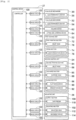
- Custom section forming device 12 is a so-called 3D printer, and includes conveyance device 20, first shaping unit 22, second shaping unit 24, mounting unit 26, and control device (refer to Fig. 2 ) 27. Conveyance device 20, first shaping unit 22, second shaping unit 24, and mounting unit 26 are arranged on base 28 of custom section forming device 12.
- Base 28 has a substantially rectangular shape, and in the following description, the longitudinal direction of base 28 will be referred to as the X-axis direction, the lateral direction of base 28 will be referred to as the Y-axis direction, and the direction orthogonal to both the X-axis direction and the Y-axis direction will be referred to as the Z-axis direction.
- Conveyance device 20 includes X-axis slide mechanism 30 and Y-axis slide mechanism 32.
- X-axis slide mechanism 30 includes X-axis slide rail 34 and X-axis slider 36.
- X-axis slide rail 34 is disposed on base 28 so as to extend in the X-axis direction.
- X-axis slider 36 is held by X-axis slide rail 34 so as to be slidable in the X-axis direction.
- X-axis slide mechanism 30 includes electromagnetic motor (refer to Fig. 2 ) 38, and by driving electromagnetic motor 38, X-axis slider 36 moves to any position in the X-axis direction.
- Y-axis slide mechanism 32 includes Y-axis slide rail 50 and stage 52.
- Y-axis slide rail 50 is disposed on base 28 so as to extend in the Y-axis direction and is movable in the X-axis direction.
- One end of Y-axis slide rail 50 is coupled to X-axis slider 36.
- stage 52 is held so as to be slidable in the Y-axis direction.
- Y-axis slide mechanism 32 includes electromagnetic motor (refer to Fig. 2 ) 56, and by driving electromagnetic motor 56, stage 52 moves to any position in the Y-axis direction.
- stage 52 is moved to any position on base 28
- Stage 52 includes base plate 60, holding device 62, and lifting and lowering device 64.
- Base plate 60 is formed on a flat plate shape, and the printed substrate is placed on the upper surface.
- Holding devices 62 are provided on both sides of base plate 60 in the X-axis direction. Both edges of the printed substrate in the X-axis direction placed on base plate 60 are pinched by holding device 62, the printed substrate is fixedly held.
- lifting and lowering device 64 is disposed below base plate 60, and lifts and lowers base plate 60.
- First shaping unit 22 is a unit for shaping a wiring on the printed substrate placed on base plate 60 of stage 52, and includes first printing section 72 and firing section 74.
- First printing section 72 includes inkjet head (refer to Fig. 2 ) 76, and inkjet head 76 discharges metal ink in a line shape.
- the metal ink is ink in which fine metal particles are dispersed in a solvent.
- Inkjet head 76 discharges the metal ink from multiple nozzles by a piezo type using a piezoelectric element, for example.
- Firing section 74 includes laser irradiation device (refer to Fig. 2 ) 78.
- Laser irradiation device 78 is a device for causing the discharged metal ink to be irradiated with laser, and the metal ink irradiated with the laser is fired to form the wiring.
- Firing of the metal ink is a phenomenon in which conductivity is increased by vaporizing solvent or decomposing a metal fine particle protective film by applying energy and contacting or fusing the metal fine particles. Then, by the metal ink being fired, the metal wiring is formed.
- the ink firing may be performed by a collective heating method at a temperature at which necessary energy can be applied without using a laser.
- second shaping unit 24 is a unit for shaping a resin layer on the printed substrate placed on base plate 60 of stage 52, and includes second printing section 84, discharge section 85, and curing section 86.
- the second printing section 84 includes inkjet head (refer to Fig. 2 ) 88, and inkjet head 88 discharges UV curable resin.
- the UV curable resin is resin that is cured by being irradiated with the ultraviolet rays.
- the inkjet head 88 may be, for example, a piezo type using the piezoelectric element, or may be a thermal type in which the resin is heated to generate bubbles which is discharged from multiple nozzles.
- Discharge section 85 includes dispense head (refer to Fig. 2 ) 89, and dispense head 89 discharges the conductive UV curable resin.
- the conductive UV curable resin is the resin on which the metal fine particles are dispersed on the resin cured by being irradiated with the ultraviolet rays. Then, the resin is cured and shrinks by being irradiated with the ultraviolet rays, the metal fine particles are brought into close contact with each other, and the conductive UV curable resin exhibits the conductivity.
- Dispense head 89 discharges the conductive UV curable resin from one nozzle having a diameter larger than the diameter of the nozzle of inkjet head 76.
- Dispense head 89 may be, for example, a transfer head that performs a paste-transfer with a stamp, and the conductive UV curable resin may be, for example, conductive thermosetting resin.
- Curing section 86 includes flattening device (refer to Fig. 2 ) 90 and irradiation device (refer to Fig. 2 ) 92.
- Flattening device 90 is for flattening the upper surface of the UV curable resin discharged by inkjet head 88, and for example, by scraping off the excess resin with a roller or a blade while leveling the top surface of the UV curable resin, a thickness of the UV curable resin is uniformed.
- irradiation device 92 includes a mercury lamp or an LED as a light source, and causes the discharged UV curable resin or the conductive UV curable resin to be irradiated with the ultraviolet rays. In this way, the discharged UV curable resin is cured to form the resin layer, and the conductive UV curable resin is cured to form the wiring.
- Mounting unit 26 is a unit for mounting the electronic components on the printed substrate placed on base plate 60 of stage 52, and includes supply section 100 and mounting section 102.
- Supply section 100 includes multiple tape feeders (refer to Fig. 2 ) 110 for feeding the taped electronic components one by one, and supplies the electronic components to the supply position.
- supply section 100 may be a tray-type supply device that picks up and supplies the electronic components from the tray.
- supply section 100 may be configured to include both the tape type and the tray type, or other type of supply device.
- Mounting section 102 includes mounting head (refer to Fig. 2 ) 112 and movement device (refer to Fig. 2 ) 114.
- Mounting head 112 includes a suction nozzle (not illustrated) for picking up and holding the electronic component.
- the suction nozzle is supplied with a negative pressure from a positive and negative pressure supply device (not illustrated), and then, picks up and holds the electronic component by suction of air. Then, by a slight positive pressure being supplied from the positive and negative pressure supply device, the electronic component is separated.
- movement device 114 moves mounting head 112 between the supply position of the electronic component by tape feeder 110 and the printed substrate placed on base plate 60. As a result, in mounting section 102, the electronic component supplied from tape feeder 110 is held by the suction nozzle, and the electronic component held by the suction nozzle is mounted on the printed substrate.
- control device 27 includes controller 120 and multiple drive circuits 122.
- Multiple drive circuits 122 are respectively connected to electromagnetic motors 38 and 56, holding device 62, lifting and lowering device 64, inkjet head 76, laser irradiation device 78, inkjet head 88, dispense head 89, flattening device 90, irradiation device 92, tape feeder 110, mounting head 112, and movement device 114.
- Controller 120 includes a CPU, a ROM, a RAM, and the like and is mainly a computer, and is connected to multiple drive circuits 122. As a result, the operations of conveyance device 20, first shaping unit 22, second shaping unit 24, and mounting unit 26 are controlled by controller 120.
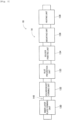
- general-purpose section forming device 14 is a general printed substrate manufacturing device, and includes inner layer plate forming unit 130, solder resist forming unit 132, rust prevention unit 133, solder printing unit 134, mounting unit 136, heating unit 138, and conveyor device 140 as illustrated in Fig. 3 .
- Inner layer plate forming unit 130 is a unit that forms inner layer plate (refer to Fig. 4 ) 150, and forms inner layer plate 150 using a pressure-boding device (not illustrated), a photosensitive device (not illustrated), a surface treatment device (not illustrated), and the like.
- a copper foil is pressure-bonded to insulating layer (refer to Fig. 4 ) 152 such as an interlayer material or a prepreg by the pressure-boding device.
- insulating layer (refer to Fig. 4 ) 152 such as an interlayer material or a prepreg by the pressure-boding device.
- an unevenness is formed on the pressure-bonded surface of the copper foil, an unevenness is formed on the pressure-bonded surface of insulating layer 152.
- inner layer plate 150 configured to include insulating layer 152 and copper pattern (refer to Fig. 4 ) 154 is formed.
- unevenness is formed on a top surface of insulating layer 152 by a surface treatment device.
- a method of forming the unevenness on the top surface of insulating layer 152 there is a method in which the surface of insulating layer 152 is chemically roughened with potassium permanganate or the like to form the unevenness, or a method in which the top surface of insulating layer 152 is physically roughened by blasting or the like to form the unevenness. Then, by an electroless plating process, a copper thin film is formed on the surface of insulating layer 152 on which the unevenness is formed.
- a plating resist is formed on the top surface of the copper thin film along the wiring pattern, and then, electrolytic plating process is performed. As a result, the copper plating is deposited on the places where the plating resist is not formed. Then, by removing the plating resist and etching the copper thin film, inner layer plate 150 composed of insulating layer 152 and copper pattern 154 is formed.
- solder resist forming unit 132 is a unit that forms solder resist (refer to Fig. 5 ) 160 on the top surface of inner layer plate 150, and forms solder resist 160 by a printing device (not illustrated), the irradiation device (not illustrated), or the like. Specifically, an exposure mask (not illustrated) is brought into close contact with the top surface of inner layer plate 150, and the UV curable resin is printed on the exposure mask by the printing device. A through-hole is formed on the exposure mask so that a portion of copper pattern 154 other than pad (refer to Fig.
- the UV curable resin is irradiated with ultraviolet rays by the irradiation device through the exposure mask so that the UV curable resin is cured, and in the subsequent development step, the unexposed solder resist on pad 162 is dissolved, so that solder resist 160 is formed on the top surface of inner layer plate 150 in a state where pad 162 exposed.
- the mask design of the exposed part and the unexposed part is negative-positive reversed.
- rust prevention unit 133 is a unit for preventing the rust on pad 162 of copper pattern 154, and prevent the rust on pad 162 with a palladium removing device (not illustrated), a plating device (not illustrated), or the like. Specifically, first, a palladium removing process is performed on the top surface of inner layer plate 150 on which solder resist 160 is formed. This is because the metal catalyst used in the pre-process remains on the top surface of inner layer plate 150. Then, after the palladium removing process, inner layer plate 150 having solder resist 160 formed thereon is subjected to the electroless nickel-gold plating process in the plating device. As a result, pad 162 is covered with nickel-gold plating (refer to Fig. 6 ) 166.
- solder printing unit 134 is a unit that prints solder on the opening of solder resist 160, that is, pad 162 exposed from solder resist 160, and the solder is printed on pad 162 by the printing device (not illustrated).
- a solder mask (not illustrated) is brought into close contact with the top surface of solder resist 160, and the solder paste is printed on the solder mask by a printing device.
- the through-hole is formed on the solder mask so that pad 162 of copper pattern 154 is exposed, and solder paste (refer to Fig. 7 ) 168 is printed on the upper surface of pad 162 covered with nickel-gold plating 166.
- Mounting unit 136 is a unit for mounting electronic components (refer to Fig. 13 ) 170 on the upper surface of solder resist 160, and mounts electronic components 170 using a tape feeder (not illustrated), a mounting head (not illustrated), and a movement device (not illustrated).
- the tape feeder, the mounting head, and the movement device included in mounting unit 136 are the same as tape feeder 110, mounting head 112, and movement device 114 included in mounting unit 26 of custom section forming device 12. Therefore, in mounting unit 136, electronic component 170 supplied from the tape feeder is held by the suction nozzle, and electronic component 170 held by the suction nozzle is mounted on the upper surface of solder resist 160. At this time, electronic component 170 is mounted on the upper surface of solder resist 160 so that electrode 172 of electronic component 170 comes in contact with solder paste 168 discharged on the upper surface of pad 162.
- Heating unit 138 is a unit for heating solder paste 168, and solder paste 168 is heated by a reflow furnace or the like. As a result, electronic component 170 is fixedly mounted on the upper surface of solder resist 160 in a state of being electrically connected to copper pattern 154 of inner layer plate 150.
- Conveyor device 140 is a device that conveys the printed substrate in an order of inner layer plate forming unit 130, solder resist forming unit 132, rust prevention unit 133, solder printing unit 134, mounting unit 136, and heating unit 138. As a result, the printed substrate is manufactured by the work in each unit.
- circuit forming system 10 by the above-described configuration, in a predetermined region (hereinafter, referred to as a "general-purpose region"), a printed substrate forming step is performed by general-purpose section forming device 14. In addition, in a region different from the general-purpose region (hereinafter referred to as a "custom region”), the printed substrate forming step is performed by custom section forming device 12.
- inner layer plate 150 illustrated in Fig. 4 is formed in inner layer plate forming unit 130 of general-purpose section forming device 14.
- inner layer plate 150 illustrated in Fig. 4 is formed.
- formed onner layer plate 150 is conveyed into solder resist forming unit 132 by conveyor device 140.
- solder resist forming unit 132 as illustrated in Fig. 5 , solder resist 160 is formed only on general-purpose region 180 of inner layer plate 150.
- the through-hole is not formed on the portion covering custom region 182, and the resin for the solder resist is not exposed in custom region 182.
- the mask design of the exposed part and the unexposed part is negative-positive reversed.
- solder resist 160 is formed, inner layer plate 150 is conveyed into rust prevention unit 133 by conveyor device 140. Then, in rust prevention unit 133, the nickel-gold plating process is performed after the palladium removing process is performed. As a result, as illustrated in Fig. 6 , in general-purpose region 180, pad 162 exposed from solder resist 160 is covered with nickel-gold plating 166. In addition, in custom region 182 also, pad 162 exposed from insulating layer 152 is covered with nickel-gold plating 166.
- solder printing unit 134 solder paste 168 is printed on the opening of solder resist 160 formed on general-purpose region 180, that is, the upper surface of pad 162 exposed from solder resist 160.
- solder mask used for printing the solder paste the through-hole is not formed on the portion covering custom region 182, and solder paste 168 is not printed in custom region 182.
- inner layer plate 150 on which solder paste 168 is printed is taken out from general-purpose section forming device 14.
- inner layer plate 150 is set on base plate 60 of stage 52, and stage 52 is moved below second shaping unit 24.
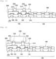
- second shaping unit 24 as illustrated in Fig. 8 , resin layer 200 is formed on the upper surface of inner layer plate 150 in custom region 182.
- the resin layer 200 includes opening 202 for exposing pad 162 of inner layer plate 150, and is formed by repeatedly performing the discharging of the UV curable resin from inkjet head 88 and the discharged UV curable resin being irradiated with the ultraviolet rays emitted by irradiation device 92.
- inkjet head 88 discharges the UV curable resin in a thin film shape on the upper surface of inner layer plate 150 in custom region 182. At this time, inkjet head 88 discharges the UV curable resin so that the upper surface of pad 162 of inner layer plate 150 is exposed. Subsequently, when the UV curable resin is discharged in a thin film shape, in curing section 86, irradiation device 92 causes the thin film shaped UV curable resin to be irradiated with the ultraviolet rays. As a result, thin film 206 is formed on the upper surface of inner layer plate 150.
- inkjet head 88 discharges the UV curable resin only in the upper portion of thin film 206 in a thin film shape. That is, inkjet head 88 discharges the UV curable resin on thin film 206 in a thin film shape so that pad 162 of inner layer plate 150 is exposed. Then, by the UV curable resin discharged in the thin film shape is irradiated with the ultraviolet rays by irradiation device 92, thin film 206 is laminated on thin film 206. In this way, by repeatedly performing the discharging of the UV curable resin on thin film 206 excluding pad 162 and the irradiation with the ultraviolet rays, and the multiple thin films 206 are laminated, resin layer 200 having opening 202 is formed. When the thin films are laminated, the UV curable resin discharged on thin films 206 slightly flows into openings 202. Therefore, an inner wall surface that defines opening 202 is an inclined surface.
- thin film 206 on the upper end surface of resin layer 200 becomes a flat surface by flattening device 90.
- inkjet head 88 discharges the UV curable resin in the thin film shape
- the UV curable resin is flattened by flattening device 90 so that the discharged UV curable resin has a uniform film thickness.
- the flattened UV curable resin is irradiated with ultraviolet rays by irradiation device 92.
- the upper end surface of resin layer 200 becomes a flat surface.
- the UV curable resin is flattened by rollers or the like, however, when the flattened UV curable resin is positioned below the maximum height in general-purpose region 180, the rollers or the like and the upper end part of general-purpose region 180 interfere with each other. Therefore, resin layer 200 is formed such that the upper end surface of resin layer 200 is higher than the maximum height in general-purpose region 180 when resin layer 200 is formed. That is, resin layer 200 is formed such that the upper end surface of resin layer 200 is higher than the upper end surface of solder paste 168 of general-purpose region 180. In this way, a proper operation of the roller can be ensured.
- stage 52 is moved below first shaping unit 22.
- inkjet head 76 discharges the metal ink in a line shape to the inner part of opening 202 of resin layer 200, that is, from pad 162 exposed to opening 202 up to upper surface of opening 202 via the inner wall surface of opening 202.
- laser irradiation device 78 irradiates the metal ink with laser light. At this time, the energy of the laser light is absorbed by the metal ink, and thus, the metal ink generates heat and is fired. As a result, as illustrated in Fig.
- wiring 210 is formed from pad 162 exposed to opening 202 up to the upper surface of opening 202 via the inner wall surface of opening 202.
- the ink fire may be performed by a collective heating method at a temperature at which necessary energy can be applied without using a laser.
- stage 52 is moved below second shaping unit 24.
- resin layer 220 is formed so as to cover the inner part of opening 202 and resin layer 200.
- opening 222 is formed so that a part of wiring 210 formed on the upper surface of resin layer 200 is exposed.
- resin layer 220 is formed by repeatedly performing the discharging of the UV curable resin by inkjet head 88 and the irradiation with the ultraviolet rays by irradiation device 92.
- dispense head 89 discharges conductive UV curable resin 228 to the inner part of opening 222 of resin layer 220, that is, the upper surface of wiring 210 exposed via the opening 222.
- dispense head 89 discharges conductive UV curable resin 228 so that the inner part of opening 222 is filled with conductive UV curable resin 228 and conductive UV curable resin 228 protrudes upward from the opening at the upper end of opening 222.
- conductive UV curable resin 228 being irradiated with the ultraviolet rays by irradiation device 92, conductive UV curable resin 228 exhibits the conductivity.
- a conductive thermosetting resin may be used instead of conductive UV curable resin.
- other printing methods such as a stamp may be used.
- stage 52 is moved to mounting unit 26.
- electronic component (refer to Fig. 12 ) 230 is supplied by tape feeder 110, and mounting head 112 holds electronic component 230.
- mounting head 112 holds electronic component 230.
- electronic component 230 held by mounting head 112 is mounted on the upper surface of resin layer 220.
- electronic component 230 is mounted on the upper surface of resin layer 220 so that electrode 232 of electronic component 230 comes in contact with conductive UV curable resin 228 discharged to opening 222 of resin layer 220.
- electronic component 230 is fixedly mounted on the upper surface of resin layer 220 in a state of being electrically connected to pad 162 of inner layer plate 150, that is, copper pattern 154, via nickel-gold plating 166, wiring 210, and conductive UV curable resin 228.
- inner layer plate 150 on which electronic component 230 is mounted is taken out from the custom section forming device 12. Then, in general-purpose section forming device 14, inner layer plate 150 on which electronic component 230 is mounted is conveyed into mounting unit 136 by conveyance device 20.
- electronic component 170 supplied from tape feeder is held by suction nozzle, and electronic component 170 held by the suction nozzle is mounted on the upper surface of solder resist 160 as illustrated in Fig. 13 .
- electronic component 170 is mounted on the upper surface of solder resist 160 so that electrode 172 of electronic component 170 comes in contact with solder paste 168 discharged on the upper surface of pad 162.
- inner layer plate 150 on which electronic component 170 is mounted on the upper surface of solder resist 160 is conveyed into heating unit 138 by conveyor device 140. Then, heating unit 138 is heated by a reflow furnace. As a result, electronic component 170 is fixedly mounted on the upper surface of solder resist 160 in a state of being electrically connected to copper pattern 154 of inner layer plate 150 via nickel-gold plating 166 and solder paste 168.
- solder resist 160 and the like are formed by general-purpose section forming device 14, and electronic component 170 is mounted on the upper surface of solder resist 160. That is, in general-purpose region 180, the board is formed according to a general method of manufacturing a printer substrate, and in custom region 182, the board is formed according to the method of manufacturing a printer board using the 3D printer. As a result, it is possible to manufacture the printed substrate by taking advantages of each of the method of manufacturing the general printer board and the method of manufacturing the printer board using the 3D printer.
- the printed substrate is manufactured using the exposure mask, or the like, therefore, the printed substrates having the circuit patterns according to the exposure masks or the like can be manufactured in large quantities, and thus, the productivity can be improved, and it is advantageous in terms of cost.
- it is desired to change the manufacturing conditions of only a part of inner layer plate 150 it is needed to create a new exposure mask, and thus, considering the mask creation cost, the mask creation period, and the like, the customizability and on-demand performance are low.
- the circuit pattern can be changed only by changing a program that controls the operation of inkjet head 88 or the like, and it is possible to easily change the manufacturing conditions of only a part of one inner layer plate 150. Therefore, in the method of manufacturing the printed substrate using the 3D printer, the customizability and the on-demand performance are extremely high.
- resin layers 200 and 220 formed of UV curable resin are immature as the materials for the printed substrates from a viewpoint of expansion coefficient, hardness, and the like, and the resistivity and thickness of wiring 210 formed by metal-containing liquid are inferior in resistivity, thickness, or the like of the wiring by the copper plating.
- the productivity is low and the cost required for UV curable resin, metal-containing liquid, and the like is disadvantageous in terms of cost.
- a general-purpose portion of the printed substrate is manufactured by a general method of manufacturing the printed substrate, that is, by general-purpose section forming device 14, and a highly customizable portion of the printed substrate is manufactured by the method of manufacturing the printed substrate using the 3D printer, that is, by custom section forming device 12.
- the power supply section, the control section, the output section, and the like are general-purpose portion and are manufactured by general-purpose section forming device 14.
- a sensing section for detecting a predetermined detection value is manufactured by custom section forming device 12 because the customizability is high differently from that of the wearable devices according to the purpose.
- the manufacturing step is performed on general-purpose region 180 described above, and in a high-customizability portion such as the antenna pattern and the sensing section, the manufacturing step for custom region 182 is performed.
- the manufacturing step for custom region 182 is performed in the general-purpose portion such as the power supply section and the control section.
- circuit forming system 10 when inner layer plate 150 is formed on inner layer plate forming unit 130 of general-purpose section forming device 14, unevennesses are formed on the upper surface of insulating layer 152.
- second shaping unit 24 of custom section forming device 12 resin layer 200 is formed on the upper surface of insulating layer 152 on which the unevennesses are formed. As a result, the adhesion between insulating layer 152 and resin layer 200 is increased, and the strength and reliability of the printed substrate are ensured.
- nickel-gold plating 166 is formed only on pad 162 of inner layer plate 150, and it is possible to prevent nickel-gold plating 166 from being formed on insulating layer 152.
- pad 162 can be appropriately rust-prevented by nickel-gold plating 166, and the conductivity of the conductive section is ensured.
- solder paste 168 is printed on the upper surface of pad 162 using the solder mask, but solder paste 168 may be discharged on the upper surface of pad 162 by a dispenser head or the like. In such a case, not before resin layer 200 is formed on custom region 182 but after resin layer 200 is formed, solder paste 168 may be discharged on the upper surface of pad 162. In addition, if solder paste 168 is discharged on the upper surface of pad 162 after resin layer 200 is formed, the maximum height of general-purpose region 180 when resin layer 200 is formed is the upper surface of solder resist 160. Therefore, resin layer 200 is formed such that the upper end surface of resin layer 200 becomes higher than the upper end surface of solder resist 160 of general-purpose region 180.
- the nickel-gold plating process is performed before resin layer 200 is formed, but the nickel-gold plating process may be performed after resin layer 200 is formed.
- nickel-gold plating 166 is formed only on the upper surface of pad 162 exposed from opening 202 of resin layer 200.
- solder resist 160 is formed only in general-purpose region 180 and not in custom region 182, but solder resist 160 may be formed on both general-purpose region 180 and custom region 182.
- resin layer 250 is formed on the upper surface of solder resist 160.
- opening 252 is formed on resin layer 250 so that the upper surface of nickel-gold plating 166 covering pad 162 is exposed.
- Resin layer 250 is formed by the same method as resin layer 200.
- solder resist 160 in custom region 182 and forming resin layer 250 on the upper surface of solder resist 160, resin layer 250 can be thinned. As a result, it is possible to shorten the formation time of resin layer 250.
- the unevenness is formed on the top surface of solder resist 160 on which resin layer 250 is formed.
- the adhesion between resin layer 250 and solder resist 160 can be improved.
- As a method of forming unevenness on the top surface of solder resist 160 there is a method in which the surface of solder resist 160 is chemically roughened with potassium permanganate or the like to form unevenness, a method in which the surface of solder resist 160 is physically roughened by blasting or the like to form the unevenness.
- the adhesion between resin layer 250 and solder resist 160 can be increased.
- a method for increasing the wettability of the top surface of solder resist 160 there is a method in which plasma treatment is performed on the top surface of solder resist 160.
- the nickel-gold plating process is performed to prevent pad 162 from rust, but rust preventing process other than the nickel-gold plating process can be used.
- nickel-palladium-gold plating process, organic solderability preservative (OSP) process, or the like can be adopted.
- custom section forming device 12 is an example of the printed substrate forming device.
- First shaping unit 22 is an example of a wiring forming device.
- Second shaping unit 24 is an example of the resin layer forming device.
- Inner layer plate 150 is an example of the base.
- Insulating layer 152 is an example of the insulating layer.
- Copper pattern 154 is an example of the conductor layer.
- Solder resist 160 is an example of the solder resist.
- Pad 162 is an example of the conduction section.
- Resin layer 200 is an example of the resin layer. Opening 202 is an example of the opening section.
- Wiring 210 is an example of the wiring.
- the step performed by first shaping unit 22 is an example of the wiring forming step.
- the step performed by second shaping unit 24 is an example of the resin layer forming step.
- the step performed by rust prevention unit 133 is an example of the rust prevention step and the unevenness forming step.
- the step of forming the unevenness on the top surface of solder resist 160 and the step of improving the wettability of the top surface of solder resist 160 are examples of the surface treatment step.
- circuit forming system 10 is configured with two devices, custom section forming device 12 and general-purpose section forming device 14, but may be configured by one device having both the function of custom section forming device 12 and the function of general-purpose section forming device 14.
- custom section forming device printed substrate forming device
- 22 first shaping unit (wiring forming device)
- 24 second shaping unit (resin layer forming device)
- 150 inner layer plate (base)
- 152 insulating layer
- 154 copper pattern (conductor layer)
- 160 solder resist
- 162 pad
- 200 resin layer
- 202 opening (opening section)
- 210 wiring
Landscapes
- Engineering & Computer Science (AREA)
- Microelectronics & Electronic Packaging (AREA)
- Manufacturing & Machinery (AREA)
- Chemical & Material Sciences (AREA)
- Ceramic Engineering (AREA)
- Inorganic Chemistry (AREA)
- Manufacturing Of Printed Wiring (AREA)
- Production Of Multi-Layered Print Wiring Board (AREA)
- Non-Metallic Protective Coatings For Printed Circuits (AREA)
Claims (7)
- Ein Verfahren zur Herstellung eines bedruckten Substrats, umfassend:Bereitstellen einer Basis (150), die aus einer Isolierschicht (152) und einer Leiterschicht (154) besteht, wobei die Basis einen vorbestimmten Bereich (180) umfasst, auf dem ein Lötstopplack mit Durchgangslöchern im Lötstopplack ausgebildet ist, so dass ein Abschnitt der Leiterschicht (154) freiliegt, um Leitungsabschnitte (162) zu bilden, und der mit Lötpaste (168) auf der oberen Fläche dieser Leitungsabschnitte (162) versehen ist;Bedrucken einer ersten Harzschicht (200) mit härtbarem Harz in einem spezifischen Bereich (182), wobei der spezifische Bereich (182) ein anderer Bereich als der vorbestimmte Bereich (180) ist, wobei die erste Harzschicht (200) erste Öffnungen (202) in der Harzschicht (200) zum Freilegen anderer Leitungsabschnitte (162) aufweist;Ausbilden einer Verdrahtung (210) durch Abgeben einer metallhaltigen Flüssigkeit, die feine Metallpartikel enthält, von den durch die ersten Öffnungen (202) freigelegten Leitungsabschnitten (162) auf eine obere Oberfläche der Harzschicht (200) über die Innenwandfläche der ersten Öffnungen (202), und Brennen der metallhaltigen Flüssigkeit;Drucken einer zweiten Harzschicht (220) in dem spezifischen Bereich, um den inneren Teil der ersten Öffnungen (202) und der ersten Harzschicht (200) zu bedecken, wobei die zweite Harzschicht (220) zweite Öffnungen (222) aufweist, so dass ein Teil der Verdrahtung (210) freigelegt ist; undAuftragen eines leitfähigen UV-härtbaren Harzes oder eines leitfähigen wärmehärtbaren Harzes (228) auf den inneren Teil der zweiten Öffnungen (222).
- Verfahren zur Herstellung eines bedruckten Substrats gemäß Anspruch 1, wobeider Harzschichtbildungsschritt ein Schritt des Bildens der Harzschicht (200) mit einem Öffnungsabschnitt (202) und des Freilegens eines Leitungsabschnitts (162) der Leiterschicht (154) über den Öffnungsabschnitt (202) ist, undeinen Rostverhinderungsschritt des Verhinderns von Rost durch Ausführen eines Nickel-Gold-Plattierungsverfahrens, eines Nickel-Palladium-Gold-Plattierungsverfahrens oder eines OSP-Verfahrens an dem freigelegten Leitungsabschnitt (162) umfasst.
- Verfahren zur Herstellung eines bedruckten Substrats gemäß Anspruch 1 oder 2, des Weiteren umfassend:einen Unebenheitsbildungsschritt des Bildens einer Unebenheit auf der oberen Oberfläche der Basis (150) in dem spezifischen Bereich, bevor die Harzschicht (200) gebildet wird, wobeider Harzschichtbildungsschritt ein Schritt des Bildens der Harzschicht (200) auf der oberen Oberfläche der Basis (150) ist, auf der die Unebenheit in dem Unebenheitsbildungsschritt gebildet wird.
- Verfahren zur Herstellung eines bedruckten Substrats gemäß Anspruch 1 oder 2, wobei
der Lötstopplack (160) auch auf dem spezifischen Bereich der Basis (150) gebildet wird, und der Harzschichtbildungsschritt ein Schritt des Bildens der Harzschicht (200) auf der oberen Oberfläche des Lötstopplacks (160) ist, der auf dem spezifischen Bereich gebildet ist. - Verfahren zur Herstellung eines bedruckten Substrats gemäß Anspruch 4, des Weiteren umfassend:einen Oberflächenbehandlungsschritt des Durchführens von mindestens einem von einem Verfahren zum Bilden einer Unebenheit auf der oberen Oberfläche des Lötstopplacks (160), der auf dem spezifischen Bereich gebildet ist, und einem Verfahren zum Erhöhen einer Benetzbarkeit der oberen Oberfläche des Lötstopplacks (160), der auf dem spezifischen Bereich gebildet ist, bevor die Harzschicht (200) gebildet wird, wobeider Harzschichtbildungsschritt ein Schritt zur Bildung der Harzschicht (200) auf der oberen Oberfläche des Lötstopplacks (160) ist, auf der die Behandlung im Oberflächenbehandlungsschritt durchgeführt wird.
- Verfahren zur Herstellung eines bedruckten Substrats gemäß einem der Ansprüche 1 bis 5, wobei
der Harzschichtbildungsschritt ein Schritt des Bildens der Harzschicht (200) ist, so dass eine obere Endfläche der Harzschicht (200) höher ist als eine maximale Höhe in dem vorbestimmten Bereich, wenn die Harzschicht (200) gebildet wird. - Eine Vorrichtung (12) zur Herstellung eines bedruckten Substrats, umfassend:eine Transportvorrichtung (20) für ein bedrucktes Substrat;eine Verdrahtungsbildungsvorrichtung (22), die einen ersten Druckabschnitt (72) zum Abgeben einer metallhaltigen Flüssigkeit, die feine Metallpartikel enthält, und einen Brennabschnitt (74) zum Brennen der metallhaltigen Flüssigkeit umfasst;eine Harzschichtbildungsvorrichtung (24) mit einem zweiten Druckabschnitt (84) zum Drucken einer Harzschicht (200) mit härtbarem Harz; undeine Steuerung (120), die die Transportvorrichtung (20), die Verdrahtungsbildungsvorrichtung (22) und die Harzschichtbildungsvorrichtung (24) steuert und die konfiguriert ist, die Schritte nach Anspruch 1 durchzuführen.
Applications Claiming Priority (1)
| Application Number | Priority Date | Filing Date | Title |
|---|---|---|---|
| PCT/JP2018/015318 WO2019198190A1 (ja) | 2018-04-12 | 2018-04-12 | プリント基板形成方法、およびプリント基板形成装置 |
Publications (3)
| Publication Number | Publication Date |
|---|---|
| EP3780916A1 EP3780916A1 (de) | 2021-02-17 |
| EP3780916A4 EP3780916A4 (de) | 2021-04-14 |
| EP3780916B1 true EP3780916B1 (de) | 2025-03-05 |
Family
ID=68164238
Family Applications (1)
| Application Number | Title | Priority Date | Filing Date |
|---|---|---|---|
| EP18914298.7A Active EP3780916B1 (de) | 2018-04-12 | 2018-04-12 | Verfahren zur herstellung eines bedruckten substrats und vorrichtung zur herstellung eines bedruckten substrats |
Country Status (5)
| Country | Link |
|---|---|
| US (1) | US11540397B2 (de) |
| EP (1) | EP3780916B1 (de) |
| JP (1) | JP7075481B2 (de) |
| CN (1) | CN111972052B (de) |
| WO (1) | WO2019198190A1 (de) |
Family Cites Families (26)
| Publication number | Priority date | Publication date | Assignee | Title |
|---|---|---|---|---|
| JPS62252192A (ja) * | 1986-04-24 | 1987-11-02 | 日本電気株式会社 | 印刷配線板の製造方法 |
| JPH066530Y2 (ja) * | 1988-09-30 | 1994-02-16 | 株式会社富士通ゼネラル | プリント配線板 |
| US5872051A (en) * | 1995-08-02 | 1999-02-16 | International Business Machines Corporation | Process for transferring material to semiconductor chip conductive pads using a transfer substrate |
| JPH11163499A (ja) * | 1997-11-28 | 1999-06-18 | Nitto Boseki Co Ltd | プリント配線板の製造方法及びこの製造方法によるプリント配線板 |
| JPH11168171A (ja) * | 1997-12-03 | 1999-06-22 | Denso Corp | 混成集積回路装置及びその製造方法 |
| KR100855529B1 (ko) * | 1998-09-03 | 2008-09-01 | 이비덴 가부시키가이샤 | 다층프린트배선판 및 그 제조방법 |
| TW552832B (en) * | 2001-06-07 | 2003-09-11 | Lg Electronics Inc | Hole plugging method for printed circuit boards, and hole plugging device |
| JP4089198B2 (ja) * | 2001-10-05 | 2008-05-28 | 凸版印刷株式会社 | 半導体装置用基板の製造方法 |
| DE60326760D1 (de) * | 2002-09-18 | 2009-04-30 | Ebara Corp | Verfahren zum verbinden |
| JP2005005585A (ja) * | 2003-06-13 | 2005-01-06 | Shindo Denshi Kogyo Kk | フレキシブルプリント回路基板、フレキシブルプリント回路基板モジュール、およびフレキシブルプリント回路基板の製造方法 |
| JP2004006927A (ja) * | 2003-06-30 | 2004-01-08 | Ngk Spark Plug Co Ltd | 半田バンプを有する配線基板及び該配線基板の製造方法並びに半田バンプ形成用メタルマスク |
| JP2006059942A (ja) | 2004-08-19 | 2006-03-02 | Mamoru Onda | 配線基板の製法およびそれを用いて製造した配線基板ならびに電子装置、電子機器 |
| KR100797694B1 (ko) * | 2006-06-13 | 2008-01-23 | 삼성전기주식회사 | 솔더볼 접착강도가 우수한 인쇄회로기판 및 그 제조방법 |
| CN101529585B (zh) * | 2006-10-20 | 2012-07-04 | 日本电气株式会社 | 电子设备的封装结构及封装制造方法 |
| EP2440024B1 (de) * | 2009-06-01 | 2014-03-12 | Sumitomo Electric Industries, Ltd. | Verbindungsverfahren |
| JP2011054620A (ja) * | 2009-08-31 | 2011-03-17 | Murata Mfg Co Ltd | 多層配線基板の製造方法 |
| US20110048775A1 (en) * | 2009-08-31 | 2011-03-03 | Ibiden Co., Ltd. | Printed wiring board and method for manufacturing the same |
| KR101608745B1 (ko) * | 2009-12-30 | 2016-04-05 | 삼성전자 주식회사 | 인쇄회로기판조립체의 제조방법 |
| JP2012009510A (ja) * | 2010-06-22 | 2012-01-12 | Sumitomo Bakelite Co Ltd | 金属微細パターン付き基材、プリント配線板、及び半導体装置、並びに、金属微細パターン付き基材及びプリント配線板の製造方法 |
| US8866300B1 (en) * | 2011-06-05 | 2014-10-21 | Nuvotronics, Llc | Devices and methods for solder flow control in three-dimensional microstructures |
| WO2013046442A1 (ja) * | 2011-09-30 | 2013-04-04 | 株式会社メイコー | 基板及びその製造方法 |
| JP2015072984A (ja) * | 2013-10-02 | 2015-04-16 | イビデン株式会社 | プリント配線板、プリント配線板の製造方法、パッケージ−オン−パッケージ |
| JP2016021534A (ja) * | 2014-07-15 | 2016-02-04 | イビデン株式会社 | プリント配線板およびその製造方法 |
| WO2016125275A1 (ja) * | 2015-02-05 | 2016-08-11 | 富士機械製造株式会社 | データ変換装置及び積層造形システム |
| US9961767B2 (en) * | 2015-02-10 | 2018-05-01 | Shinko Electric Industires Co., Ltd. | Circuit board and method of manufacturing circuit board |
| JP2016197624A (ja) * | 2015-04-02 | 2016-11-24 | イビデン株式会社 | インダクタ部品、インダクタ部品の製造方法、インダクタ部品を内蔵するプリント配線板 |
-
2018
- 2018-04-12 EP EP18914298.7A patent/EP3780916B1/de active Active
- 2018-04-12 WO PCT/JP2018/015318 patent/WO2019198190A1/ja not_active Ceased
- 2018-04-12 US US16/981,079 patent/US11540397B2/en active Active
- 2018-04-12 JP JP2020513006A patent/JP7075481B2/ja active Active
- 2018-04-12 CN CN201880091669.2A patent/CN111972052B/zh active Active
Also Published As
| Publication number | Publication date |
|---|---|
| CN111972052B (zh) | 2024-02-06 |
| US20210029832A1 (en) | 2021-01-28 |
| JP7075481B2 (ja) | 2022-05-25 |
| JPWO2019198190A1 (ja) | 2020-10-22 |
| CN111972052A (zh) | 2020-11-20 |
| WO2019198190A1 (ja) | 2019-10-17 |
| US11540397B2 (en) | 2022-12-27 |
| EP3780916A1 (de) | 2021-02-17 |
| EP3780916A4 (de) | 2021-04-14 |
Similar Documents
| Publication | Publication Date | Title |
|---|---|---|
| US11849545B2 (en) | Circuit formation method | |
| CN109314086B (zh) | 电路形成方法 | |
| JP6714109B2 (ja) | 回路形成方法、および回路形成装置 | |
| JP6987975B2 (ja) | 3次元構造物形成方法、および3次元構造物形成装置 | |
| JP7053832B2 (ja) | 回路形成方法、および回路形成装置 | |
| US11570900B2 (en) | Circuit forming method | |
| US11540397B2 (en) | Printed substrate forming method | |
| WO2021214813A1 (ja) | 回路形成方法、および回路形成装置 | |
| JP7411452B2 (ja) | 回路形成方法 | |
| US20250142734A1 (en) | Electrical circuit formation method, and electrical circuit formation device | |
| JP7826344B2 (ja) | 電気回路形成方法、および電気回路形成装置 | |
| WO2024062605A1 (ja) | 回路形成装置、および回路形成方法 | |
| JP7282906B2 (ja) | 部品装着方法、および部品装着装置 | |
| JP7325532B2 (ja) | 積層造形法による3次元造形物の製造方法及び3次元造形物製造装置 | |
| WO2021166139A1 (ja) | 回路形成方法 | |
| JP7811218B2 (ja) | 回路形成方法、および回路形成装置 | |
| WO2026033712A1 (ja) | 回路形成方法、および回路形成装置 | |
| WO2019171531A1 (ja) | 情報処理装置 | |
| JPWO2019186780A1 (ja) | 回路形成方法、および回路形成装置 | |
| WO2022101965A1 (ja) | 回路形成方法 | |
| WO2025220064A1 (ja) | 回路形成方法、および回路形成装置 | |
| JP2024168901A (ja) | 回路基板形成装置、および回路基板形成方法 | |
| JP2023166848A (ja) | 電気回路形成方法、および電気回路形成装置 | |
| CN121128323A (zh) | 电路形成方法及电路形成装置 | |
| WO2022201231A1 (ja) | 判定装置、造形方法、および造形装置 |
Legal Events
| Date | Code | Title | Description |
|---|---|---|---|
| STAA | Information on the status of an ep patent application or granted ep patent |
Free format text: STATUS: THE INTERNATIONAL PUBLICATION HAS BEEN MADE |
|
| PUAI | Public reference made under article 153(3) epc to a published international application that has entered the european phase |
Free format text: ORIGINAL CODE: 0009012 |
|
| STAA | Information on the status of an ep patent application or granted ep patent |
Free format text: STATUS: REQUEST FOR EXAMINATION WAS MADE |
|
| 17P | Request for examination filed |
Effective date: 20200821 |
|
| AK | Designated contracting states |
Kind code of ref document: A1 Designated state(s): AL AT BE BG CH CY CZ DE DK EE ES FI FR GB GR HR HU IE IS IT LI LT LU LV MC MK MT NL NO PL PT RO RS SE SI SK SM TR |
|
| AX | Request for extension of the european patent |
Extension state: BA ME |
|
| A4 | Supplementary search report drawn up and despatched |
Effective date: 20210315 |
|
| RIC1 | Information provided on ipc code assigned before grant |
Ipc: H05K 3/00 20060101AFI20210309BHEP Ipc: H05K 3/10 20060101ALI20210309BHEP Ipc: H05K 3/32 20060101ALI20210309BHEP Ipc: H05K 3/34 20060101ALI20210309BHEP Ipc: H05K 1/11 20060101ALI20210309BHEP Ipc: H05K 1/18 20060101ALI20210309BHEP |
|
| DAV | Request for validation of the european patent (deleted) | ||
| DAX | Request for extension of the european patent (deleted) | ||
| P01 | Opt-out of the competence of the unified patent court (upc) registered |
Effective date: 20230328 |
|
| STAA | Information on the status of an ep patent application or granted ep patent |
Free format text: STATUS: EXAMINATION IS IN PROGRESS |
|
| 17Q | First examination report despatched |
Effective date: 20231113 |
|
| GRAP | Despatch of communication of intention to grant a patent |
Free format text: ORIGINAL CODE: EPIDOSNIGR1 |
|
| STAA | Information on the status of an ep patent application or granted ep patent |
Free format text: STATUS: GRANT OF PATENT IS INTENDED |
|
| INTG | Intention to grant announced |
Effective date: 20241016 |
|
| GRAS | Grant fee paid |
Free format text: ORIGINAL CODE: EPIDOSNIGR3 |
|
| GRAA | (expected) grant |
Free format text: ORIGINAL CODE: 0009210 |
|
| STAA | Information on the status of an ep patent application or granted ep patent |
Free format text: STATUS: THE PATENT HAS BEEN GRANTED |
|
| AK | Designated contracting states |
Kind code of ref document: B1 Designated state(s): AL AT BE BG CH CY CZ DE DK EE ES FI FR GB GR HR HU IE IS IT LI LT LU LV MC MK MT NL NO PL PT RO RS SE SI SK SM TR |
|
| REG | Reference to a national code |
Ref country code: GB Ref legal event code: FG4D |
|
| REG | Reference to a national code |
Ref country code: CH Ref legal event code: EP |
|
| REG | Reference to a national code |
Ref country code: IE Ref legal event code: FG4D |
|
| REG | Reference to a national code |
Ref country code: DE Ref legal event code: R096 Ref document number: 602018079948 Country of ref document: DE |
|
| PG25 | Lapsed in a contracting state [announced via postgrant information from national office to epo] |
Ref country code: RS Free format text: LAPSE BECAUSE OF FAILURE TO SUBMIT A TRANSLATION OF THE DESCRIPTION OR TO PAY THE FEE WITHIN THE PRESCRIBED TIME-LIMIT Effective date: 20250605 |
|
| PG25 | Lapsed in a contracting state [announced via postgrant information from national office to epo] |
Ref country code: FI Free format text: LAPSE BECAUSE OF FAILURE TO SUBMIT A TRANSLATION OF THE DESCRIPTION OR TO PAY THE FEE WITHIN THE PRESCRIBED TIME-LIMIT Effective date: 20250305 |
|
| REG | Reference to a national code |
Ref country code: NL Ref legal event code: MP Effective date: 20250305 |
|
| PG25 | Lapsed in a contracting state [announced via postgrant information from national office to epo] |
Ref country code: ES Free format text: LAPSE BECAUSE OF FAILURE TO SUBMIT A TRANSLATION OF THE DESCRIPTION OR TO PAY THE FEE WITHIN THE PRESCRIBED TIME-LIMIT Effective date: 20250305 |
|
| REG | Reference to a national code |
Ref country code: LT Ref legal event code: MG9D |
|
| PG25 | Lapsed in a contracting state [announced via postgrant information from national office to epo] |
Ref country code: NO Free format text: LAPSE BECAUSE OF FAILURE TO SUBMIT A TRANSLATION OF THE DESCRIPTION OR TO PAY THE FEE WITHIN THE PRESCRIBED TIME-LIMIT Effective date: 20250605 |
|
| PG25 | Lapsed in a contracting state [announced via postgrant information from national office to epo] |
Ref country code: HR Free format text: LAPSE BECAUSE OF FAILURE TO SUBMIT A TRANSLATION OF THE DESCRIPTION OR TO PAY THE FEE WITHIN THE PRESCRIBED TIME-LIMIT Effective date: 20250305 |
|
| PG25 | Lapsed in a contracting state [announced via postgrant information from national office to epo] |
Ref country code: LV Free format text: LAPSE BECAUSE OF FAILURE TO SUBMIT A TRANSLATION OF THE DESCRIPTION OR TO PAY THE FEE WITHIN THE PRESCRIBED TIME-LIMIT Effective date: 20250305 |
|
| PG25 | Lapsed in a contracting state [announced via postgrant information from national office to epo] |
Ref country code: GR Free format text: LAPSE BECAUSE OF FAILURE TO SUBMIT A TRANSLATION OF THE DESCRIPTION OR TO PAY THE FEE WITHIN THE PRESCRIBED TIME-LIMIT Effective date: 20250606 Ref country code: BG Free format text: LAPSE BECAUSE OF FAILURE TO SUBMIT A TRANSLATION OF THE DESCRIPTION OR TO PAY THE FEE WITHIN THE PRESCRIBED TIME-LIMIT Effective date: 20250305 |
|
| REG | Reference to a national code |
Ref country code: AT Ref legal event code: MK05 Ref document number: 1774174 Country of ref document: AT Kind code of ref document: T Effective date: 20250305 |
|
| PG25 | Lapsed in a contracting state [announced via postgrant information from national office to epo] |
Ref country code: NL Free format text: LAPSE BECAUSE OF FAILURE TO SUBMIT A TRANSLATION OF THE DESCRIPTION OR TO PAY THE FEE WITHIN THE PRESCRIBED TIME-LIMIT Effective date: 20250305 |
|
| PG25 | Lapsed in a contracting state [announced via postgrant information from national office to epo] |
Ref country code: SE Free format text: LAPSE BECAUSE OF FAILURE TO SUBMIT A TRANSLATION OF THE DESCRIPTION OR TO PAY THE FEE WITHIN THE PRESCRIBED TIME-LIMIT Effective date: 20250305 |
|
| PG25 | Lapsed in a contracting state [announced via postgrant information from national office to epo] |
Ref country code: SM Free format text: LAPSE BECAUSE OF FAILURE TO SUBMIT A TRANSLATION OF THE DESCRIPTION OR TO PAY THE FEE WITHIN THE PRESCRIBED TIME-LIMIT Effective date: 20250305 |
|
| PG25 | Lapsed in a contracting state [announced via postgrant information from national office to epo] |
Ref country code: PT Free format text: LAPSE BECAUSE OF FAILURE TO SUBMIT A TRANSLATION OF THE DESCRIPTION OR TO PAY THE FEE WITHIN THE PRESCRIBED TIME-LIMIT Effective date: 20250707 |
|
| PG25 | Lapsed in a contracting state [announced via postgrant information from national office to epo] |
Ref country code: PL Free format text: LAPSE BECAUSE OF FAILURE TO SUBMIT A TRANSLATION OF THE DESCRIPTION OR TO PAY THE FEE WITHIN THE PRESCRIBED TIME-LIMIT Effective date: 20250305 Ref country code: IT Free format text: LAPSE BECAUSE OF FAILURE TO SUBMIT A TRANSLATION OF THE DESCRIPTION OR TO PAY THE FEE WITHIN THE PRESCRIBED TIME-LIMIT Effective date: 20250305 |
|
| PG25 | Lapsed in a contracting state [announced via postgrant information from national office to epo] |
Ref country code: AT Free format text: LAPSE BECAUSE OF FAILURE TO SUBMIT A TRANSLATION OF THE DESCRIPTION OR TO PAY THE FEE WITHIN THE PRESCRIBED TIME-LIMIT Effective date: 20250305 |
|
| PG25 | Lapsed in a contracting state [announced via postgrant information from national office to epo] |
Ref country code: EE Free format text: LAPSE BECAUSE OF FAILURE TO SUBMIT A TRANSLATION OF THE DESCRIPTION OR TO PAY THE FEE WITHIN THE PRESCRIBED TIME-LIMIT Effective date: 20250305 Ref country code: CZ Free format text: LAPSE BECAUSE OF FAILURE TO SUBMIT A TRANSLATION OF THE DESCRIPTION OR TO PAY THE FEE WITHIN THE PRESCRIBED TIME-LIMIT Effective date: 20250305 |
|
| PG25 | Lapsed in a contracting state [announced via postgrant information from national office to epo] |
Ref country code: RO Free format text: LAPSE BECAUSE OF FAILURE TO SUBMIT A TRANSLATION OF THE DESCRIPTION OR TO PAY THE FEE WITHIN THE PRESCRIBED TIME-LIMIT Effective date: 20250305 |
|
| PG25 | Lapsed in a contracting state [announced via postgrant information from national office to epo] |
Ref country code: SK Free format text: LAPSE BECAUSE OF FAILURE TO SUBMIT A TRANSLATION OF THE DESCRIPTION OR TO PAY THE FEE WITHIN THE PRESCRIBED TIME-LIMIT Effective date: 20250305 |
|
| PG25 | Lapsed in a contracting state [announced via postgrant information from national office to epo] |
Ref country code: IS Free format text: LAPSE BECAUSE OF FAILURE TO SUBMIT A TRANSLATION OF THE DESCRIPTION OR TO PAY THE FEE WITHIN THE PRESCRIBED TIME-LIMIT Effective date: 20250705 |
|
| REG | Reference to a national code |
Ref country code: CH Ref legal event code: H13 Free format text: ST27 STATUS EVENT CODE: U-0-0-H10-H13 (AS PROVIDED BY THE NATIONAL OFFICE) Effective date: 20251125 |
|
| REG | Reference to a national code |
Ref country code: DE Ref legal event code: R097 Ref document number: 602018079948 Country of ref document: DE |
|
| PG25 | Lapsed in a contracting state [announced via postgrant information from national office to epo] |
Ref country code: LU Free format text: LAPSE BECAUSE OF NON-PAYMENT OF DUE FEES Effective date: 20250412 |
|
| PG25 | Lapsed in a contracting state [announced via postgrant information from national office to epo] |
Ref country code: MC Free format text: LAPSE BECAUSE OF FAILURE TO SUBMIT A TRANSLATION OF THE DESCRIPTION OR TO PAY THE FEE WITHIN THE PRESCRIBED TIME-LIMIT Effective date: 20250305 |
|
| REG | Reference to a national code |
Ref country code: BE Ref legal event code: MM Effective date: 20250430 |
|
| PLBE | No opposition filed within time limit |
Free format text: ORIGINAL CODE: 0009261 |
|
| STAA | Information on the status of an ep patent application or granted ep patent |
Free format text: STATUS: NO OPPOSITION FILED WITHIN TIME LIMIT |
|
| PG25 | Lapsed in a contracting state [announced via postgrant information from national office to epo] |
Ref country code: DK Free format text: LAPSE BECAUSE OF FAILURE TO SUBMIT A TRANSLATION OF THE DESCRIPTION OR TO PAY THE FEE WITHIN THE PRESCRIBED TIME-LIMIT Effective date: 20250305 |
|
| REG | Reference to a national code |
Ref country code: CH Ref legal event code: L10 Free format text: ST27 STATUS EVENT CODE: U-0-0-L10-L00 (AS PROVIDED BY THE NATIONAL OFFICE) Effective date: 20260114 |
|
| PG25 | Lapsed in a contracting state [announced via postgrant information from national office to epo] |
Ref country code: BE Free format text: LAPSE BECAUSE OF NON-PAYMENT OF DUE FEES Effective date: 20250430 |
|
| PG25 | Lapsed in a contracting state [announced via postgrant information from national office to epo] |
Ref country code: CH Free format text: LAPSE BECAUSE OF NON-PAYMENT OF DUE FEES Effective date: 20250430 |
|
| 26N | No opposition filed |
Effective date: 20251208 |
|
| GBPC | Gb: european patent ceased through non-payment of renewal fee |
Effective date: 20250605 |
|
| PG25 | Lapsed in a contracting state [announced via postgrant information from national office to epo] |
Ref country code: GB Free format text: LAPSE BECAUSE OF NON-PAYMENT OF DUE FEES Effective date: 20250605 |
|
| PG25 | Lapsed in a contracting state [announced via postgrant information from national office to epo] |
Ref country code: IE Free format text: LAPSE BECAUSE OF NON-PAYMENT OF DUE FEES Effective date: 20250412 |
|
| PGFP | Annual fee paid to national office [announced via postgrant information from national office to epo] |
Ref country code: FR Payment date: 20260309 Year of fee payment: 9 |
|
| PG25 | Lapsed in a contracting state [announced via postgrant information from national office to epo] |
Ref country code: CY Free format text: LAPSE BECAUSE OF FAILURE TO SUBMIT A TRANSLATION OF THE DESCRIPTION OR TO PAY THE FEE WITHIN THE PRESCRIBED TIME-LIMIT Effective date: 20250305 |
|
| PG25 | Lapsed in a contracting state [announced via postgrant information from national office to epo] |
Ref country code: LT Free format text: LAPSE BECAUSE OF FAILURE TO SUBMIT A TRANSLATION OF THE DESCRIPTION OR TO PAY THE FEE WITHIN THE PRESCRIBED TIME-LIMIT Effective date: 20250305 |
|
| PGFP | Annual fee paid to national office [announced via postgrant information from national office to epo] |
Ref country code: DE Payment date: 20260305 Year of fee payment: 9 |