EP3756213B1 - Apparatus with overlapping deep trench and shallow trench and method of fabricating the same with low defect density - Google Patents
Apparatus with overlapping deep trench and shallow trench and method of fabricating the same with low defect density Download PDFInfo
- Publication number
- EP3756213B1 EP3756213B1 EP19757672.1A EP19757672A EP3756213B1 EP 3756213 B1 EP3756213 B1 EP 3756213B1 EP 19757672 A EP19757672 A EP 19757672A EP 3756213 B1 EP3756213 B1 EP 3756213B1
- Authority
- EP
- European Patent Office
- Prior art keywords
- shallow trench
- trench
- dielectric layer
- layer
- forming
- Prior art date
- Legal status (The legal status is an assumption and is not a legal conclusion. Google has not performed a legal analysis and makes no representation as to the accuracy of the status listed.)
- Active
Links
Images


Classifications
-
- H—ELECTRICITY
- H10—SEMICONDUCTOR DEVICES; ELECTRIC SOLID-STATE DEVICES NOT OTHERWISE PROVIDED FOR
- H10W—GENERIC PACKAGES, INTERCONNECTIONS, CONNECTORS OR OTHER CONSTRUCTIONAL DETAILS OF DEVICES COVERED BY CLASS H10
- H10W10/00—Isolation regions in semiconductor bodies between components of integrated devices
- H10W10/10—Isolation regions comprising dielectric materials
- H10W10/17—Isolation regions comprising dielectric materials formed using trench refilling with dielectric materials, e.g. shallow trench isolations
-
- H—ELECTRICITY
- H10—SEMICONDUCTOR DEVICES; ELECTRIC SOLID-STATE DEVICES NOT OTHERWISE PROVIDED FOR
- H10D—INORGANIC ELECTRIC SEMICONDUCTOR DEVICES
- H10D62/00—Semiconductor bodies, or regions thereof, of devices having potential barriers
- H10D62/10—Shapes, relative sizes or dispositions of the regions of the semiconductor bodies; Shapes of the semiconductor bodies
- H10D62/113—Isolations within a component, i.e. internal isolations
- H10D62/115—Dielectric isolations, e.g. air gaps
-
- H—ELECTRICITY
- H10—SEMICONDUCTOR DEVICES; ELECTRIC SOLID-STATE DEVICES NOT OTHERWISE PROVIDED FOR
- H10D—INORGANIC ELECTRIC SEMICONDUCTOR DEVICES
- H10D64/00—Electrodes of devices having potential barriers
- H10D64/111—Field plates
- H10D64/117—Recessed field plates, e.g. trench field plates or buried field plates
-
- H—ELECTRICITY
- H10—SEMICONDUCTOR DEVICES; ELECTRIC SOLID-STATE DEVICES NOT OTHERWISE PROVIDED FOR
- H10P—GENERIC PROCESSES OR APPARATUS FOR THE MANUFACTURE OR TREATMENT OF DEVICES COVERED BY CLASS H10
- H10P14/00—Formation of materials, e.g. in the shape of layers or pillars
- H10P14/60—Formation of materials, e.g. in the shape of layers or pillars of insulating materials
- H10P14/63—Formation of materials, e.g. in the shape of layers or pillars of insulating materials characterised by the formation processes
- H10P14/6326—Deposition processes
- H10P14/6328—Deposition from the gas or vapour phase
- H10P14/6332—Deposition from the gas or vapour phase using thermal evaporation
-
- H—ELECTRICITY
- H10—SEMICONDUCTOR DEVICES; ELECTRIC SOLID-STATE DEVICES NOT OTHERWISE PROVIDED FOR
- H10P—GENERIC PROCESSES OR APPARATUS FOR THE MANUFACTURE OR TREATMENT OF DEVICES COVERED BY CLASS H10
- H10P50/00—Etching of wafers, substrates or parts of devices
- H10P50/69—Etching of wafers, substrates or parts of devices using masks for semiconductor materials
- H10P50/691—Etching of wafers, substrates or parts of devices using masks for semiconductor materials for Group V materials or Group III-V materials
- H10P50/692—Etching of wafers, substrates or parts of devices using masks for semiconductor materials for Group V materials or Group III-V materials characterised by their composition, e.g. multilayer masks or materials
-
- H—ELECTRICITY
- H10—SEMICONDUCTOR DEVICES; ELECTRIC SOLID-STATE DEVICES NOT OTHERWISE PROVIDED FOR
- H10W—GENERIC PACKAGES, INTERCONNECTIONS, CONNECTORS OR OTHER CONSTRUCTIONAL DETAILS OF DEVICES COVERED BY CLASS H10
- H10W10/00—Isolation regions in semiconductor bodies between components of integrated devices
- H10W10/01—Manufacture or treatment
- H10W10/011—Manufacture or treatment of isolation regions comprising dielectric materials
- H10W10/014—Manufacture or treatment of isolation regions comprising dielectric materials using trench refilling with dielectric materials, e.g. shallow trench isolations
- H10W10/0143—Manufacture or treatment of isolation regions comprising dielectric materials using trench refilling with dielectric materials, e.g. shallow trench isolations comprising concurrently refilling multiple trenches having different shapes or dimensions
-
- H—ELECTRICITY
- H10—SEMICONDUCTOR DEVICES; ELECTRIC SOLID-STATE DEVICES NOT OTHERWISE PROVIDED FOR
- H10W—GENERIC PACKAGES, INTERCONNECTIONS, CONNECTORS OR OTHER CONSTRUCTIONAL DETAILS OF DEVICES COVERED BY CLASS H10
- H10W10/00—Isolation regions in semiconductor bodies between components of integrated devices
- H10W10/01—Manufacture or treatment
- H10W10/011—Manufacture or treatment of isolation regions comprising dielectric materials
- H10W10/014—Manufacture or treatment of isolation regions comprising dielectric materials using trench refilling with dielectric materials, e.g. shallow trench isolations
- H10W10/0145—Manufacture or treatment of isolation regions comprising dielectric materials using trench refilling with dielectric materials, e.g. shallow trench isolations of trenches having shapes other than rectangular or V-shape
Definitions
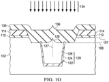
- a polysilicon deposition process 125 is performed to fill the deep trench 122 with a conductive material.
- a DT filler structure 126 is formed in the deep trench 122.
- the DT filler structure 126 may contact the DT oxide liner 124.
- the DT filler structure 126 may directly contact the sidewall of the deep trench 122 where the DT oxide liner 124 is absent.
- a DT filler seam 127 may be formed along a vertical middle section of the FT filler structure 126. The dimensions of the DT filler seam 127 may depend on the aspect ratio of the deep trench 122.
- a chemical mechanical polish process is performed to remove excessive polysilicon material above the deep trench 122. At this point, a conductive deep trench 129 is formed. Then, the remaining nitride cap layer 114 and pad oxide layer 112 are removed and redeposited to complete the deep trench formation sequence and prepare for the shallow trench formation sequence.
- the DT filler seam 127 may trap residuals from the nitride cap layer 114 and the pad oxide layer 112, which may in turn retard the etch rate around the DT filler seam 127. This slower etching may lead to the formation of one or more polysilicon cones 128 near the DT filler seam 127.
- FIG. 1G only shows a single dielectric cone 136 and a single polysilicon cone 128, but in reality, a semiconductor device (e.g., device 100) fabricated under the process steps as shown above may incur many more dielectric cones and silicon cones in a small area. The dielectric cones may be subsequently removed during a chemical mechanical polish process. Nevertheless, the polysilicon cone 128 remains under the dielectric layer 135. As the dielectric layer 135 is mostly transparent, the polysilicon cone 128 is visible or detectable by one or more inspection devices. Thus, the polysilicon cone 128 may obstruct one or more inspection processes for detecting structural defects of the semiconductor device. As a result, yield related issues may remain undetected by the inspection processes. These undetected yield related issues will ultimately impact the yield of a mass production of the semiconductor devices.
- a semiconductor device e.g., device 100
- FIG. 2A shows a flow chart of an example method 200 for fabricating a shallow trench followed by a deep trench free of cone defects.
- the method 200 begins at step 210, which involves forming a shallow trench in a first region of a substrate. Unlike the process as depicted in FIGS. 1A-1G , the method 200 arranges the shallow trench to be formed before the deep trench.
- FIGS. 3A-3I show the partial cross-sectional views of an example semiconductor device 300 during a fabrication process that implements the method 200.
- the semiconductor device 300 is at an early stage of a fabrication process.
- the semiconductor device 300 can be a discrete component device (e.g., a single transistor device) or an integrated circuit having multiple transistor devices.
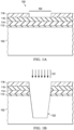
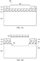
- a pad oxide layer 112, and a nitride cap layer 114 are sequentially formed on a top surface of a semiconductor substrate 102.
- the process parameters for forming the pad oxide layer 112, and the cap nitride layer 114 are essentially the same as described in association with FIG. 1A .
- a photoresist mask 131 is deposited and patterned with an opening exposing a shallow trench (ST) region 106, being a first region of the substrate 102.
- a shallow trench etch process is performed.
- a shallow trench etch process 132 may include a silicon etch to remove the nitride cap layer 114,and the pad oxide layer 112 as exposed by the photoresist mask 131.
- a shallow trench 133 is formed.
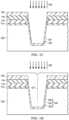
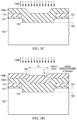
- step 220 involves forming a dielectric layer filling the shallow trench and covering the substrate.
- the dielectric layer has a substantially planar surface positioned over and extending across the shallow trench. The substantially planar surface advantageously allows the photoresist mask for etching a deep trench to be deposited and patterned more accurately. While step 220 can be performed by forming a single dielectric layer that fills the shallow trench (e.g., shallow trench 133), multiple dielectric layers may be formed during step 220 as well.
- FIG. 2B shows a method 220A for forming at least two dielectric layers that fills the shallow trench and covering the substrate.
- the method 220A begins at step 222, which involves forming a shallow trench oxide layer filling the shallow trench.
- the shallow trench oxide layer may be considered as a first oxide layer that fills the shallow trench, and it may be thermally grown onto the etched surface of the shallow trench.
- a first dielectric formation process 134A is performed to formed a first dielectric layer 135A.
- the first dielectric formation process 134A may be a thermal oxidation process or an oxide deposition process (e.g., high density plasma deposition).
- a second dielectric formation process 134B is performed to formed a second dielectric layer 135B.
- the second dielectric formation process 134B may be a thermal oxidation process or an oxide deposition process (e.g., TEOS plasma enhanced chemical vapor deposition).
- the second dielectric layer 135B is a hard mask layer as it serves the function of a hard mask during a subsequent deep trench etching process.
- the second dielectric layer (or hard mask layer) 135B has a substantially planar surface 136.
- the surface of the second dielectric layer (or hard mask layer) 135B is substantially planar when it is sufficiently flat to allow accurate placement and patterning of a photoresist mask for the purpose of etching a deep trench within the shallow trench 133.
- the substantially planar surface 136 may have an aspect ratio defined by a height (H) of the surface over a width (W) that is sufficiently wide to serve as a deep trench aperture.
- the second dielectric layer (or hard mask layer) 135B has a substantially planar surface 136 where the aspect ratio is less than 0.4. In another implementation, for example, the second dielectric layer (or hard mask layer) 135B has a substantially planar surface 136 where the aspect ratio is less than 0.2. In yet another implementation, for example, the second dielectric layer (or hard mask layer) 135B has a substantially planar surface 136 where the aspect ratio is less than 0.1.
- the substantially planar surface 136 can be achieved by adjusting several process parameters for forming the first and/or second dielectric layers 135A and 135B. For example, the substantially planar surface 136 may be achieved where the second dielectric layer 135B has a thickness that is equal to or greater than that of the first dielectric layer 135A.
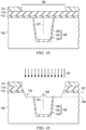
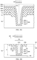
- step 230 involves forming a deep trench in a second region within the first region of the substrate.
- a deep trench (DT) etch process 121 is performed to form a deep trench 122A within a deep trench region 104, which is a second region within the first region (e.g., 106) of the substrate 102.
- the DT etch process 121 may include multiple subsequences.
- the deep trench 122A extends from and penetrating through the second and first dielectric layers 135B and 135A.
- the deep trench 122A has a trench depth d2 that is greater than a trench depth d1 of the shallow trench 133, whereas the shallow trench 133 has a trench aperture (e.g., less than the width of the ST region 106) that is wider than a trench aperture (e.g., less than the width of the DT region 104) of the deep trench 122A.
- the sequence of forming a deep trench after a shallow trench also helps prevent cone formation. As shown in subsequent figures, this is because the deep trench filler structure 126A is no longer etched and then covered by the shallow trench dielectric layer (e.g., 135A and 135B), which reduces the chances that the etch contaminants to be trapped and built up within the DT filler seam 127A of the DT structure 129A.
- the shallow trench dielectric layer e.g., 135A and 135B
- step 240 involves forming a dielectric liner interfacing the dielectric layer in the shallow trench and a sidewall of the deep trench.
- a DT oxide liner 124A is deposited onto the etched sidewalls of the dielectric layers 135A and 135B and onto the sidewall of the deep trench 122A under a dielectric liner deposition process 123.
- the dielectric liner deposition 123 may include a sub-atmospheric chemical vapor deposition of an oxide target.
- step 250 which involves forming a filler structure laterally surrounded by the dielectric layer in the shallow trench and a sidewall of the deep trench.
- a polysilicon deposition process 125 is performed to fill the deep trench 122A with a conductive material.
- a DT filler structure 126A is formed in the deep trench 122A.
- the DT filler structure 126A may contact the DT oxide liner 124A and be laterally surrounded by the dielectric layers 134A and 135B.
- a DT filler seam 127A is formed along a vertical middle section of the FT filler structure 126A.
- the dimensions of the DT filler seam 127A may depend on the aspect ratio of the deep trench 122A. Unlike the DT filler seam 127 as shown and described in FIGS.1F -1G , the DT filler seam 127A will not be subjected to further etching. As such, the DT filler seam 127A is unlikely to contribute to subsequent cone formations as shown and described in FIG. 1G .
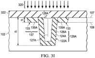
- a chemical mechanical polish process is performed to remove excessive polysilicon material above the deep trench 122.
- a chemical mechanical polish process 310 is performed to remove the remaining nitride cap layer 114 and pad oxide layer 112.
- the semiconductor device 300 includes a deep trench structure 129A extending downward and within a shallow trench structure 137.
- the shallow trench structure 137 includes a shallow trench dielectric layer 135A that extends from a first plane 107 that aligns with a top surface of the substrate 102.
- the shallow trench structure 137 further extends into the substrate 102 by a first depth d1.
- the deep trench structure 129A extends from the first plane 107 that aligns with a top surface of the substrate 102.
- the deep trench structure 129 penetrates through the shallow trench dielectric layer 135A and a second plane 108 that aligns with the bottom surface of the shallow trench 133.
- the deep trench structure 129 further extends into the substrate 102 by a second depth d2, which is greater than the first depth d1.
- the DT filler structure 126A of the deep trench structure 129A includes a polysilicon plate having an upper portion and a lower portion.
- the upper portion has a first width, and it is positioned within in the shallow trench 133.
- the lower portion has a second width, and it is positioned within in the deep trench 122A.
- the first width is greater than the second width.
- the DT oxide liner 124A interfaces between the upper portion of the polysilicon plate and the shallow trench dielectric layer 135A.
- the DT oxide liner 124A also interfaces between the lower portion of the polysilicon plate and the substrate 102.
- the DT oxide liner 124A has a lower oxide density than the shallow trench dielectric layer 135A.
- the semiconductor device 300 is substantially cone free around the top surface of the deep trench structure 129 as well as the shallow trench structure 137.
- the semiconductor device 300 can be prepared for further processing, which may include the formation of one or more dielectric layers above the deep trench structure 129 as well as the shallow trench structure 137.
- a dielectric deposition process 320 may be performed to form a dielectric layer 322 that covers a DT top surface 128A as well as a top surface of the substrate 102 and the shallow trench structure 137. In the event that the DT filler structure 126A is not further etched, any subsequent deposition of dielectric layer is unlikely to cause any cone formation thereon.
- the term “configured to” describes structural and functional characteristics of one or more tangible non-transitory components.
- the term “configured to” can be understood as having a particular configuration that is designed or dedicated for performing a certain function.
- a device is “configured to” perform a certain function if such device includes tangible non-transitory components that can be enabled, activated or powered to perform that certain function.
- the term “configured to” may encompass being configurable, but it does not require a described device to be configurable at any given point of time.
- relativity such as “about,” “approximately,” “substantially,” “near,” “within a proximity,” “sufficient . . . to,” “maximum,” and “minimum,” as applied to features of an integrated circuit and/or a semiconductor device can be understood with respect to the fabrication tolerances of a particular process for fabricating the integrated circuit and/or the semiconductor device. Also, these terms of relativity can be understood within a framework for performing one or more functions by the integrated circuit and/or the semiconductor device.
- a first resistor may have a first resistance that is substantially equal to a second resistance of the second resistor where the first and second resistors are purported to have the same resistance, yet the fabrication process introduces slight variations between the first resistance and the second resistance.
- the first resistance can be substantially equal to the second resistance even when the fabricated first and second resistors demonstrate slight difference in resistance. This slight difference may be within 5% of the design target.
- a first resistor may have a first resistance that is substantially equal to a second resistance of a second resistor where the process variations are known a priori, such that the first resistance and the second resistance can be preset at slightly different values to account for the known process variations.
- the first resistance can be substantially equal to the second resistance even when the design values of the first and second resistance are preset to include a slight difference to account for the known process variations. This slight difference may be within 5% of the design target.
Landscapes
- Element Separation (AREA)
- Metal-Oxide And Bipolar Metal-Oxide Semiconductor Integrated Circuits (AREA)
Applications Claiming Priority (2)
| Application Number | Priority Date | Filing Date | Title |
|---|---|---|---|
| US15/901,449 US10879106B2 (en) | 2018-02-21 | 2018-02-21 | Apparatus with overlapping deep trench and shallow trench and method of fabricating the same with low defect density |
| PCT/US2019/019005 WO2019165107A1 (en) | 2018-02-21 | 2019-02-21 | Apparatus with overlapping deep trench and shallow trench and method of fabricating the same with low defect density |
Publications (3)
| Publication Number | Publication Date |
|---|---|
| EP3756213A1 EP3756213A1 (en) | 2020-12-30 |
| EP3756213A4 EP3756213A4 (en) | 2021-04-28 |
| EP3756213B1 true EP3756213B1 (en) | 2025-05-21 |
Family
ID=67616963
Family Applications (1)
| Application Number | Title | Priority Date | Filing Date |
|---|---|---|---|
| EP19757672.1A Active EP3756213B1 (en) | 2018-02-21 | 2019-02-21 | Apparatus with overlapping deep trench and shallow trench and method of fabricating the same with low defect density |
Country Status (5)
| Country | Link |
|---|---|
| US (2) | US10879106B2 (https=) |
| EP (1) | EP3756213B1 (https=) |
| JP (2) | JP7755114B2 (https=) |
| CN (1) | CN112204705A (https=) |
| WO (1) | WO2019165107A1 (https=) |
Families Citing this family (10)
| Publication number | Priority date | Publication date | Assignee | Title |
|---|---|---|---|---|
| US10879106B2 (en) * | 2018-02-21 | 2020-12-29 | Texas Instruments Incorporated | Apparatus with overlapping deep trench and shallow trench and method of fabricating the same with low defect density |
| US11443976B2 (en) | 2020-10-20 | 2022-09-13 | Taiwan Semiconductor Manufacturing Company, Ltd. | Trench isolation process |
| US11410873B2 (en) * | 2020-11-20 | 2022-08-09 | Applied Materials, Inc. | Deep trench integration processes and devices |
| US11264457B1 (en) * | 2020-11-20 | 2022-03-01 | Globalfoundries U.S. Inc. | Isolation trenches augmented with a trap-rich layer |
| CN112750752B (zh) * | 2021-01-22 | 2023-06-02 | 上海华虹宏力半导体制造有限公司 | 深沟槽隔离结构的形成方法及半导体器件的形成方法 |
| US12354904B2 (en) * | 2021-10-27 | 2025-07-08 | Texas Instruments Incorporated | Method of reducing integrated deep trench optically sensitive defectivity |
| CN114242649B (zh) * | 2021-12-16 | 2026-02-03 | 上海华虹宏力半导体制造有限公司 | 高压ldmos器件及其制备方法 |
| CN114242650A (zh) * | 2021-12-16 | 2022-03-25 | 上海华虹宏力半导体制造有限公司 | 高压ldmos器件及其制备方法 |
| CN117976607B (zh) * | 2024-03-27 | 2024-06-21 | 粤芯半导体技术股份有限公司 | 半导体器件的沟槽隔离制备方法以及半导体器件 |
| CN121194505A (zh) * | 2025-11-20 | 2025-12-23 | 杭州富芯半导体有限公司 | 一种双极元件-cmos-dmos半导体器件的制备方法及半导体器件 |
Family Cites Families (30)
| Publication number | Priority date | Publication date | Assignee | Title |
|---|---|---|---|---|
| JPS60124840A (ja) * | 1983-12-09 | 1985-07-03 | Fujitsu Ltd | 半導体装置の製造方法 |
| US4579812A (en) * | 1984-02-03 | 1986-04-01 | Advanced Micro Devices, Inc. | Process for forming slots of different types in self-aligned relationship using a latent image mask |
| JPH02248063A (ja) * | 1989-03-20 | 1990-10-03 | Fujitsu Ltd | 半導体装置及びその製造方法 |
| US5972777A (en) * | 1997-07-23 | 1999-10-26 | Taiwan Semiconductor Manufacturing Company, Ltd. | Method of forming isolation by nitrogen implant to reduce bird's beak |
| US5895253A (en) * | 1997-08-22 | 1999-04-20 | Micron Technology, Inc. | Trench isolation for CMOS devices |
| US6214696B1 (en) * | 1998-04-22 | 2001-04-10 | Texas Instruments - Acer Incorporated | Method of fabricating deep-shallow trench isolation |
| US6110797A (en) * | 1999-12-06 | 2000-08-29 | National Semiconductor Corporation | Process for fabricating trench isolation structure for integrated circuits |
| JP4416527B2 (ja) * | 2003-02-07 | 2010-02-17 | 三洋電機株式会社 | 半導体装置の製造方法 |
| US7015086B2 (en) * | 2004-02-05 | 2006-03-21 | Taiwan Semiconductor Manufacturing Company, Ltd. | Method of forming a shallow trench-deep trench isolation region for a BiCMOS/CMOS technology |
| US7205630B2 (en) * | 2004-07-12 | 2007-04-17 | Taiwan Semiconductor Manufacturing Company, Ltd. | Method and apparatus for a semiconductor device having low and high voltage transistors |
| JP4646743B2 (ja) | 2004-09-08 | 2011-03-09 | 三洋電機株式会社 | 半導体装置の製造方法 |
| US8053823B2 (en) * | 2005-03-08 | 2011-11-08 | International Business Machines Corporation | Simplified buried plate structure and process for semiconductor-on-insulator chip |
| DE102005010944B4 (de) * | 2005-03-10 | 2009-09-10 | X-Fab Semiconductor Foundries Ag | Verfahren zur Herstellung eines Trägerscheibenkontaktes in integrierten Schaltungen mit Hochspannungsbauelementen auf der Basis der SOI-Technologie und integrierte Schaltungen mit entsprechenden Grabenstrukturen |
| US7361534B2 (en) | 2005-05-11 | 2008-04-22 | Advanced Micro Devices, Inc. | Method for fabricating SOI device |
| US7709345B2 (en) * | 2006-03-07 | 2010-05-04 | Micron Technology, Inc. | Trench isolation implantation |
| US20090314963A1 (en) * | 2008-06-24 | 2009-12-24 | Tel Epion Inc. | Method for forming trench isolation |
| JP2010161241A (ja) * | 2009-01-08 | 2010-07-22 | Toyota Motor Corp | 半導体装置および半導体装置の製造方法 |
| US20110217832A1 (en) * | 2009-09-30 | 2011-09-08 | Digvijay Raorane | Method of filling a deep trench in a substrate |
| JP2011243638A (ja) | 2010-05-14 | 2011-12-01 | Sharp Corp | 半導体装置の製造方法 |
| KR101201903B1 (ko) * | 2010-07-20 | 2012-11-16 | 매그나칩 반도체 유한회사 | 반도체소자의 소자분리 구조 및 그 형성방법 |
| JP5977002B2 (ja) * | 2011-08-25 | 2016-08-24 | 東京エレクトロン株式会社 | トレンチの埋め込み方法および半導体集積回路装置の製造方法 |
| US20130292791A1 (en) * | 2012-05-01 | 2013-11-07 | Taiwan Semiconductor Manufacturing Co., Ltd. | Semiconductor device and method for forming the same |
| US8703577B1 (en) | 2012-12-17 | 2014-04-22 | United Microelectronics Corp. | Method for fabrication deep trench isolation structure |
| US9202859B1 (en) | 2014-05-27 | 2015-12-01 | Texas Instruments Incorporated | Well resistors and polysilicon resistors |
| US9887123B2 (en) * | 2014-10-24 | 2018-02-06 | Newport Fab, Llc | Structure having isolated deep substrate vias with decreased pitch and increased aspect ratio and related method |
| US9812354B2 (en) | 2015-05-15 | 2017-11-07 | Semiconductor Components Industries, Llc | Process of forming an electronic device including a material defining a void |
| KR102449901B1 (ko) | 2015-06-23 | 2022-09-30 | 삼성전자주식회사 | 집적회로 소자 및 그 제조 방법 |
| KR102532202B1 (ko) | 2016-01-22 | 2023-05-12 | 삼성전자 주식회사 | 반도체 소자 |
| US10163679B1 (en) * | 2017-05-31 | 2018-12-25 | Globalfoundries Inc. | Shallow trench isolation formation without planarization |
| US10879106B2 (en) * | 2018-02-21 | 2020-12-29 | Texas Instruments Incorporated | Apparatus with overlapping deep trench and shallow trench and method of fabricating the same with low defect density |
-
2018
- 2018-02-21 US US15/901,449 patent/US10879106B2/en active Active
-
2019
- 2019-02-21 JP JP2020544399A patent/JP7755114B2/ja active Active
- 2019-02-21 EP EP19757672.1A patent/EP3756213B1/en active Active
- 2019-02-21 WO PCT/US2019/019005 patent/WO2019165107A1/en not_active Ceased
- 2019-02-21 CN CN201980012220.7A patent/CN112204705A/zh active Pending
-
2020
- 2020-12-03 US US17/110,478 patent/US20210090941A1/en active Pending
-
2024
- 2024-03-06 JP JP2024033763A patent/JP2024063193A/ja active Pending
Also Published As
| Publication number | Publication date |
|---|---|
| US10879106B2 (en) | 2020-12-29 |
| EP3756213A4 (en) | 2021-04-28 |
| JP7755114B2 (ja) | 2025-10-16 |
| JP2021517734A (ja) | 2021-07-26 |
| JP2024063193A (ja) | 2024-05-10 |
| CN112204705A (zh) | 2021-01-08 |
| WO2019165107A1 (en) | 2019-08-29 |
| US20190259651A1 (en) | 2019-08-22 |
| WO2019165107A8 (en) | 2020-12-03 |
| US20210090941A1 (en) | 2021-03-25 |
| EP3756213A1 (en) | 2020-12-30 |
Similar Documents
| Publication | Publication Date | Title |
|---|---|---|
| EP3756213B1 (en) | Apparatus with overlapping deep trench and shallow trench and method of fabricating the same with low defect density | |
| US4876217A (en) | Method of forming semiconductor structure isolation regions | |
| TWI646629B (zh) | 用於積體電路裝置之間隔物啟用之主動隔離 | |
| US9520435B2 (en) | Image sensor illuminated and connected on its back side | |
| EP3119533B1 (en) | Cmut device and manufacturing method | |
| EP2933829B1 (en) | Method for reducing defects in shallow trench isolation | |
| CN110767743A (zh) | 半导体器件的制作方法、超结器件及其制作方法 | |
| US6214657B1 (en) | Semiconductor device isolation structure and fabrication method of semiconductor device using the same | |
| US7825507B2 (en) | Semiconductor assembly and method for forming seal ring | |
| KR100518639B1 (ko) | 반도체 소자 및 그 제조방법 | |
| US11289368B2 (en) | Semiconductor device and method for fabricating semiconductor device | |
| CN108878364A (zh) | 半导体器件及其形成方法 | |
| JP6308067B2 (ja) | 半導体装置の製造方法 | |
| US12112981B2 (en) | Semiconductor device and method for fabricating semiconductor device | |
| US7691706B2 (en) | Method of fabricating a semiconductor device | |
| CN111354630B (zh) | 半导体结构及其制造方法 | |
| US20020001933A1 (en) | MOSFET and fabrication method thereof | |
| CN112510040B (zh) | 半导体器件及其制造方法 | |
| KR100548584B1 (ko) | 게이트전극 형성방법 | |
| JP4230756B2 (ja) | 半導体装置及びその製造方法。 | |
| TWI283068B (en) | Integrated circuit chip, semiconductor structure and method of manufacturing the same | |
| CN117673089A (zh) | 半导体结构及其制作方法 | |
| JPH0497516A (ja) | 半導体装置の素子分離用酸化膜形成方法 | |
| CN112825315A (zh) | 半导体结构及其形成方法 | |
| JPS62186546A (ja) | 半導体装置の製造方法 |
Legal Events
| Date | Code | Title | Description |
|---|---|---|---|
| STAA | Information on the status of an ep patent application or granted ep patent |
Free format text: STATUS: THE INTERNATIONAL PUBLICATION HAS BEEN MADE |
|
| PUAI | Public reference made under article 153(3) epc to a published international application that has entered the european phase |
Free format text: ORIGINAL CODE: 0009012 |
|
| STAA | Information on the status of an ep patent application or granted ep patent |
Free format text: STATUS: REQUEST FOR EXAMINATION WAS MADE |
|
| 17P | Request for examination filed |
Effective date: 20200921 |
|
| AK | Designated contracting states |
Kind code of ref document: A1 Designated state(s): AL AT BE BG CH CY CZ DE DK EE ES FI FR GB GR HR HU IE IS IT LI LT LU LV MC MK MT NL NO PL PT RO RS SE SI SK SM TR |
|
| AX | Request for extension of the european patent |
Extension state: BA ME |
|
| RAP1 | Party data changed (applicant data changed or rights of an application transferred) |
Owner name: TEXAS INSTRUMENTS INCORPORATED |
|
| REG | Reference to a national code |
Ref country code: DE Ref legal event code: R079 Free format text: PREVIOUS MAIN CLASS: H01L0021020000 Ipc: H01L0021762000 Ref document number: 602019070259 Country of ref document: DE |
|
| A4 | Supplementary search report drawn up and despatched |
Effective date: 20210331 |
|
| RIC1 | Information provided on ipc code assigned before grant |
Ipc: H01L 21/762 20060101AFI20210325BHEP |
|
| DAV | Request for validation of the european patent (deleted) | ||
| DAX | Request for extension of the european patent (deleted) | ||
| STAA | Information on the status of an ep patent application or granted ep patent |
Free format text: STATUS: EXAMINATION IS IN PROGRESS |
|
| 17Q | First examination report despatched |
Effective date: 20231121 |
|
| RIC1 | Information provided on ipc code assigned before grant |
Ipc: H01L 21/308 20060101ALI20240802BHEP Ipc: H01L 21/762 20060101AFI20240802BHEP |
|
| GRAP | Despatch of communication of intention to grant a patent |
Free format text: ORIGINAL CODE: EPIDOSNIGR1 |
|
| STAA | Information on the status of an ep patent application or granted ep patent |
Free format text: STATUS: GRANT OF PATENT IS INTENDED |
|
| INTG | Intention to grant announced |
Effective date: 20241223 |
|
| P01 | Opt-out of the competence of the unified patent court (upc) registered |
Free format text: CASE NUMBER: APP_2102/2025 Effective date: 20250113 |
|
| GRAS | Grant fee paid |
Free format text: ORIGINAL CODE: EPIDOSNIGR3 |
|
| GRAA | (expected) grant |
Free format text: ORIGINAL CODE: 0009210 |
|
| STAA | Information on the status of an ep patent application or granted ep patent |
Free format text: STATUS: THE PATENT HAS BEEN GRANTED |
|
| AK | Designated contracting states |
Kind code of ref document: B1 Designated state(s): AL AT BE BG CH CY CZ DE DK EE ES FI FR GB GR HR HU IE IS IT LI LT LU LV MC MK MT NL NO PL PT RO RS SE SI SK SM TR |
|
| REG | Reference to a national code |
Ref country code: GB Ref legal event code: FG4D |
|
| REG | Reference to a national code |
Ref country code: CH Ref legal event code: EP |
|
| REG | Reference to a national code |
Ref country code: DE Ref legal event code: R096 Ref document number: 602019070259 Country of ref document: DE |
|
| REG | Reference to a national code |
Ref country code: IE Ref legal event code: FG4D |
|
| REG | Reference to a national code |
Ref country code: NL Ref legal event code: MP Effective date: 20250521 |
|
| PG25 | Lapsed in a contracting state [announced via postgrant information from national office to epo] |
Ref country code: PT Free format text: LAPSE BECAUSE OF FAILURE TO SUBMIT A TRANSLATION OF THE DESCRIPTION OR TO PAY THE FEE WITHIN THE PRESCRIBED TIME-LIMIT Effective date: 20250922 Ref country code: FI Free format text: LAPSE BECAUSE OF FAILURE TO SUBMIT A TRANSLATION OF THE DESCRIPTION OR TO PAY THE FEE WITHIN THE PRESCRIBED TIME-LIMIT Effective date: 20250521 Ref country code: ES Free format text: LAPSE BECAUSE OF FAILURE TO SUBMIT A TRANSLATION OF THE DESCRIPTION OR TO PAY THE FEE WITHIN THE PRESCRIBED TIME-LIMIT Effective date: 20250521 |
|
| REG | Reference to a national code |
Ref country code: LT Ref legal event code: MG9D |
|
| PG25 | Lapsed in a contracting state [announced via postgrant information from national office to epo] |
Ref country code: NO Free format text: LAPSE BECAUSE OF FAILURE TO SUBMIT A TRANSLATION OF THE DESCRIPTION OR TO PAY THE FEE WITHIN THE PRESCRIBED TIME-LIMIT Effective date: 20250821 Ref country code: GR Free format text: LAPSE BECAUSE OF FAILURE TO SUBMIT A TRANSLATION OF THE DESCRIPTION OR TO PAY THE FEE WITHIN THE PRESCRIBED TIME-LIMIT Effective date: 20250822 |
|
| PG25 | Lapsed in a contracting state [announced via postgrant information from national office to epo] |
Ref country code: NL Free format text: LAPSE BECAUSE OF FAILURE TO SUBMIT A TRANSLATION OF THE DESCRIPTION OR TO PAY THE FEE WITHIN THE PRESCRIBED TIME-LIMIT Effective date: 20250521 Ref country code: PL Free format text: LAPSE BECAUSE OF FAILURE TO SUBMIT A TRANSLATION OF THE DESCRIPTION OR TO PAY THE FEE WITHIN THE PRESCRIBED TIME-LIMIT Effective date: 20250521 |
|
| PG25 | Lapsed in a contracting state [announced via postgrant information from national office to epo] |
Ref country code: BG Free format text: LAPSE BECAUSE OF FAILURE TO SUBMIT A TRANSLATION OF THE DESCRIPTION OR TO PAY THE FEE WITHIN THE PRESCRIBED TIME-LIMIT Effective date: 20250521 |
|
| PG25 | Lapsed in a contracting state [announced via postgrant information from national office to epo] |
Ref country code: HR Free format text: LAPSE BECAUSE OF FAILURE TO SUBMIT A TRANSLATION OF THE DESCRIPTION OR TO PAY THE FEE WITHIN THE PRESCRIBED TIME-LIMIT Effective date: 20250521 |
|
| PG25 | Lapsed in a contracting state [announced via postgrant information from national office to epo] |
Ref country code: RS Free format text: LAPSE BECAUSE OF FAILURE TO SUBMIT A TRANSLATION OF THE DESCRIPTION OR TO PAY THE FEE WITHIN THE PRESCRIBED TIME-LIMIT Effective date: 20250821 |
|
| PG25 | Lapsed in a contracting state [announced via postgrant information from national office to epo] |
Ref country code: IS Free format text: LAPSE BECAUSE OF FAILURE TO SUBMIT A TRANSLATION OF THE DESCRIPTION OR TO PAY THE FEE WITHIN THE PRESCRIBED TIME-LIMIT Effective date: 20250921 |
|
| PG25 | Lapsed in a contracting state [announced via postgrant information from national office to epo] |
Ref country code: LV Free format text: LAPSE BECAUSE OF FAILURE TO SUBMIT A TRANSLATION OF THE DESCRIPTION OR TO PAY THE FEE WITHIN THE PRESCRIBED TIME-LIMIT Effective date: 20250521 |
|
| REG | Reference to a national code |
Ref country code: DE Ref legal event code: R079 Ref document number: 602019070259 Country of ref document: DE Free format text: PREVIOUS MAIN CLASS: H01L0021762000 Ipc: H10W0010100000 |
|
| REG | Reference to a national code |
Ref country code: AT Ref legal event code: MK05 Ref document number: 1797550 Country of ref document: AT Kind code of ref document: T Effective date: 20250521 |
|
| PG25 | Lapsed in a contracting state [announced via postgrant information from national office to epo] |
Ref country code: DK Free format text: LAPSE BECAUSE OF FAILURE TO SUBMIT A TRANSLATION OF THE DESCRIPTION OR TO PAY THE FEE WITHIN THE PRESCRIBED TIME-LIMIT Effective date: 20250521 Ref country code: AT Free format text: LAPSE BECAUSE OF FAILURE TO SUBMIT A TRANSLATION OF THE DESCRIPTION OR TO PAY THE FEE WITHIN THE PRESCRIBED TIME-LIMIT Effective date: 20250521 Ref country code: SM Free format text: LAPSE BECAUSE OF FAILURE TO SUBMIT A TRANSLATION OF THE DESCRIPTION OR TO PAY THE FEE WITHIN THE PRESCRIBED TIME-LIMIT Effective date: 20250521 |
|
| PG25 | Lapsed in a contracting state [announced via postgrant information from national office to epo] |
Ref country code: CZ Free format text: LAPSE BECAUSE OF FAILURE TO SUBMIT A TRANSLATION OF THE DESCRIPTION OR TO PAY THE FEE WITHIN THE PRESCRIBED TIME-LIMIT Effective date: 20250521 |
|
| PG25 | Lapsed in a contracting state [announced via postgrant information from national office to epo] |
Ref country code: EE Free format text: LAPSE BECAUSE OF FAILURE TO SUBMIT A TRANSLATION OF THE DESCRIPTION OR TO PAY THE FEE WITHIN THE PRESCRIBED TIME-LIMIT Effective date: 20250521 |
|
| PG25 | Lapsed in a contracting state [announced via postgrant information from national office to epo] |
Ref country code: SK Free format text: LAPSE BECAUSE OF FAILURE TO SUBMIT A TRANSLATION OF THE DESCRIPTION OR TO PAY THE FEE WITHIN THE PRESCRIBED TIME-LIMIT Effective date: 20250521 Ref country code: RO Free format text: LAPSE BECAUSE OF FAILURE TO SUBMIT A TRANSLATION OF THE DESCRIPTION OR TO PAY THE FEE WITHIN THE PRESCRIBED TIME-LIMIT Effective date: 20250521 |
|
| PG25 | Lapsed in a contracting state [announced via postgrant information from national office to epo] |
Ref country code: IT Free format text: LAPSE BECAUSE OF FAILURE TO SUBMIT A TRANSLATION OF THE DESCRIPTION OR TO PAY THE FEE WITHIN THE PRESCRIBED TIME-LIMIT Effective date: 20250521 |
|
| REG | Reference to a national code |
Ref country code: DE Ref legal event code: R097 Ref document number: 602019070259 Country of ref document: DE |
|
| PLBE | No opposition filed within time limit |
Free format text: ORIGINAL CODE: 0009261 |
|
| STAA | Information on the status of an ep patent application or granted ep patent |
Free format text: STATUS: NO OPPOSITION FILED WITHIN TIME LIMIT |
|
| REG | Reference to a national code |
Ref country code: CH Ref legal event code: L10 Free format text: ST27 STATUS EVENT CODE: U-0-0-L10-L00 (AS PROVIDED BY THE NATIONAL OFFICE) Effective date: 20260402 |
|
| PGFP | Annual fee paid to national office [announced via postgrant information from national office to epo] |
Ref country code: GB Payment date: 20260121 Year of fee payment: 8 |
|
| PGFP | Annual fee paid to national office [announced via postgrant information from national office to epo] |
Ref country code: DE Payment date: 20260121 Year of fee payment: 8 |
|
| PGFP | Annual fee paid to national office [announced via postgrant information from national office to epo] |
Ref country code: FR Payment date: 20260121 Year of fee payment: 8 |
|
| 26N | No opposition filed |
Effective date: 20260224 |