EP3754638B1 - Schieberegistereinheit, gate-ansteuerungsvorrichtung, anzeigevorrichtung und ansteuerungsverfahren - Google Patents
Schieberegistereinheit, gate-ansteuerungsvorrichtung, anzeigevorrichtung und ansteuerungsverfahren Download PDFInfo
- Publication number
- EP3754638B1 EP3754638B1 EP18906612.9A EP18906612A EP3754638B1 EP 3754638 B1 EP3754638 B1 EP 3754638B1 EP 18906612 A EP18906612 A EP 18906612A EP 3754638 B1 EP3754638 B1 EP 3754638B1
- Authority
- EP
- European Patent Office
- Prior art keywords
- transistor
- signal
- coupled
- node
- circuit
- Prior art date
- Legal status (The legal status is an assumption and is not a legal conclusion. Google has not performed a legal analysis and makes no representation as to the accuracy of the status listed.)
- Active
Links
Images


Classifications
-
- G—PHYSICS
- G09—EDUCATION; CRYPTOGRAPHY; DISPLAY; ADVERTISING; SEALS
- G09G—ARRANGEMENTS OR CIRCUITS FOR CONTROL OF INDICATING DEVICES USING STATIC MEANS TO PRESENT VARIABLE INFORMATION
- G09G3/00—Control arrangements or circuits, of interest only in connection with visual indicators other than cathode-ray tubes
- G09G3/20—Control arrangements or circuits, of interest only in connection with visual indicators other than cathode-ray tubes for presentation of an assembly of a number of characters, e.g. a page, by composing the assembly by combination of individual elements arranged in a matrix no fixed position being assigned to or needed to be assigned to the individual characters or partial characters
- G09G3/22—Control arrangements or circuits, of interest only in connection with visual indicators other than cathode-ray tubes for presentation of an assembly of a number of characters, e.g. a page, by composing the assembly by combination of individual elements arranged in a matrix no fixed position being assigned to or needed to be assigned to the individual characters or partial characters using controlled light sources
- G09G3/30—Control arrangements or circuits, of interest only in connection with visual indicators other than cathode-ray tubes for presentation of an assembly of a number of characters, e.g. a page, by composing the assembly by combination of individual elements arranged in a matrix no fixed position being assigned to or needed to be assigned to the individual characters or partial characters using controlled light sources using electroluminescent panels
- G09G3/32—Control arrangements or circuits, of interest only in connection with visual indicators other than cathode-ray tubes for presentation of an assembly of a number of characters, e.g. a page, by composing the assembly by combination of individual elements arranged in a matrix no fixed position being assigned to or needed to be assigned to the individual characters or partial characters using controlled light sources using electroluminescent panels semiconductive, e.g. using light-emitting diodes [LED]
- G09G3/3208—Control arrangements or circuits, of interest only in connection with visual indicators other than cathode-ray tubes for presentation of an assembly of a number of characters, e.g. a page, by composing the assembly by combination of individual elements arranged in a matrix no fixed position being assigned to or needed to be assigned to the individual characters or partial characters using controlled light sources using electroluminescent panels semiconductive, e.g. using light-emitting diodes [LED] organic, e.g. using organic light-emitting diodes [OLED]
- G09G3/3266—Details of drivers for scan electrodes
-
- G—PHYSICS
- G09—EDUCATION; CRYPTOGRAPHY; DISPLAY; ADVERTISING; SEALS
- G09G—ARRANGEMENTS OR CIRCUITS FOR CONTROL OF INDICATING DEVICES USING STATIC MEANS TO PRESENT VARIABLE INFORMATION
- G09G3/00—Control arrangements or circuits, of interest only in connection with visual indicators other than cathode-ray tubes
- G09G3/20—Control arrangements or circuits, of interest only in connection with visual indicators other than cathode-ray tubes for presentation of an assembly of a number of characters, e.g. a page, by composing the assembly by combination of individual elements arranged in a matrix no fixed position being assigned to or needed to be assigned to the individual characters or partial characters
- G09G3/22—Control arrangements or circuits, of interest only in connection with visual indicators other than cathode-ray tubes for presentation of an assembly of a number of characters, e.g. a page, by composing the assembly by combination of individual elements arranged in a matrix no fixed position being assigned to or needed to be assigned to the individual characters or partial characters using controlled light sources
- G09G3/30—Control arrangements or circuits, of interest only in connection with visual indicators other than cathode-ray tubes for presentation of an assembly of a number of characters, e.g. a page, by composing the assembly by combination of individual elements arranged in a matrix no fixed position being assigned to or needed to be assigned to the individual characters or partial characters using controlled light sources using electroluminescent panels
- G09G3/32—Control arrangements or circuits, of interest only in connection with visual indicators other than cathode-ray tubes for presentation of an assembly of a number of characters, e.g. a page, by composing the assembly by combination of individual elements arranged in a matrix no fixed position being assigned to or needed to be assigned to the individual characters or partial characters using controlled light sources using electroluminescent panels semiconductive, e.g. using light-emitting diodes [LED]
- G09G3/3208—Control arrangements or circuits, of interest only in connection with visual indicators other than cathode-ray tubes for presentation of an assembly of a number of characters, e.g. a page, by composing the assembly by combination of individual elements arranged in a matrix no fixed position being assigned to or needed to be assigned to the individual characters or partial characters using controlled light sources using electroluminescent panels semiconductive, e.g. using light-emitting diodes [LED] organic, e.g. using organic light-emitting diodes [OLED]
-
- G—PHYSICS
- G11—INFORMATION STORAGE
- G11C—STATIC STORES
- G11C19/00—Digital stores in which the information is moved stepwise, e.g. shift registers
- G11C19/28—Digital stores in which the information is moved stepwise, e.g. shift registers using semiconductor elements
-
- G—PHYSICS
- G09—EDUCATION; CRYPTOGRAPHY; DISPLAY; ADVERTISING; SEALS
- G09G—ARRANGEMENTS OR CIRCUITS FOR CONTROL OF INDICATING DEVICES USING STATIC MEANS TO PRESENT VARIABLE INFORMATION
- G09G2300/00—Aspects of the constitution of display devices
- G09G2300/04—Structural and physical details of display devices
- G09G2300/0421—Structural details of the set of electrodes
- G09G2300/0426—Layout of electrodes and connections
-
- G—PHYSICS
- G09—EDUCATION; CRYPTOGRAPHY; DISPLAY; ADVERTISING; SEALS
- G09G—ARRANGEMENTS OR CIRCUITS FOR CONTROL OF INDICATING DEVICES USING STATIC MEANS TO PRESENT VARIABLE INFORMATION
- G09G2310/00—Command of the display device
- G09G2310/02—Addressing, scanning or driving the display screen or processing steps related thereto
- G09G2310/0264—Details of driving circuits
- G09G2310/0286—Details of a shift registers arranged for use in a driving circuit
-
- G—PHYSICS
- G09—EDUCATION; CRYPTOGRAPHY; DISPLAY; ADVERTISING; SEALS
- G09G—ARRANGEMENTS OR CIRCUITS FOR CONTROL OF INDICATING DEVICES USING STATIC MEANS TO PRESENT VARIABLE INFORMATION
- G09G2310/00—Command of the display device
- G09G2310/08—Details of timing specific for flat panels, other than clock recovery
Definitions
- Embodiments of the present disclosure relate to a shift register unit, a gate driving circuit, a display device and a driving method.
- US2017039950A1 discloses a shift register unit having a pulse width modulation module which includes a first input submodule, a first pull-down submodule, a second input submodule, a second pull-down submodule, a third input submodule, and a third pull-down submodule.
- the shift register unit also includes a feedback signal from its output to the input submodule.
- CN107039017A , KR20170078978A and US2015030116A1 are further examples of known shift register units for a display.
- Coupled or “connected” and the like are not restricted to physical or mechanical connections, but may include electrical connections, whether direct or indirect.
- Words “upper”, “lower”, “left”, “right”, and the like are used merely to indicate relative positional relationships, and when an absolute position of an object being described is changed, the relative positional relationships may also be changed accordingly.
- the term "pull-up” means charging a node or an electrode of a transistor such that an absolute value of a level of the node or the electrode is raised, thereby implementing an operation (e.g., turning on) of the corresponding transistor;
- pulse-down means discharging a node or an electrode of a transistor so that an absolute value of a level of the node or the electrode is lowered, thereby achieving an operation (e.g., turning off) of the corresponding transistor.
- a gate driving circuit for an OLED is usually formed by combining three sub-circuits, namely a detection circuit, a display circuit and a connection circuit (or gate circuit) for outputting a composite pulse of the detection circuit and the display circuit, and such a circuit structure is very complex and cannot meet the requirements for high resolution and narrow bezel.
- an external compensation may be performed by providing sensing transistors.
- the gate driving circuit constituted by the shift register units needs to supply driving signals for scanning transistors and the sensing transistors, for example, scanning driving signals for the scanning transistors supplied n a display period (Display) of one frame, and sensing driving signals for the sensing transistors in a blanking period (Blank) of the frame, to the sub-pixel units in the display panel, respectively.
- the sensing driving signals output by the gate driving circuit are used to sequentially scan row-by-row, for example, the sensing driving signal for the sub-pixel units of a first row in the display panel is output in the blanking period of a first frame, the sensing driving signal for the sub-pixel units of a second row in the display panel is output in a blanking period of a second frame, and so on, thus the sensing driving signals are sequentially output row-by-row at a frequency that one sensing driving signal corresponding to the sub-pixel units of one row is output per frame, that is, the progressive sequential compensation for the display panel is completed.
- a display failure problem occurs: firstly, a scanning line moving row-by-row occurs in the process of scanning and displaying multiple frames; secondly, a difference of time points of performing the external compensation may cause brightness difference of different areas of the display panel to be relatively large, for example, when the externally compensation is performed on the sub-pixel units of the 100th row of the display panel, although the externally compensation has been already performed on the sub-pixel units of the 10th row of the display panel, the light emitting brightness of the sub-pixel units of the 10th row may have been changed, for example, the brightness is reduced, so that the brightnesses of different areas of the display panel may be de-uniform, and thus such a problem may be more obvious in a large-sized display panel.
- At least one embodiment of the present disclosure provides a shift register unit including a blanking input circuit, a display input circuit, an output circuit, and a compensation selection circuit.
- the blanking input circuit is configured to input a blanking input signal to a control node and to input a blanking signal to a first node during a blanking period of one frame;
- the display input circuit is configured to input a display signal to the first node in a display period of the frame in response to a display input signal;
- the output circuit is configured to output a composite output signal to an output terminal under the control of a level of the first node;
- the compensation selection circuit is electrically coupled with the output terminal and is configured to charge the control node by utilizing the composite output signal in response to a compensation selection control signal.
- the embodiments of the present disclosure also provide a gate driving circuit, a display device and a driving method corresponding to the shift register unit.
- the shift register unit, the gate driving circuit, the display device and the driving method provided by the embodiments of the present disclosure can also realize a random compensation on the premise of considering the progressive sequential compensation (for example, the progressive sequential compensation is required in a shutdown detection), so that the display defects such as scanning line and de-uniform display brightness caused by the progressive sequential compensation can be avoided.
- the progressive sequential compensation for example, the progressive sequential compensation is required in a shutdown detection
- the random compensation refers to an external compensation method different from the progressive sequential compensation method, and the sensing driving signal corresponding to the sub-pixel units of any row of the display panel can be randomly output in the blanking period of a certain frame, the following embodiments are the same as above, and are not described again.
- one frame includes a display period and a blanking period that are sequentially performed, for example, in the display period, the gate driving circuit outputs a display output signal that can drive the display panel to complete scanning and displaying of a complete image from the first row to the last row, and in the blanking period, the gate driving circuit outputs a blanking output signal that can be used to drive the sensing transistor in a certain row of sub-pixel units in the display panel to complete the external compensation of the certain row of sub-pixel units.
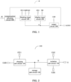
- the shift register unit 10 includes a blanking input circuit 100, a display input circuit 200, an output circuit 300, and a compensation selection circuit 400.
- the blanking input circuit 100, the display input circuit 200, and the output circuit 300 are coupled together through a first node Q.
- the blanking input circuit 100 is configured to input a blanking input signal to a control node H (not shown in Fig. 1 , see Fig. 2 ) and to input a blanking signal to the first node Q in a blanking period of one frame.
- the blanking input circuit 100 may be coupled to a blanking input signal terminal STU1 and a second clock signal terminal CLKB, so that the blanking input signal input from the blanking input signal terminal STU1 may be input to the control node H under the control of a second clock signal input from the second clock signal terminal CLKB.
- the blanking input circuit 100 may also be coupled to the third clock signal terminal CLKC so that a third clock signal input from the third clock signal terminal CLKC is input to the first node Q as a blanking signal in a blanking period of one frame, thereby pulling up a potential of the first node Q to an operating potential.
- the blanking input circuit 100 may receive and store the blanking input signal in a display period of one frame, and output the blanking signal to the first node Q in accordance with the blanking input signal in the blanking period of this frame, thereby pulling up the potential of the first node Q to the operating potential.
- the blanking input circuit 100 may receive and store the blanking input signal in the blanking period of the frame, and output the blanking signal to the first node Q according to the blanking input signal in a blanking period of a next frame, thereby pulling up the potential of the first node Q to the operating potential.
- the embodiments of the present disclosure are not limited above.
- the display input circuit 200 is configured to input a display signal to the first node Q in a display period of one frame in response to a display input signal.
- the display input circuit 200 may be coupled to a display input signal terminal STU2 to receive the display input signal, and the display input circuit 200 may be further coupled to a second voltage terminal VDD to receive a second voltage as the display signal.
- the display input circuit 200 may input the display signal to the first node Q under the control of the display input signal in the display period of the frame, thereby pulling up the potential of the first node Q to the operating potential.
- the second voltage terminal VDD is configured to output a DC high level signal, that is, the second voltage is at a high level, and the following embodiments are the same and will not be described again.
- the output circuit 300 is configured to output a composite output signal to the output terminal OUTPUT under the control of the level of the first node Q.
- the output circuit 300 may be coupled to a fourth clock signal terminal CLKD to receive a fourth clock signal as the composite output signal.
- the composite output signal includes a first output signal and a second output signal, e.g., the first output signal is a display output signal, and the second output signal is a blanking output signal.
- the output circuit 300 outputs the display output signal to the output terminal OUTPUT under the control of the level of the first node Q, for example, in some embodiments, the output terminal OUTPUT may include a shift signal output terminal CR and a pixel signal output terminal OUT, the display output signal output from the shift signal output terminal CR may be used for scan shift from a previous register unit to a next shift register unit, and the display output signal output from the pixel signal output terminal OUT may be used for driving the sub-pixel units in the display panel to perform scan display; in the blanking period of the frame, the output circuit 300 outputs a blanking output signal, which may be used to drive the sensing transistor, to the output terminal OUTPUT under the control of the level of the first node Q.
- the compensation selection circuit 400 is electrically coupled to the output terminal OUTPUT and is configured to charge the control node H by using the composite output signal in response to a compensation selection control signal.
- the compensation selection circuit 400 is configured to charge the control node H with a first output signal (e.g., the display output signal) in response to the compensation selection control signal during the display period of the frame.
- a first output signal e.g., the display output signal
- the compensation selection circuit 400 may be electrically coupled to the shift signal output terminal CR.
- the compensation selection circuit 400 may also be coupled to a compensation selection control terminal OE to receive the compensation selection control signal.
- the compensation selection circuit 400 may be disabled by inputting a signal to turn off the compensation selection circuit 400 through the compensation selection control terminal OE.
- the compensation selection control signal for turning on the compensation selection circuit 400 may be input through the compensation selection control terminal OE, and the compensation selection control signal may be configured to have the same timing as the above-described display output signal for driving the n th row of sub-pixel units; meanwhile, since the compensation selection circuit 400 is electrically coupled to the output terminal OUTPUT, the control node H in the compensation input circuit 100 may be charged with the composite output signal when the compensation selection circuit 400 is turned on, so that the control node H is charged to a high level, and thus the
- the random compensation can be achieved on the premise of achieving the progressive sequential compensation, so that display defects such as scanning lines and non-uniformity of display brightness due to progressive sequential compensation can be avoided.
- the blanking input circuit 100 includes a charging sub-circuit 110, a storage sub-circuit 120, and an isolation sub-circuit 130.
- the storage sub-circuit 120 is configured to store the blanking input signal input by the charging sub-circuit 110. For example, in the display period of the frame, the control node H is charged to a high level by the input blanking input signal, and the storage sub-circuit 120 may store the blanking input signal so that the high level of the control node H is maintained up to the blanking period of the frame.
- the isolation sub-circuit 130 is configured to input the blanking signal to the first node Q under the control of the level of the control node H and the first clock signal.
- the isolation sub-circuit 130 is coupled to the first clock signal terminal CLKA to receive the first clock signal
- the isolation sub-circuit 130 is coupled to the third clock signal terminal CLKC to receive the third clock signal as the blanking signal.
- the isolation sub-circuit 130 is turned on under the control of the level of the control node H and the first clock signal, so that the blanking signal may be input to the first node Q.
- the isolation sub-circuit 130 is disposed between the first node Q and control node H for preventing interaction of the first node Q and the control node H.
- the isolation sub-circuit 130 may disconnect the first node Q from the control node H when the blanking signal is not required to be output.
- the shift register unit 10 provided by the embodiments of the present disclosure, it is possible to control the level of the first node Q at different periods through the blanking input circuit 100 and the display input circuit 200 respectively, so that the blanking input circuit 100 and the display input circuit 200 share the same output circuit 300 to realize the output of the composite output signal.
- the shift register unit 10 may further include a first control circuit 600, and the first control circuit 600 is configured to control a level of a second node QB under the control of the level of the first node Q.
- the first control circuit 600 is coupled to a first voltage terminal VGL1 and a fourth voltage terminal VDD_A. It should be noted that, in the embodiment of the disclosure, for example, the first voltage terminal VGL1 may be configured to provide a DC low level signal, and the following embodiments are the same and will not be described again.
- the first control circuit 600 may pull down a potential of the second node QB to a low level through the first voltage terminal VGL1.
- the first control circuit 600 may charge the second node QB with a fourth voltage (e.g., at a high level) input from the fourth voltage terminal VDD_A to pull up the second node QB to a high level.
- the first control circuit 600 may be further coupled to a fifth voltage terminal VDD_B to receive a fifth voltage (e.g., at a high level), for example, the fourth voltage terminal VDD_A and the fifth voltage terminal VDD_B may be configured to alternately output a high level, that is, when the fourth voltage terminal VDD_A outputs a high level, the fifth voltage terminal VDD_B outputs a low level, and when the fourth voltage terminal VDD_A outputs a low level, the fifth voltage terminal VDD_B outputs a high level.
- a fifth voltage e.g., at a high level
- the shift register unit 10 may further include a noise reduction circuit 500, and the noise reduction circuit 500 is configured to reduce noise of the first node Q and the output terminal OUTPUT under the control of the level of the second node QB.
- the noise reduction circuit 500 is coupled to the first voltage terminal VGL1, and when the noise reduction circuit 500 is turned on under the control of the level of the second node QB, the first node Q and the Output terminal OUTPUT may be pulled down by the first voltage terminal VGL1, thereby reducing the noise of the first node Q and the output terminal OUTPUT.
- the output terminal OUTPUT includes the shift signal output terminal CR and the pixel signal output terminal OUT
- the noise reduction circuit 500 may simultaneously perform noise reduction on the shift signal output terminal CR and the pixel signal output terminal OUT.
- the shift register unit 10 may further include a second control circuit 700, and the second control circuit 700 is configured to control the level of the second node QB in response to the blanking control signal.
- the second control circuit 700 is coupled to the first clock signal terminal CLKA to receive the first clock signal as the blanking control signal, while being coupled to the first voltage terminal VGL1 to receive the first voltage at a low level.
- the second control circuit 700 may be turned on in response to the first clock signal, so that the second node QB may be pulled down by the first voltage terminal VGL1. In this way, the influence of the second node QB on the first node Q in the blanking period can be reduced, so that the blanking input circuit 100 charges the first node Q more sufficiently.
- the second control circuit 700 may also be coupled to other signal terminals to receive the blanking control signal, which is not limited by the present disclosure.
- the shift register unit 10 may further include a third control circuit 800, and the third control circuit 800 is configured to control the level of the second node QB in response to the display control signal.
- the third control circuit 800 is coupled to the display input signal terminal STU2 to receive the display input signal as the display control signal, and is coupled to the first voltage terminal VGL1 to receive the first voltage at the low level.
- the third control circuit 800 is turned on, so that the second node QB can be pulled down through the first voltage terminal VGL1. In this way, the influence of the second node QB on the first node Q can be reduced in the display period, so that the first node Q is charged more sufficiently by the display input circuit 200.
- the blanking reset circuit 900 may be turned on in response to the second clock signal, so that the first node Q may be reset through the first voltage terminal VGL 1; for another example, in the blanking period of the frame, the blanking reset circuit 900 may be turned on in response to the second clock signal, so that the first node Q may be reset through the first voltage terminal VGL 1.
- the blanking reset circuit 900 may also use other control signals as the blanking reset signal, for example, the blanking reset circuit 900 may also be coupled to other signal terminals to receive the blanking reset signal, which is not limited by the present disclosure.
- the shift register unit 10 may further include a display reset circuit 1000, and the display reset circuit 1000 is configured to reset the first node Q in response to a display reset signal.
- the display reset circuit 1000 may be coupled to a display reset signal terminal STD to receive the display reset signal, while being coupled to the first voltage terminal VGL1 to receive the first voltage of the low level.
- the display reset circuit 1000 may be turned on in response to the display reset signal, so that the first node Q may be reset through the first voltage terminal VGL1.
- the display reset signal terminal STD thereof may be coupled to a shift signal output terminal CR of the shift register unit 10 of a next stage.
- the shift register unit 10 in Fig. 3 shows to include the noise reduction circuit 500, the first control circuit 600, the second control circuit 700, the third control circuit 800, the blanking reset circuit 900 and the display reset circuit 1000, the above examples do not limit the scope of the present disclosure. In practical applications, a skilled person may choose to use or not use one or more of the above circuits according to circumstances, and various combined modifications based on the above circuits do not depart from the principle of the present disclosure, and are not described in detail here.
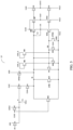
- the shift register unit 10 shown in Fig. 3 may be implemented as the circuit configuration shown in Fig. 4 .
- the shift register unit 10 includes: first to seventeenth transistors M1-M17 and first and second capacitors C1 and C2.
- the output terminal OUTPUT includes a shift signal output terminal CR and a pixel signal output terminal OUT, both of which can output a composite output signal.
- the transistors shown in Fig. 4 are all described by taking N-type transistors as an example.
- the compensation selection circuit 400 may be implemented as a first transistor M1.
- a gate of the first transistor M1 is coupled to the compensation selection control terminal OE to receive the compensation selection control signal
- a first electrode of the first transistor M1 is coupled to the shift signal output terminal CR (not shown for simplicity) to receive the composite output signal
- a second electrode of the first transistor M1 is coupled to the control node H to charge the control node H.
- the charging sub-circuit 110 in the blanking input circuit 100 may be implemented as a second transistor M2, a gate of the second transistor M2 is coupled to the second clock signal terminal CLKB to receive the second clock signal, a first electrode of the second transistor M2 is coupled to the blanking input signal terminal STU1 to receive the blanking input signal, and a second electrode of the second transistor M2 is coupled to the control node H.
- the second clock signal is a high-level turn-on signal
- the second transistor M2 is turned on under the control of the second clock signal, so that the blanking input signal may be input to the control node H to charge the control node H.
- the blanking input signal terminal STU1 of the shift register unit 10 of the (n+1) th stage may be electrically coupled to the shift signal output terminal CR of the shift register unit 10 of the n th stage, where n is an integer greater than 0.
- the storage sub-circuit 120 in the blanking input circuit 100 may be implemented as a first capacitor C1, a first electrode of the first capacitor C1 is coupled to the control node H, and a second electrode of the first capacitor C1 is coupled to the first voltage terminal VGL1 to receive the first voltage.
- the potential of the control node H can be maintained by providing the first capacitor C1, for example, in the display period of the frame, the charging sub-circuit 110 charges the control node H to a high level, and the first capacitor C1 can maintain the high level of the control node H up to the blanking period of the frame.
- the isolation sub-circuit 130 in the blanking input circuit 100 may be implemented as a third transistor M3 and a fourth transistor M4, a gate of the third transistor M3 is coupled to the control node H, a first electrode of the third transistor M3 is couple to the third clock signal terminal CLKC to receive the third clock signal as the blanking signal, a second electrode of the third transistor M3 is coupled to a first electrode of the fourth transistor M4, a gate of the fourth transistor M4 is coupled to the first clock signal terminal CLKA to receive the first clock signal, and a second electrode of the fourth transistor M4 is coupled to the first node Q.
- the third transistor M3 is turned on under the control of the control node H, and when the first clock signal is a turn-on signal at a high-level, the fourth transistor M4 is turned on under the control of the first clock signal, so that the third clock signal can charge the first node Q through the third transistor M3 and the fourth transistor M4.
- the display input circuit 200 may be implemented as a fifth transistor M5, a gate of the fifth transistor M5 is coupled to the display input signal terminal STU2 to receive the display input signal, a first electrode of the fifth transistor M5 is coupled to the second voltage terminal VDD to receive the second voltage as the display signal, and a second electrode of the fifth transistor M5 is coupled to the first node Q.
- the fifth transistor M5 is turned on under the control of the display input signal, thereby charging the first node Q with the second voltage.
- the display input signal terminal STU2 of the shift register unit 10 of the (n+2) th stage may be electrically coupled to the shift signal output terminal CR of the shift register unit 10 of the (n+1) th stage or the n th stage, where n is an integer greater than 0.
- the output circuit 300 may be implemented to include a sixth transistor M6, a seventh transistor M7, and a second capacitor.
- a gate of the sixth transistor M6 is coupled to the first node Q, a first electrode of the sixth transistor M6 is coupled to the fourth clock signal terminal CLKD to receive the fourth clock signal as the composite output signal, and a second electrode of the sixth transistor M6 is coupled to the shift signal output terminal CR;
- a gate of the seventh transistor M7 is coupled to the first node Q, a first electrode of the seventh transistor M7 is coupled to the fourth clock signal terminal CLKD to receive the fourth clock signal as the composite output signal, and a second electrode of the seventh transistor M7 is coupled to the pixel signal output terminal OUT;
- a first electrode of the second capacitor C2 is coupled to the first node Q, and a second electrode of the second capacitor C2 is coupled to the second electrode of the sixth transistor M6.
- the sixth transistor M6 and the seventh transistor M7 are turned on, so that the fourth clock signal can be output to the shift signal output terminal CR and the pixel signal output terminal OUT as the composite output signal.
- the first control circuit 600 may be implemented to include an eighth transistor M8, a ninth transistor M9, and a tenth transistor M10.
- a gate and a first electrode of the eighth transistor M8 are coupled together and configured to be coupled to the fourth voltage terminal VDD_A to receive the fourth voltage, and a second electrode of the eighth transistor M8 is coupled to the second node QB;
- a gate and a first electrode of the ninth transistor M9 are coupled together and configured to be coupled to the fifth voltage terminal VDD_B to receive the fifth voltage, and a second electrode of the ninth transistor M9 is coupled to the second node QB;
- a gate of the tenth transistor M10 is coupled to the first node Q, a first electrode of the tenth transistor M10 is coupled to the second node QB, and a second electrode of the tenth transistor M10 is configured to be coupled to the first voltage terminal VGL1 to receive the first voltage.
- the fourth voltage terminal VDD_A and the fifth voltage terminal VDD_B may be configured to be alternately input with a high level, that is, when the fourth voltage terminal VDD_A is input with the high level, the fifth voltage terminal VDD_B is input with a low level, and when the fourth voltage terminal VDD_A is input with the low level, the fifth voltage terminal VDD_B is input with the high level, that is, only one of the eighth transistor M8 and the ninth transistor M9 is in a turned-on state, so that performance drift caused by long-term turn-on of the transistors may be prevented.
- the second node QB When the eighth transistor M8 or the ninth transistor M9 is turned on, the second node QB may be charged by the fourth voltage or the fifth voltage, thereby pulling the potential of the second node QB to the high level.
- the tenth transistor M10 When the potential of the first node Q is at the high level, the tenth transistor M10 is turned on, for example, in terms of transistor design, the tenth transistor M10 and the eighth transistor M8 (or the ninth transistor M9) may be configured (for example, configured for size ratio, threshold voltage, and the like of the two transistor) such that when both the tenth transistor M10 and the eighth transistor M8(or the ninth transistor M9) are turned on, the level of the second node QB may be pulled down to the low level, which may keep an eleventh transistor M11, a twelfth transistor M12, and a thirteenth transistor M13 being turned off.
- the pull-down circuit 500 may be implemented to include the eleventh transistor M11, the twelfth transistor M12, and the thirteenth transistor M13.
- a gate of the eleventh transistor M11 is coupled to the second node QB, a first electrode of the eleventh transistor M11 is coupled to the first node Q, and a second electrode of the eleventh transistor M11 is coupled to the first voltage terminal VGL1 to receive the first voltage;
- a gate of the twelfth transistor M12 is coupled to the second node QB, a first electrode of the twelfth transistor M12 is coupled to the shift signal output terminal CR, and a second electrode of the twelfth transistor M12 is coupled to the first voltage terminal VGL1 to receive the first voltage;
- a gate of the thirteenth transistor M13 is coupled to the second node QB, the first electrode of the thirteenth transistor M13 is coupled to the pixel signal output terminal OUT, and a second electrode of the thirteenth transistor M13 is coupled to the third voltage terminal VGL2
- the eleventh transistor M11 and the twelfth transistor M12 are turned on, so that the first node Q and the shift signal output terminal CR may be pulled down by the first voltage terminal VGL1 to reduce noise of the first node Q and the shift signal output terminal CR.
- the thirteenth transistor M13 is also turned on, so that the pixel signal output terminal OUT can be pulled down by the third voltage terminal VGL2 to reduce noise of the pixel signal output terminal OUT.
- the first voltage and the third voltage may be different, for example, the first voltage is set to -10V, and the third voltage is set to -6V; in another example, the third voltage terminal VGL2 may not be provided, and the second electrode of the thirteenth transistor M13 is coupled to the first voltage terminal VGL1 to receive the first voltage, which is not limited in the embodiments of the present disclosure.
- the second control circuit 700 may be implemented as a fourteenth transistor M14.
- a gate of the fourteenth transistor M14 is coupled to the first clock signal terminal CLKA to receive the first clock signal
- a first electrode of the fourteenth transistor M14 is coupled to the second node QB
- a second electrode of the fourteenth transistor M14 is coupled to the first voltage terminal VGL1 to receive the first voltage.
- the fourteenth transistor M14 is turned on, so that the second node QB can be pulled down by the first voltage terminal VGL 1.
- the influence of the second node QB on the first node Q can be reduced in the blanking period of the frame, so that the first node Q is charged more sufficiently by the blanking input circuit 100.
- the third control circuit 800 may be implemented as a fifteenth transistor M15.
- a gate of the fifteenth transistor M15 is coupled to the display input signal terminal STU2 to receive the display input signal
- a first electrode of the fifteenth transistor M15 is coupled to the second node QB
- a second electrode of the fifteenth transistor M15 is coupled to the first voltage terminal VGL1 to receive the first voltage.
- the fifteenth transistor M15 is turned on, so that the second node QB can be pulled down by the first voltage terminal VGL1.
- the display input signal terminal STU2 of the shift register unit 10 of the (n+2) th stage may be electrically coupled to the shift signal output terminal CR of the shift register unit 10 of the (n+1) th stage or the n th stage, where n is an integer greater than 0.
- n is an integer greater than 0.
- the blanking reset circuit 900 may be implemented as a sixteenth transistor M16.
- a gate of the sixteenth transistor M16 is coupled to the second clock signal terminal CLKB to receive the second clock signal as the blanking reset signal, a first electrode of the sixteenth transistor M16 is coupled to the first node Q, and a second electrode of the sixteenth transistor M16 is coupled to the first voltage terminal VGL1 to receive the first voltage.
- the sixteenth transistor M16 is turned on, so that the first node Q may be reset by using the first voltage terminal VGL1.
- the display reset circuit 1000 may be implemented as a seventeenth transistor M17.
- a gate of the seventeenth transistor M17 is coupled to the display reset signal terminal STD to receive the display reset signal
- a first electrode of the seventeenth transistor M17 is coupled to the first node Q
- a second electrode of the seventeenth transistor M17 is coupled to the first voltage terminal VGL1 to receive the first voltage.
- the seventeenth transistor M17 is turned on, so that the first node Q may be reset by using the first voltage terminal VGL1.
- the display reset signal terminal STD of the shift register unit 10 of the n th stage may be coupled to the shift signal output terminal CR of the shift register unit 10 of a next stage.
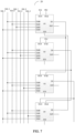
- FIG. 5 another embodiment of the present disclosure further provides a shift register unit 10, and compared with the shift register unit 10 shown in Fig. 4 , the output circuit 300 of the shift register unit 10 shown in Fig. 5 may further include an eighteenth transistor M18, and correspondingly, the noise reduction circuit 500 may further include a nineteenth transistor M19.
- a gate of the eighteenth transistor M18 is coupled to the first node Q, a first electrode of the eighteenth transistor M18 is coupled to a fifth clock signal terminal CLKE to receive a fifth clock signal, and a second electrode of the eighteenth transistor M18 is coupled to another pixel signal output terminal OUT2.
- the eighteenth transistor M18 is turned on, thereby outputting the fifth clock signal to the pixel signal output terminal OUT2.
- the fifth clock signal input by the fifth clock signal terminal CLKE may be configured to be the same as the fourth clock signal input by the fourth clock signal terminal CLKD; for another example, in another example, the fifth clock signal may be different from the fourth clock signal, so that the pixel signal output terminals OUT and OUT2 may output different signals, respectively, to improve the driving capability.
- a gate of the nineteenth transistor M19 is coupled to the second node QB, a first electrode of the nineteenth transistor M19 is coupled to the pixel signal output terminal OUT2, and a second electrode of the nineteenth transistor M19 is coupled to the third voltage terminal VGL2.
- the nineteenth transistor M19 is turned on, so that noise reduction of the pixel signal output terminal OUT2 can be performed using the third voltage terminal VGL 2.
- the potential at the control node H may be maintained by the first capacitor C1, and the potential at the first node Q may be maintained by the second capacitor C2.
- the first capacitor C1 and/or the second capacitor C2 may be implemented by a capacitor device manufactured by a process, for example, by manufacturing dedicated capacitor electrodes, each electrode of the capacitor may be implemented by a metal layer, a semiconductor layer (e.g., doped polysilicon), or the like, or the first capacitor C1 and/or the second capacitor C2 may be implemented by a parasitic capacitor between the devices.
- connection mode of the first capacitor C1 and/or the second capacitor C2 is not limited to the above-described mode, and other suitable connection modes may be used as long as the level written into the control node H or the first node Q can be stored.
- transistors e.g., the first transistor M1, the second transistor M2, the fourth transistor M4, the eleventh transistor M11, the sixteenth transistor M16, and the seventeenth transistor M17 of which first electrodes are coupled to the first node Q and/or the control node H and of which second electrodes each are coupled to a low-level signal terminal.
- the first electrode of the second transistor M2 is coupled to the blanking input signal terminal STU1
- the second electrode of the second transistor M2 is coupled to the control node H.
- a shift register unit 10 capable of preventing current leakage is provided in an embodiment of the present disclosure.
- the shift register unit 10 is different from the shift register unit 10 in Fig. 4 in that a first leakage prevention transistor M1_b, a second leakage prevention transistor M2_b, a fourth leakage prevention transistor M4_b, an eleventh leakage prevention transistor M11_b, a sixteenth leakage prevention transistor M16_b, a seventeenth leakage prevention transistor M17_b, a twentieth transistor M20 and a twenty-first transistor M21 are added.
- the operation principle of the leakage prevention will be described below by taking the second leakage prevention transistor M2_b as an example.
- a gate of the second leakage prevention transistor M2_b is coupled to the second clock signal terminal CLKB, a first electrode of the second leakage prevention transistor M2_b is coupled to a second electrode of the twentieth transistor M20, and a second electrode of the second leakage prevention transistor M2_b is coupled to the control node H.
- a gate of the twentieth transistor M20 is coupled to the control node H, and a first electrode of the twentieth transistor M20 is coupled to the second voltage terminal VDD to receive the second voltage at the high level.
- the twentieth transistor M20 When the control node H is at the high level, the twentieth transistor M20 is turned on under the control of the level of the control node H, so that a high level signal input from the second voltage terminal VDD can be input to the first electrode of the second leakage prevention transistor M2_b, thereby causing both the first electrode and the second electrode of the second leakage prevention transistor M2_b to be in the high level state, preventing the charges at the control node H from leaking through the second leakage prevention transistor M2_b.
- the first leakage prevention transistor M1_b in combination with the twentieth transistor M20 may prevent the charges at the control node H from leaking through the first leakage prevention transistor M1_b and the first transistor M1.
- the fourth leakage prevention transistor M4_b, the eleventh leakage prevention transistor M11_b, the sixteenth leakage prevention transistor M16_b, and the seventeenth leakage prevention transistor M17_b may implement a leakage prevention structure in combination with the twenty-first transistor M21, respectively, so that the leakage of the charge at the first node Q may be prevented.
- the working principle of preventing the first node Q from leaking is the same as the working principle of preventing the control node H from leaking, and the detailed description is omitted here.
- all the transistors used in the embodiments of the present disclosure may be thin film transistors, field effect transistors, or other switching devices with the same characteristics, and all the embodiments of the present disclosure are described by taking thin film transistors as examples.
- the source and the drain of the transistor used herein may be symmetrical in structure, so that there may be no difference in structure between the source and the drain.
- the transistors in order to distinguish two electrodes of a transistor except for the gate, one of them is directly described as the first electrode, and the other is the second electrode. Further, the transistors may be classified into N-type and P-type transistors according to their characteristics.
- the turn-on voltage is a low level voltage (e.g., 0V, -5V, -10V or other suitable voltage), and the turn-off voltage is a high level voltage (e.g., 5V, 10V or other suitable voltage); in a case where the transistor is an N-type transistor, the turn-on voltage is a high level voltage (e.g., 5V, 10V, or other suitable voltage) and the turn-off voltage is a low level voltage (e.g., 0V, -5V, -10V, or other suitable voltage).
- the transistors used in the shift register unit 10 provided in the embodiments of the present disclosure are all illustrated by taking N-type transistors as examples, the embodiments of the present disclosure include but are not limited to this, for example, at least some of the transistors in the shift register unit 10 may also be P-type transistors.
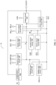
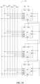
- an embodiment of the present disclosure provides a gate driving circuit 20, as shown in Fig. 7 , the gate driving circuit 20 includes a plurality of shift register units 10 which are cascaded, where any one or more shift register units 10 may adopt the structure of the shift register unit 10 provided in the embodiments of the present disclosure or a variation thereof. Note that only the front four stages of shift register units (A1, A2, A3, and A4) of the gate driving circuit 20 are schematically shown in Fig. 7 .
- the gate driving circuit 20 further includes a first sub-clock signal line CLK_1, a second sub-clock signal line CLK_2, a third sub-clock signal line CLK_3, and a fourth sub-clock signal line CLK_4.
- the shift register unit includes the fourth clock signal terminal CLK_D
- the fourth clock signal terminal CLKD of the shift register unit of the (4n-3) th stage is coupled to the first sub-clock signal line CLK_1
- the fourth clock signal terminal CLKD of the shift register unit of the (4n-2) th stage is coupled to the second sub-clock signal line CLK_2
- the fourth clock signal terminal CLKD of the shift register unit of the (4n-1) th stage is coupled to the third sub-clock signal line CLK_3
- the fourth clock signal terminal CLKD of the shift register unit of the (4n) th stage is coupled to the fourth sub-clock signal line CLK_4, where n is an integer greater than 0.
- the gate driving circuit 20 may further include a fifth sub-clock signal line CLK_5 and a sixth sub-clock signal line CLK_6.
- the shift register unit includes the second clock signal terminal CLKB and the third clock signal terminal CLKC
- the second clock signal terminal CLKB of the shift register unit of the (2n-1) th stage is coupled to the fifth sub-clock signal line CLK_5, and the third clock signal terminal CLKC is coupled to the sixth sub-clock signal line CLK_6
- the second clock signal terminal CLKB of the shift register unit of the (2n) th stage is coupled to the sixth sub-clock signal line CLK_6,
- the third clock signal terminal CLKC is coupled to the fifth sub-clock signal line CLK_5, where n is an integer greater than 0.
- the gate driving circuit 20 may further include a seventh sub-clock signal line CLK_7, and the first clock signal terminal CLKA of each stage of the shift register unit is coupled to the seventh sub-clock signal line CLK_7.
- the blanking input signal terminal STU1 and the display input signal terminal STU2 of the shift register unit of the first stage, and the display input signal terminal STU2 of the shift register unit of the second stage are coupled to the input signal line STU, for example, to receive a trigger signal STV.
- the blanking input signal terminal STU1 of the shift register unit of the (n+1) th stage, except for the shift register unit of the first stage, is coupled with the shift signal output terminal CR of the shift register unit of the n th stage.
- the display input signal terminal STU2 of the shift register unit of the (n+2) th stage is coupled to the shift signal output terminal CR of the shift register unit of the n th stage.
- the display reset signal terminal STD of the shift register unit of the n th stage is coupled to the shift signal output terminal CR of the shift register unit of the (n+3) th stage, where n is an integer greater than 0.
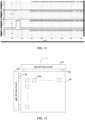
- Fig. 8 shows a signal timing chart illustrating signals of the gate driving circuit 20 shown in Fig. 7 when used for the progressive sequential compensation
- Fig. 9 shows a signal timing chart illustrating signals of the gate driving circuit 20 shown in Fig. 7 when used for the random compensation.
- Q ⁇ 1> and Q ⁇ 2> respectively denote the first nodes Q in the shift register units of the first stage and the second stage in the gate driving circuit 20.
- OUT ⁇ 1>, OUT ⁇ 2>, OUT ⁇ 3>, and OUT ⁇ 4> respectively denote pixel signal output terminals OUT of the shift register units of the first stage, the second stage, the third stage, and the fourth stage in the gate driving circuit 20.
- 1F, 2F, 3F, and 4F denote a first frame, a second frame, a third frame, and a fourth frame, respectively.
- Display denotes a display period of the frame
- Blank denotes a blanking period of the frame.
- a DC low-level signal is input through the compensation selection control terminal OE, so that the first transistor M1 remains turned off.
- the fifth and sixth sub-clock signal lines CLK_5 and CLK_6 are supplied with a high level, and since the fifth and sixth sub-clock signal lines CLK_5 and CLK_6 are alternately coupled to the second clock signal terminal CLKB of the shift register unit, the second transistor M2 and the sixteenth transistor M16 of the shift register unit of each stage may be turned on, and thus the control node H and the first node Q of the shift register unit of each stage may be reset to implement global reset. Then, the signal supplied from the sixth sub-clock signal line CLK_6 becomes a low level, and the signal supplied from the fifth sub-clock signal line CLK_5 continues to remain the high level.
- the ninth transistor M9 Since a high level is input from the fifth voltage terminal VDD_B, the ninth transistor M9 is turned on, so that the second node QB is charged to the high level. The high level of the second node QB turns on the eleventh transistor M11, thereby pulling down the first node Q to the low level.
- the blanking input signal terminal STU1 and the display input signal terminal STU2 of the shift register unit of the first stage are both coupled to the input signal line STU, so that the blanking input signal terminal STU1 and the display input signal terminal STU2 are both initially input with a high level, and at the same time, since the second clock signal terminal CLKB (coupled to the fifth sub-clock signal line CLK_5) is input with a high level, the second transistor M2 is turned on, and the control node H is charged to a high level, which is then stored by the first capacitor C1.
- the fifteenth transistor M15 is turned on by the high level of the display input signal terminal STU2, so that the second node QB may be secondarily pulled down.
- the second clock signal terminal CLKB is input with a low level
- the second transistor M2 is turned off, and the display input signal terminal STU2 continues to be input with the high level, so that the high level signal of the second voltage terminal VDD can charge the first node Q through the fifth transistor M5, and the first node Q is pulled up to the high level, which is then stored by the second capacitor C2.
- the sixth transistor M6 and the seventh transistor M7 are turned on under the control of the first node Q, but since the fourth clock signal terminal CLKD (coupled to the first sub-clock signal line CLK_1) is input with a low level signal at this time, both the shift signal output terminal CR and the pixel signal output terminal OUT each output a low level signal.
- the fourth clock signal terminal CLKD is input with a high level signal
- the potential of the first node Q is further pulled up due to the bootstrap effect, so the sixth transistor M6 and the seventh transistor M7 remain turned on, and thus both the shift signal output terminal CR and the pixel signal output terminal OUT each output a high level signal.
- the high level signal output from the shift signal output terminal CR may be used for scan shift from a shift register unit of a previous stage to that of a next stage
- the high level signal output from the pixel signal output terminal OUT may be used for driving the sub-pixel units in the display panel to perform display.
- a low level signal is then input to the fourth clock signal terminal CLKD, and both the shift signal output terminal CR and the pixel signal output terminal OUT can be discharged through the fourth clock signal terminal CLKD, thereby completing the reset of the shift signal output terminal CR and the pixel signal output terminal OUT.
- the shift signal output terminal CR and the pixel signal output terminal OUT are reset to the low level, the potential of the first node Q is lowered by an amplitude with the coupling action between the transistors; meanwhile, the display reset signal terminal STD of the shift register unit of the first stage is coupled with the shift signal output terminal CR of the shift register unit of the fourth stage, and at this time, the shift signal output terminal CR of the shift register unit of the fourth stage does not output a high level signal, so that the first node Q is not pulled down, and the first node Q can be kept at a relatively high level.
- the shift signal output terminal CR of the shift register unit of the fourth stage then outputs a high level, so that the display reset signal terminal STD of the shift register unit of the first stage is input with a high level signal, the seventeenth transistor M17 is turned on, and the first node Q is pulled down to the low level, completing the reset of the first node Q.
- the potential change of the first node Q of the first stage takes on a "tower shape".
- the shift signal output terminal CR and the pixel signal output terminal OUT are at the high level, the potential of the first node Q rises due to the bootstrap effect, so that when the shift signal output terminal CR and the pixel signal output terminal OUT are discharged through the sixth transistor M6 and the seventh transistor M7, respectively, the current flowing through the transistors may be greater, and the discharge speed is faster.
- the twelfth transistor M12 and the thirteenth transistor M13 for resetting can be transistors with smaller sizes, so that the layout area occupied by the shift register unit can be reduced.
- the fourth transistor M4 is kept in the off state, and the fourth transistor M4 isolates the influence of the high level pre-stored at the control node H on the display period.
- the shift register unit of the first stage drives the sub-pixels in the first row in the display panel to complete display
- the shift register unit of the second stage, the shift register unit of the third stage and the like drive the sub-pixel units in the display panel row by row to complete display driving of the frame.
- the display period of the first frame ends.
- the control node H maintains the high level of the display period due to the storage of the first capacitor C1, the first clock signal terminal CLKA (coupled to the seventh sub-clock signal line CLK_7) and the third clock signal terminal CLKC (coupled to the sixth sub-clock signal line CLK_6) are input with the high level signal at the beginning, the third transistor M3 and the fourth transistor M4 are turned on, so that the high level of the third clock signal terminal CLKC may charge the first node Q, pulling the first node Q up to the high level.
- the tenth transistor M10 is turned on under the control of the first node Q, the second node QB is pulled down to the low level, and the fourteenth transistor M14 is also turned on under the control of the first clock signal terminal CLKA, which may further pull down the second node QB.
- the first clock signal terminal CLKA is input with a low level signal, and the fourth transistor M4 is turned off.
- the fourth clock signal terminal CLKD (coupled to the first sub-clock signal line CLK_1) is input with a high level signal, the potential of the first node Q is further pulled up due to the bootstrap effect, the sixth transistor M6 and the seventh transistor M7 are turned on, and the high level signal input from the fourth clock signal terminal CLKD may be output to the shift signal output terminal CR and the pixel signal output terminal OUT.
- the signal output by the pixel signal output terminal OUT can be used to drive a sensing transistor in a sub-pixel unit in the display panel to achieve external compensation.
- the second transistor M2 in the shift register unit of the second stage is turned on, so that the control node H ⁇ 2> in the shift register unit of the second stage is pulled up to a high level.
- a seventh stage 7 after the control node H ⁇ 2> in the shift register unit of the second stage is sufficiently written with the high level, the sixth sub-clock signal line CLK_6 is input with the low level signal. Meanwhile, the fourth clock signal terminal CLKD is continuously input with the high level, so the shift signal output terminal CR and the pixel signal output terminal OUT of the shift register unit of the first stage keep outputting the high level signal. In this process, the fourth transistor M4 is kept in the off state all the time, so that the first node Q ⁇ 1> can be prevented from leaking through the fourth transistor M4.
- the fifth sub-clock signal line CLK_5 is input with a high level signal, and since the second clock signal terminals CLKB of the shift register units of the odd-numbered stages are all coupled to the fifth sub-clock signal line CLK_5, the reset of the control nodes H and the first nodes Q in all the shift register units of the odd-numbered stages, particularly the reset of the first nodes Q of the first and third stages and the control node H of the first stage, can be completed.
- the threshold voltage of the transistor may be positively drifted when a positive voltage is applied to the transistor, the time for which the control node H needs to be kept at the positive voltage can be shortened by the above manner, so that the time for the threshold voltage of the transistor to be positively drifted is shortened, and the reliability of the transistor is improved.
- the gate driving circuit 20 repeats the same operation as the display period of the first frame, and is not described here again.
- the first clock signal terminal CLKA and the third clock signal terminal CLKC of the shift register unit of the second stage each are input with a high level signal, and the third transistor M3 and the fourth transistor M4 are turned on, so that the high level input by the third clock signal terminal CLKC can charge the first node Q, pulling up the first node Q to a high level.
- the shift signal output terminal CR and the pixel signal output terminal OUT output high level signals while charging the control node H in the shift register unit of the third stage.
- a high level signal is input by the sixth sub-clock signal line CLK_6, and since the second clock signal terminals CLKB of the shift register units of the even-numbered stages are all coupled to the sixth sub-clock signal line CLK_6, the reset of the control nodes H and the first nodes Q in all the shift register units of the even-numbered stages can be completed.
- the gate driving circuit outputs the driving signals for the sensing transistors in the sub-pixel units in the display panel in the blanking period of each frame, and the driving signals are sequentially supplied row by row. For example, in the blanking period of the first frame, the gate driving circuit outputs the driving signal for the sub-pixel units of the first row in the display panel, in the blanking period of the second frame, the gate driving circuit outputs the driving signal for the sub-pixel units of the second row in the display panel, and so on, the progressive sequential compensation is completed.
- the shift register unit shown in Fig. 4 may be used as the shift register unit in the gate driving circuit 20 shown in Fig. 7 .
- the operation principle of the gate driving circuit is similar to that in the above-described progressive sequential compensation, and only the difference is described below.
- the compensation selection control terminal OE is also supplied with a high level signal, at which time the control node H ⁇ 1> of the shift register unit of the first stage is charged to a high level, and then the control node H ⁇ 2> of the shift register unit of the second stage is also charged to a high level because the output pulses of OUT ⁇ 1> and OUT ⁇ 2> overlap.
- the control node H ⁇ 1> of the shift register unit of the first stage and the control node H ⁇ 2> of the shift register unit of the second stage are both charged to the high level, but in the blanking period of the first frame, for example, when it is necessary to output a driving signal for detecting the first row of sub-pixel units in the display panel in the frame, the following operation is performed in the blanking period of the first frame.
- a high level signal is input by the sixth sub-clock signal line CLK_6, thereby discharging the control nodes H of shift register units of the even-numbered stages, that is, eliminating the high level of H ⁇ 2> (for example, eliminating the high levels of the control nodes H of the shift register units of the (n-1) th and the (n+1) th stages, if the shift register unit of the n th stage needs to be detected in the frame).
- the seventh sub-clock signal line CLK_7 (coupled to the first clock signal terminal CLKA) is input with a high level signal
- the third clock signal terminal CLKC of the shift register unit of the first stage maintains to be input with the high level signal
- the third transistor M3 and the fourth transistor M4 are turned on, and the charging of the first node Q is completed.
- a third stage T3 low-level signals are input by the sixth and seventh sub-clock signal lines CLK_6 and CLK_7, and a high level signal is input by the first sub-clock signal line CLK_1, so the shift signal output terminal and the pixel signal output terminal OUT output high level signals.
- the signal output by the pixel signal output terminal OUT can be used to drive the sensing transistor in the sub-pixel units of the first row in the display panel for external compensation.
- the signal of the first sub-clock signal line CLK_1 becomes a low level signal, and accordingly, the shift signal output terminal and the pixel signal output terminal OUT output low level signals.
- a high level signal is input by the fifth sub-clock signal line CLK_5, and since the second clock signal terminals CLKB of the shift register units of the odd-numbered stages are all coupled to the fifth sub-clock signal line CLK_5, the reset of the control nodes H and the first nodes Q in all the shift register units of the odd-numbered stages, and particularly the reset of the first node Q and the control node H of the shift register unit of the first stage, can be completed.
- the signal input by the compensation selection control terminal OE is made to be the same as the signal outputted by the pixel signal output terminal OUT ⁇ 2> (i.e., the shift signal output terminal CR) of the shift register unit of the second stage, and the control nodes H ⁇ 1>, H ⁇ 2> and H ⁇ 3> of the shift register units of the first stage, the second stage and the third stage are all charged to a high level under the control of the compensation selection control terminal OE due to the overlap of output pulses of the pixel signal output terminals OUT ⁇ 2>, OUT ⁇ 1> and OUT ⁇ 3> (not shown in Fig. 9 ) of the shift register units of the first to third stages.
- the control node H ⁇ 1> is charged to the high level and then pulled down fast by the low level of the shift signal output terminal CR (i.e., the pixel signal output terminal OUT ⁇ 1 >).
- the description is given by taking as an example that the driving signal corresponding to the first row of the sub-pixel units of the display panel is output in the blanking period of the first frame, and the disclosure is not limited thereto.
- the timing simulation diagram shown in Fig. 11 when it is necessary to output a driving signal corresponding to the fifth row of sub-pixel units of the display panel in the blanking period of a certain frame, it is necessary to control so that the timings of the signals supplied to the compensation selection control terminal OE and the signal output terminal CR ⁇ 5> of the shift register unit of the fifth stage are the same.
- CR ⁇ 4> and CR ⁇ 6> in Fig. 11 denote a shift signal output terminal of the shift register unit of the fourth stage and a shift signal output terminal of the shift register unit of the sixth stage, respectively.
- the compensation selection circuit 400 (the first transistor M1), when it is necessary to output the driving signal corresponding to the sub-pixel units of the n th row of the display panel in the blanking period of a certain frame, it is necessary to make the signal supplied to the compensation selection control terminal OE and the signal of the shift signal output terminal CR of the shift register unit of the n th stage have a same timing, whereby the random compensation can be achieved, where n is an integer greater than 0.
- another embodiment of the present disclosure further provides a gate driving circuit 20, the differences between the present gate driving circuit 20 and the gate driving circuit 20 shown in Fig. 7 include: the blanking input signal terminal STU1 and the display input signal terminal STU2 of the shift register unit of the (n+1) th stage, except for the shift register unit of the first stage, are coupled to the shift signal output terminal CR of the shift register unit of the n th stage; the display reset signal terminal STD of the shift register unit of the n th stage, except for the shift register unit of the last stage, is coupled to the shift signal output terminal CR of the shift register unit of the (n+1) th stage.
- the blanking input signal terminal STU1 and the display input signal terminal STU2 of the shift register unit of the (n+1) th stage except for the shift register unit of the first stage, are coupled to the shift signal output terminal CR of the shift register unit of the n th stage
- the display reset signal terminal STD of the shift register unit of the n th stage except for the shift register unit
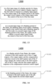
- An embodiment of the present disclosure also provides a display device 1, as shown in Fig. 12 , the display device 1 includes the gate driving circuit 20 provided by the embodiments of the present disclosure.
- the display device 1 further includes a display panel 40, which includes a plurality of sub-pixel units 410 in an array.
- the display device 1 may further include a data driving circuit 30.
- the data driving circuit 30 is used for supplying data signals to the pixel array.
- the gate drive circuit 20 is used to provide driving signals to the pixel array, for example, the driving signals may drive scan transistors and sense transistors in the sub-pixel units 410.
- the data driving circuit 30 is electrically coupled to the sub-pixel units 410 through data lines DL, and the gate driving circuit 20 is electrically coupled to the sub-pixel units 410 through gate lines GL.
- the display device 1 in the present embodiment may be any product or component with a display function, such as a liquid crystal panel, a liquid crystal television, a display, an OLED panel, an OLED television, an electronic paper display device, a mobile phone, a tablet computer, a notebook computer, a digital photo frame, a navigator and the like.
- a display function such as a liquid crystal panel, a liquid crystal television, a display, an OLED panel, an OLED television, an electronic paper display device, a mobile phone, a tablet computer, a notebook computer, a digital photo frame, a navigator and the like.
- Embodiments of the present disclosure also provide a driving method 1300, which may be used to drive the shift register unit 10 provided by the embodiments of the present disclosure, where the driving method 1300 includes the following steps.
- the display input circuit 200 inputs a display signal to the first node Q in response to a display input signal; in a first output stage of the display period of the frame, the output circuit 300 outputs a first output signal under the control of the level of the first node Q.
- the first output signal may be used to drive the sub-pixel units in the display panel to display.
- the blanking input circuit 100 inputs a blanking input signal to the control node H and a blanking signal to the first node Q; in a second output stage of the blanking period of the frame, the output circuit 300 outputs a second output signal under the control of the level of the first node Q.
- the second output signal may be used to drive the sub-pixel units in the display panel to perform external compensation.
- the composite output signal includes a first output signal and a second output signal.
- the driving method 1300 may further include: the compensation selection circuit 400 charges the control node with the first output signal in response to the compensation selection control signal during the display period of the frame.
- Embodiments of the present disclosure also provide a driving method 1400, which may be used to drive the gate driving circuit 20 provided by the embodiments of the present disclosure, and the driving method includes the following steps.
- step S1402 when the gate driving circuit 20 drives a display panel, in a display period of any frame, the output terminal of the shift register unit 10 of the n th stage outputs a first output signal, and the compensation selection circuit 400 in the shift register unit 10 of the n th stage charges the control node H in the shift register unit 10 of the n th stage with the first output signal in response to the compensation selection control signal.
- the output terminal of the shift register unit of the n th stage outputs the second output signal.
- the composite output signal includes a first output signal and the second output signal, where n is an integer greater than 0.
Landscapes
- Engineering & Computer Science (AREA)
- Physics & Mathematics (AREA)
- Computer Hardware Design (AREA)
- General Physics & Mathematics (AREA)
- Theoretical Computer Science (AREA)
- Control Of Indicators Other Than Cathode Ray Tubes (AREA)
- Shift Register Type Memory (AREA)
- Devices For Indicating Variable Information By Combining Individual Elements (AREA)
- Control Of El Displays (AREA)
- Liquid Crystal Display Device Control (AREA)
Claims (11)
- Schieberegistereinheit (10), eine Austasteingangsschaltung (100), eine Anzeigeeingangsschaltung (200), eine Ausgangsschaltung (300) und eine Kompensationsauswahlschaltung (400) aufweisend, wobeidie Austasteingangsschaltung (100) konfiguriert ist, um während einer Austastperiode eines Rahmens ein Austasteingangssignal an einen Steuerknoten (H) einzugeben und ein Austastsignal an einen ersten Knoten (Q) einzugeben;die Anzeigeeingangsschaltung (200) konfiguriert ist, um in einer Anzeigeperiode des Rahmens als Reaktion auf ein Anzeigeeingangssignal ein Anzeigesignal an den ersten Knoten (Q) einzugeben;die Ausgangsschaltung (300) konfiguriert ist, um ein zusammengesetztes Ausgangssignal an einen Ausgangsanschluss (OUTPUT) unter der Steuerung eines Pegels des ersten Knotens (Q) auszugeben; unddie Kompensationsauswahlschaltung (400) elektrisch mit dem Ausgangsanschluss (OUTPUT) gekoppelt ist und konfiguriert ist, um den Steuerknoten (H) mit dem zusammengesetzten Ausgangssignal als Reaktion auf ein Kompensationsauswahlsteuersignal zu laden, wobei das zusammengesetzte Ausgangssignal ein erstes Ausgangssignal und ein zweites Ausgangssignal aufweist,die Ausgangsschaltung (300) konfiguriert ist, um in der Anzeigeperiode des Rahmens das erste Ausgangssignal unter der Steuerung des Pegels des ersten Knotens (Q) an den Ausgangsanschluss (OUTPUT) auszugeben; unddie Ausgangsschaltung (300) konfiguriert ist, um in der Austastperiode des Rahmens das zweite Ausgangssignal an den Ausgangsanschluss (OUTPUT) unter der Steuerung des Pegels des ersten Knotens (Q) auszugeben,die Kompensationsauswahlschaltung (400) konfiguriert ist, um in der Anzeigeperiode des Rahmens als Reaktion auf das Kompensationsauswahlsteuersignal den Steuerknoten (H) mit dem ersten Ausgangssignal zu laden, undwobei der Ausgangsanschluss (OUTPUT) einen Schiebesignalausgangsanschluss (CR) aufweist, der Schiebesignalausgangsanschluss (CR) das zusammengesetzte Ausgangssignal ausgibt und die Kompensationsauswahlschaltung (400) einen ersten Transistor (M1) aufweist;ein Gate des ersten Transistors (M1) mit einem Kompensationsauswahlsteueranschluss gekoppelt ist, um das Kompensationsauswahlsteuersignal zu empfangen, eine erste Elektrode des ersten Transistors (M1) mit dem Schiebesignalausgangsanschluss (CR) gekoppelt ist, um das zusammengesetzte Ausgangssignal zu empfangen, und eine zweite Elektrode des ersten Transistors (M1) mit dem Steuerknoten (H) gekoppelt ist, undwobei die Austasteingangsschaltung (100) aufweist:eine Lade-Teilschaltung (110), die konfiguriert ist, um das Austasteingangssignal als Reaktion auf ein zweites Taktsignal in den Steuerknoten (H) einzugeben;eine Speicher-Teilschaltung (120), die konfiguriert ist, um das Austasteingangssignal, das von der Lade-Teilschaltung (110) eingegeben ist, zu speichern; undeine Isolations-Teilschaltung (130), die konfiguriert ist, um das Austastsignal unter der Steuerung eines Pegels des Steuerknotens (H) und eines ersten Taktsignals in den ersten Knoten (Q) einzugeben, und wobeidie Lade-Teilschaltung (110) einen zweiten Transistor (M2) aufweist, ein Gate des zweiten Transistors (M2) mit einem zweiten Taktsignalanschluss (CLKB) gekoppelt ist, um das zweite Taktsignal zu empfangen, eine erste Elektrode des zweiten Transistors (M2) mit einem Austasteingangssignalanschluss (STU1) gekoppelt ist, um das Austasteingangssignal zu empfangen, und eine zweite Elektrode des zweiten Transistors (M2) mit dem Steuerknoten (H) gekoppelt ist;die Speicher-Teilschaltung (120) einen ersten Kondensator (C1) aufweist, eine erste Elektrode des ersten Kondensators (C1) mit dem Steuerknoten (H) gekoppelt ist und eine zweite Elektrode des ersten Kondensators (C1) mit einem ersten Spannungsanschluss (VGL1) gekoppelt ist, um eine erste Spannung zu empfangen;die Isolations-Teilschaltung (130) einen dritten Transistor (M3) und einen vierten Transistor (M4) aufweist, ein Gate des dritten Transistors (M3) mit dem Steuerknoten (H) gekoppelt ist, eine erste Elektrode des dritten Transistors (M3) mit einem dritten Taktsignalanschluss (CLKC) gekoppelt ist, um ein drittes Taktsignal als Austastsignal zu empfangen, eine zweite Elektrode des dritten Transistors (M3) mit einer ersten Elektrode des vierten Transistors (M4) gekoppelt ist, ein Gate des vierten Transistors (M4) mit dem ersten Taktsignalanschluss (CLKA) gekoppelt ist, um das erste Taktsignal zu empfangen, und eine zweite Elektrode des vierten Transistors (M4) mit dem ersten Knoten (Q) gekoppelt ist, undwobei die Anzeigeeingangsschaltung (200) einen fünften Transistor (M5) aufweist;ein Gate des fünften Transistors (M5) mit einem Anzeigeeingangssignalanschluss (STU2) gekoppelt ist, um das Anzeigeeingangssignal zu empfangen, eine erste Elektrode des fünften Transistors (M5) mit einem zweiten Spannungsanschluss (VDD) gekoppelt ist, um eine zweite Spannung als das Anzeigesignal zu empfangen, und eine zweite Elektrode des fünften Transistors (M5) mit dem ersten Knoten (Q) gekoppelt ist, wobei der Ausgangsanschluss (OUTPUT) ferner einen Pixelsignalausgangsanschluss (OUT2) aufweist, der Pixelsignalausgangsanschluss (OUT2) das zusammengesetzte Ausgangssignal ausgibt und die Ausgangsschaltung (300) einen sechsten Transistor (M6), einen siebten Transistor (M7) und einen zweiten Kondensator (C2) aufweist;ein Gate des sechsten Transistors (M6) mit dem ersten Knoten (Q) gekoppelt ist, eine erste Elektrode des sechsten Transistors (M6) mit einem vierten Taktsignalanschluss (CLKD) gekoppelt ist, um ein viertes Taktsignal als das zusammengesetzte Ausgangssignal zu empfangen, und eine zweite Elektrode des sechsten Transistors (M6) mit dem Schiebesignalausgangsanschluss (CR) gekoppelt ist;ein Gate des siebten Transistors (M7) mit dem ersten Knoten (Q) gekoppelt ist, eine erste Elektrode des siebten Transistors (M7) mit dem vierten Taktsignalanschluss (CLKD) gekoppelt ist, um das vierte Taktsignal als zusammengesetztes Ausgangssignal zu empfangen, und eine zweite Elektrode des siebten Transistors (M7) mit dem Pixelsignalausgangsanschluss (OUT2) gekoppelt ist;eine erste Elektrode des zweiten Kondensators (C2) mit dem ersten Knoten (Q) gekoppelt ist und eine zweite Elektrode des zweiten Kondensators (C2) mit der zweiten Elektrode des sechsten Transistors (M6) gekoppelt ist.
- Schieberegistereinheit nach Anspruch 1, ferner eine Rauschunterdrückungsschaltung und eine erste Steuerschaltung (600) aufweisend, wobeidie erste Steuerschaltung (600) konfiguriert ist, um einen Pegel eines zweiten Knotens unter der Steuerung des Pegels des ersten Knotens (Q) zu steuern; unddie Rauschunterdrückungsschaltung konfiguriert ist, um ein Rauschen des ersten Knotens (Q), des Schiebesignalausgangsanschlusses (CR) und des Pixelsignalausgangsanschlusses (OUT2) unter der Steuerung des Pegels des zweiten Knotens zu reduzieren.
- Schieberegistereinheit nach Anspruch 2, wobei die erste Steuerschaltung (600) einen achten Transistor (M8), einen neunten Transistor (M9) und einen zehnten Transistor (M10) aufweist;ein Gate und eine erste Elektrode des achten Transistors (M8) miteinander gekoppelt sind und konfiguriert sind, um mit einem vierten Spannungsanschluss (VDD_A) gekoppelt zu werden, um eine vierte Spannung zu empfangen, und eine zweite Elektrode des achten Transistors (M8) mit dem zweiten Knoten gekoppelt ist;ein Gate und eine erste Elektrode des neunten Transistors (M9) miteinander gekoppelt sind und konfiguriert sind, um mit einem fünften Spannungsanschluss gekoppelt zu werden, um eine fünfte Spannung zu empfangen, und eine zweite Elektrode des neunten Transistors (M9) mit dem zweiten Knoten gekoppelt ist; undein Gate des zehnten Transistors (M10) mit dem ersten Knoten (Q) gekoppelt ist, eine erste Elektrode des zehnten Transistors (M10) mit dem zweiten Knoten gekoppelt ist und eine zweite Elektrode des zehnten Transistors (M10) mit einem ersten Spannungsanschluss (VGL1) gekoppelt ist, um eine erste Spannung zu empfangen, undwobei die Rauschunterdrückungsschaltung einen elften Transistor (M11), einen zwölften Transistor (M12) und einen dreizehnten Transistor (M13) aufweist;ein Gate des elften Transistors (M11) mit dem zweiten Knoten gekoppelt ist, eine erste Elektrode des elften Transistors (M11) mit dem ersten Knoten (Q) gekoppelt ist und eine zweite Elektrode des elften Transistors (M11) mit einem ersten Spannungsanschluss (VGL1) gekoppelt ist, um eine erste Spannung zu empfangen;ein Gate des zwölften Transistors (M12) mit dem zweiten Knoten gekoppelt ist, eine erste Elektrode des zwölften Transistors (M12) mit dem Schiebesignalausgangsanschluss (CR) gekoppelt ist und eine zweite Elektrode des zwölften Transistors (M12) mit dem ersten Spannungsanschluss (VGL1) gekoppelt ist, um die erste Spannung zu empfangen; undein Gate des dreizehnten Transistors (M13) mit dem zweiten Knoten gekoppelt ist, eine erste Elektrode des dreizehnten Transistors (M13) mit dem Pixelsignalausgangsanschluss (OUT2) gekoppelt ist und eine zweite Elektrode des dreizehnten Transistors (M13) mit einem dritten Spannungsanschluss (VGL2) gekoppelt ist, um eine dritte Spannung zu empfangen.
- Schieberegistereinheit nach Anspruch 2, ferner eine zweite Steuerschaltung (700) aufweisend, wobeidie zweite Steuerschaltung (700) konfiguriert ist, um den Pegel des zweiten Knotens als Reaktion auf ein Austaststeuersignal zu steuern, undwobei die zweite Steuerschaltung (700) einen vierzehnten Transistor (M14) aufweist und das Austaststeuersignal ein erstes Taktsignal aufweist;ein Gate des vierzehnten Transistors (M14) mit einem ersten Taktsignalanschluss (CLKA) gekoppelt ist, um das erste Taktsignal zu empfangen, eine erste Elektrode des vierzehnten Transistors (M14) mit dem zweiten Knoten gekoppelt ist und eine zweite Elektrode des vierzehnten Transistors (M14) mit einem ersten Spannungsanschluss (VGL1) gekoppelt ist, um eine erste Spannung zu empfangen, oderdie Schieberegistereinheit ferner eine dritte Steuerschaltung (800) aufweist, wobeidie dritte Steuerschaltung (800) konfiguriert ist, um den Pegel des zweiten Knotens als Reaktion auf ein Anzeigesteuersignal zu steuern, undwobei die dritte Steuerschaltung (800) einen fünfzehnten Transistor (M15) aufweist und das Anzeigesteuersignal das Anzeigeeingangssignal aufweist; undein Gate des fünfzehnten Transistors (M15) mit einem Anzeigeeingangssignalanschluss (STU2) gekoppelt ist, um das Anzeigeeingangssignal zu empfangen, eine erste Elektrode des fünfzehnten Transistors (M15) mit dem zweiten Knoten gekoppelt ist und eine zweite Elektrode des fünfzehnten Transistors (M15) mit einem ersten Spannungsanschluss (VGL1) gekoppelt ist, um eine erste Spannung zu empfangen.
- Schieberegistereinheit nach einem der Ansprüche 1 und 2 bis 4, ferner eine Austastrücksetzschaltung (900) aufweisend, wobei die Austastrücksetzschaltung (900) konfiguriert ist, um den ersten Knoten (Q) als Reaktion auf ein Austastrücksetzsignal zurückzusetzen, undwobei die Austastrücksetzschaltung (900) einen sechzehnten Transistor (M16) aufweist; undein Gate des sechzehnten Transistors (M16) mit einem zweiten Taktsignalanschluss (CLKB) gekoppelt ist, um ein zweites Taktsignal als das Austastrücksetzsignal zu empfangen, eine erste Elektrode des sechzehnten Transistors (M16) mit dem ersten Knoten (Q) gekoppelt ist und eine zweite Elektrode des sechzehnten Transistors (M16) mit dem ersten Spannungsanschluss (VGL1) gekoppelt ist, um die erste Spannung zu empfangen.
- Schieberegistereinheit nach einem der Ansprüche 1 bis 2, ferner eine Anzeigerücksetzschaltung (1000) aufweisend, wobei die Anzeigerücksetzschaltung (1000) konfiguriert ist, um den ersten Knoten (Q) als Reaktion auf ein Anzeigerücksetzsignal zurückzusetzen, undwobei die Anzeigerücksetzschaltung (1000) einen siebzehnten Transistor (M17) aufweist;ein Gate des siebzehnten Transistors (M17) mit einem Anzeigerücksetzsignalanschluss gekoppelt ist, um das Anzeigerücksetzsignal zu empfangen, eine erste Elektrode des siebzehnten Transistors (M17) mit dem ersten Knoten (Q) gekoppelt ist und eine zweite Elektrode des siebzehnten Transistors (M17) mit einem ersten Spannungsanschluss (VGL1) gekoppelt ist, um eine erste Spannung zu empfangen.
- Gate-Ansteuerschaltung (20), mehrere Schieberegistereinheiten aufweisend, die kaskadiert sind, wobei jede der Schieberegistereinheiten die Schieberegistereinheit (10) nach einem der Ansprüche 1 bis 6 ist.
- Gate-Ansteuerschaltung nach Anspruch 7, ferner eine erste Sub-Taktsignalleitung (CLK_1), eine zweite Sub-Taktsignalleitung (CLK_2), eine dritte Sub-Taktsignalleitung (CLK_3) und eine vierte Sub-Taktsignalleitung (CLK_4) aufweisend, wobei die Schieberegistereinheit (10) einen vierten Taktsignalanschluss aufweist,der vierte Taktsignalanschluss (CLKD) der Schieberegistereinheit der (4n-3)-ten Stufe mit der ersten Sub-Taktsignalleitung (CLK_1) gekoppelt ist;der vierte Taktsignalanschluss (CLKD) der Schieberegistereinheit der (4n-2)-ten Stufe mit der zweiten Sub-Taktsignalleitung (CLK_2) gekoppelt ist;der vierte Taktsignalanschluss (CLKD) der Schieberegistereinheit der (4n-1)-ten Stufe mit der dritten Sub-Taktsignalleitung (CLK_3) gekoppelt ist; undder vierte Taktsignalanschluss (CLKD) der Schieberegistereinheit der (4n)-ten Stufe mit der vierten Sub-Taktsignalleitung (CLK_4) gekoppelt ist;wobei n eine ganze Zahl größer als 0 ist, undwobei die Gate-Ansteuerschaltung (20) ferner eine fünfte Sub-Taktsignalleitung (CLK_5) und eine sechste Sub-Taktsignalleitung (CLK_6) aufweist, wobei die Schieberegistereinheit einen zweiten Taktsignalanschluss (CLKB) und einen dritten Taktsignalanschluss (CLKC) aufweist,der zweite Taktsignalanschluss (CLKB) der Schieberegistereinheit der (2n-1)-ten Stufe mit der fünften Sub-Taktsignalleitung (CLK_5) gekoppelt ist und der dritte Taktsignalanschluss (CLKC) der Schieberegistereinheit der (2n-1)-ten Stufe mit der sechsten Sub-Taktsignalleitung (CLK_6) gekoppelt ist;der zweite Taktsignalanschluss (CLKB) der Schieberegistereinheit der (2n)-ten Stufe mit der sechsten Sub-Taktsignalleitung (CLK_6) gekoppelt ist und der dritte Taktsignalanschluss (CLKC) der Schieberegistereinheit der (2n)-ten Stufe mit der fünften Sub-Taktsignalleitung (CLK_5) gekoppelt ist,wobei n eine ganze Zahl größer als 0 ist.
- Gate-Ansteuerschaltung nach Anspruch 8, wobei die Schieberegistereinheit (10) einen Austasteingangssignalanschluss (STU1), einen Anzeigeeingangssignalanschluss (STU2) und einen Schiebesignalausgangsanschluss (CR) aufweist,der Austasteingangssignalanschluss (STU1) der Schieberegistereinheit der (n+1)-ten Stufe mit dem Schiebesignalausgangsanschluss (CR) der Schieberegistereinheit der n-ten Stufe gekoppelt ist;der Anzeigeeingangssignalanschluss (STU2) der Schieberegistereinheit der (n+2)-ten Stufe mit dem Schiebesignalausgangsanschluss (CR) der Schieberegistereinheit der n-ten Stufe gekoppelt ist;wobei n eine ganze Zahl größer als 0 ist.
- Anzeigevorrichtung (1), eine Gate-Ansteuerschaltung (20) nach einem der Ansprüche 7 bis 9 aufweisend.
- Ansteuerverfahren für die Schieberegistereinheit nach einem der Ansprüche 1 bis 6, umfassend:
eine Anzeigeperiode eines Rahmens, aufweisend:eine erste Eingabestufe, in der die Anzeigeeingangsschaltung (200) das Anzeigesignal als Reaktion auf das Anzeigeeingangssignal in den ersten Knoten (Q) eingibt;eine erste Ausgabestufe, in der die Ausgangsschaltung (300) ein erstes Ausgangssignal unter der Steuerung des Pegels des ersten Knotens (Q) ausgibt;eine Austastperiode des Rahmens, aufweisend:eine zweite Eingabestufe, in der die Austasteingangsschaltung (100) das Austasteingangssignal in den Steuerknoten (H) eingibt und das Austastsignal in den ersten Knoten (Q) eingibt;eine zweite Ausgabestufe, in der die Ausgangsschaltung (300) ein zweites Ausgangssignal unter der Steuerung des Pegels des ersten Knotens (Q) ausgibt;wobei das zusammengesetzte Ausgangssignal das erste Ausgangssignal und das zweite Ausgangssignal aufweist, und wobeidas Ansteuerverfahren ferner umfasst:
die Kompensationsauswahlschaltung (400) lädt den Steuerknoten (H) mit dem ersten Ausgangssignal als Reaktion auf das Kompensationsauswahlsteuersignal während der Anzeigeperiode des Rahmens.
Applications Claiming Priority (3)
| Application Number | Priority Date | Filing Date | Title |
|---|---|---|---|
| CN201810151627.5A CN109935196B (zh) | 2018-02-14 | 2018-02-14 | 移位寄存器单元、栅极驱动电路、显示装置以及驱动方法 |
| CN201810552885.4A CN109935198B (zh) | 2018-05-31 | 2018-05-31 | 移位寄存器单元、栅极驱动电路、显示装置及驱动方法 |
| PCT/CN2018/123947 WO2019157865A1 (zh) | 2018-02-14 | 2018-12-26 | 移位寄存器单元、栅极驱动电路、显示装置及驱动方法 |
Publications (3)
| Publication Number | Publication Date |
|---|---|
| EP3754638A1 EP3754638A1 (de) | 2020-12-23 |
| EP3754638A4 EP3754638A4 (de) | 2022-08-31 |
| EP3754638B1 true EP3754638B1 (de) | 2025-05-07 |
Family
ID=67619718
Family Applications (1)
| Application Number | Title | Priority Date | Filing Date |
|---|---|---|---|
| EP18906612.9A Active EP3754638B1 (de) | 2018-02-14 | 2018-12-26 | Schieberegistereinheit, gate-ansteuerungsvorrichtung, anzeigevorrichtung und ansteuerungsverfahren |
Country Status (4)
| Country | Link |
|---|---|
| US (1) | US11170707B2 (de) |
| EP (1) | EP3754638B1 (de) |
| JP (3) | JP7433050B2 (de) |
| WO (1) | WO2019157865A1 (de) |
Families Citing this family (7)
| Publication number | Priority date | Publication date | Assignee | Title |
|---|---|---|---|---|
| CN109935208B (zh) * | 2018-02-14 | 2021-03-02 | 京东方科技集团股份有限公司 | 移位寄存器单元、栅极驱动电路、显示装置以及驱动方法 |
| CN109935269B (zh) * | 2018-05-31 | 2023-05-16 | 京东方科技集团股份有限公司 | 移位寄存器单元及其驱动方法、栅极驱动电路及显示装置 |
| CN109935185B (zh) * | 2018-07-18 | 2022-07-01 | 京东方科技集团股份有限公司 | 移位寄存器单元及其驱动方法、栅极驱动电路及显示装置 |
| CN109935209B (zh) * | 2018-07-18 | 2021-02-02 | 京东方科技集团股份有限公司 | 移位寄存器单元、栅极驱动电路、显示装置及驱动方法 |
| CN117642807B (zh) * | 2022-06-29 | 2026-03-20 | 京东方科技集团股份有限公司 | 一种显示面板的信号选择电路、方法及显示装置 |
| CN116343666A (zh) * | 2023-01-05 | 2023-06-27 | 京东方科技集团股份有限公司 | 显示面板及其驱动方法、显示装置 |
| CN116544246A (zh) * | 2023-07-07 | 2023-08-04 | 深圳市华星光电半导体显示技术有限公司 | 阵列基板及显示面板 |
Family Cites Families (33)
| Publication number | Priority date | Publication date | Assignee | Title |
|---|---|---|---|---|
| BRPI1012070A2 (pt) * | 2009-06-18 | 2018-06-12 | Sharp Kk | "dispositivo semicondutor" |
| KR101587610B1 (ko) * | 2009-09-21 | 2016-01-25 | 삼성디스플레이 주식회사 | 구동회로 |
| JP5618821B2 (ja) | 2010-12-28 | 2014-11-05 | 株式会社ジャパンディスプレイ | 双方向シフトレジスタ及びこれを用いた画像表示装置 |
| JP5584148B2 (ja) * | 2011-01-25 | 2014-09-03 | 株式会社ジャパンディスプレイ | ゲート信号線駆動回路及び表示装置 |
| CN102654984B (zh) * | 2011-10-21 | 2014-03-26 | 京东方科技集团股份有限公司 | 移位寄存器单元以及栅极驱动电路 |
| US9495929B2 (en) * | 2012-03-12 | 2016-11-15 | Sharp Kabushiki Kaisha | Shift register, driver circuit and display device |
| KR101992908B1 (ko) * | 2012-12-28 | 2019-06-25 | 엘지디스플레이 주식회사 | 쉬프트 레지스터 |
| KR20140141190A (ko) * | 2013-05-31 | 2014-12-10 | 삼성디스플레이 주식회사 | 스테이지 회로 및 이를 이용한 주사 구동부 |
| KR102072214B1 (ko) | 2013-07-09 | 2020-02-03 | 삼성디스플레이 주식회사 | 주사 구동 장치 및 이를 포함하는 표시 장치 |
| KR102268965B1 (ko) | 2014-12-04 | 2021-06-24 | 엘지디스플레이 주식회사 | 게이트 쉬프트 레지스터 및 이를 이용한 표시 장치 |
| CN104900211B (zh) * | 2015-06-30 | 2017-04-05 | 京东方科技集团股份有限公司 | 一种栅极驱动电路及其驱动方法、显示装置 |
| CN104992663B (zh) * | 2015-08-05 | 2017-09-22 | 京东方科技集团股份有限公司 | 一种移位寄存器单元及栅极驱动电路、显示面板 |
| CN105047168B (zh) * | 2015-09-01 | 2018-01-09 | 京东方科技集团股份有限公司 | 移位寄存器、栅极驱动电路及显示装置 |
| CN105185294B (zh) | 2015-10-23 | 2017-11-14 | 京东方科技集团股份有限公司 | 移位寄存器单元及其驱动方法、移位寄存器和显示装置 |
| KR102420489B1 (ko) | 2015-10-27 | 2022-07-14 | 엘지디스플레이 주식회사 | 표시장치 |
| KR102407980B1 (ko) | 2015-10-27 | 2022-06-14 | 엘지디스플레이 주식회사 | 쉬프트레지스터 및 이를 포함하는 표시장치 |
| TWI587190B (zh) * | 2015-11-04 | 2017-06-11 | 友達光電股份有限公司 | 觸控顯示裝置及其移位暫存器 |
| KR102635475B1 (ko) * | 2015-12-29 | 2024-02-08 | 엘지디스플레이 주식회사 | 게이트 쉬프트 레지스터와 이를 포함한 유기발광 표시장치 및 그 구동방법 |
| CN105427825B (zh) | 2016-01-05 | 2018-02-16 | 京东方科技集团股份有限公司 | 一种移位寄存器、其驱动方法及栅极驱动电路 |
| CN105427829B (zh) * | 2016-01-12 | 2017-10-17 | 京东方科技集团股份有限公司 | 移位寄存器及其驱动方法、栅极驱动电路和显示装置 |
| CN105679229A (zh) * | 2016-04-20 | 2016-06-15 | 京东方科技集团股份有限公司 | 移位寄存器单元、驱动方法、栅极驱动电路及显示装置 |
| TWI578297B (zh) | 2016-07-06 | 2017-04-11 | 友達光電股份有限公司 | 移位暫存器 |
| CN105976787B (zh) | 2016-07-22 | 2018-09-04 | 京东方科技集团股份有限公司 | 栅极驱动电路及其驱动方法和显示装置 |
| KR102490300B1 (ko) * | 2016-07-29 | 2023-01-20 | 엘지디스플레이 주식회사 | 표시장치, 게이트 드라이버 및 게이트 드라이버의 구동 방법 |
| CN106023943A (zh) | 2016-08-02 | 2016-10-12 | 京东方科技集团股份有限公司 | 移位寄存器及其驱动方法、栅极驱动电路和显示装置 |
| CN106356015B (zh) * | 2016-10-31 | 2020-05-12 | 合肥鑫晟光电科技有限公司 | 移位寄存器及驱动方法、显示装置 |
| CN106652933B (zh) | 2016-11-18 | 2021-02-26 | 南京中电熊猫液晶显示科技有限公司 | 具有正反向扫描功能的栅极驱动电路 |
| CN106847225B (zh) | 2017-04-12 | 2020-05-08 | 京东方科技集团股份有限公司 | 显示装置以及栅极驱动电路和驱动单元 |
| CN107068088B (zh) | 2017-04-14 | 2019-04-05 | 京东方科技集团股份有限公司 | 移位寄存器单元及其驱动方法、栅极驱动电路、显示装置 |
| CN106952610B (zh) | 2017-05-27 | 2023-05-23 | 深圳市明微电子股份有限公司 | 一种led显示屏消影控制电路和方法 |
| CN107039017A (zh) | 2017-06-21 | 2017-08-11 | 京东方科技集团股份有限公司 | 移位寄存器单元及其驱动方法、栅极驱动电路、显示装置 |
| CN107134268B (zh) | 2017-07-03 | 2019-04-05 | 京东方科技集团股份有限公司 | 移位寄存器、栅极驱动电路及驱动方法和液晶显示器 |
| CN107578741B (zh) | 2017-09-28 | 2020-03-27 | 京东方科技集团股份有限公司 | 移位寄存器单元及其驱动方法、栅极驱动电路、显示装置 |
-
2018
- 2018-12-26 US US16/618,300 patent/US11170707B2/en active Active
- 2018-12-26 WO PCT/CN2018/123947 patent/WO2019157865A1/zh not_active Ceased
- 2018-12-26 JP JP2019566817A patent/JP7433050B2/ja active Active
- 2018-12-26 EP EP18906612.9A patent/EP3754638B1/de active Active
-
2023
- 2023-11-10 JP JP2023192622A patent/JP7642764B2/ja active Active
-
2025
- 2025-02-21 JP JP2025026461A patent/JP2025081578A/ja active Pending
Also Published As
| Publication number | Publication date |
|---|---|
| US20210166621A1 (en) | 2021-06-03 |
| US11170707B2 (en) | 2021-11-09 |
| JP2024016236A (ja) | 2024-02-06 |
| JP2025081578A (ja) | 2025-05-27 |
| EP3754638A1 (de) | 2020-12-23 |
| JP7433050B2 (ja) | 2024-02-19 |
| EP3754638A4 (de) | 2022-08-31 |
| JP7642764B2 (ja) | 2025-03-10 |
| JP2021513666A (ja) | 2021-05-27 |
| WO2019157865A1 (zh) | 2019-08-22 |
Similar Documents
| Publication | Publication Date | Title |
|---|---|---|
| US12039949B2 (en) | Shift register unit, gate driving circuit, display device, and driving method | |
| CN109935198B (zh) | 移位寄存器单元、栅极驱动电路、显示装置及驱动方法 | |
| US11081058B2 (en) | Shift register unit, gate drive circuit, display device and driving method | |
| US11087855B2 (en) | Shift register unit and driving method, gate drive circuit and display device | |
| US12334022B2 (en) | Shift register unit, gate driving circuit, display device and driving method | |
| KR102892964B1 (ko) | 시프트 레지스터 유닛과 그 구동 방법, 게이트 구동 회로 및 디스플레이 디바이스 | |
| EP3825995B1 (de) | Schieberegistereinheit, gatetreiberschaltung, anzeigevorrichtung und ansteuerungsverfahren | |
| EP3754638B1 (de) | Schieberegistereinheit, gate-ansteuerungsvorrichtung, anzeigevorrichtung und ansteuerungsverfahren | |
| US11244619B2 (en) | Shift register unit, gate driving circuit, display device and driving method | |
| KR20200080323A (ko) | 시프트 레지스터 유닛, 게이트 구동 회로, 디스플레이 장치 및 구동 방법 | |
| US11355068B2 (en) | Shift register unit, gate drive circuit and drive method | |
| CN109935211B (zh) | 移位寄存器单元、栅极驱动电路、显示装置及驱动方法 | |
| US11640795B2 (en) | Shift register unit, gate drive circuit and drive method |
Legal Events
| Date | Code | Title | Description |
|---|---|---|---|
| STAA | Information on the status of an ep patent application or granted ep patent |
Free format text: STATUS: THE INTERNATIONAL PUBLICATION HAS BEEN MADE |
|
| PUAI | Public reference made under article 153(3) epc to a published international application that has entered the european phase |
Free format text: ORIGINAL CODE: 0009012 |
|
| STAA | Information on the status of an ep patent application or granted ep patent |
Free format text: STATUS: REQUEST FOR EXAMINATION WAS MADE |
|
| 17P | Request for examination filed |
Effective date: 20200320 |
|
| AK | Designated contracting states |
Kind code of ref document: A1 Designated state(s): AL AT BE BG CH CY CZ DE DK EE ES FI FR GB GR HR HU IE IS IT LI LT LU LV MC MK MT NL NO PL PT RO RS SE SI SK SM TR |
|
| AX | Request for extension of the european patent |
Extension state: BA ME |
|
| DAV | Request for validation of the european patent (deleted) | ||
| DAX | Request for extension of the european patent (deleted) | ||
| RIC1 | Information provided on ipc code assigned before grant |
Ipc: G11C 19/28 20060101ALI20220321BHEP Ipc: G09G 3/32 20160101AFI20220321BHEP |
|
| A4 | Supplementary search report drawn up and despatched |
Effective date: 20220801 |
|
| RIC1 | Information provided on ipc code assigned before grant |
Ipc: G11C 19/28 20060101ALI20220726BHEP Ipc: G09G 3/32 20160101AFI20220726BHEP |
|
| STAA | Information on the status of an ep patent application or granted ep patent |
Free format text: STATUS: EXAMINATION IS IN PROGRESS |
|
| 17Q | First examination report despatched |
Effective date: 20230424 |
|
| GRAP | Despatch of communication of intention to grant a patent |
Free format text: ORIGINAL CODE: EPIDOSNIGR1 |
|
| STAA | Information on the status of an ep patent application or granted ep patent |
Free format text: STATUS: GRANT OF PATENT IS INTENDED |
|
| INTG | Intention to grant announced |
Effective date: 20250121 |
|
| GRAS | Grant fee paid |
Free format text: ORIGINAL CODE: EPIDOSNIGR3 |
|
| GRAA | (expected) grant |
Free format text: ORIGINAL CODE: 0009210 |
|
| STAA | Information on the status of an ep patent application or granted ep patent |
Free format text: STATUS: THE PATENT HAS BEEN GRANTED |
|
| AK | Designated contracting states |
Kind code of ref document: B1 Designated state(s): AL AT BE BG CH CY CZ DE DK EE ES FI FR GB GR HR HU IE IS IT LI LT LU LV MC MK MT NL NO PL PT RO RS SE SI SK SM TR |
|
| REG | Reference to a national code |
Ref country code: GB Ref legal event code: FG4D |
|
| REG | Reference to a national code |
Ref country code: CH Ref legal event code: EP |
|
| REG | Reference to a national code |
Ref country code: DE Ref legal event code: R096 Ref document number: 602018081832 Country of ref document: DE |
|
| REG | Reference to a national code |
Ref country code: IE Ref legal event code: FG4D |
|
| REG | Reference to a national code |
Ref country code: NL Ref legal event code: MP Effective date: 20250507 |
|
| PG25 | Lapsed in a contracting state [announced via postgrant information from national office to epo] |
Ref country code: PT Free format text: LAPSE BECAUSE OF FAILURE TO SUBMIT A TRANSLATION OF THE DESCRIPTION OR TO PAY THE FEE WITHIN THE PRESCRIBED TIME-LIMIT Effective date: 20250908 Ref country code: FI Free format text: LAPSE BECAUSE OF FAILURE TO SUBMIT A TRANSLATION OF THE DESCRIPTION OR TO PAY THE FEE WITHIN THE PRESCRIBED TIME-LIMIT Effective date: 20250507 Ref country code: ES Free format text: LAPSE BECAUSE OF FAILURE TO SUBMIT A TRANSLATION OF THE DESCRIPTION OR TO PAY THE FEE WITHIN THE PRESCRIBED TIME-LIMIT Effective date: 20250507 |
|
| REG | Reference to a national code |
Ref country code: LT Ref legal event code: MG9D |
|
| PG25 | Lapsed in a contracting state [announced via postgrant information from national office to epo] |
Ref country code: NO Free format text: LAPSE BECAUSE OF FAILURE TO SUBMIT A TRANSLATION OF THE DESCRIPTION OR TO PAY THE FEE WITHIN THE PRESCRIBED TIME-LIMIT Effective date: 20250807 Ref country code: GR Free format text: LAPSE BECAUSE OF FAILURE TO SUBMIT A TRANSLATION OF THE DESCRIPTION OR TO PAY THE FEE WITHIN THE PRESCRIBED TIME-LIMIT Effective date: 20250808 |
|
| PG25 | Lapsed in a contracting state [announced via postgrant information from national office to epo] |
Ref country code: PL Free format text: LAPSE BECAUSE OF FAILURE TO SUBMIT A TRANSLATION OF THE DESCRIPTION OR TO PAY THE FEE WITHIN THE PRESCRIBED TIME-LIMIT Effective date: 20250507 Ref country code: NL Free format text: LAPSE BECAUSE OF FAILURE TO SUBMIT A TRANSLATION OF THE DESCRIPTION OR TO PAY THE FEE WITHIN THE PRESCRIBED TIME-LIMIT Effective date: 20250507 |
|
| REG | Reference to a national code |
Ref country code: AT Ref legal event code: MK05 Ref document number: 1793391 Country of ref document: AT Kind code of ref document: T Effective date: 20250507 |
|
| PG25 | Lapsed in a contracting state [announced via postgrant information from national office to epo] |
Ref country code: BG Free format text: LAPSE BECAUSE OF FAILURE TO SUBMIT A TRANSLATION OF THE DESCRIPTION OR TO PAY THE FEE WITHIN THE PRESCRIBED TIME-LIMIT Effective date: 20250507 |
|
| PG25 | Lapsed in a contracting state [announced via postgrant information from national office to epo] |
Ref country code: HR Free format text: LAPSE BECAUSE OF FAILURE TO SUBMIT A TRANSLATION OF THE DESCRIPTION OR TO PAY THE FEE WITHIN THE PRESCRIBED TIME-LIMIT Effective date: 20250507 |
|
| PG25 | Lapsed in a contracting state [announced via postgrant information from national office to epo] |
Ref country code: AT Free format text: LAPSE BECAUSE OF FAILURE TO SUBMIT A TRANSLATION OF THE DESCRIPTION OR TO PAY THE FEE WITHIN THE PRESCRIBED TIME-LIMIT Effective date: 20250507 |
|
| PG25 | Lapsed in a contracting state [announced via postgrant information from national office to epo] |
Ref country code: RS Free format text: LAPSE BECAUSE OF FAILURE TO SUBMIT A TRANSLATION OF THE DESCRIPTION OR TO PAY THE FEE WITHIN THE PRESCRIBED TIME-LIMIT Effective date: 20250807 |
|
| PG25 | Lapsed in a contracting state [announced via postgrant information from national office to epo] |
Ref country code: IS Free format text: LAPSE BECAUSE OF FAILURE TO SUBMIT A TRANSLATION OF THE DESCRIPTION OR TO PAY THE FEE WITHIN THE PRESCRIBED TIME-LIMIT Effective date: 20250907 |
|
| PG25 | Lapsed in a contracting state [announced via postgrant information from national office to epo] |
Ref country code: LV Free format text: LAPSE BECAUSE OF FAILURE TO SUBMIT A TRANSLATION OF THE DESCRIPTION OR TO PAY THE FEE WITHIN THE PRESCRIBED TIME-LIMIT Effective date: 20250507 |
|
| PGFP | Annual fee paid to national office [announced via postgrant information from national office to epo] |
Ref country code: DE Payment date: 20251211 Year of fee payment: 8 |
|
| PGFP | Annual fee paid to national office [announced via postgrant information from national office to epo] |
Ref country code: GB Payment date: 20251219 Year of fee payment: 8 |
|
| PG25 | Lapsed in a contracting state [announced via postgrant information from national office to epo] |
Ref country code: DK Free format text: LAPSE BECAUSE OF FAILURE TO SUBMIT A TRANSLATION OF THE DESCRIPTION OR TO PAY THE FEE WITHIN THE PRESCRIBED TIME-LIMIT Effective date: 20250507 Ref country code: SM Free format text: LAPSE BECAUSE OF FAILURE TO SUBMIT A TRANSLATION OF THE DESCRIPTION OR TO PAY THE FEE WITHIN THE PRESCRIBED TIME-LIMIT Effective date: 20250507 |
|
| PG25 | Lapsed in a contracting state [announced via postgrant information from national office to epo] |
Ref country code: CZ Free format text: LAPSE BECAUSE OF FAILURE TO SUBMIT A TRANSLATION OF THE DESCRIPTION OR TO PAY THE FEE WITHIN THE PRESCRIBED TIME-LIMIT Effective date: 20250507 |
|
| PG25 | Lapsed in a contracting state [announced via postgrant information from national office to epo] |
Ref country code: EE Free format text: LAPSE BECAUSE OF FAILURE TO SUBMIT A TRANSLATION OF THE DESCRIPTION OR TO PAY THE FEE WITHIN THE PRESCRIBED TIME-LIMIT Effective date: 20250507 |
|
| PG25 | Lapsed in a contracting state [announced via postgrant information from national office to epo] |
Ref country code: RO Free format text: LAPSE BECAUSE OF FAILURE TO SUBMIT A TRANSLATION OF THE DESCRIPTION OR TO PAY THE FEE WITHIN THE PRESCRIBED TIME-LIMIT Effective date: 20250507 Ref country code: SK Free format text: LAPSE BECAUSE OF FAILURE TO SUBMIT A TRANSLATION OF THE DESCRIPTION OR TO PAY THE FEE WITHIN THE PRESCRIBED TIME-LIMIT Effective date: 20250507 |
|
| PG25 | Lapsed in a contracting state [announced via postgrant information from national office to epo] |
Ref country code: IT Free format text: LAPSE BECAUSE OF FAILURE TO SUBMIT A TRANSLATION OF THE DESCRIPTION OR TO PAY THE FEE WITHIN THE PRESCRIBED TIME-LIMIT Effective date: 20250507 |
|
| REG | Reference to a national code |
Ref country code: DE Ref legal event code: R097 Ref document number: 602018081832 Country of ref document: DE |
|
| PLBE | No opposition filed within time limit |
Free format text: ORIGINAL CODE: 0009261 |
|
| STAA | Information on the status of an ep patent application or granted ep patent |
Free format text: STATUS: NO OPPOSITION FILED WITHIN TIME LIMIT |
|
| REG | Reference to a national code |
Ref country code: CH Ref legal event code: L10 Free format text: ST27 STATUS EVENT CODE: U-0-0-L10-L00 (AS PROVIDED BY THE NATIONAL OFFICE) Effective date: 20260318 |