EP3741015B1 - Poröse verteilte bragg-reflektoren für laseranwendungen - Google Patents
Poröse verteilte bragg-reflektoren für laseranwendungen Download PDFInfo
- Publication number
- EP3741015B1 EP3741015B1 EP19704126.2A EP19704126A EP3741015B1 EP 3741015 B1 EP3741015 B1 EP 3741015B1 EP 19704126 A EP19704126 A EP 19704126A EP 3741015 B1 EP3741015 B1 EP 3741015B1
- Authority
- EP
- European Patent Office
- Prior art keywords
- porous
- multilayer
- porous multilayer
- quantum well
- layered structure
- Prior art date
- Legal status (The legal status is an assumption and is not a legal conclusion. Google has not performed a legal analysis and makes no representation as to the accuracy of the status listed.)
- Active
Links
Images




Classifications
-
- H—ELECTRICITY
- H01—ELECTRIC ELEMENTS
- H01S—DEVICES USING THE PROCESS OF LIGHT AMPLIFICATION BY STIMULATED EMISSION OF RADIATION [LASER] TO AMPLIFY OR GENERATE LIGHT; DEVICES USING STIMULATED EMISSION OF ELECTROMAGNETIC RADIATION IN WAVE RANGES OTHER THAN OPTICAL
- H01S5/00—Semiconductor lasers
- H01S5/02—Structural details or components not essential to laser action
- H01S5/0206—Substrates, e.g. growth, shape, material, removal or bonding
-
- H—ELECTRICITY
- H01—ELECTRIC ELEMENTS
- H01S—DEVICES USING THE PROCESS OF LIGHT AMPLIFICATION BY STIMULATED EMISSION OF RADIATION [LASER] TO AMPLIFY OR GENERATE LIGHT; DEVICES USING STIMULATED EMISSION OF ELECTROMAGNETIC RADIATION IN WAVE RANGES OTHER THAN OPTICAL
- H01S5/00—Semiconductor lasers
- H01S5/02—Structural details or components not essential to laser action
- H01S5/026—Monolithically integrated components, e.g. waveguides, monitoring photo-detectors, drivers
- H01S5/0261—Non-optical elements, e.g. laser driver components, heaters
-
- H—ELECTRICITY
- H01—ELECTRIC ELEMENTS
- H01S—DEVICES USING THE PROCESS OF LIGHT AMPLIFICATION BY STIMULATED EMISSION OF RADIATION [LASER] TO AMPLIFY OR GENERATE LIGHT; DEVICES USING STIMULATED EMISSION OF ELECTROMAGNETIC RADIATION IN WAVE RANGES OTHER THAN OPTICAL
- H01S5/00—Semiconductor lasers
- H01S5/10—Construction or shape of the optical resonator, e.g. extended or external cavity, coupled cavities, bent-guide, varying width, thickness or composition of the active region
- H01S5/1071—Ring-lasers
-
- H—ELECTRICITY
- H01—ELECTRIC ELEMENTS
- H01S—DEVICES USING THE PROCESS OF LIGHT AMPLIFICATION BY STIMULATED EMISSION OF RADIATION [LASER] TO AMPLIFY OR GENERATE LIGHT; DEVICES USING STIMULATED EMISSION OF ELECTROMAGNETIC RADIATION IN WAVE RANGES OTHER THAN OPTICAL
- H01S5/00—Semiconductor lasers
- H01S5/10—Construction or shape of the optical resonator, e.g. extended or external cavity, coupled cavities, bent-guide, varying width, thickness or composition of the active region
- H01S5/18—Surface-emitting [SE] lasers, e.g. having both horizontal and vertical cavities
- H01S5/183—Surface-emitting [SE] lasers, e.g. having both horizontal and vertical cavities having only vertical cavities, e.g. vertical cavity surface-emitting lasers [VCSEL]
- H01S5/18361—Structure of the reflectors, e.g. hybrid mirrors
-
- H—ELECTRICITY
- H01—ELECTRIC ELEMENTS
- H01S—DEVICES USING THE PROCESS OF LIGHT AMPLIFICATION BY STIMULATED EMISSION OF RADIATION [LASER] TO AMPLIFY OR GENERATE LIGHT; DEVICES USING STIMULATED EMISSION OF ELECTROMAGNETIC RADIATION IN WAVE RANGES OTHER THAN OPTICAL
- H01S5/00—Semiconductor lasers
- H01S5/40—Arrangement of two or more semiconductor lasers, not provided for in groups H01S5/02 - H01S5/30
- H01S5/4025—Array arrangements, e.g. constituted by discrete laser diodes or laser bar
- H01S5/4087—Array arrangements, e.g. constituted by discrete laser diodes or laser bar emitting more than one wavelength
-
- H—ELECTRICITY
- H01—ELECTRIC ELEMENTS
- H01S—DEVICES USING THE PROCESS OF LIGHT AMPLIFICATION BY STIMULATED EMISSION OF RADIATION [LASER] TO AMPLIFY OR GENERATE LIGHT; DEVICES USING STIMULATED EMISSION OF ELECTROMAGNETIC RADIATION IN WAVE RANGES OTHER THAN OPTICAL
- H01S5/00—Semiconductor lasers
- H01S5/40—Arrangement of two or more semiconductor lasers, not provided for in groups H01S5/02 - H01S5/30
- H01S5/42—Arrays of surface emitting lasers
- H01S5/423—Arrays of surface emitting lasers having a vertical cavity
-
- H—ELECTRICITY
- H10—SEMICONDUCTOR DEVICES; ELECTRIC SOLID-STATE DEVICES NOT OTHERWISE PROVIDED FOR
- H10H—INORGANIC LIGHT-EMITTING SEMICONDUCTOR DEVICES HAVING POTENTIAL BARRIERS
- H10H20/00—Individual inorganic light-emitting semiconductor devices having potential barriers, e.g. light-emitting diodes [LED]
- H10H20/80—Constructional details
- H10H20/81—Bodies
- H10H20/814—Bodies having reflecting means, e.g. semiconductor Bragg reflectors
-
- H—ELECTRICITY
- H10—SEMICONDUCTOR DEVICES; ELECTRIC SOLID-STATE DEVICES NOT OTHERWISE PROVIDED FOR
- H10H—INORGANIC LIGHT-EMITTING SEMICONDUCTOR DEVICES HAVING POTENTIAL BARRIERS
- H10H20/00—Individual inorganic light-emitting semiconductor devices having potential barriers, e.g. light-emitting diodes [LED]
- H10H20/80—Constructional details
- H10H20/81—Bodies
- H10H20/814—Bodies having reflecting means, e.g. semiconductor Bragg reflectors
- H10H20/8142—Bodies having reflecting means, e.g. semiconductor Bragg reflectors forming resonant cavity structures
-
- G—PHYSICS
- G02—OPTICS
- G02B—OPTICAL ELEMENTS, SYSTEMS OR APPARATUS
- G02B5/00—Optical elements other than lenses
- G02B5/08—Mirrors
- G02B5/0816—Multilayer mirrors, i.e. having two or more reflecting layers
-
- H—ELECTRICITY
- H01—ELECTRIC ELEMENTS
- H01S—DEVICES USING THE PROCESS OF LIGHT AMPLIFICATION BY STIMULATED EMISSION OF RADIATION [LASER] TO AMPLIFY OR GENERATE LIGHT; DEVICES USING STIMULATED EMISSION OF ELECTROMAGNETIC RADIATION IN WAVE RANGES OTHER THAN OPTICAL
- H01S5/00—Semiconductor lasers
- H01S5/10—Construction or shape of the optical resonator, e.g. extended or external cavity, coupled cavities, bent-guide, varying width, thickness or composition of the active region
- H01S5/18—Surface-emitting [SE] lasers, e.g. having both horizontal and vertical cavities
- H01S5/183—Surface-emitting [SE] lasers, e.g. having both horizontal and vertical cavities having only vertical cavities, e.g. vertical cavity surface-emitting lasers [VCSEL]
- H01S5/18308—Surface-emitting [SE] lasers, e.g. having both horizontal and vertical cavities having only vertical cavities, e.g. vertical cavity surface-emitting lasers [VCSEL] having a special structure for lateral current or light confinement
- H01S5/18319—Surface-emitting [SE] lasers, e.g. having both horizontal and vertical cavities having only vertical cavities, e.g. vertical cavity surface-emitting lasers [VCSEL] having a special structure for lateral current or light confinement comprising a periodical structure in lateral directions
-
- H—ELECTRICITY
- H01—ELECTRIC ELEMENTS
- H01S—DEVICES USING THE PROCESS OF LIGHT AMPLIFICATION BY STIMULATED EMISSION OF RADIATION [LASER] TO AMPLIFY OR GENERATE LIGHT; DEVICES USING STIMULATED EMISSION OF ELECTROMAGNETIC RADIATION IN WAVE RANGES OTHER THAN OPTICAL
- H01S5/00—Semiconductor lasers
- H01S5/30—Structure or shape of the active region; Materials used for the active region
- H01S5/34—Structure or shape of the active region; Materials used for the active region comprising quantum well or superlattice structures, e.g. single quantum well [SQW] lasers, multiple quantum well [MQW] lasers or graded index separate confinement heterostructure [GRINSCH] lasers
Definitions
- This application relates to forming a distributed Bragg reflector (DBR) on a base substrate in a semiconductor device.
- DBR distributed Bragg reflector
- VCSELs vertical-cavity surface-emitting lasers
- DBR vertical-cavity surface-emitting lasers
- the epitaxial GaAs DBRs are often expensive to produce, and can induce unwanted strain effects in the final epitaxial stack because they require a large total of epitaxial layers. The induced defects may limit device lifetimes and result in device yield loss. Additionally, conventional epitaxial DBRs are usually limited to allowing the same wavelength (s) to pass through across the entire substrate.
- " Microstructure of laterally oxidized AlxGa1-xAs layers in vertical-cavity lasers", APPLIED PHYSICS LETTERS, A I P PUBLISHING LLC, US, vol. 69, no. 1, 1 July 1996, pages 19-21 discloses VCSELs with DBR mirrors which consist of GaAs/Al0.92Ga0.08As layers. The Al0.92Ga0.08As layers in the DBRs are laterally oxidized, resulting in porous laterally oxidised DBR layers.
- US 2008/112442 A1 discloses a VCSEL comprising a GaAs substrate and an upper AlGaAs based multilayer DBR having multiple vertical point-like pores running therethrough for oxidation of a central part of the upper DBR. The reflectance of the central part is thereby increased to achieve oscillation in a single transverse mode.
- US 2016/153113 A1 discloses methods of generating optoelectronic devices based on porous GaN, including methods for fabricating large-scale nanoporous GaN multilayers, with applications thereof including GaN-based DBR pairs with increased refractive index contrast, and GaN-based VCSELs.
- US 2017/237234 A1 discloses structures and methods for forming highly uniform and high-porosity gallium-nitride layers with sub-100-nm pore sizes. Electrochemical etching of heavily-doped gallium nitride at low bias voltages in concentrated nitric acid is used to form the porous gallium nitride.
- the porous layers may be used in reflective structures for integrated optical devices such as VCSELs and LEDs.
- a first aspect of the invention is defined in independent claim 1.
- a layered structure comprises a substrate composed of germanium that includes a first porous multilayer of a first porosity, an active quantum well capping layer epitaxially grown over the first porous multilayer, and a second porous multilayer of the first porosity over the active quantum well capping layer, where the second porous multilayer aligns with the first porous multilayer.
- the substrate is composed of germanium.
- the substrate is composed of gallium arsenide.
- a stack of the first porous multilayer, at least a first part of the active quantum well capping layer that aligns with the first porous multilayer, and the second porous multilayer allows a first light wave at a first wavelength to pass through the stack.
- the layered structure further comprises a first epitaxial distributed Bragg reflector multilayer grown over the substrate between the first porous multilayer and the active quantum well capping layer.
- the first reflectivity of the first epitaxial distributed Bragg reflector multilayer is different from a second reflectivity of the second epitaxial distributed Bragg reflector multilayer.
- the first porous multilayer, the first epitaxial distributed Bragg reflector multilayer, and the second epitaxial distributed Bragg reflector multilayer allow a first light wave at a first wavelength to pass through the stack.
- the first porous multilayer and the second porous multilayer of the layered structure further aligns with a first region on the active quantum well capping layer
- the substrate includes a third porous multilayer.
- the layered structure further comprises a fourth porous multilayer having the second porosity over the active quantum well capping layer, the second porous multilayer and the fourth porous multilayer are porous portions of a bulk layer grown over the active quantum well capping layer, and the third porous multilayer and the fourth porous multilayer aligns with a second region on the active quantum well capping layer.
- first porous multilayer and the third porous multilayer may have different dimensions or different porosities.
- the second porous multilayer and the fourth porous multilayer may also have different dimensions or different porosities.
- the first porous multilayer, at least the first region of the active quantum well capping layer, and the second porous multilayer form a first VCSEL that allows a first light wave at a first wavelength to pass through.
- the third porous multilayer, at least the second region of the active quantum well capping layer, and the fourth porous multilayer may form a second VCSEL that allows a second light wave at a second wavelength to pass through.
- the layered structure may further comprise a pseudomorphic high-electron-mobility transistor or a heterojunction bipolar transistor integrated into the bulk wafer at a space between the second porous multilayer and the fourth porous multilayer.
- the second porous multilayer and the fourth porous multilayer may have the same porosity and may be connected to each other as a continuous, porous multilayer in the bulk wafer.
- the layered structure may further comprise a pin diode integrated into the substrate at a space between the first porous multilayer and the third porous multilayer.
- the continuous porous multilayer may include a fifth porous multilayer aligning with the pin diode, and the fifth porous multilayer may have a third porosity that allows the fifth porous multilayer to reflect the first light wave at the first wavelength emitted from the active quantum well capping layer to a direction of the pin diode.
- the layered structure may further include a sixth porous multilayer in proximity to the pin diode.
- the sixth porous multilayer may be configured to allow the first light wave at the first wavelength to pass through to reach the pin diode.
- the thickness and porosity of at least one vertical porous multilayer may be selected to form a porous filter that allows a third light wave at a third wavelength to pass between two adjacent VCSELs from the multiple VCSELs.
- the thickness and porosity of at least one vertical porous multilayer is selected to form a porous isolation that allows no light wave passage between two adjacent VCSELs from multiple VCSELs.
- the second porous multilayer of the layered structure is a porous portion of a bulk layer grown over the active quantum well capping layer.
- the bulk layer may have a plurality of spatially distributed porous multilayers, where each porous multilayer from the plurality has a porosity selected to yield a specific reflectivity of the respective porous multilayer to allow a light wave at a specific wavelength to pass through.
- the layered structure further comprises one or more vertical porous multilayers perpendicular to and across the first porous multilayer, the active quantum well capping layer and the second porous multilayer.
- the one or more porous multilayers may divide a stack of the first porous multilayer, the active quantum well capping layer and the second porous multilayer to form multiple VCSELs.
- a layered structure comprises a substrate composed of germanium, a first epitaxial distributed Bragg reflector multilayer grown over the substrate, an active quantum well capping layer epitaxially grown over the first epitaxial distributed Bragg reflector multilayer, and a porous multilayer composed of a same material with the substrate.
- the porous multilayer is over the active quantum well capping layer.
- the layered structure above comprising the first epitaxial distributed Bragg reflector multilayer comprises a second epitaxial distributed Bragg reflector multilayer grown over the active quantum well and between the active quantum well and the porous multilayer.
- a first reflectivity of the first epitaxial distributed Bragg reflector multilayer is different from a second reflectivity of the second epitaxial distributed Bragg reflector multilayer.
- a stack of the porous multilayer, the first epitaxial distributed Bragg reflector multilayer, and the second epitaxial distributed Bragg reflector multilayer is allowed a first light wave at a first wavelength to pass through the stack.
- a circular layered structure comprises a circular substrate, a first radial porous distributed Bragg reflector multilayer radially beneath the circular substrate, a circular active quantum well capping layer radially beneath the first radial porous distributed Bragg reflector multilayer, and a second radial porous distributed Bragg reflector multilayer radially beneath the circular active quantum well capping layer.
- the first radial porous distributed Bragg reflector multilayer has a same radial porosity with the second radial porous distributed Bragg reflector multilayer.
- the first radial porous distributed Bragg reflector multilayer, the circular active quantum well capping layer and the second radial porous distributed Bragg reflector multilayer form a focused VSCEL that allows a first light wave at a first wavelength to pass through.
- Structures and methods described herein provide a DBR formed by a porous structure to a substrate.
- the structure described herein grows a porous germanium (Ge), gallium arsenide (GaAs), or indium phosphide (InP) multilayer within a base Ge, GaAs or InP substrate, respectively, to form a DBR.
- an epitaxial DBR usually yields a thick epitaxial stack because the epitaxial DBRs require a large total of epitaxial layers.
- the thickness of the final epitaxial stack can be significantly reduced compared to the large total of epitaxial DBR layers that induce strain in the substrate.
- porous structures can be selectively grown as different spatially separated portions with different porosity within the same substrate.
- the different portions of the porous structures can form different spatially separated DBRs on the same substrate and thus can allow different wavelengths of laser lights to pass through.
- FIGS. 1-9 show a Ge or GaAs substrate for illustrative purpose only.
- the invention is restricted to a Ge substrate.
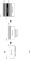
- FIG. 1 shows an example diagram illustrating a process to grow a layered structure with porous multilayer processing for a DBR, according to an illustrative embodiment.
- Process 100 starts at 102 by selecting a substrate 104.
- a portion of substrate is modified as a porous portion 108 a first porosity within the substrate 104.
- the porous portion 108 is generated by exposing an area of substrate 104 to an acid current such that the area of the substrate 104 is etched to form the porous portion 108.
- the first porosity may be configured by controlling the concentration and/or the fluid velocity of the acid current.
- one or more epitaxial layers 112 are epitaxially grown over the porous multilayer 108, where the epitaxial layers 112 can confine an active quantum well cap.
- another porous multilayer 116 having the same porosity with the porous multilayer 108 is created over the supporting layers 112. The second porous multilayer 116 is aligned with the porous multilayer 108 to create a VCSEL.
- This process 100 described in FIG. 1 may be repeated at different spatially separated portions of substrate 104 to form different DBR stacks with different porosities at different regions on the same substrate 104, as shown in FIG. 4 .
- the different porosities allow the substrate to function as a wavelength mirror for multiple wavelengths at the same time.
- the formed different DBR stacks/VCSELs also allow for integration of different devices on a single substrate 104 between the spatially separated DBRs, as further shown in FIGS. 6-7 .
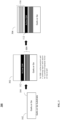
- FIG. 2 shows an example diagram illustrating a process to grow layered structure with an epitaxial DBR layer over a porous multilayer processing for a DBR, according to an illustrative embodiment.
- the process 200 in FIG. 2 can be similar to process 100 in FIG. 1 up to 106 where the substrate has a porous multilayer 108 in a portion of the substrate 104.
- a first epitaxial DBR 204 is grown over the porous multilayer 108
- an active quantum well cap and surrounding layers needed for quantum layer 112 are epitaxially grown over the first epitaxial DBR 204
- a second epitaxial multilayer DBR 202 is grown over the active quantum well and surrounding layers 112.
- the porous reflectivity of porous multilayer DBR 108 may be combined with the epitaxial reflectivity of the first epitaxial DBR 204 to form a chirped epitaxial mirror to engineer reflectivity.
- the porous multilayer 108 and the epitaxial multilayers 204 and 202 of the formed VCSELs operate at the same wavelength and allow a first set of light waves corresponding to a first set of wavelengths to pass through the VCSEL formed at 120 and reflect a second set of light waves of a second set of wavelengths.
- the porous multilayer 108 and epitaxial multilayers 204 and 202 of the formed VCSELs may operate at different wavelengths.
- FIG. 3 shows an example diagram illustrating a process to grow layered structure with porous multilayer processing over an epitaxial layer for a DBR, according to an illustrative embodiment.
- the process 300 in FIG. 3 starts at 102 with the same substrate 104.
- an epitaxial multilayer DBR 304 is grown over substrate 104, the active quantum well cap and surrounding layers needed for quantum layer 112 are epitaxially grown over the epitaxial multilayer DBR 304.
- a porous multilayer 116 is formed over the active quantum well supporting layers 112.
- a second set of epitaxial multilayer DBR may be grown over the active quantum well capping layer 112 to create an epitaxial mirror at the upper portion of the layered structure at 306, which can be similar to the chirped epitaxial mirror formed at step 120 in FIG. 2 but with different compositions of epitaxial DBR or porous DBRs below or above the quantum well cap.
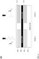
- FIG. 4 shows an example diagram illustrating a layered structure 400 according to an illustrative embodiment.
- the layered structure 400 of FIG. 4 is built on substrate 402.
- Substrate 402 may be similar to substrate 102 described in FIGS. 1-3 .
- the process 100 described in FIG. 1 can be used to form DBR stacks/VSCELs at different regions of the substrate 402, e.g., different spatially separated portions of porous multilayers having different porosities (e.g., see 404, 410) can be formed on the same substrate 402, followed by a single active quantum well capping layer and confining layers needed for quantum layer 406 that are grown over all different portions of the porous GaAs/Ge multilayers 404 and 410.
- porous multilayers 408 and 412 are formed on top of the active quantum well capping layer 406 . Specifically, the additional portions of porous multilayers 408 and 412 are formed to align with porous portions 404 and 410, respectively, and with the same respective porosity. Consequently, as shown in FIG. 4 , multiple VCSELs can be formed on the same substrate 402, e.g., VCSEL 1 and VCSEL 2. It is noted that only two VCSELs are shown in FIG. 4 for illustrative purpose only. Multiple spatially separated VCSELs (more than two) can be formed on the same substrate 402 in a similar way as described above.
- VCSEL 1 illustrates a first layered structure on substrate 402 including a first porous GaAs multilayer 404 having a first porosity over the substrate 402, an active quantum well capping layer 406 epitaxially grown over the first porous GaAs multilayer 104, a second porous GaAs multilayer 408, having the same first porosity, over the active quantum well capping layer 406 aligned with the porous GaAs multilayer 404.
- VCSEL 2 illustrates a third porous GaAs multilayer 410 having a second porosity over the substrate 102, the active quantum well capping layer 406 epitaxially grown over the third porous GaAs multilayer 410, a fourth porous GaAs multilayer 112, having the same second porosity, over the active quantum well capping layer 106 aligned with the second porous GaAs multilayer 410.
- VCSELs configured to operate at different wavelengths can be integrated on a single substrate.
- the integrated VCSELs on the same substrate can yield a wide optical stopband, and provide multiple wavelength mirrors on the same substrate 402.
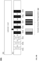
- FIG. 5 shows an embodiment illustrating a layered structure including multiple VCSELs on a single substrate to form a 1-dimensional and/or 2-dimensional array, according to an illustrative embodiment.
- Layered structure 500 shows a substrate and epitaxial VCSEL 502 where an epitaxial DBR and an active quantum well cap and confining layers are epitaxially grown.
- a single bulk wafer 504 to form porous DBRs is grown, where spatially separated porous DBRs of different porosities can be formed, e.g., at portions 506, 508, 510, 512, and 514.
- the porous region 506 has a first porosity
- the porous region 508 has a second porosity
- the porous region 510 has a third porosity
- the porous region 512 has a fourth porosity
- the porous region 514 has a fifth porosity.
- the process of producing different amount of porosity across a single wafer 504 effectively creates a 1-dimensional or 2-dimensional array.
- the epitaxial VCSEL at the substrate 502 may include a DBR with an epitaxial component as described in FIGS. 3-4 .
- the porous DBRs formed by the porous regions 506, 508, 510, 512, or 514 may form a VCSEL by being phase with the epitaxial DBRs in the substrate 502 and portions that are out of phase to suppress the VCSEL.
- FIG. 6 shows an example diagram illustrating an integration of the layered structure 400 described in FIG. 4 with a semiconductor device via a transistor, according to an illustrative embodiment.
- Layered structure 602 includes two VCSELs VCSEL 1 and VCSEL 2 formed on the same substrate 402, which is similar to the layered structure 400 in FIG. 4 .
- FIG. 6 shows a pseudomorphic high-electron-mobility transistor (pHEMT) or a heterojunction bipolar transistor (HBT) integrated in the structure 602.
- pHEMT pseudomorphic high-electron-mobility transistor
- HBT heterojunction bipolar transistor
- the layer above the active quantum well 406 can be a single bulk wafer grown for the purpose of forming the spatially separated porous DBR 408 and 412, and the pHEMT/HBT may be integrated on the single bulk wafer at an available space between the spatially separated DBRs 408 and 412.
- the pHEMT/HBT device can be integrated into the layered structure of VCSELs directly, instead of being added as an external device.
- An example circuit 604 can be formed using the structure 602 with the integrated pHEMT or HBT device. For example, the drain terminal of the HBT is connected with VCSEL 1 and VCSEL 2, via connector 606 as shown in circuit 604.
- FIG. 7a shows an example diagram illustrating a pin diode integrated in a layered structure with two VCSELs formed on the same substrate, according to an illustrative embodiment.
- Layered structure 700 includes two VCSELs VCSEL 1 and VCSEL 2 formed on the same substrate.
- the two VCSELs are formed with porous multilayers having the same porosities, and thus are configured to operate at the same wavelength.
- the porosities of VCSEL 1 and VCSEL 2 help in creating a phased array.
- VCSEL 1 is formed by a first layered structure on substrate 402 including a first porous multilayer 702 having a first porosity over the substrate 402, a first part of an active quantum well capping layer 706 epitaxially grown over the first porous multilayer 702, a first part of an epitaxial DBR 704 grown over the active quantum well capping layer 706.
- VCSEL 2 is formed by a second porous multilayer 708 having a second porosity over the substrate 402, a second part of the same active quantum well capping layer 706 epitaxially grown over the second porous multilayer 708, a second part of the epitaxial DBR 704 grown over the active quantum well capping layer 706.
- the formed VCSELs operate at the same wavelength.
- the porous multilayers or portions 702 and 708 may have different porosities and the formed VCSELs may operate at different wavelengths.
- FIG. 7a shows a pin diode 710 integrated in the structure 700.
- the pin diode 710 is integrated into the substrate 402 at an available space between the spatially separated porous portions 702 and 708.
- the pin diode 710 can be used for power control of the VCSELs.
- FIG. 7b shows an example diagram illustrating a pin diode integrated in a layered structure similar to FIG. 7a but with additional porous structure in the substrate to control light reflectivity of the diode, according to an illustrative embodiment.
- Layered structure 701 is similar to layered structure 700 with porous DBRs 702 and 708 below the active quantum cap 706, and an epitaxial DBR above the active quantum cap 706.
- the epitaxial DBR 704 over the active quantum well capping layer 706 is continuous, light emitted by active quantum well 706 will reflect from this DBR 704 and then impinge on the diode 710 integrated into the substrate 402.
- an additional porous portion 712 may be formed in proximity to the diode 710 to act as a transmission filter for the diode 710, e.g., the porous portion 712 may allow only certain wavelengths to pass through to the diode 710 based on the level of porosity of the porous portion 712.
- the porous portion 712 may be configured with a porosity to pass through the same wavelength ⁇ 1 , and thus a device of zero reflectivity at the wavelength ⁇ 1 can be achieved.
- a portion of the epitaxial DBR 704 may be modified using the porous process described above to form a porous portion 713, which can be substantially aligned with the location where the pin diode 710 is integrated such that the porous portion 713 is placed at a position to reflect light waves emitted from the quantum well cap 706 to the pin diode 710.
- porosity of the porous portion 713 may be controlled to yield a reflectivity property to match the reflectivity property of pin diode 710.
- the porous portion 713 may be more responsive to light waves at wavelength ⁇ 1 emitted from the active quantum well 706, and the reflected light waves can then pass through the porous structure 712 to reach the pin diode 710.
- additional devices such as a HBT or a diode can be integrated into the substrate of the VCSELs directly, instead of adding the additional devices as an external device to the VCSEL. In this way, circuit area may be more efficiently consumed.
- FIG. 8A shows an example diagram illustrates a process to create cross-section DBRs via porous multilayer processing, according to an illustrative embodiment.
- the process 800a in FIG. 8A begins with the layered structure 114 created via a similar process 100 as illustrated in FIG. 1 .
- the layered structure 114 is a VCSEL comprising a first porous portion 108 over a substrate 104 and a second porous portion 116 over an epitaxial active quantum well layer 112 grown over the first porous portion 108.
- a first vertical portion (e.g., vertical epitaxial DBR) 804 and a second vertical portion (e.g., vertical epitaxial DBR) 806 of the VCSEL 114 are formed to cross the porous DBRs 108 and 116.
- the original continuous porous DBRs 108 and 116 are interrupted, and sectioned by the vertical DBRs 804 and 806 to form different porous portions of different porosities, respectively.
- the vertical porous processing e.g., the first vertical portion 804 and the second vertical portion 806, is not dependent on the presence of the first porous portion 108 over a substrate 104 and a second porous portion 116 over an epitaxial active quantum well layer 112 grown over the first porous portion 108.
- FIG. 8B shows an example diagram illustrates a process to create cross-section DBRs via porous multilayer processing, according to an illustrative embodiment.
- Process 800b starts at 808 with a substrate and VCSEL 810, e.g., the VCSEL may be similar to those described throughout FIGS. 1-7B .
- the substrate 808 may not contain a VCSEL.
- various portions of the substrate 810 are modified to form vertical porous portions, e.g., see 810a-h, which separate areas on the substrate 808, so as to produce clearly defined VCSELs V1-V7, respectively.
- the porosity of the porous portions 810a-h can be chosen to achieve different functions.
- the porosity of a porous portions can be chosen to block one or more wavelengths so as to isolate VCSELs on different sides of the respective porous region, e.g., see 810d-810h.
- the porosities of the vertical porous portions of the substrate 808 may be chosen to form porous filters, e.g., 810a-c.
- the porous filters may be composed of different thicknesses and different porosities to create different porous filters that may pass through certain wavelengths of light based on composition 808and combination of the porous filters.
- a combination of porous filters (e.g. 810a-c) and porous isolation regions (e.g. 810d-h) may be used together between adjacent VCSELS to allow some level of optical mixing.
- FIG. 9 shows an example diagram illustrating a focused VCSEL including a radial porous DBR, according to an illustrative embodiment.
- Circular structure 900 depicts a circular substrate 902.
- the circular structure 900 includes a radial porous DBR 904, a radial quantum well cap, and additional radial DBRs (e.g., porous or epitaxial, or a combination of both as described in FIGS. 2-3 but in a radial form) within the circular substrate 902 to form a focused VCSEL.
- additional radial DBRs e.g., porous or epitaxial, or a combination of both as described in FIGS. 2-3 but in a radial form
- porous DBRs shown in FIGs. 1-9 may include a porous layer of the same thickness and porosity. In some embodiments, it is possible that both the thickness and the porosity of the porous layer may be varied through a DBR region thereby creating more complex reflectivity spectra.
- the growth and/or deposition described herein may be performed using one or more of chemical vapor deposition (CVD), metalorganic chemical vapor deposition (MOCVD), organometallic vapor phase epitaxy (OMVPE), atomic layer deposition (ALD), molecular beam epitaxy (MBE), halide vapor phase epitaxy (HVPE), pulsed laser deposition (PLD), and/or physical vapor deposition (PVD).
- CVD chemical vapor deposition
- MOCVD metalorganic chemical vapor deposition
- OMVPE organometallic vapor phase epitaxy
- ALD atomic layer deposition
- MBE molecular beam epitaxy
- HVPE halide vapor phase epitaxy
- PLD pulsed laser deposition
- PVD physical vapor deposition
- a layer means a substantially-uniform thickness of a material covering a surface.
- a layer can be either continuous or discontinuous (i.e., having gaps between regions of the material).
- a layer can completely or partially cover a surface, or be segmented into discrete regions, which collectively define the layer (i.e., regions formed using selective-area epitaxy).
- Monolithically-integrated means formed on the surface of the substrate, typically by depositing layers disposed on the surface.
- This layer may comprise intermediate layers, such as transitional layers, necessary to ensure a suitable surface.
- This layer can mean either (1) the material is in intimate contact with the substrate; or (2) the material is in contact with one or more transitional layers that reside on the substrate.
- Single-crystal means a crystalline structure that comprises substantially only one type of unit-cell.
- a single-crystal layer may exhibit some crystalline defects such as stacking faults, dislocations, or other commonly occurring crystalline defects.
- Single-domain means a crystalline structure that comprises substantially only one structure of unit-cell and substantially only one orientation of that unit cell. In other words, a single-domain crystal exhibits no twinning or anti-phase domains.
- Single-phase means a crystalline structure that is both single-crystal and single-domain.
- Substrate means the material on which deposited layers are formed.
- Exemplary substrates include, without limitation: bulk silicon wafers, in which a wafer comprises a homogeneous thickness of single-crystal silicon; composite wafers, such as a silicon-on-insulator wafer that comprises a layer of silicon that is disposed on a layer of silicon dioxide that is disposed on a bulk silicon handle wafer; or any other material that serves as base layer upon which, or in which, devices are formed.
- a substrate may have a single bulk wafer, or multiple sub-layers.
- a substrate may include multiple non-continuous porous portions. The multiple non-continuous porous portions may have different densities and may be horizontally distributed or vertically layered. The invention is restricted to a Ge substrate.
- Miscut Substrate means a substrate which comprises a surface crystal structure that is oriented at an angle to that associated with the crystal structure of the substrate.
- a 6° miscut ⁇ 100> silicon wafer comprises a ⁇ 100> silicon wafer that has been cut at an angle to the ⁇ 100> crystal orientation by 6° toward another major crystalline orientation, such as ⁇ 110>.
- the miscut will be up to about 20°.
- the phrase "miscut substrate” includes miscut wafers having any major crystal orientation. That is, a ⁇ 111> wafer miscut toward the ⁇ 011> direction, a ⁇ 100> wafer miscut toward the ⁇ 110> direction, and a ⁇ 011> wafer miscut toward the ⁇ 001> direction.
- Semiconductor refers to any solid substance that has a conductivity between that of an insulator and that of most metals.
- An example semiconductor layer is composed of silicon.
- the semiconductor layer may include a single bulk wafer, or multiple sub-layers.
- a silicon semiconductor layer may include multiple non-continuous porous portions. The multiple non-continuous porous portions may have different densities and may be horizontally distributed or vertically layered.
- Semiconductor-on-Insulator means a composition that comprises a single-crystal semiconductor layer, a single-phase dielectric layer, and a substrate, wherein the dielectric layer is interposed between the semiconductor layer and the substrate.
- SOI silicon-on-insulator
- This structure is pronounced of prior-art silicon-on-insulator ("SOI") compositions, which typically include a single-crystal silicon substrate, a non-single-phase dielectric layer (e.g., amorphous silicon dioxide, etc.) and a single-crystal silicon semiconductor layer.
- SOI silicon-on-insulator
- Semiconductor-on-insulator compositions include a dielectric layer that has a single-phase morphology, whereas SOI wafers do not. In fact, the insulator layer of typical SOI wafers is not even single crystal.
- Semiconductor-on-insulator compositions include a silicon, germanium, or silicon-germanium "active" layer, whereas prior-art SOI wafers use a silicon active layer.
- exemplary semiconductor-on-insulator compositions include, without limitation: silicon-on-insulator, germanium-on-insulator, and silicon-germanium-on-insulator.
- a first layer described and/or depicted herein as “configured on,” “on” or “over” a second layer can be immediately adjacent to the second layer, or one or more intervening layers can be between the first and second layers.
- a first layer that is described and/or depicted herein as “directly on” or “directly over” a second layer or a substrate is immediately adjacent to the second layer or substrate with no intervening layer present, other than possibly an intervening alloy layer that may form due to mixing of the first layer with the second layer or substrate.
- a first layer that is described and/or depicted herein as being “on,” “over,” “directly on,” or “directly over” a second layer or substrate may cover the entire second layer or substrate, or a portion of the second layer or substrate.
- a substrate is placed on a substrate holder during layer growth, and so a top surface or an upper surface is the surface of the substrate or layer furthest from the substrate holder, while a bottom surface or a lower surface is the surface of the substrate or layer nearest to the substrate holder.
- Any of the structures depicted and described herein can be part of larger structures with additional layers above and/or below those depicted. For clarity, the figures herein can omit these additional layers, although these additional layers can be part of the structures disclosed. In addition, the structures depicted can be repeated in units, even if this repetition is not depicted in the figures.
Landscapes
- Physics & Mathematics (AREA)
- Condensed Matter Physics & Semiconductors (AREA)
- General Physics & Mathematics (AREA)
- Electromagnetism (AREA)
- Optics & Photonics (AREA)
- Semiconductor Lasers (AREA)
Claims (17)
- Geschichtete Struktur, die Folgendes umfasst:ein Substrat (104), das aus Germanium besteht, einschließlich einer ersten porösen Mehrfachschicht (108) mit einer ersten Porosität;eine aktive Quantentopfdeckschicht (112), die epitaktisch über der ersten porösen Mehrfachschicht aufgewachsen ist;eine zweite poröse Mehrfachschicht (116) mit der ersten Porosität über der aktiven Quantentopfdeckschicht,wobei Ränder der zweiten porösen Mehrfachschicht (116) mit Rändern der ersten porösen Mehrfachschicht (108) ausgerichtet sind.
- Geschichtete Struktur nach Anspruch 1, wobei ein Stapel aus der ersten porösen Mehrfachschicht, wenigstens einem ersten Teil der aktiven Quantentopfdeckschicht, der mit der ersten porösen Mehrfachschicht ausgerichtet ist, und der zweiten porösen Mehrfachschicht ermöglicht, dass eine erste Lichtwelle mit einer ersten Wellenlänge durch den Stapel hindurchgeht.
- Geschichtete Struktur nach Anspruch 1, die ferner Folgendes umfasst:eine erste epitaktische Bragg-Spiegel-Mehrfachschicht, die über dem Substrat zwischen der ersten porösen Mehrfachschicht und der aktiven Quantentopfdeckschicht aufgewachsen ist,wobei die zweite poröse Mehrfachschicht eine zweite epitaktische Bragg-Spiegel-Mehrfachschicht über der aktiven Quantentopfdeckschicht beinhaltet, undwobei ein erster Reflexionsgrad der ersten epitaktischen Bragg-Spiegel-Mehrfachschicht verschieden von einem zweiten Reflexionsgrad der zweiten epitaktischen Bragg-Spiegel-Mehrfachschicht ist, wodurch bewirkt wird, dass ein Stapel aus der ersten porösen Mehrfachschicht, der ersten epitaktischen Bragg-Spiegel-Mehrfachschicht und der zweiten epitaktischen Bragg-Spiegel-Mehrfachschicht ermöglicht, dass eine erste Lichtwelle mit einer ersten Wellenlänge durch den Stapel hindurchgeht.
- Geschichtete Struktur nach Anspruch 1, wobei die erste poröse Mehrfachschicht (404) und die zweite poröse Mehrfachschicht (408) mit einem ersten Gebiet auf der aktiven Quantentopfdeckschicht (406) ausgerichtet sind und das Substrat eine dritte poröse Mehrfachschicht (410) mit einer zweiten Porosität beinhaltet, und
wobei die geschichtete Struktur ferner Folgendes umfasst:eine vierte poröse Mehrfachschicht (412) mit der zweiten Porosität über der aktiven Quantentopfdeckschicht (406), wobei die zweite poröse Mehrfachschicht (408) und die vierte poröse Mehrfachschicht (412) poröse Teile einer Volumenschicht sind, die über der aktiven Quantentopfdeckschicht (406) aufgewachsen ist, undwobei die dritte poröse Mehrfachschicht (410) und die vierte poröse Mehrfachschicht (4120 mit einem zweiten Gebiet auf der aktiven Quantentopfdeckschicht (406) ausgerichtet sind. - Geschichtete Struktur nach Anspruch 4, wobei die erste poröse Mehrfachschicht und die dritte poröse Mehrfachschicht unterschiedliche Abmessungen oder unterschiedliche Porositäten aufweisen, und
die zweite poröse Mehrfachschicht und die vierte poröse Mehrfachschicht unterschiedliche Abmessungen oder unterschiedliche Porositäten aufweisen. - Geschichtete Struktur nach Anspruch 4, wobei die erste poröse Mehrfachschicht, wenigstens das erste Gebiet der aktiven Quantentopfdeckschicht und die zweite poröse Mehrfachschicht einen ersten VCSEL bilden, der ermöglicht, dass eine erste Lichtwelle mit einer ersten Wellenlänge hindurchgeht, und die dritte poröse Mehrfachschicht, wenigstens das zweite Gebiet der aktiven Quantentopfdeckschicht und die vierte poröse Mehrfachschicht einen zweiten VCSEL bilden, der ermöglicht, dass eine zweite Lichtwelle mit einer zweiten Wellenlänge hindurchgeht.
- Geschichtete Struktur nach Anspruch 1, wobei die zweite poröse Mehrfachschicht ein poröser Teil einer Volumenschicht ist, die über der aktiven Quantentopfdeckschicht aufgewachsen ist, und
wobei die Volumenschicht mehrere räumlich verteilte poröse Mehrfachschichten aufweist, wobei jede poröse Mehrfachschicht von den mehreren eine Porosität aufweist, die zum Erhalten eines speziellen Reflexionsgrades der jeweiligen porösen Mehrfachschicht ausgewählt ist, um zu ermöglichen, dass eine Lichtwelle mit einer speziellen Wellenlänge hindurchgeht. - Geschichtete Struktur nach Anspruch 4, die ferner Folgendes umfasst:
einen pseudomorphischen Transistor mit hoher Elektronenbeweglichkeit oder einen Heteroübergang-Bipolartransistor, der in die Volumenschicht in einem Raum zwischen der zweiten porösen Mehrfachschicht und der vierten porösen Mehrfachschicht integriert ist. - Geschichtete Struktur nach Anspruch 6,
wobei die zweite poröse Mehrfachschicht und die vierte poröse Mehrfachschicht eine gleiche Porosität aufweisen und miteinander als eine kontinuierliche poröse Mehrfachschicht in der Volumenschicht verbunden sind. - Geschichtete Struktur nach Anspruch 9, die ferner Folgendes umfasst:
eine pin-Diode, die in das Substrat in einem Raum zwischen der ersten porösen Mehrfachschicht und der dritten porösen Mehrfachschicht integriert ist. - Geschichtete Struktur nach Anspruch 10, wobei die kontinuierliche poröse Mehrfachschicht eine fünfte poröse Mehrfachschicht beinhaltet, die mit der pin-Diode ausgerichtet ist, und die fünfte poröse Mehrfachschicht eine dritte Porosität aufweist, die ermöglicht, dass die fünfte poröse Mehrfachschicht die erste Lichtwelle mit der ersten Wellenlänge, die von der aktiven Quantentopfdeckschicht emittiert wird, in eine Richtung der pin-Diode reflektiert.
- Geschichtete Struktur nach Anspruch 11, wobei das Substrat eine sechste poröse Mehrfachschicht in der Nähe der pin-Diode beinhaltet und die sechste poröse Mehrfachschicht zum Ermöglichen davon konfiguriert ist, dass die erste Lichtwelle mit der ersten Wellenlänge hindurchgeht, um die pin-Diode zu erreichen.
- Geschichtete Struktur nach Anspruch 1, die ferner Folgendes umfasst:einen oder mehrere vertikale poröse Mehrschichtteile (804, 806, 810a-h) senkrecht zu und hinweg über die erste poröse Mehrfachschicht, die aktive Quantentopfdeckschicht und die zweite poröse Mehrfachschicht,wobei die eine oder die mehreren vertikalen porösen Mehrfachschichtteile einen Stapel aus der ersten porösen Mehrfachschicht, der aktiven Quantentopfdeckschicht und der zweiten porösen Mehrfachschicht unterteilen, um mehrere VCSELs zu bilden.
- Geschichtete Struktur nach Anspruch 13, wobei Dicke und Porosität wenigstens eines vertikalen porösen Mehrfachschichtteils ausgewählt werden, um ein poröses Filter zu bilden, das ermöglicht, dass eine dritte Lichtwelle mit einer dritten Wellenlänge zwischen zwei angrenzenden VCSELs von den mehreren VCSELs hindurchgeht.
- Geschichtete Struktur nach Anspruch 13, wobei Dicke und Porosität wenigstens eines vertikalen porösen Mehrfachschichtteils ausgewählt werden, um eine poröse Isolation zu bilden, die keiner Lichtwelle einen Durchgang zwischen zwei angrenzenden VCSELs von den mehreren VCSELs erlaubt.
- Geschichtete Struktur, die Folgendes umfasst:ein Substrat (104), das aus Germanium besteht;eine erste epitaktische Bragg-Spiegel-Mehrfachschicht (204), die über dem Substrat (104) aufgewachsen ist;eine aktive Quantentopfdeckschicht (112), die epitaktisch über der ersten epitaktischen Bragg-Spiegel-Mehrfachschicht (204) aufgewachsen ist; undeine poröse Mehrfachschicht, die aus einem gleichen Material wie das Substrat besteht, wobei sich die poröse Mehrfachschicht über der aktiven Quantentopfschicht befindet.
- Geschichtete Struktur nach Anspruch 16, die ferner Folgendes umfasst:eine zweite epitaktische Bragg-Spiegel-Mehrfachschicht (202), die über dem aktiven Quantentopf (112) und zwischen dem aktiven Quantentopf und der porösen Mehrfachschicht aufgewachsen ist,wobei ein erster Reflexionsgrad der ersten epitaktischen Bragg-Spiegel-Mehrfachschicht verschieden von einem zweiten Reflexionsgrad der zweiten epitaktischen Bragg-Spiegel-Mehrfachschicht ist, wodurch bewirkt wird, dass ein Stapel aus der porösen Mehrfachschicht, der ersten epitaktischen Bragg-Spiegel-Mehrfachschicht und der zweiten epitaktischen Bragg-Spiegel-Mehrfachschicht ermöglicht, dass eine erste Lichtwelle mit einer ersten Wellenlänge durch den Stapel hindurchgeht.
Priority Applications (1)
| Application Number | Priority Date | Filing Date | Title |
|---|---|---|---|
| EP23152877.9A EP4213319B1 (de) | 2018-01-18 | 2019-01-18 | Poröse verteilte bragg-reflektoren für laseranwendungen |
Applications Claiming Priority (2)
| Application Number | Priority Date | Filing Date | Title |
|---|---|---|---|
| US201862618985P | 2018-01-18 | 2018-01-18 | |
| PCT/US2019/014204 WO2019143945A1 (en) | 2018-01-18 | 2019-01-18 | Porous distributed bragg reflectors for laser applications |
Related Child Applications (2)
| Application Number | Title | Priority Date | Filing Date |
|---|---|---|---|
| EP23152877.9A Division EP4213319B1 (de) | 2018-01-18 | 2019-01-18 | Poröse verteilte bragg-reflektoren für laseranwendungen |
| EP23152877.9A Division-Into EP4213319B1 (de) | 2018-01-18 | 2019-01-18 | Poröse verteilte bragg-reflektoren für laseranwendungen |
Publications (2)
| Publication Number | Publication Date |
|---|---|
| EP3741015A1 EP3741015A1 (de) | 2020-11-25 |
| EP3741015B1 true EP3741015B1 (de) | 2023-06-07 |
Family
ID=65352146
Family Applications (2)
| Application Number | Title | Priority Date | Filing Date |
|---|---|---|---|
| EP19704126.2A Active EP3741015B1 (de) | 2018-01-18 | 2019-01-18 | Poröse verteilte bragg-reflektoren für laseranwendungen |
| EP23152877.9A Active EP4213319B1 (de) | 2018-01-18 | 2019-01-18 | Poröse verteilte bragg-reflektoren für laseranwendungen |
Family Applications After (1)
| Application Number | Title | Priority Date | Filing Date |
|---|---|---|---|
| EP23152877.9A Active EP4213319B1 (de) | 2018-01-18 | 2019-01-18 | Poröse verteilte bragg-reflektoren für laseranwendungen |
Country Status (8)
| Country | Link |
|---|---|
| US (1) | US11201451B2 (de) |
| EP (2) | EP3741015B1 (de) |
| JP (1) | JP2021511662A (de) |
| KR (1) | KR20200111724A (de) |
| CN (1) | CN111630735B (de) |
| SG (1) | SG11202005786SA (de) |
| TW (1) | TWI827578B (de) |
| WO (1) | WO2019143945A1 (de) |
Families Citing this family (8)
| Publication number | Priority date | Publication date | Assignee | Title |
|---|---|---|---|---|
| CN106848838B (zh) * | 2017-04-06 | 2019-11-29 | 中国科学院半导体研究所 | 基于多孔DBR的GaN基VCSEL芯片及制备方法 |
| US10868213B2 (en) * | 2018-06-26 | 2020-12-15 | Lumileds Llc | LED utilizing internal color conversion with light extraction enhancements |
| US12007504B2 (en) | 2019-03-01 | 2024-06-11 | Vixar, Inc. | 3D and LiDAR sensing modules |
| KR102866073B1 (ko) * | 2020-11-27 | 2025-09-30 | 삼성전자주식회사 | 공간 광변조기 및 그 제조방법, 공간 광변조기를 포함하는 라이다 장치 |
| GB2612040B (en) * | 2021-10-19 | 2025-02-12 | Iqe Plc | Porous distributed Bragg reflector apparatuses, systems, and methods |
| WO2024044998A1 (en) * | 2022-08-30 | 2024-03-07 | Huawei Technologies Co., Ltd. | Low-coherence surface-emitting laser (lcsel) |
| US20240222552A1 (en) * | 2023-01-04 | 2024-07-04 | Innolux Corporation | Semiconductor element, electronic device comprising semiconductor element, and semiconductor chip |
| CN116093738B (zh) * | 2023-02-27 | 2026-02-06 | 中国科学院半导体研究所 | 垂直腔面发射激光器及其制备方法 |
Citations (1)
| Publication number | Priority date | Publication date | Assignee | Title |
|---|---|---|---|---|
| US20170237234A1 (en) * | 2014-09-30 | 2017-08-17 | Yale University | A method for gan vertical microcavity surface emitting laser (vcsel) |
Family Cites Families (37)
| Publication number | Priority date | Publication date | Assignee | Title |
|---|---|---|---|---|
| US5283447A (en) * | 1992-01-21 | 1994-02-01 | Bandgap Technology Corporation | Integration of transistors with vertical cavity surface emitting lasers |
| US5306385A (en) * | 1992-09-15 | 1994-04-26 | Texas Instruments Incorporated | Method for generating photoluminescence emission lines from transition element doped CAF2 thin films over a Si-based substrate |
| GB2347558B (en) | 1995-11-30 | 2000-11-15 | Hewlett Packard Co | Vertical cavity surface emitting lasers |
| US5939732A (en) * | 1997-05-22 | 1999-08-17 | Kulite Semiconductor Products, Inc. | Vertical cavity-emitting porous silicon carbide light-emitting diode device and preparation thereof |
| DE19807783A1 (de) * | 1998-02-18 | 1999-09-02 | Siemens Ag | Bauelement mit einem Lichtsender und einem Lichtempfänger |
| US6376269B1 (en) * | 1999-02-02 | 2002-04-23 | Agilent Technologies, Inc. | Vertical cavity surface emitting laser (VCSEL) using buried Bragg reflectors and method for producing same |
| US6746777B1 (en) * | 2000-05-31 | 2004-06-08 | Applied Optoelectronics, Inc. | Alternative substrates for epitaxial growth |
| KR100754156B1 (ko) * | 2000-08-23 | 2007-09-03 | 삼성전자주식회사 | 다중 파장 표면광 레이저 및 그 제조방법 |
| US6549556B1 (en) * | 2000-12-01 | 2003-04-15 | Applied Optoelectronics, Inc. | Vertical-cavity surface-emitting laser with bottom dielectric distributed bragg reflector |
| JP2002246695A (ja) * | 2001-02-13 | 2002-08-30 | Canon Inc | 多孔質基板を用いた半導体デバイスの作製法及び半導体デバイス |
| US20020163688A1 (en) * | 2001-03-26 | 2002-11-07 | Zuhua Zhu | Optical communications system and vertical cavity surface emitting laser therefor |
| US20020179930A1 (en) * | 2001-06-01 | 2002-12-05 | Motorola, Inc. | Composite semiconductor structure and device with optical testing elements |
| US6697413B2 (en) * | 2001-10-31 | 2004-02-24 | Applied Optoelectronics, Inc. | Tunable vertical-cavity surface-emitting laser with tuning junction |
| US6850548B2 (en) * | 2001-12-28 | 2005-02-01 | Finisar Corporation | Assymmetric distributed Bragg reflector for vertical cavity surface emitting lasers |
| US6771680B2 (en) * | 2002-10-22 | 2004-08-03 | Agilent Technologies, Inc | Electrically-pumped, multiple active region vertical-cavity surface-emitting laser (VCSEL) |
| GB2399940A (en) * | 2003-03-25 | 2004-09-29 | Sharp Kk | Vertical cavity surface emitting laser |
| JP4235530B2 (ja) * | 2003-10-20 | 2009-03-11 | キヤノン株式会社 | 面発光型ダイオード、面発光型ダイオードアレイ及びその製造方法 |
| JP4138629B2 (ja) * | 2003-11-06 | 2008-08-27 | 株式会社東芝 | 面発光型半導体素子及びその製造方法 |
| JP4833665B2 (ja) * | 2004-02-17 | 2011-12-07 | 古河電気工業株式会社 | フォトニック結晶半導体デバイスの製造方法 |
| JP4710282B2 (ja) * | 2004-09-06 | 2011-06-29 | 富士ゼロックス株式会社 | 多波長面発光レーザの製造方法 |
| JP4568125B2 (ja) * | 2005-01-17 | 2010-10-27 | 株式会社東芝 | 面発光型半導体素子 |
| JP4027392B2 (ja) * | 2005-04-28 | 2007-12-26 | キヤノン株式会社 | 垂直共振器型面発光レーザ装置 |
| JP4919628B2 (ja) * | 2005-07-28 | 2012-04-18 | 株式会社リコー | 面発光レーザ及び面発光レーザアレイ及び光書き込みシステム及び光伝送システム |
| US7499481B2 (en) * | 2006-11-14 | 2009-03-03 | Canon Kabushiki Kaisha | Surface-emitting laser and method for producing the same |
| JP4235674B2 (ja) * | 2006-11-14 | 2009-03-11 | キヤノン株式会社 | 面発光レーザ装置およびその製造方法 |
| JP2009170508A (ja) | 2008-01-11 | 2009-07-30 | Furukawa Electric Co Ltd:The | 面発光半導体レーザ及びその製造方法 |
| CN102782818B (zh) | 2010-01-27 | 2016-04-27 | 耶鲁大学 | 用于GaN装置的基于导电性的选择性蚀刻和其应用 |
| WO2013016676A2 (en) * | 2011-07-27 | 2013-01-31 | MYTEK, LLC (doing business as VIXAR) | Method and apparatus including improved vertical-cavity surface-emitting lasers |
| KR101272833B1 (ko) * | 2012-02-03 | 2013-06-11 | 광주과학기술원 | 실리콘 dbr 구조가 집적된 광 소자 및 그 제조방법 |
| US9583353B2 (en) * | 2012-06-28 | 2017-02-28 | Yale University | Lateral electrochemical etching of III-nitride materials for microfabrication |
| US20170093128A1 (en) * | 2014-03-04 | 2017-03-30 | Hewlett Packard Enterprise Development Lp | Vertical-cavity surface-emitting lasers |
| US11095096B2 (en) * | 2014-04-16 | 2021-08-17 | Yale University | Method for a GaN vertical microcavity surface emitting laser (VCSEL) |
| RU2645805C1 (ru) * | 2014-09-25 | 2018-02-28 | Конинклейке Филипс Н.В. | Лазер с вертикальным резонатором и поверхностным излучением |
| US10790410B2 (en) * | 2015-10-23 | 2020-09-29 | Sensor Electronic Technology, Inc. | Light extraction from optoelectronic device |
| US11495670B2 (en) * | 2016-09-22 | 2022-11-08 | Iqe Plc | Integrated epitaxial metal electrodes |
| CN106848838B (zh) * | 2017-04-06 | 2019-11-29 | 中国科学院半导体研究所 | 基于多孔DBR的GaN基VCSEL芯片及制备方法 |
| US11038321B2 (en) * | 2018-10-12 | 2021-06-15 | The Board Of Trustees Of The University Of Illinois | Single mode VCSELs with low threshold and high speed operation |
-
2019
- 2019-01-18 CN CN201980008703.XA patent/CN111630735B/zh active Active
- 2019-01-18 KR KR1020207023497A patent/KR20200111724A/ko not_active Abandoned
- 2019-01-18 SG SG11202005786SA patent/SG11202005786SA/en unknown
- 2019-01-18 US US16/252,334 patent/US11201451B2/en active Active
- 2019-01-18 TW TW108102069A patent/TWI827578B/zh active
- 2019-01-18 JP JP2020539230A patent/JP2021511662A/ja active Pending
- 2019-01-18 EP EP19704126.2A patent/EP3741015B1/de active Active
- 2019-01-18 EP EP23152877.9A patent/EP4213319B1/de active Active
- 2019-01-18 WO PCT/US2019/014204 patent/WO2019143945A1/en not_active Ceased
Patent Citations (1)
| Publication number | Priority date | Publication date | Assignee | Title |
|---|---|---|---|---|
| US20170237234A1 (en) * | 2014-09-30 | 2017-08-17 | Yale University | A method for gan vertical microcavity surface emitting laser (vcsel) |
Non-Patent Citations (1)
| Title |
|---|
| "Selective oxidation of buried AlGaAs versus AlAs layers", APPLIED PHYSICS LETTERS, AMERICAN INSTITUTE OF PHYSICS, 2 HUNTINGTON QUADRANGLE, MELVILLE, NY 11747, vol. 69, no. 10, 2 September 1996 (1996-09-02), pages 1385 - 1387, XP012016006, ISSN: 0003-6951, DOI: 10.1063/1.117589 * |
Also Published As
| Publication number | Publication date |
|---|---|
| WO2019143945A1 (en) | 2019-07-25 |
| TWI827578B (zh) | 2024-01-01 |
| EP4213319A1 (de) | 2023-07-19 |
| US11201451B2 (en) | 2021-12-14 |
| EP3741015A1 (de) | 2020-11-25 |
| EP4213319B1 (de) | 2024-08-14 |
| KR20200111724A (ko) | 2020-09-29 |
| TW201941271A (zh) | 2019-10-16 |
| CN111630735B (zh) | 2024-07-26 |
| SG11202005786SA (en) | 2020-08-28 |
| JP2021511662A (ja) | 2021-05-06 |
| US20190221993A1 (en) | 2019-07-18 |
| CN111630735A (zh) | 2020-09-04 |
Similar Documents
| Publication | Publication Date | Title |
|---|---|---|
| US11201451B2 (en) | Porous distributed Bragg reflectors for laser applications | |
| US8502263B2 (en) | Light-emitter-based devices with lattice-mismatched semiconductor structures | |
| US6320206B1 (en) | Light emitting devices having wafer bonded aluminum gallium indium nitride structures and mirror stacks | |
| US6280523B1 (en) | Thickness tailoring of wafer bonded AlxGayInzN structures by laser melting | |
| EP1326290B1 (de) | Verfahren zur Herstellung von Halbleitervorrichtungen | |
| US6177359B1 (en) | Method for detaching an epitaxial layer from one substrate and transferring it to another substrate | |
| US6878958B2 (en) | Vertical cavity surface emitting laser with buried dielectric distributed Bragg reflector | |
| EP1182756A2 (de) | Halbleiterlaservorrichtung mit niedrigem Schwellstrom | |
| CN115298914B (zh) | 形成垂直腔面发射激光器的光学孔径的方法和垂直腔面发射激光器 | |
| WO2000038287A1 (en) | Mechanical stabilization of lattice mismatched quantum wells | |
| US20070160100A1 (en) | Misfit dislocation forming interfacial self-assembly for growth of highly-mismatched III-Sb alloys | |
| US11005231B2 (en) | Strain-balanced semiconductor structure | |
| KR20100080829A (ko) | 양자 웰 혼합 | |
| US6858519B2 (en) | Atomic hydrogen as a surfactant in production of highly strained InGaAs, InGaAsN, InGaAsNSb, and/or GaAsNSb quantum wells | |
| US20210257809A1 (en) | Strain-balanced semiconductor structure | |
| US20070164311A1 (en) | Ingaas/gaas lasers on-silicon produced by-lepecvd and mocvd | |
| JPH11121864A (ja) | 面発光レーザ及びその製造方法 | |
| EP3896850A1 (de) | Schichtstruktur mit bereichen lokalisierter spannung in kristallinen seltenerdoxiden | |
| EP0944143A1 (de) | Oberflächenemittierender laser und dessen herstellungsverfahren | |
| JP2005252111A (ja) | 半導体装置 | |
| JP2022517537A (ja) | 集積化エピタキシャル金属電極 | |
| US11025029B2 (en) | Monolithic III-V nanolaser on silicon with blanket growth | |
| KR20100067961A (ko) | 다채널 표면 방출 레이저 및 그의 제조 방법 | |
| Speier | MOVPE for optoelectronics | |
| JPH11220207A (ja) | 多波長面発光半導体レーザ装置の製造方法 |
Legal Events
| Date | Code | Title | Description |
|---|---|---|---|
| STAA | Information on the status of an ep patent application or granted ep patent |
Free format text: STATUS: UNKNOWN |
|
| STAA | Information on the status of an ep patent application or granted ep patent |
Free format text: STATUS: THE INTERNATIONAL PUBLICATION HAS BEEN MADE |
|
| PUAI | Public reference made under article 153(3) epc to a published international application that has entered the european phase |
Free format text: ORIGINAL CODE: 0009012 |
|
| STAA | Information on the status of an ep patent application or granted ep patent |
Free format text: STATUS: REQUEST FOR EXAMINATION WAS MADE |
|
| 17P | Request for examination filed |
Effective date: 20200721 |
|
| AK | Designated contracting states |
Kind code of ref document: A1 Designated state(s): AL AT BE BG CH CY CZ DE DK EE ES FI FR GB GR HR HU IE IS IT LI LT LU LV MC MK MT NL NO PL PT RO RS SE SI SK SM TR |
|
| AX | Request for extension of the european patent |
Extension state: BA ME |
|
| DAV | Request for validation of the european patent (deleted) | ||
| DAX | Request for extension of the european patent (deleted) | ||
| STAA | Information on the status of an ep patent application or granted ep patent |
Free format text: STATUS: EXAMINATION IS IN PROGRESS |
|
| 17Q | First examination report despatched |
Effective date: 20220211 |
|
| GRAP | Despatch of communication of intention to grant a patent |
Free format text: ORIGINAL CODE: EPIDOSNIGR1 |
|
| STAA | Information on the status of an ep patent application or granted ep patent |
Free format text: STATUS: GRANT OF PATENT IS INTENDED |
|
| INTG | Intention to grant announced |
Effective date: 20220923 |
|
| GRAS | Grant fee paid |
Free format text: ORIGINAL CODE: EPIDOSNIGR3 |
|
| GRAA | (expected) grant |
Free format text: ORIGINAL CODE: 0009210 |
|
| STAA | Information on the status of an ep patent application or granted ep patent |
Free format text: STATUS: THE PATENT HAS BEEN GRANTED |
|
| AK | Designated contracting states |
Kind code of ref document: B1 Designated state(s): AL AT BE BG CH CY CZ DE DK EE ES FI FR GB GR HR HU IE IS IT LI LT LU LV MC MK MT NL NO PL PT RO RS SE SI SK SM TR |
|
| REG | Reference to a national code |
Ref country code: GB Ref legal event code: FG4D |
|
| P01 | Opt-out of the competence of the unified patent court (upc) registered |
Effective date: 20230321 |
|
| REG | Reference to a national code |
Ref country code: CH Ref legal event code: EP Ref country code: AT Ref legal event code: REF Ref document number: 1577750 Country of ref document: AT Kind code of ref document: T Effective date: 20230615 |
|
| REG | Reference to a national code |
Ref country code: DE Ref legal event code: R096 Ref document number: 602019030038 Country of ref document: DE |
|
| REG | Reference to a national code |
Ref country code: LT Ref legal event code: MG9D |
|
| REG | Reference to a national code |
Ref country code: NL Ref legal event code: MP Effective date: 20230607 |
|
| PG25 | Lapsed in a contracting state [announced via postgrant information from national office to epo] |
Ref country code: SE Free format text: LAPSE BECAUSE OF FAILURE TO SUBMIT A TRANSLATION OF THE DESCRIPTION OR TO PAY THE FEE WITHIN THE PRESCRIBED TIME-LIMIT Effective date: 20230607 Ref country code: NO Free format text: LAPSE BECAUSE OF FAILURE TO SUBMIT A TRANSLATION OF THE DESCRIPTION OR TO PAY THE FEE WITHIN THE PRESCRIBED TIME-LIMIT Effective date: 20230907 Ref country code: ES Free format text: LAPSE BECAUSE OF FAILURE TO SUBMIT A TRANSLATION OF THE DESCRIPTION OR TO PAY THE FEE WITHIN THE PRESCRIBED TIME-LIMIT Effective date: 20230607 |
|
| REG | Reference to a national code |
Ref country code: AT Ref legal event code: MK05 Ref document number: 1577750 Country of ref document: AT Kind code of ref document: T Effective date: 20230607 |
|
| PG25 | Lapsed in a contracting state [announced via postgrant information from national office to epo] |
Ref country code: RS Free format text: LAPSE BECAUSE OF FAILURE TO SUBMIT A TRANSLATION OF THE DESCRIPTION OR TO PAY THE FEE WITHIN THE PRESCRIBED TIME-LIMIT Effective date: 20230607 Ref country code: NL Free format text: LAPSE BECAUSE OF FAILURE TO SUBMIT A TRANSLATION OF THE DESCRIPTION OR TO PAY THE FEE WITHIN THE PRESCRIBED TIME-LIMIT Effective date: 20230607 Ref country code: LV Free format text: LAPSE BECAUSE OF FAILURE TO SUBMIT A TRANSLATION OF THE DESCRIPTION OR TO PAY THE FEE WITHIN THE PRESCRIBED TIME-LIMIT Effective date: 20230607 Ref country code: LT Free format text: LAPSE BECAUSE OF FAILURE TO SUBMIT A TRANSLATION OF THE DESCRIPTION OR TO PAY THE FEE WITHIN THE PRESCRIBED TIME-LIMIT Effective date: 20230607 Ref country code: HR Free format text: LAPSE BECAUSE OF FAILURE TO SUBMIT A TRANSLATION OF THE DESCRIPTION OR TO PAY THE FEE WITHIN THE PRESCRIBED TIME-LIMIT Effective date: 20230607 Ref country code: GR Free format text: LAPSE BECAUSE OF FAILURE TO SUBMIT A TRANSLATION OF THE DESCRIPTION OR TO PAY THE FEE WITHIN THE PRESCRIBED TIME-LIMIT Effective date: 20230908 |
|
| PG25 | Lapsed in a contracting state [announced via postgrant information from national office to epo] |
Ref country code: FI Free format text: LAPSE BECAUSE OF FAILURE TO SUBMIT A TRANSLATION OF THE DESCRIPTION OR TO PAY THE FEE WITHIN THE PRESCRIBED TIME-LIMIT Effective date: 20230607 |
|
| PG25 | Lapsed in a contracting state [announced via postgrant information from national office to epo] |
Ref country code: SK Free format text: LAPSE BECAUSE OF FAILURE TO SUBMIT A TRANSLATION OF THE DESCRIPTION OR TO PAY THE FEE WITHIN THE PRESCRIBED TIME-LIMIT Effective date: 20230607 |
|
| PG25 | Lapsed in a contracting state [announced via postgrant information from national office to epo] |
Ref country code: IS Free format text: LAPSE BECAUSE OF FAILURE TO SUBMIT A TRANSLATION OF THE DESCRIPTION OR TO PAY THE FEE WITHIN THE PRESCRIBED TIME-LIMIT Effective date: 20231007 |
|
| PG25 | Lapsed in a contracting state [announced via postgrant information from national office to epo] |
Ref country code: SM Free format text: LAPSE BECAUSE OF FAILURE TO SUBMIT A TRANSLATION OF THE DESCRIPTION OR TO PAY THE FEE WITHIN THE PRESCRIBED TIME-LIMIT Effective date: 20230607 Ref country code: SK Free format text: LAPSE BECAUSE OF FAILURE TO SUBMIT A TRANSLATION OF THE DESCRIPTION OR TO PAY THE FEE WITHIN THE PRESCRIBED TIME-LIMIT Effective date: 20230607 Ref country code: RO Free format text: LAPSE BECAUSE OF FAILURE TO SUBMIT A TRANSLATION OF THE DESCRIPTION OR TO PAY THE FEE WITHIN THE PRESCRIBED TIME-LIMIT Effective date: 20230607 Ref country code: PT Free format text: LAPSE BECAUSE OF FAILURE TO SUBMIT A TRANSLATION OF THE DESCRIPTION OR TO PAY THE FEE WITHIN THE PRESCRIBED TIME-LIMIT Effective date: 20231009 Ref country code: IS Free format text: LAPSE BECAUSE OF FAILURE TO SUBMIT A TRANSLATION OF THE DESCRIPTION OR TO PAY THE FEE WITHIN THE PRESCRIBED TIME-LIMIT Effective date: 20231007 Ref country code: EE Free format text: LAPSE BECAUSE OF FAILURE TO SUBMIT A TRANSLATION OF THE DESCRIPTION OR TO PAY THE FEE WITHIN THE PRESCRIBED TIME-LIMIT Effective date: 20230607 Ref country code: CZ Free format text: LAPSE BECAUSE OF FAILURE TO SUBMIT A TRANSLATION OF THE DESCRIPTION OR TO PAY THE FEE WITHIN THE PRESCRIBED TIME-LIMIT Effective date: 20230607 Ref country code: AT Free format text: LAPSE BECAUSE OF FAILURE TO SUBMIT A TRANSLATION OF THE DESCRIPTION OR TO PAY THE FEE WITHIN THE PRESCRIBED TIME-LIMIT Effective date: 20230607 |
|
| PG25 | Lapsed in a contracting state [announced via postgrant information from national office to epo] |
Ref country code: PL Free format text: LAPSE BECAUSE OF FAILURE TO SUBMIT A TRANSLATION OF THE DESCRIPTION OR TO PAY THE FEE WITHIN THE PRESCRIBED TIME-LIMIT Effective date: 20230607 |
|
| REG | Reference to a national code |
Ref country code: DE Ref legal event code: R097 Ref document number: 602019030038 Country of ref document: DE |
|
| PLBE | No opposition filed within time limit |
Free format text: ORIGINAL CODE: 0009261 |
|
| STAA | Information on the status of an ep patent application or granted ep patent |
Free format text: STATUS: NO OPPOSITION FILED WITHIN TIME LIMIT |
|
| PG25 | Lapsed in a contracting state [announced via postgrant information from national office to epo] |
Ref country code: DK Free format text: LAPSE BECAUSE OF FAILURE TO SUBMIT A TRANSLATION OF THE DESCRIPTION OR TO PAY THE FEE WITHIN THE PRESCRIBED TIME-LIMIT Effective date: 20230607 |
|
| PG25 | Lapsed in a contracting state [announced via postgrant information from national office to epo] |
Ref country code: SI Free format text: LAPSE BECAUSE OF FAILURE TO SUBMIT A TRANSLATION OF THE DESCRIPTION OR TO PAY THE FEE WITHIN THE PRESCRIBED TIME-LIMIT Effective date: 20230607 |
|
| 26N | No opposition filed |
Effective date: 20240308 |
|
| PG25 | Lapsed in a contracting state [announced via postgrant information from national office to epo] |
Ref country code: SI Free format text: LAPSE BECAUSE OF FAILURE TO SUBMIT A TRANSLATION OF THE DESCRIPTION OR TO PAY THE FEE WITHIN THE PRESCRIBED TIME-LIMIT Effective date: 20230607 Ref country code: IT Free format text: LAPSE BECAUSE OF FAILURE TO SUBMIT A TRANSLATION OF THE DESCRIPTION OR TO PAY THE FEE WITHIN THE PRESCRIBED TIME-LIMIT Effective date: 20230607 |
|
| REG | Reference to a national code |
Ref country code: DE Ref legal event code: R119 Ref document number: 602019030038 Country of ref document: DE |
|
| PG25 | Lapsed in a contracting state [announced via postgrant information from national office to epo] |
Ref country code: MC Free format text: LAPSE BECAUSE OF FAILURE TO SUBMIT A TRANSLATION OF THE DESCRIPTION OR TO PAY THE FEE WITHIN THE PRESCRIBED TIME-LIMIT Effective date: 20230607 |
|
| PG25 | Lapsed in a contracting state [announced via postgrant information from national office to epo] |
Ref country code: MC Free format text: LAPSE BECAUSE OF FAILURE TO SUBMIT A TRANSLATION OF THE DESCRIPTION OR TO PAY THE FEE WITHIN THE PRESCRIBED TIME-LIMIT Effective date: 20230607 |
|
| REG | Reference to a national code |
Ref country code: CH Ref legal event code: PL |
|
| PG25 | Lapsed in a contracting state [announced via postgrant information from national office to epo] |
Ref country code: LU Free format text: LAPSE BECAUSE OF NON-PAYMENT OF DUE FEES Effective date: 20240118 |
|
| GBPC | Gb: european patent ceased through non-payment of renewal fee |
Effective date: 20240118 |
|
| PG25 | Lapsed in a contracting state [announced via postgrant information from national office to epo] |
Ref country code: LU Free format text: LAPSE BECAUSE OF NON-PAYMENT OF DUE FEES Effective date: 20240118 |
|
| PG25 | Lapsed in a contracting state [announced via postgrant information from national office to epo] |
Ref country code: DE Free format text: LAPSE BECAUSE OF NON-PAYMENT OF DUE FEES Effective date: 20240801 |
|
| PG25 | Lapsed in a contracting state [announced via postgrant information from national office to epo] |
Ref country code: GB Free format text: LAPSE BECAUSE OF NON-PAYMENT OF DUE FEES Effective date: 20240118 |
|
| PG25 | Lapsed in a contracting state [announced via postgrant information from national office to epo] |
Ref country code: BE Free format text: LAPSE BECAUSE OF NON-PAYMENT OF DUE FEES Effective date: 20240131 |
|
| PG25 | Lapsed in a contracting state [announced via postgrant information from national office to epo] |
Ref country code: FR Free format text: LAPSE BECAUSE OF NON-PAYMENT OF DUE FEES Effective date: 20240131 |
|
| PG25 | Lapsed in a contracting state [announced via postgrant information from national office to epo] |
Ref country code: CH Free format text: LAPSE BECAUSE OF NON-PAYMENT OF DUE FEES Effective date: 20240131 |
|
| PG25 | Lapsed in a contracting state [announced via postgrant information from national office to epo] |
Ref country code: GB Free format text: LAPSE BECAUSE OF NON-PAYMENT OF DUE FEES Effective date: 20240118 Ref country code: FR Free format text: LAPSE BECAUSE OF NON-PAYMENT OF DUE FEES Effective date: 20240131 Ref country code: DE Free format text: LAPSE BECAUSE OF NON-PAYMENT OF DUE FEES Effective date: 20240801 Ref country code: CH Free format text: LAPSE BECAUSE OF NON-PAYMENT OF DUE FEES Effective date: 20240131 Ref country code: BE Free format text: LAPSE BECAUSE OF NON-PAYMENT OF DUE FEES Effective date: 20240131 |
|
| REG | Reference to a national code |
Ref country code: BE Ref legal event code: MM Effective date: 20240131 |
|
| PG25 | Lapsed in a contracting state [announced via postgrant information from national office to epo] |
Ref country code: BG Free format text: LAPSE BECAUSE OF FAILURE TO SUBMIT A TRANSLATION OF THE DESCRIPTION OR TO PAY THE FEE WITHIN THE PRESCRIBED TIME-LIMIT Effective date: 20230607 |
|
| PG25 | Lapsed in a contracting state [announced via postgrant information from national office to epo] |
Ref country code: BG Free format text: LAPSE BECAUSE OF FAILURE TO SUBMIT A TRANSLATION OF THE DESCRIPTION OR TO PAY THE FEE WITHIN THE PRESCRIBED TIME-LIMIT Effective date: 20230607 |
|
| PG25 | Lapsed in a contracting state [announced via postgrant information from national office to epo] |
Ref country code: IE Free format text: LAPSE BECAUSE OF NON-PAYMENT OF DUE FEES Effective date: 20240118 |
|
| PG25 | Lapsed in a contracting state [announced via postgrant information from national office to epo] |
Ref country code: IE Free format text: LAPSE BECAUSE OF NON-PAYMENT OF DUE FEES Effective date: 20240118 |
|
| PG25 | Lapsed in a contracting state [announced via postgrant information from national office to epo] |
Ref country code: CY Free format text: LAPSE BECAUSE OF FAILURE TO SUBMIT A TRANSLATION OF THE DESCRIPTION OR TO PAY THE FEE WITHIN THE PRESCRIBED TIME-LIMIT; INVALID AB INITIO Effective date: 20190118 |
|
| PG25 | Lapsed in a contracting state [announced via postgrant information from national office to epo] |
Ref country code: HU Free format text: LAPSE BECAUSE OF FAILURE TO SUBMIT A TRANSLATION OF THE DESCRIPTION OR TO PAY THE FEE WITHIN THE PRESCRIBED TIME-LIMIT; INVALID AB INITIO Effective date: 20190118 |
|
| PG25 | Lapsed in a contracting state [announced via postgrant information from national office to epo] |
Ref country code: TR Free format text: LAPSE BECAUSE OF FAILURE TO SUBMIT A TRANSLATION OF THE DESCRIPTION OR TO PAY THE FEE WITHIN THE PRESCRIBED TIME-LIMIT Effective date: 20230607 |