EP3734641A1 - Probeninspektionsvorrichtung und probeninspektionsverfahren - Google Patents
Probeninspektionsvorrichtung und probeninspektionsverfahren Download PDFInfo
- Publication number
- EP3734641A1 EP3734641A1 EP18897698.9A EP18897698A EP3734641A1 EP 3734641 A1 EP3734641 A1 EP 3734641A1 EP 18897698 A EP18897698 A EP 18897698A EP 3734641 A1 EP3734641 A1 EP 3734641A1
- Authority
- EP
- European Patent Office
- Prior art keywords
- sample
- frequency
- light
- electron beam
- inspection
- Prior art date
- Legal status (The legal status is an assumption and is not a legal conclusion. Google has not performed a legal analysis and makes no representation as to the accuracy of the status listed.)
- Withdrawn
Links
Images



Classifications
-
- G—PHYSICS
- G01—MEASURING; TESTING
- G01N—INVESTIGATING OR ANALYSING MATERIALS BY DETERMINING THEIR CHEMICAL OR PHYSICAL PROPERTIES
- G01N23/00—Investigating or analysing materials by the use of wave or particle radiation, e.g. X-rays or neutrons, not covered by groups G01N3/00 – G01N17/00, G01N21/00 or G01N22/00
- G01N23/22—Investigating or analysing materials by the use of wave or particle radiation, e.g. X-rays or neutrons, not covered by groups G01N3/00 – G01N17/00, G01N21/00 or G01N22/00 by measuring secondary emission from the material
- G01N23/225—Investigating or analysing materials by the use of wave or particle radiation, e.g. X-rays or neutrons, not covered by groups G01N3/00 – G01N17/00, G01N21/00 or G01N22/00 by measuring secondary emission from the material using electron or ion
- G01N23/2251—Investigating or analysing materials by the use of wave or particle radiation, e.g. X-rays or neutrons, not covered by groups G01N3/00 – G01N17/00, G01N21/00 or G01N22/00 by measuring secondary emission from the material using electron or ion using incident electron beams, e.g. scanning electron microscopy [SEM]
-
- G—PHYSICS
- G01—MEASURING; TESTING
- G01N—INVESTIGATING OR ANALYSING MATERIALS BY DETERMINING THEIR CHEMICAL OR PHYSICAL PROPERTIES
- G01N23/00—Investigating or analysing materials by the use of wave or particle radiation, e.g. X-rays or neutrons, not covered by groups G01N3/00 – G01N17/00, G01N21/00 or G01N22/00
- G01N23/20—Investigating or analysing materials by the use of wave or particle radiation, e.g. X-rays or neutrons, not covered by groups G01N3/00 – G01N17/00, G01N21/00 or G01N22/00 by using diffraction of the radiation by the materials, e.g. for investigating crystal structure; by using scattering of the radiation by the materials, e.g. for investigating non-crystalline materials; by using reflection of the radiation by the materials
- G01N23/203—Measuring back scattering
-
- G—PHYSICS
- G01—MEASURING; TESTING
- G01N—INVESTIGATING OR ANALYSING MATERIALS BY DETERMINING THEIR CHEMICAL OR PHYSICAL PROPERTIES
- G01N23/00—Investigating or analysing materials by the use of wave or particle radiation, e.g. X-rays or neutrons, not covered by groups G01N3/00 – G01N17/00, G01N21/00 or G01N22/00
- G01N23/02—Investigating or analysing materials by the use of wave or particle radiation, e.g. X-rays or neutrons, not covered by groups G01N3/00 – G01N17/00, G01N21/00 or G01N22/00 by transmitting the radiation through the material
- G01N23/04—Investigating or analysing materials by the use of wave or particle radiation, e.g. X-rays or neutrons, not covered by groups G01N3/00 – G01N17/00, G01N21/00 or G01N22/00 by transmitting the radiation through the material and forming images of the material
-
- H—ELECTRICITY
- H01—ELECTRIC ELEMENTS
- H01J—ELECTRIC DISCHARGE TUBES OR DISCHARGE LAMPS
- H01J37/00—Discharge tubes with provision for introducing objects or material to be exposed to the discharge, e.g. for the purpose of examination or processing thereof
- H01J37/02—Details
- H01J37/04—Arrangements of electrodes and associated parts for generating or controlling the discharge, e.g. electron-optical arrangement or ion-optical arrangement
- H01J37/06—Electron sources; Electron guns
- H01J37/073—Electron guns using field emission, photo emission, or secondary emission electron sources
-
- H—ELECTRICITY
- H01—ELECTRIC ELEMENTS
- H01J—ELECTRIC DISCHARGE TUBES OR DISCHARGE LAMPS
- H01J37/00—Discharge tubes with provision for introducing objects or material to be exposed to the discharge, e.g. for the purpose of examination or processing thereof
- H01J37/02—Details
- H01J37/244—Detectors; Associated components or circuits therefor
-
- H—ELECTRICITY
- H01—ELECTRIC ELEMENTS
- H01J—ELECTRIC DISCHARGE TUBES OR DISCHARGE LAMPS
- H01J37/00—Discharge tubes with provision for introducing objects or material to be exposed to the discharge, e.g. for the purpose of examination or processing thereof
- H01J37/252—Tubes for spot-analysing by electron or ion beams; Microanalysers
-
- H—ELECTRICITY
- H01—ELECTRIC ELEMENTS
- H01J—ELECTRIC DISCHARGE TUBES OR DISCHARGE LAMPS
- H01J37/00—Discharge tubes with provision for introducing objects or material to be exposed to the discharge, e.g. for the purpose of examination or processing thereof
- H01J37/26—Electron or ion microscopes; Electron or ion diffraction tubes
- H01J37/28—Electron or ion microscopes; Electron or ion diffraction tubes with scanning beams
-
- G—PHYSICS
- G01—MEASURING; TESTING
- G01N—INVESTIGATING OR ANALYSING MATERIALS BY DETERMINING THEIR CHEMICAL OR PHYSICAL PROPERTIES
- G01N2223/00—Investigating materials by wave or particle radiation
- G01N2223/03—Investigating materials by wave or particle radiation by transmission
-
- G—PHYSICS
- G01—MEASURING; TESTING
- G01N—INVESTIGATING OR ANALYSING MATERIALS BY DETERMINING THEIR CHEMICAL OR PHYSICAL PROPERTIES
- G01N2223/00—Investigating materials by wave or particle radiation
- G01N2223/05—Investigating materials by wave or particle radiation by diffraction, scatter or reflection
- G01N2223/053—Investigating materials by wave or particle radiation by diffraction, scatter or reflection back scatter
-
- G—PHYSICS
- G01—MEASURING; TESTING
- G01N—INVESTIGATING OR ANALYSING MATERIALS BY DETERMINING THEIR CHEMICAL OR PHYSICAL PROPERTIES
- G01N2223/00—Investigating materials by wave or particle radiation
- G01N2223/10—Different kinds of radiation or particles
- G01N2223/102—Different kinds of radiation or particles beta or electrons
-
- G—PHYSICS
- G01—MEASURING; TESTING
- G01N—INVESTIGATING OR ANALYSING MATERIALS BY DETERMINING THEIR CHEMICAL OR PHYSICAL PROPERTIES
- G01N2223/00—Investigating materials by wave or particle radiation
- G01N2223/30—Accessories, mechanical or electrical features
- G01N2223/304—Accessories, mechanical or electrical features electric circuits, signal processing
-
- H—ELECTRICITY
- H01—ELECTRIC ELEMENTS
- H01J—ELECTRIC DISCHARGE TUBES OR DISCHARGE LAMPS
- H01J2237/00—Discharge tubes exposing object to beam, e.g. for analysis treatment, etching, imaging
- H01J2237/06—Sources
- H01J2237/063—Electron sources
- H01J2237/06325—Cold-cathode sources
- H01J2237/06333—Photo emission
-
- H—ELECTRICITY
- H01—ELECTRIC ELEMENTS
- H01J—ELECTRIC DISCHARGE TUBES OR DISCHARGE LAMPS
- H01J2237/00—Discharge tubes exposing object to beam, e.g. for analysis treatment, etching, imaging
- H01J2237/244—Detection characterized by the detecting means
- H01J2237/24495—Signal processing, e.g. mixing of two or more signals
-
- H—ELECTRICITY
- H01—ELECTRIC ELEMENTS
- H01J—ELECTRIC DISCHARGE TUBES OR DISCHARGE LAMPS
- H01J2237/00—Discharge tubes exposing object to beam, e.g. for analysis treatment, etching, imaging
- H01J2237/26—Electron or ion microscopes
- H01J2237/28—Scanning microscopes
- H01J2237/2813—Scanning microscopes characterised by the application
- H01J2237/2817—Pattern inspection
-
- H—ELECTRICITY
- H01—ELECTRIC ELEMENTS
- H01J—ELECTRIC DISCHARGE TUBES OR DISCHARGE LAMPS
- H01J37/00—Discharge tubes with provision for introducing objects or material to be exposed to the discharge, e.g. for the purpose of examination or processing thereof
- H01J37/02—Details
- H01J37/22—Optical, image processing or photographic arrangements associated with the tube
- H01J37/222—Image processing arrangements associated with the tube
Definitions
- the present invention relates to a sample inspection device and a sample inspection method, and relates particularly to a sample inspection device for inspecting a sample using an electron beam emitted from a photocathode, and to a sample inspection method.
- a sample inspection device for inspecting a sample using light or an electron ray (electron beam) is known.
- Patent Document 1 discloses an absorption current image observation apparatus in an electron microscope.
- the observation apparatus disclosed in Patent Document 1 is provided with a means for modulating an electron ray by a predetermined frequency, a means for radiating the modulated electron ray to a sample, and a means for measuring a modulation frequency component of an electric current excited in the sample by the radiated electron ray.
- an absorption current signal absorbed by the sample becomes a signal centered about a blanking frequency of the electron ray.
- noise can be reduced through use of a band-pass filter corresponding to the blanking frequency.
- Patent Document 2 discloses a semiconductor device inspection apparatus.
- the semiconductor device inspection apparatus disclosed in Patent Document 2 is provided with: a laser light source for emitting light; a light sensor for detecting reflected light of the aforementioned light, reflected by a semiconductor device, and outputting a detection signal; a frequency band setting unit for setting a measurement frequency band and a reference frequency band with respect to the detection signal; a spectrum analyzer for generating a measurement signal and a reference signal from the detection signal in the measurement frequency band and the reference frequency band; and a signal acquisition unit for acquiring an analysis signal by calculating a difference between the measurement signal and the reference signal.
- a lock-in method (means for enhancing S/N by acquiring a frequency synchronized with a signal pulse train) is also used in the semiconductor device inspection apparatus disclosed in Patent Document 2.
- a pulsed electron ray is formed by actively eliminating a portion of an electron ray using the blanking electrode. An unnecessary electron ray that does not contribute to sample inspection therefore occurs, and an additional device (a blanking electrode, blanking slit, or the like) for creating the unnecessary electron ray is therefore required.
- the semiconductor device inspection apparatus disclosed in Patent Document 2 is an apparatus for inspecting a semiconductor device by irradiating a semiconductor device with light.
- an inspection spot diameter spot diameter of light
- an object of the present invention is to provide a sample inspection device and a sample inspection method, whereby noise is removed from a detection signal, and a generated electron beam is utilized effectively for inspection. Any additional effects of the present invention will become clear in embodiments of the invention.
- the present invention relates to the sample inspection device and the sample inspection method described below.
- the present invention makes it possible to provide a sample inspection device and a sample inspection method, whereby noise is removed from a detection signal and a generated electron beam can be effectively utilized for inspection.
- a sample inspection device 1 and a sample inspection method according to embodiments of the present invention will be described in detail below with reference to the accompanying drawings.
- members having the same function are referred to using same or similar reference symbols. Repeated description is also sometimes omitted for members referred to by same or similar reference symbols.
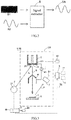
- FIG. 1 is a schematic view illustrating the sample inspection device 1A according to the first embodiment.
- FIG. 2 is a schematic view illustrating a manner in which a signal having a frequency corresponding to a frequency of a reference signal S2 is extracted from within a detection signal S1.
- the sample inspection device 1A is provided with a light source 2, a photocathode 3, a detector 7, and a signal extractor 8.
- the light source 2 is a light source for emitting frequency-modulated light, a frequency of which is modulated.
- the light source 2 is a pulse light source for emitting pulse light, which is a type of frequency-modulated light.
- the light source 2 may be a light source for emitting frequency-modulated light other than pulse light (e.g., a light source for emitting frequency-modulated light, an intensity of which varies sinusoidally).
- pulse light shall be replaced with "frequency-modulated light” in the description below.
- the term "frequency-modulated light” in the present specification means light having a periodically varying intensity.
- pulse light in the present specification means light from among frequency-modulated light in which periods of essentially zero light intensity are periodically present.
- the light source 2 is a light source for emitting pulse light L. From the perspective of obtaining high-intensity pulse light, the light source 2 is preferably a laser light source for emitting pulse light L.
- the light source 2 is a light source for emitting a high-output (watt-class), high-frequency (several hundred MHz), short-pulse (several hundred femtoseconds) laser pulse.
- the light source 2 may be a relatively inexpensive laser diode, LED, or the like.
- the light source 2 is disposed outside a vacuum chamber CB. Alternatively, the light source 2 may be disposed inside the vacuum chamber CB.
- any configuration can be adopted for the light source 2.
- a pulse light source using a Q-switch pulse oscillator can be used.
- a voltage is applied to an electro-optic element 21 included in the light source 2, and a Q value of the electro-optic element thereby changes.
- pulse light synchronized with a timing of voltage application is obtained.
- a light source 2 can be used in which a beam output of a continuous laser is turned ON/OFF by a mechanical shutter (including a so-called optical chopper).
- Pulse light may be generated from a continuous laser beam using a liquid crystal shutter, an electro-optic modulator, or an acousto-optic modulator instead of a mechanical shutter.
- a semiconductor laser light source can be used. In this case, pulse light is obtained by turning ON/OFF an electric current supplied to a semiconductor element.
- a pulse light source which utilizes a mode-lock method can be used.
- the photocathode 3 is disposed inside the vacuum chamber CB.
- the photocathode 3 (more specifically, the semiconductor photocathode) emits an electron beam B (more specifically, a pulsed electron beam) in response to reception of the pulse light L emitted by the light source 2. More specifically, electrons in the photocathode 3 are excited by the pulse light, and excited electrons are emitted from the photocathode 3. The emitted electrons are accelerated by an electric field generated by an anode 4 and a cathode (including the photocathode 3), and an electron beam is formed.
- an electron beam B more specifically, a pulsed electron beam
- the pulse light is radiated from a front surface side of the photocathode 3, but the pulse light may alternatively be radiated from a back surface side of the photocathode 3.
- the photocathode 3 is disposed inside a photocathode accommodating vessel 5 provided with an electron beam passage hole 5h.
- a treatment material 5m for EA surface treatment (i.e., treatment for lowering electron affinity) of the photocathode 3 may be disposed inside the photocathode accommodating vessel 5.
- the photocathode material for forming the photocathode 3 there are no particular limitations as to the photocathode material for forming the photocathode 3, and there may be cited, for example, Group III-V semiconductor materials and Group II-VI semiconductor materials. Specifically, AlN, Ce 2 Te, GaN, K 2 CsSb, AlAs, GaP, GaAs, GaSb, InAs, and the like, and mixed crystals thereof and the like may be cited. Metals may be cited as another example. Specifically, Mg, Cu, Nb, LaB 6 , SeB 6 , Ag, and the like may be cited.
- the photocathode 3 can be fabricated through EA surface treatment of said photocathode material, and through selection of the structure and material of the semiconductor material for the photocathode 3, it is possible not only to select the electron-excitation light from within a near-ultraviolet to infrared wavelength region depending on the gap energy of the semiconductor, but also to select the electron-beam source capabilities (quantum yield, durability, monochromaticity, temporal response, and spin polarization) depending on the electron beam application.
- An electron beam B emitted from the photocathode 3 is incident on a sample T.
- the sample T is supported by a sample stage 6.
- the sample T is a wafer, an integrated circuit, NAND-type flash memory, DRAM, or an intermediate product (semi-finished product) thereof, or any electronic material or the like.
- the sample T may be a battery material, an LED, an LD, a biological sample, organic matter, or another sample susceptible to damage by electron ray irradiation.
- the sample T and the sample stage 6 are disposed inside the vacuum chamber CB.
- Reflected electrons, secondary electrons, transmitted electrons, and other electrons are emitted from the sample T irradiated by the electron beam B.
- the reflected electrons are electrons that are reflected by the sample T from among the electrons in the electron beam B.
- the secondary electrons are electrons emitted from inside the sample T due to irradiation of the sample T by the electron beam B.
- the transmitted electrons are electrons that are transmitted through the sample T from among the electrons in the electron beam B.
- the detector 7 detects electrons e such as reflected electrons and secondary electrons emitted from the sample, or transmitted electrons, and generates a detection signal S1.
- the detector 7 may be a scintillator, a microchannel plate, or any other electron detector, for example.
- the detector 7 is disposed inside the vacuum chamber CB.
- a configuration may also be adopted in which an electron detection part of the detector 7 is disposed inside the vacuum chamber CB and any constituent elements other than the electron detection part of the detector 7 are disposed outside the vacuum chamber.
- the signal extractor 8 extracts a signal having a frequency corresponding to the pulse frequency of the pulse light L (pulse light emitted from the light source 2) from within a detection signal S1 generated by the detector 7. For example, the signal extractor 8 receives a detection signal S1 from the detector 7, and receives a signal (reference signal S2) corresponding to a pulse waveform of the pulse light from the light source 2. The signal extractor 8 extracts a signal having a frequency corresponding to the frequency of the abovementioned reference signal S2 from the detection signal S1 received from the detector 7.
- pulse frequency shall be replaced with “modulation frequency” (i.e., the frequency of the change in intensity of the frequency-modulated light). Pulse frequency is also a type of modulation frequency.
- a publicly known lock-in amplifier for example, can be used as the signal extractor 8.
- the lock-in amplifier receives the detection signal S1 and the reference signal S2, and extracts a signal having a frequency corresponding to the frequency of the reference signal S2 from the detection signal S1.
- any electronic circuit e.g., a frequency filter
- a computer may be used as the signal extractor 8. In this case, the computer extracts a signal having a frequency corresponding to the frequency of the reference signal from within the detection signal using any computer program for extracting a specific frequency component from a signal which includes noise.
- signal data corresponding to the detection signal generated by the detector 7, and frequency data corresponding to the frequency of the reference signal are inputted to the computer, and the computer converts the abovementioned signal data to data in which a frequency component corresponding to the frequency of the reference signal is emphasized using the abovementioned computer program, and outputs the resultant data.
- a control signal (e.g., a voltage signal inputted to the electro-optic element 21 of the light source, a drive signal for driving the mechanical shutter of the light source, an ON/OFF signal inputted to the semiconductor laser, or the like) for causing the light source 2 to operate has the same frequency as the pulse frequency of the pulse light.
- the control signal for causing the light source 2 to operate can therefore be used as the reference signal inputted to the signal extractor 8.
- a laser light source using a passive Q-switch, a laser light source using a mode-lock method, or the like is used as the light source 2, there is no need to send a control signal for frequency modulation to the light source 2.
- a portion of the pulse light emitted from the light source 2 may be received by a photodiode, and an electrical signal generated by this light reception may be used as a reference signal to be inputted to the signal extractor 8.
- a signal having a frequency corresponding to the pulse frequency of the pulse light L in the detection signal S1 is a signal generated as a result of reception of the pulsed electron beam B by the sample T.
- a signal having a frequency corresponding to the pulse frequency of the pulse light L can be considered to be a signal indicating a state (structure, shape, material, etc.) of a region (region of the sample T) irradiated by the pulsed electron beam, and can be considered to be a signal from which noise is removed.
- the first embodiment there is no need to dispose a blanking electrode and a blanking slit between the photocathode 3 and the sample T.
- the electron beam emitted from the photocathode 3 is therefore effectively utilized.
- the drawback arises that there is a significant decrease in the amount of electrons from before to after passage thereof through the blanking slit.
- the problem also arises that misalignment occurs at the irradiation position of the electron beam as the blanking electrode is controlled at high speed.
- sample inspection device 1A synergistically exhibits the three effects described below.
- a first effect is that by radiating an electron beam B to the sample T to inspect the sample, a diameter of an inspection spot can be reduced in size relative to a case in which the sample is inspected by light irradiation.
- the state (structure, shape, material, etc.) of a more minute region can be inspected.
- a second effect is that through use of the photocathode 3 as the electron beam source, a high-intensity electron beam B can be generated.
- a high-intensity electron beam can be generated, and minute defects and the like in the sample T can therefore be detected even when a scanning speed is increased.
- a spot diameter of the electron beam is decreased in size to inspect a minute region, the time taken to scan the sample T using the electron beam increases.
- the photocathode 3 is used as the electron beam source, the intensity of the electron beam is increased by at least several times (e.g., at least 10 times) relative to a case in which another electron beam source is used.
- a sample can therefore be inspected in a shorter time despite the small spot diameter of the electron beam.
- a semiconductor photocathode has higher quantum efficiency than a metal photocathode, and adequate excitation is therefore obtained even by light having a relatively low peak power, as in the case of a semiconductor laser (or an LED).
- a degree of freedom in selection of a unit waveform of the frequency-modulated light radiated to the photocathode 3 is therefore increased when a semiconductor photocathode is used as the photocathode 3.
- noise removal characteristics of the signal extractor 8 are enhanced relative to a case in which pulse light having a rectangular waveform is used.
- a semiconductor laser or an LED
- the modulation frequency of the frequency-modulated light can be freely selected. Therefore, by employing a frequency different from a known noise frequency as the modulation frequency of the frequency-modulated light emitted from the light source 2, the noise removal characteristics of the signal extractor 8 (e.g., the lock-in amplifier) can be further enhanced.
- a mode-lock laser or a passive Q-switch laser is used as the light source 2, it is difficult to freely select the modulation frequency of the frequency-modulated light.
- a third effect is that by extracting a signal having a frequency corresponding to the pulse frequency of the pulse light L from within the detection signal generated by the detector 7, a noise component included in the detection signal can be effectively removed.
- a time of inspection time of electron beam irradiation
- the first embodiment is provided with the signal extractor 8 for extracting a signal having a frequency corresponding to the pulse frequency of the pulse light from within the detection signal S1. Therefore, even when a signal indicating a state (structure, shape, material, etc.) of the sample is faint relative to noise, the signal indicating a state of the sample can be effectively extracted from within the noise. There is thereby no need to increase the time of inspection at each inspection spot to enhance the S/N ratio of the detection signal, and the electron beam scanning speed can be increased.
- the problem caused by the small spot diameter of the electron beam is solved by the synergistic effect of enhancing electron beam intensity through use of the photocathode 3 and reducing noise through use of the signal extractor 8, which are innovative ways of enabling increased speed of sample inspection.
- the S/N ratio decreases due to such effects as decreased efficiency of generation of secondary electrons emitted from the sample T.
- the problem of decreased S/N ratio can be overcome by extracting a signal having a frequency corresponding to the frequency of the pulse light from within a detection signal having a low S/N ratio.
- the sample inspection device 1A according to the first embodiment is used, high-precision inspection is possible even for a sample which was difficult to inspect conventionally via an electron beam B, i.e., a sample which is susceptible to damage by an electron beam.
- the pulse frequency of the pulse light L emitted from the light source 2 is preferably 50 MHz or greater, 100 MHz or greater, or 150 MHz or greater, for example.
- a high pulse frequency By adopting a high pulse frequency, a large number of pulsed electron beams can be radiated to the sample in a short time.
- the signal extractor 8 it is possible for the signal extractor 8 to extract a signal having a frequency corresponding to the frequency of the reference signal S2 from a detection signal S1 acquired in a short time.
- the modulation frequency is also preferably 50 MHz or greater, 100 MHz or greater, or 150 MHz or greater.
- the sample inspection device 1A may be a device for detecting a defect in a sample, or a microscope for visualizing a fine structure of a sample.
- FIG. 3 is a schematic view illustrating the sample inspection device 1B according to the second embodiment.
- FIG. 4A is a diagram for describing a pulse amplitude PA, a pulse width PW, and a pulse interval PI.
- FIG. 4B is a diagram for describing an amplitude ZA of the frequency-modulated light, and a time interval ZW between two maximum amplitudes of the frequency-modulated light.
- FIG. 5 is a schematic view illustrating the manner in which a sample type and a plurality of control parameter values are associated and stored.
- FIG. 6 is a schematic view illustrating the manner in which a light source control device 9 can selectively execute a first control mode for varying a light quantity per unit time of the pulse light L emitted from the light source 2, and a second control mode for holding constant the light quantity per unit time of pulse light emitted from the light source 2.
- FIG. 7 is a schematic view of an example of the sample inspection device 1B according to the second embodiment.
- the sample inspection device 1B according to the second embodiment is provided with a light source 2, a photocathode 3, a detector 7, and a signal extractor 8.
- the sample inspection device 1B according to the second embodiment may be provided with at least one of a vacuum chamber CB, an anode 4, a photocathode accommodating vessel 5, and a sample stage 6.
- the light source 2, photocathode 3, anode 4, photocathode accommodating vessel 5, sample stage 6, detector 7, signal extractor 8, and vacuum chamber CB in the second embodiment are the same as the light source 2, photocathode 3, anode 4, photocathode accommodating vessel 5, sample stage 6, detector 7, signal extractor 8, and vacuum chamber CB in the first embodiment, and repeated description of the structure thereof is therefore omitted.
- the sample inspection device 1B is provided with a light source control device 9 for controlling operation of the light source 2.
- the light source control device 9 controls the light source 2 in accordance with a control parameter value.
- the control parameter value includes at least one of a pulse amplitude control parameter value, a pulse width control parameter value, a parameter value for prescribing a unit pulse waveform (e.g., a parameter value for prescribing a rectangular wave, a sine wave, a sawtooth wave, a Gaussian waveform, or the like), and a pulse interval control parameter value.
- the control parameter value may include at least two, three, or all of a pulse amplitude control parameter value, a pulse width control parameter value, a parameter value for prescribing a pulse waveform, and a pulse interval control parameter value. As indicated in FIG.
- the pulse amplitude PA means the maximum value of the intensity of the pulse light
- the pulse width PW means an ON time (i.e., the duration of a luminescent state of the pulse light) of a pulse
- the pulse interval PI means an OFF time (i.e., the duration of a non-luminescent state of the pulse light) of a pulse.
- the "pulse amplitude control parameter value,” the “pulse width control parameter value,” and the “parameter value for prescribing a unit pulse waveform” shall be replaced with “frequency-modulated light amplitude control parameter value,” “control parameter value for prescribing the time interval between two maximum amplitudes of the frequency-modulated light,” and “parameter value for prescribing a unit waveform of the frequency-modulated light,” respectively.
- An example of the “amplitude (ZA) of the frequency-modulated light” and the “time interval (ZW) between two maximum amplitudes of the frequency-modulated light” is presented in FIG. 4B .
- the light source control device 9 controls the light source 2 in accordance with the pulse amplitude control parameter value, and the light source 2 thereby emits pulse light having a desired pulse amplitude.
- the light source control device 9 also controls the light source 2 in accordance with the pulse width control parameter value, and the light source 2 thereby emits pulse light having a desired pulse width.
- the light source control device 9 also controls the light source 2 in accordance with the pulse interval control parameter value, and the light source 2 thereby emits pulse light having a desired pulse interval.
- the waveform e.g., the pulse amplitude, pulse width, pulse interval, unit pulse waveform, and pulse frequency
- the waveform e.g., the pulse amplitude, pulse width, pulse interval, unit pulse waveform, and pulse frequency
- the sample inspection device 1B is provided with a storage device M (ROM, RAM, hard disk, or the like) for storing first associated data DA in which the type of sample T and a control parameter value are associated.
- the storage device M associates and stores a first sample T1 and a plurality of control parameter values. More specifically, the storage device M associates and stores the first sample T1, a pulse amplitude control parameter value VA1, a pulse width control parameter value VW1, and a pulse interval control parameter value VI1.
- a storage device M ROM, RAM, hard disk, or the like
- the storage device M associates and stores a second sample T2 and a plurality of control parameter values. More specifically, the storage device M associates and stores the second sample T2, a pulse amplitude control parameter value VA2, a pulse width control parameter value VW2, and a pulse interval control parameter value VI2.
- the pulse amplitude control parameter value VA1 stored by the storage device M should be made smaller than the pulse amplitude control parameter value VA2 stored by the storage device M.
- the pulse width control parameter value VW1 stored by the storage device M should be made smaller than the pulse width control parameter value VW2 stored by the storage device M.
- a weaker pulse light and a weaker electron beam
- a stronger pulse light and a stronger electron beam
- the pulse width control parameter value VW1 stored by the storage device M should be made smaller than the pulse width control parameter value VW2 stored by the storage device M.
- the pulse interval control parameter value VI1 stored by the storage device M should be made larger than the pulse interval control parameter value VI2 stored by the storage device M. In this case, accumulation of heat in the sample is more suppressed during inspection of the first sample T1 than during inspection of the second sample T2.
- the sample inspection device 1B is preferably provided with an input device 91 for receiving inputting of the sample type.
- the light source control device 9 extracts a control parameter value corresponding to the inputted sample type on the basis of the first associated data stored in the storage device M. The light source control device 9 then controls operation of the light source 2 using the extracted control parameter value.
- the type of sample T may be automatically specified.
- the sample inspection device 1B is provided with a camera or other sample recognition device for specifying the sample type.
- the light source control device 9 extracts a control parameter value corresponding to the specified sample type on the basis of information relating to the sample type specified by the sample recognition device and the first associated data stored in the storage device M.
- the light source control device 9 then controls operation of the light source 2 using the extracted control parameter value.
- the light source control device 9 can selectively execute a first control mode for varying a light quantity per unit time of the pulse light L emitted from the light source 2, and a second control mode for holding constant the light quantity per unit time of pulse light emitted from the light source 2.
- durability of the sample T to the electron beam B can be inspected.
- a sample of the sample T for example, is used.
- the light quantity per unit time of the pulse light is gradually increased.
- the light quantity per unit time of the pulse light is increased until the sample T is damaged by the electron beam B.
- the presence/absence of damage to the sample T is determined by image analysis, for example.
- the sample T is not damaged when the light quantity per unit time of the pulse light is equal to or less than a first threshold value Th1, and the sample T is damaged when the light quantity per unit time of the pulse light is greater than a second threshold value Th2.
- the light quantity per unit time of the pulse light is set so as to be equal to or less than the first threshold value Th1.
- the first threshold value Th1 and the second threshold value Th2 may be the same value, but when there is a range in which the presence/absence of damage to the sample T is unclear, the first threshold value Th1 and the second threshold value Th2 may be different values, respectively.
- a sample e.g., an actual product
- a sample T can be inspected without damaging the sample T.
- the light quantity per unit time of the pulse light is held constant. From the perspective of suppressing damage to the sample T, the light quantity per unit time of the pulse light in the second control mode is maintained so as to be equal to or less than the first threshold value Th1.
- the light quantity per unit time of the pulse light is gradually increased in the first control mode.
- the light quantity per unit time of the pulse light may be gradually decreased in the first control mode.
- the waveform of the pulse light when the waveform of the pulse light can be adjusted, it is then possible to select a more appropriate pulse waveform for a characteristic of the sample. For example, by selecting the maximum intensity in a range in which the sample is not damaged by the intensity of the pulse light (e.g., the intensity of the electron beam), the speed of inspection of the sample T can be increased.
- the maximum intensity in a range in which the sample is not damaged by the intensity of the pulse light e.g., the intensity of the electron beam
- the sample inspection device 1B is provided with a power source 40 for applying a voltage between the anode 4 and the photocathode 3 (more specifically, a cathode including the photocathode 3), and a voltage control device 42 for controlling a magnitude of the voltage applied between the anode 4 and the photocathode 3.
- a power source 40 for applying a voltage between the anode 4 and the photocathode 3 (more specifically, a cathode including the photocathode 3)
- a voltage control device 42 for controlling a magnitude of the voltage applied between the anode 4 and the photocathode 3.
- the electron beam B can reach a deeper region of the sample T. In other words, inspection of the sample T can extend to a deeper region thereof. Meanwhile, when the voltage applied between the anode 4 and the photocathode 3 is small, a surface portion of a sample can be prioritized for inspection.
- Example of a mechanism of sample scanning by the electron beam B is described below with reference to FIG. 7 .
- the sample inspection device 1B may be provided with a drive device 61 for moving the sample stage 6.
- the sample stage 6 is moved, and the sample T is thereby scanned by the electron beam B.
- a direction in which the sample stage 6 is moved by the drive device 61 is parallel to an inspection surface of the sample T, for example.
- the sample inspection device 1B may be provided with a drive device 31 for moving the photocathode 3.
- the photocathode 3 is moved, and the sample T is thereby scanned by the electron beam B.
- a direction in which the photocathode 3 is moved by the drive device 31 is parallel to the inspection surface of the sample T, for example.
- the sample inspection device 1B may be provided with an electron beam deflection device 33 for bending the electron beam emitted from the photocathode 3.
- the electron beam B emitted from the photocathode 3 is deflected, and the sample T is thereby scanned by the electron beam B.
- the electron beam deflection device 33 includes a deflecting electrode for generating an electric field in a direction intersecting with a direction of travel of the electron beam B, for example.
- the sample inspection device 1B may be provided with a storage device 11 for recording the signal extracted by the signal extractor 8, and/or a display device 12 for visually displaying the signal extracted by the signal extractor 8.
- the storage device 11 may be configured to associate and record a position of irradiation in the sample T by the electron beam B and the signal extracted by the signal extractor 8. In this case, by referring to a relationship between the irradiation position and the intensity of the signal extracted by the signal extractor 8, the position of a defect in the sample T can be identified.
- the display device 12 may also associate and display the position of irradiation in the sample T by the electron beam B and the signal extracted by the signal extractor 8.
- FIG. 8 is a flowchart illustrating an example of the sample inspection method according to an embodiment of the present invention.
- the sample inspection method according to an embodiment of the present invention may be executed using the sample inspection device 1A of the first embodiment or the sample inspection device 1B of the second embodiment, or executed using another sample inspection device.
- a first step ST1 the pulse light L is radiated to the photocathode 3.
- the first step ST1 is a pulse light irradiation step.
- the pulse frequency of the pulse light L may be modified prior to the first step ST1 in accordance with the type of the sample T to be inspected.
- the pulse frequency of the pulse light may be set to a first frequency F1 when the sample T is the first sample T1
- the pulse frequency of the pulse light may be set to a second frequency F2 different from the first frequency when the sample T is the second sample T2.
- the control parameter value (e.g., at least one control parameter value from among the pulse amplitude control parameter value, the pulse width control parameter value, the parameter value for prescribing a unit pulse waveform, and the pulse interval control parameter value) for controlling operation of the light source 2 may also be modified prior to the first step ST1 in accordance with the type of the sample T to be inspected.
- the pulse amplitude control parameter value, the pulse width control parameter value, and the pulse interval control parameter value may be set to a value VA1, a value VW1, and a value VI1, respectively
- the pulse amplitude control parameter value, the pulse width control parameter value, and the pulse interval control parameter value may be set to a value VA2, a value VW2, and a value VI2, respectively.
- the voltage applied between the anode 4 and the photocathode 3 may also be modified prior to the first step ST1 in accordance with the type of the sample T to be inspected.
- the voltage applied between the anode 4 and the photocathode 3 may be set to a voltage V1
- the voltage applied between the anode 4 and the photocathode 3 may be set to a voltage V2 different from the voltage V1.
- a second step ST2 the electron beam B emitted from the photocathode 3 is radiated to the sample T.
- the second step ST2 is an electron beam irradiation step.
- Emission of the electron beam B from the photocathode 3 in the second step ST2 is a phenomenon caused by irradiation of the photocathode 3 by the pulse light. Therefore, when the pulse frequency of the pulse light radiated to the photocathode 3 is the first frequency F1, the electron beam B is a pulsed electron beam in which a frequency of variation in the amount of electrons thereof is the first frequency F1.
- a third step ST3 reflected electrons and secondary electrons emitted from the sample T, or transmitted electrons, are detected by the detector 7.
- the third step ST3 is a detection step for detecting electrons.
- the detector 7 is disposed on the same side of the sample T as the photocathode 3.
- the detector 7 is disposed on the opposite side of the sample T from the photocathode 3.
- Emission of electrons (reflected electrons and secondary electrons, or transmitted electrons) from the sample T in the third step ST3 is a phenomenon caused by irradiation of the sample T by the electron beam B. Therefore, when the pulse frequency of variation in the amount of electrons in the electron beam B radiated to the sample T is the first frequency F1, a signal SA (see FIG. 2 ) having the first frequency F1 in the detection signal generated by the detector 7 can be considered to be a signal (non-noise signal) generated as a result of irradiation by the electron beam B.
- a signal having a frequency corresponding to the pulse frequency of the pulse light L is extracted from within the detection signal generated by the detector 7.
- the fourth step ST4 is a signal extraction step.
- Signal extraction in the fourth step ST4 is performed using a lock-in amplifier or other signal extractor 8. More specifically, when the pulse frequency of the pulse light emitted by the light source 2 is the first frequency F1, a signal SA having the first frequency F1 is extracted from within the detection signal S1 generated by the detector 7, for example.
- a sample inspection step is constituted from the pulse light irradiation step, the electron beam irradiation step, the detection step, and the signal extraction step described above.
- a durability inspection step for inspecting durability of the sample T or a sample of the same type as the sample T may be performed prior to the sample inspection step.
- the sample T (or a sample T' of the same type as the sample T) is inspected for durability to an electron beam.
- the durability inspection step the light quantity per unit time of the pulse light emitted from the light source 2 is varied. A relationship between the light quantity per unit time of the pulse light L emitted from the light source 2 and damage to the sample T (or the sample T' of the same type as the sample T) is determined. This relationship is, for example that the sample T (or the sample T' of the same type as the sample T) is not damaged when the light quantity per unit time of the pulse light is equal to or less than a first threshold value Th1, and the sample T (or the sample T' of the same type as the sample T) is damaged when the light quantity per unit time of the pulse light is greater than a second threshold value Th2.
- a control parameter value for the light source 2 to be used in the sample inspection step is determined in accordance with an inspection result of the durability inspection step. For example, a control parameter value (pulse amplitude control parameter value, pulse width control parameter value, pulse interval control parameter value, etc.) is determined so that the light quantity per unit time of the pulse light emitted from the light source 2 is equal to or less than the first threshold value Th1. Control parameters are preferably determined so that the light quantity per unit time of the pulse light emitted from the light source 2 is equal to or less than the first threshold value Th1 and is close to the first threshold value Th1.
- a control parameter value pulse amplitude control parameter value, pulse width control parameter value, pulse interval control parameter value, etc.
- the intensity of the electron beam radiated to the sample can be optimized in accordance with the durability of the sample.
- a method for inspecting a sample T that is a layered body will be described with reference to FIG. 9 .
- a first layer LA1 of the sample T is inspected, and a second layer LA2 layered on the first layer LA1 is subsequently inspected.
- a first layer inspection step for inspecting the first layer LA1 of the sample T includes the pulse light irradiation step, the electron beam irradiation step, the detection step, and the signal extraction step described above.
- the electron beam B is radiated to the first layer LA1.
- the second layer LA2 is layered over the first layer LA1.
- the first layer LA1 is thereby covered by the second layer LA2.
- the second layer LA2 is layered directly on the first layer LA1 in the example illustrated in FIG. 9 , but the second layer LA2 may also be layered on the first layer LA1 on top of another layer.
- a second layer inspection step for inspecting the second layer LA2 of the sample T includes the pulse light irradiation step, the electron beam irradiation step, the detection step, and the signal extraction step described above.
- the electron beam B is radiated to the second layer LA2 so that the electron beam B does not reach the first layer LA1; in other words, so that the electron beam B essentially does not reach the first layer LA1.
- the voltage applied between the anode 4 and the photocathode 3 (more specifically, the cathode including the photocathode 3) is set, for example, so that the electron beam B does not reach the first layer LA1.
- a focus or other characteristic of an electron lens system may be set so that the electron beam B does not reach the first layer LA1.
- the present invention is not limited to the embodiments described above, and it is clear that the embodiments can be appropriately modified or changed within the range of the technical idea of the present invention. Any of the constituent elements used in the embodiments can also be incorporated into another embodiment, and any of the constituent elements of the embodiments can also be omitted.
- an electron beam is radiated to a sample using a single light source 2 and a single photocathode 3.
- frequency-modulated light having a first frequency is radiated from a first light source to a first photocathode, and a first electron beam is radiated from the first photocathode to a first portion of a sample.
- frequency-modulated light having a second frequency is radiated from a second light source to a second photocathode, and a second electron beam is radiated from the second photocathode to a second portion of the sample.
- Electrons reflected by the first portion (or transmitted through the first portion) are then received by the detector 7, and electrons reflected by the second portion (or transmitted through the second portion) are received by the detector 7.
- a detection signal corresponding to the first frequency and a detection signal corresponding to the second frequency are subsequently extracted by the signal extractor 8. In this manner, the first portion and the second portion can be inspected simultaneously. Through simultaneous inspection of a first portion and a second portion, the time taken to inspect a sample can be shortened.
- a configuration may be adopted in which the frequency of the frequency-modulated light is not varied for each light source 2; for example, the frequency of the frequency-modulated light radiated from first and second light sources 2 may be the same.
- the number of detectors 7 provided should be the same as the number of light sources 2.
- a set comprising a single photocathode 3 and a plurality of light sources 2 may be prepared.
- the photocathode 3 receives frequency-modulated light radiated from the light sources 2, the photocathode 3 can emit an electron beam B. Consequently, by causing the photocathode 3 for receiving the frequency-modulated light radiated from the plurality of light sources 2 to have different regions, despite there being a single photocathode 3, the same effect is obtained as in the abovementioned example in which a plurality of sets comprising a light source 2 and a photocathode 3 are prepared.
- a plurality of sets of a single photocathode 3 and a plurality of light sources 2 may also be prepared.
- the sample inspection device and sample inspection method of the present invention Through use of the sample inspection device and sample inspection method of the present invention, noise is removed from a detection signal, and a generated electron beam is utilized effectively for inspection.
- the present invention is therefore useful to a manufacturer of a sample inspection device, and to an inspector of a sample using the sample inspection device and the sample inspection method.
Landscapes
- Chemical & Material Sciences (AREA)
- Analytical Chemistry (AREA)
- General Health & Medical Sciences (AREA)
- Life Sciences & Earth Sciences (AREA)
- Health & Medical Sciences (AREA)
- Biochemistry (AREA)
- Physics & Mathematics (AREA)
- General Physics & Mathematics (AREA)
- Immunology (AREA)
- Pathology (AREA)
- Crystallography & Structural Chemistry (AREA)
- Analysing Materials By The Use Of Radiation (AREA)
- Electron Sources, Ion Sources (AREA)
Applications Claiming Priority (2)
| Application Number | Priority Date | Filing Date | Title |
|---|---|---|---|
| JP2017252709 | 2017-12-27 | ||
| PCT/JP2018/046926 WO2019131410A1 (ja) | 2017-12-27 | 2018-12-20 | 試料検査装置、および、試料検査方法 |
Publications (2)
| Publication Number | Publication Date |
|---|---|
| EP3734641A1 true EP3734641A1 (de) | 2020-11-04 |
| EP3734641A4 EP3734641A4 (de) | 2021-04-07 |
Family
ID=67063623
Family Applications (1)
| Application Number | Title | Priority Date | Filing Date |
|---|---|---|---|
| EP18897698.9A Withdrawn EP3734641A4 (de) | 2017-12-27 | 2018-12-20 | Probeninspektionsvorrichtung und probeninspektionsverfahren |
Country Status (8)
| Country | Link |
|---|---|
| US (1) | US11150204B2 (de) |
| EP (1) | EP3734641A4 (de) |
| JP (1) | JP6604649B1 (de) |
| KR (1) | KR102238479B1 (de) |
| CN (1) | CN110582833B (de) |
| IL (1) | IL270143B2 (de) |
| TW (1) | TWI794375B (de) |
| WO (1) | WO2019131410A1 (de) |
Cited By (2)
| Publication number | Priority date | Publication date | Assignee | Title |
|---|---|---|---|---|
| EP4310883A4 (de) * | 2021-05-26 | 2024-08-28 | Photo Electron Soul Inc. | Elektronenkanone, elektronenstrahlapplikationsvorrichtung und elektronenstrahlemissionsverfahren |
| EP4401109A4 (de) * | 2021-09-07 | 2025-06-25 | Photo Electron Soul Inc. | Verfahren zur erzeugung von erkennungsdaten in einer elektronenstrahlanwendung, verfahren zur bildsynthese eines objekts, programm, aufzeichnungsmedium und elektronenstrahlanwendung |
Families Citing this family (8)
| Publication number | Priority date | Publication date | Assignee | Title |
|---|---|---|---|---|
| US12165828B2 (en) * | 2019-10-31 | 2024-12-10 | Hitachi High-Tech Corporation | Electron gun and electron beam application apparatus |
| JP6722958B1 (ja) | 2019-11-20 | 2020-07-15 | 株式会社Photo electron Soul | 電子線適用装置および電子線適用装置における電子ビームの射出方法 |
| CN110890256B (zh) * | 2019-11-26 | 2021-07-27 | 华中科技大学 | 一种会聚角可调无磁飞秒电子源装置 |
| US11933668B2 (en) * | 2020-02-03 | 2024-03-19 | Rohde & Schwarz Gmbh & Co. Kg | Sampling assembly and testing instrument |
| KR102790213B1 (ko) | 2020-04-20 | 2025-04-03 | 에이에스엠엘 네델란즈 비.브이. | 검사 도구 및 검사 도구 작동 방법 |
| WO2022091234A1 (ja) * | 2020-10-28 | 2022-05-05 | 株式会社日立ハイテク | 荷電粒子ビーム装置および試料観察方法 |
| JP7054281B1 (ja) * | 2021-10-19 | 2022-04-13 | 株式会社Photo electron Soul | 電子線適用装置および電子線適用装置における検出データの作成方法 |
| CN117928722B (zh) * | 2023-12-08 | 2024-11-05 | 江苏省环境监测中心 | 基于自主网的噪声监测装置及噪声溯源优化方法 |
Family Cites Families (27)
| Publication number | Priority date | Publication date | Assignee | Title |
|---|---|---|---|---|
| US3908193A (en) * | 1972-11-27 | 1975-09-23 | Albert Macovski | Color television encoding and decoding system |
| JPS61184445A (ja) | 1985-02-12 | 1986-08-18 | Shimadzu Corp | X線光電子分光装置 |
| JPH0754687B2 (ja) * | 1987-04-24 | 1995-06-07 | 株式会社日立製作所 | パターン検査方法およびその装置 |
| JPS6475928A (en) * | 1987-09-17 | 1989-03-22 | Hamamatsu Photonics Kk | Optical heterodyne detector |
| DE3738453A1 (de) | 1987-11-12 | 1989-08-03 | Brust Hans Detlef | Verfahren und anordnung zur messung des signalverlaufs an einem messpunkt einer probe |
| DE3839707A1 (de) * | 1988-11-24 | 1990-05-31 | Integrated Circuit Testing | Verfahren zum betrieb eines elektronenstrahlmessgeraetes |
| JP2709135B2 (ja) * | 1989-04-11 | 1998-02-04 | 浜松ホトニクス株式会社 | 光信号検出装置 |
| DE3917411A1 (de) * | 1989-05-29 | 1990-12-06 | Brust Hans Detlef | Verfahren und anordnung zur schnellen spektralanalyse eines signals an einem oder mehreren messpunkten |
| US5179565A (en) * | 1990-06-07 | 1993-01-12 | Hamamatsu Photonics, K.K. | Low noise pulsed light source utilizing laser diode and voltage detector device utilizing same low noise pulsed light source |
| US5270780A (en) * | 1991-09-13 | 1993-12-14 | Science Applications International Corporation | Dual detector lidar system and method |
| US5684360A (en) | 1995-07-10 | 1997-11-04 | Intevac, Inc. | Electron sources utilizing negative electron affinity photocathodes with ultra-small emission areas |
| JPH09298032A (ja) * | 1996-04-30 | 1997-11-18 | Hamamatsu Photonics Kk | 電子ビーム発生装置 |
| JPH10334842A (ja) * | 1997-05-28 | 1998-12-18 | Shimadzu Corp | 光走査型電子顕微鏡 |
| US6724002B2 (en) * | 2001-01-31 | 2004-04-20 | Applied Materials, Inc. | Multiple electron beam lithography system with multiple beam modulated laser illumination |
| US20030048427A1 (en) * | 2001-01-31 | 2003-03-13 | Applied Materials, Inc. | Electron beam lithography system having improved electron gun |
| JP2002313273A (ja) * | 2001-04-17 | 2002-10-25 | Hitachi Ltd | 電子顕微鏡装置 |
| US6946655B2 (en) * | 2001-11-07 | 2005-09-20 | Applied Materials, Inc. | Spot grid array electron imaging system |
| JP2003303565A (ja) | 2002-04-10 | 2003-10-24 | Hitachi High-Technologies Corp | 電子線検査装置 |
| US7446474B2 (en) * | 2002-10-10 | 2008-11-04 | Applied Materials, Inc. | Hetero-junction electron emitter with Group III nitride and activated alkali halide |
| US6812461B1 (en) * | 2002-11-07 | 2004-11-02 | Kla-Tencor Technologies Corporation | Photocathode source for e-beam inspection or review |
| US7068363B2 (en) * | 2003-06-06 | 2006-06-27 | Kla-Tencor Technologies Corp. | Systems for inspection of patterned or unpatterned wafers and other specimen |
| JP4443167B2 (ja) * | 2003-08-25 | 2010-03-31 | 株式会社日立製作所 | 走査型電子顕微鏡 |
| US7250618B2 (en) * | 2005-02-02 | 2007-07-31 | Nikon Corporation | Radiantly heated cathode for an electron gun and heating assembly |
| JP5102580B2 (ja) | 2007-10-18 | 2012-12-19 | 株式会社日立ハイテクノロジーズ | 荷電粒子線応用装置 |
| JP5610399B2 (ja) * | 2011-08-02 | 2014-10-22 | 独立行政法人科学技術振興機構 | ポンププローブ測定装置 |
| JP6166032B2 (ja) * | 2012-11-06 | 2017-07-19 | 浜松ホトニクス株式会社 | 半導体デバイス検査装置及び半導体デバイス検査方法 |
| JP6568646B2 (ja) | 2016-03-29 | 2019-08-28 | 株式会社日立ハイテクノロジーズ | 電子顕微鏡 |
-
2018
- 2018-12-20 CN CN201880028185.3A patent/CN110582833B/zh active Active
- 2018-12-20 JP JP2019531344A patent/JP6604649B1/ja active Active
- 2018-12-20 US US16/609,728 patent/US11150204B2/en active Active
- 2018-12-20 KR KR1020197031879A patent/KR102238479B1/ko active Active
- 2018-12-20 WO PCT/JP2018/046926 patent/WO2019131410A1/ja not_active Ceased
- 2018-12-20 EP EP18897698.9A patent/EP3734641A4/de not_active Withdrawn
- 2018-12-20 IL IL270143A patent/IL270143B2/en unknown
- 2018-12-21 TW TW107146282A patent/TWI794375B/zh active
Cited By (2)
| Publication number | Priority date | Publication date | Assignee | Title |
|---|---|---|---|---|
| EP4310883A4 (de) * | 2021-05-26 | 2024-08-28 | Photo Electron Soul Inc. | Elektronenkanone, elektronenstrahlapplikationsvorrichtung und elektronenstrahlemissionsverfahren |
| EP4401109A4 (de) * | 2021-09-07 | 2025-06-25 | Photo Electron Soul Inc. | Verfahren zur erzeugung von erkennungsdaten in einer elektronenstrahlanwendung, verfahren zur bildsynthese eines objekts, programm, aufzeichnungsmedium und elektronenstrahlanwendung |
Also Published As
| Publication number | Publication date |
|---|---|
| KR20190133231A (ko) | 2019-12-02 |
| EP3734641A4 (de) | 2021-04-07 |
| KR102238479B1 (ko) | 2021-04-09 |
| US11150204B2 (en) | 2021-10-19 |
| JPWO2019131410A1 (ja) | 2020-01-16 |
| TWI794375B (zh) | 2023-03-01 |
| IL270143A (de) | 2019-12-31 |
| IL270143B2 (en) | 2023-11-01 |
| IL270143B1 (en) | 2023-07-01 |
| US20200080949A1 (en) | 2020-03-12 |
| TW201933411A (zh) | 2019-08-16 |
| CN110582833A (zh) | 2019-12-17 |
| CN110582833B (zh) | 2022-07-01 |
| JP6604649B1 (ja) | 2019-11-13 |
| WO2019131410A1 (ja) | 2019-07-04 |
Similar Documents
| Publication | Publication Date | Title |
|---|---|---|
| US11150204B2 (en) | Sample inspection device and sample inspection method | |
| EP1512963B1 (de) | Fluoreszenz-lebensdauerverteilungs-messsystem und messverfahren dafür | |
| JP4631704B2 (ja) | 半導体デバイスの電界分布測定方法と装置 | |
| US12013341B2 (en) | Microscopy method and system | |
| JPH02262038A (ja) | 光波形測定装置 | |
| EP3918400B1 (de) | Bildgebung mit hohem dynamikbereich | |
| JP7054281B1 (ja) | 電子線適用装置および電子線適用装置における検出データの作成方法 | |
| JP6968481B1 (ja) | 電子線適用装置における検出データの作成方法および照射対象の画像合成方法、プログラム、記録媒体、並びに、電子線適用装置 | |
| JP2680398B2 (ja) | 光波形測定装置 | |
| JP7218034B1 (ja) | 局所観察方法、プログラム、記録媒体および電子線適用装置 | |
| JP2656106B2 (ja) | 光波形測定装置 | |
| Dai et al. | Terahertz micrometer-scale imaging based on spintronic emitters | |
| JP2956330B2 (ja) | 荷電粒子線顕微鏡 | |
| JP2025121211A (ja) | 局所観察方法、プログラム、記録媒体および電子線適用装置 | |
| JPH0670615B2 (ja) | 光波形測定装置 |
Legal Events
| Date | Code | Title | Description |
|---|---|---|---|
| STAA | Information on the status of an ep patent application or granted ep patent |
Free format text: STATUS: THE INTERNATIONAL PUBLICATION HAS BEEN MADE |
|
| PUAI | Public reference made under article 153(3) epc to a published international application that has entered the european phase |
Free format text: ORIGINAL CODE: 0009012 |
|
| STAA | Information on the status of an ep patent application or granted ep patent |
Free format text: STATUS: REQUEST FOR EXAMINATION WAS MADE |
|
| 17P | Request for examination filed |
Effective date: 20191024 |
|
| AK | Designated contracting states |
Kind code of ref document: A1 Designated state(s): AL AT BE BG CH CY CZ DE DK EE ES FI FR GB GR HR HU IE IS IT LI LT LU LV MC MK MT NL NO PL PT RO RS SE SI SK SM TR |
|
| AX | Request for extension of the european patent |
Extension state: BA ME |
|
| REG | Reference to a national code |
Ref country code: DE Ref legal event code: R079 Free format text: PREVIOUS MAIN CLASS: H01J0037244000 Ipc: G01N0023225100 |
|
| A4 | Supplementary search report drawn up and despatched |
Effective date: 20210310 |
|
| DAV | Request for validation of the european patent (deleted) | ||
| DAX | Request for extension of the european patent (deleted) | ||
| RIC1 | Information provided on ipc code assigned before grant |
Ipc: H01J 37/073 20060101ALI20210303BHEP Ipc: G01N 23/203 20060101ALI20210303BHEP Ipc: H01J 37/28 20060101ALI20210303BHEP Ipc: G01N 23/2251 20180101AFI20210303BHEP Ipc: H01J 37/244 20060101ALI20210303BHEP Ipc: G01N 23/04 20180101ALI20210303BHEP Ipc: H01J 37/252 20060101ALI20210303BHEP |
|
| STAA | Information on the status of an ep patent application or granted ep patent |
Free format text: STATUS: EXAMINATION IS IN PROGRESS |
|
| 17Q | First examination report despatched |
Effective date: 20230418 |
|
| STAA | Information on the status of an ep patent application or granted ep patent |
Free format text: STATUS: THE APPLICATION IS DEEMED TO BE WITHDRAWN |
|
| 18D | Application deemed to be withdrawn |
Effective date: 20250604 |