EP3722837B1 - Radiation imaging device - Google Patents
Radiation imaging device Download PDFInfo
- Publication number
- EP3722837B1 EP3722837B1 EP19770489.3A EP19770489A EP3722837B1 EP 3722837 B1 EP3722837 B1 EP 3722837B1 EP 19770489 A EP19770489 A EP 19770489A EP 3722837 B1 EP3722837 B1 EP 3722837B1
- Authority
- EP
- European Patent Office
- Prior art keywords
- radiation
- imaging apparatus
- conductor
- communication unit
- radiation imaging
- Prior art date
- Legal status (The legal status is an assumption and is not a legal conclusion. Google has not performed a legal analysis and makes no representation as to the accuracy of the status listed.)
- Active
Links
- 230000005855 radiation Effects 0.000 title claims description 102
- 238000003384 imaging method Methods 0.000 title claims description 101
- 238000004891 communication Methods 0.000 claims description 81
- 239000004020 conductor Substances 0.000 claims description 55
- 239000000463 material Substances 0.000 claims description 28
- 238000001514 detection method Methods 0.000 claims description 9
- 239000011248 coating agent Substances 0.000 claims description 4
- 238000000576 coating method Methods 0.000 claims description 4
- 238000007747 plating Methods 0.000 claims description 3
- 239000002184 metal Substances 0.000 claims 1
- 239000007769 metal material Substances 0.000 description 9
- 230000005540 biological transmission Effects 0.000 description 6
- 238000002834 transmittance Methods 0.000 description 5
- 238000012986 modification Methods 0.000 description 4
- 230000004048 modification Effects 0.000 description 4
- 239000011347 resin Substances 0.000 description 3
- 229920005989 resin Polymers 0.000 description 3
- 239000004065 semiconductor Substances 0.000 description 3
- 238000012546 transfer Methods 0.000 description 3
- 229910000838 Al alloy Inorganic materials 0.000 description 2
- HBBGRARXTFLTSG-UHFFFAOYSA-N Lithium ion Chemical compound [Li+] HBBGRARXTFLTSG-UHFFFAOYSA-N 0.000 description 2
- 229910000861 Mg alloy Inorganic materials 0.000 description 2
- 229910052782 aluminium Inorganic materials 0.000 description 2
- TZCXTZWJZNENPQ-UHFFFAOYSA-L barium sulfate Chemical compound [Ba+2].[O-]S([O-])(=O)=O TZCXTZWJZNENPQ-UHFFFAOYSA-L 0.000 description 2
- 230000008901 benefit Effects 0.000 description 2
- 239000004918 carbon fiber reinforced polymer Substances 0.000 description 2
- 230000000694 effects Effects 0.000 description 2
- 229910001416 lithium ion Inorganic materials 0.000 description 2
- 238000000034 method Methods 0.000 description 2
- 239000000853 adhesive Substances 0.000 description 1
- 230000001070 adhesive effect Effects 0.000 description 1
- XAGFODPZIPBFFR-UHFFFAOYSA-N aluminium Chemical compound [Al] XAGFODPZIPBFFR-UHFFFAOYSA-N 0.000 description 1
- 239000003990 capacitor Substances 0.000 description 1
- 229910052802 copper Inorganic materials 0.000 description 1
- 230000003247 decreasing effect Effects 0.000 description 1
- 238000011161 development Methods 0.000 description 1
- 230000018109 developmental process Effects 0.000 description 1
- 238000006073 displacement reaction Methods 0.000 description 1
- 230000005611 electricity Effects 0.000 description 1
- 239000011888 foil Substances 0.000 description 1
- 239000011521 glass Substances 0.000 description 1
- 230000017525 heat dissipation Effects 0.000 description 1
- 229910052745 lead Inorganic materials 0.000 description 1
- 239000003562 lightweight material Substances 0.000 description 1
- 230000000873 masking effect Effects 0.000 description 1
- 229910052750 molybdenum Inorganic materials 0.000 description 1
- 238000002601 radiography Methods 0.000 description 1
- 230000003068 static effect Effects 0.000 description 1
- 229910052721 tungsten Inorganic materials 0.000 description 1
Images


Classifications
-
- G—PHYSICS
- G01—MEASURING; TESTING
- G01T—MEASUREMENT OF NUCLEAR OR X-RADIATION
- G01T1/00—Measuring X-radiation, gamma radiation, corpuscular radiation, or cosmic radiation
- G01T1/29—Measurement performed on radiation beams, e.g. position or section of the beam; Measurement of spatial distribution of radiation
- G01T1/2914—Measurement of spatial distribution of radiation
- G01T1/2992—Radioisotope data or image processing not related to a particular imaging system; Off-line processing of pictures, e.g. rescanners
-
- G—PHYSICS
- G01—MEASURING; TESTING
- G01T—MEASUREMENT OF NUCLEAR OR X-RADIATION
- G01T1/00—Measuring X-radiation, gamma radiation, corpuscular radiation, or cosmic radiation
- G01T1/16—Measuring radiation intensity
- G01T1/24—Measuring radiation intensity with semiconductor detectors
-
- A—HUMAN NECESSITIES
- A61—MEDICAL OR VETERINARY SCIENCE; HYGIENE
- A61B—DIAGNOSIS; SURGERY; IDENTIFICATION
- A61B6/00—Apparatus or devices for radiation diagnosis; Apparatus or devices for radiation diagnosis combined with radiation therapy equipment
- A61B6/42—Arrangements for detecting radiation specially adapted for radiation diagnosis
- A61B6/4208—Arrangements for detecting radiation specially adapted for radiation diagnosis characterised by using a particular type of detector
- A61B6/4233—Arrangements for detecting radiation specially adapted for radiation diagnosis characterised by using a particular type of detector using matrix detectors
-
- A—HUMAN NECESSITIES
- A61—MEDICAL OR VETERINARY SCIENCE; HYGIENE
- A61B—DIAGNOSIS; SURGERY; IDENTIFICATION
- A61B6/00—Apparatus or devices for radiation diagnosis; Apparatus or devices for radiation diagnosis combined with radiation therapy equipment
-
- A—HUMAN NECESSITIES
- A61—MEDICAL OR VETERINARY SCIENCE; HYGIENE
- A61B—DIAGNOSIS; SURGERY; IDENTIFICATION
- A61B6/00—Apparatus or devices for radiation diagnosis; Apparatus or devices for radiation diagnosis combined with radiation therapy equipment
- A61B6/42—Arrangements for detecting radiation specially adapted for radiation diagnosis
- A61B6/4283—Arrangements for detecting radiation specially adapted for radiation diagnosis characterised by a detector unit being housed in a cassette
-
- A—HUMAN NECESSITIES
- A61—MEDICAL OR VETERINARY SCIENCE; HYGIENE
- A61B—DIAGNOSIS; SURGERY; IDENTIFICATION
- A61B6/00—Apparatus or devices for radiation diagnosis; Apparatus or devices for radiation diagnosis combined with radiation therapy equipment
- A61B6/56—Details of data transmission or power supply, e.g. use of slip rings
-
- G—PHYSICS
- G01—MEASURING; TESTING
- G01T—MEASUREMENT OF NUCLEAR OR X-RADIATION
- G01T1/00—Measuring X-radiation, gamma radiation, corpuscular radiation, or cosmic radiation
- G01T1/16—Measuring radiation intensity
- G01T1/17—Circuit arrangements not adapted to a particular type of detector
-
- G—PHYSICS
- G01—MEASURING; TESTING
- G01T—MEASUREMENT OF NUCLEAR OR X-RADIATION
- G01T1/00—Measuring X-radiation, gamma radiation, corpuscular radiation, or cosmic radiation
- G01T1/16—Measuring radiation intensity
- G01T1/20—Measuring radiation intensity with scintillation detectors
- G01T1/2018—Scintillation-photodiode combinations
- G01T1/20188—Auxiliary details, e.g. casings or cooling
-
- G—PHYSICS
- G01—MEASURING; TESTING
- G01T—MEASUREMENT OF NUCLEAR OR X-RADIATION
- G01T7/00—Details of radiation-measuring instruments
-
- G—PHYSICS
- G03—PHOTOGRAPHY; CINEMATOGRAPHY; ANALOGOUS TECHNIQUES USING WAVES OTHER THAN OPTICAL WAVES; ELECTROGRAPHY; HOLOGRAPHY
- G03B—APPARATUS OR ARRANGEMENTS FOR TAKING PHOTOGRAPHS OR FOR PROJECTING OR VIEWING THEM; APPARATUS OR ARRANGEMENTS EMPLOYING ANALOGOUS TECHNIQUES USING WAVES OTHER THAN OPTICAL WAVES; ACCESSORIES THEREFOR
- G03B42/00—Obtaining records using waves other than optical waves; Visualisation of such records by using optical means
- G03B42/02—Obtaining records using waves other than optical waves; Visualisation of such records by using optical means using X-rays
- G03B42/04—Holders for X-ray films
-
- G—PHYSICS
- G08—SIGNALLING
- G08C—TRANSMISSION SYSTEMS FOR MEASURED VALUES, CONTROL OR SIMILAR SIGNALS
- G08C17/00—Arrangements for transmitting signals characterised by the use of a wireless electrical link
- G08C17/02—Arrangements for transmitting signals characterised by the use of a wireless electrical link using a radio link
-
- G—PHYSICS
- G01—MEASURING; TESTING
- G01T—MEASUREMENT OF NUCLEAR OR X-RADIATION
- G01T1/00—Measuring X-radiation, gamma radiation, corpuscular radiation, or cosmic radiation
- G01T1/16—Measuring radiation intensity
- G01T1/20—Measuring radiation intensity with scintillation detectors
Definitions
- the present invention relates to a radiation imaging apparatus that performs wireless communication with an external unit.
- a DR (Digital Radiography) apparatus that is, a radiation imaging apparatus can be an expensive medical device since a semiconductor sensor is incorporated in the apparatus.
- a resin as a housing material of the exterior of the radiation imaging apparatus is being considered.
- noise may become a problem since a member that can shield the semiconductor sensor from external electromagnetic waves will not be present.
- PTL 1 discloses a radiation imaging apparatus in which a circuit board is covered by a conductive layer.
- PTL 2 discloses an X-ray image sensor in which a conductive member such as an aluminum foil or the like has been arranged on the internal surface of a container for storing components.
- PTL 3 relates to a system for eliminating image artifacts caused by electromagnetic interference (EMI) on a portable digital x-ray detector that is capable of non-contact wireless inductively coupled power transfer.
- PTL 4 discloses a cassette having a housing including a front surface on which radiation is incident, a rear surface facing the front surface and four side surfaces.
- EMI electromagnetic interference
- the housing includes an inclined surface formed between one of the side surfaces and the rear surface and inclined relative to the one of the side surfaces and the rear surface.
- An antenna is located inside the housing for wires transmission of radiation image through radio waves.
- An antenna opening transmits radio waves, where a part of the antenna opening is formed on the inclined surface.
- a semiconductor sensor that is to be incorporated is covered by a conductor.
- a communication unit for performing wireless communication tends to be incorporated in a radiation imaging apparatus that performs wireless communication. Since the radio waves emitted from the communication unit will be shielded if the periphery of the communication unit is covered by a conductor, it will become difficult to perform communication with an external unit.
- the present invention provides a radiation imaging apparatus that can perform wireless communication with an external unit while shielding noise caused by electromagnetic waves.
- a radiation imaging apparatus that can perform wireless communication with an external unit while shielding noise caused by electromagnetic waves can be provided.
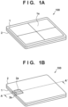
- FIGs. 1A and 1B are views showing the main arrangement of an imaging apparatus 100 which is a general radiation imaging apparatus (to be referred to as an imaging apparatus hereinafter).
- Fig. 1A shows a view seen from the side of the front surface of the imaging apparatus 100
- Fig. 1B shows a view seen from the side of the back surface of the imaging apparatus 100.
- the exterior of the imaging apparatus 100 is formed by a front housing 1 which includes a radiation reception surface 1a and a rear housing 2 which includes a radio transmission window 2a for allowing wireless communication.
- the exterior of the imaging apparatus 100 that is, the material of the front housing 1 and the rear housing 2 is a high-strength lightweight material such as CFRP, an aluminum alloy, a magnesium alloy, or the like.
- a material with good radiation transmittance needs to be selected for the radiation reception surface 1a of the front housing 1.
- the radiation reception surface 1a can be set as the opening, and a component that has high radiation transmittance and high rigidity such as CFRP or the like can be formed on the radiation reception surface 1a.
- Fig. 2 shows a sectional view taken along a line A - A' in Fig. 1B .
- a fluorescent material 3 that receives the radiation transmitted through an object and converts the received radiation into light is stacked on a sensor 4 which serves as a radiation detection unit.
- the converted light is converted into an electrical signal by the sensor 4.
- the sensor 4 is attached to a sensor holding member 6 via a radiation shielding material 5.
- GOS GadzOzS
- Csl is used as the material of the fluorescent material 3 to be stacked on the sensor 4.
- the sensor 4 since the sensor 4 is made of glass, the sensor will break if it receives a strong impact, load or displacement.
- an impact absorbing member 7 for absorbing an impact is arranged on the side of the radiation reception surface of the sensor 4.
- the radiation shielding material 5 has a function of protecting the electrical circuit boards from the radiation transmitted through the object and the sensor 4 and a function of preventing the radiation transmitted through the imaging apparatus 100 and scattered by a wall or the like behind the imaging apparatus from bouncing back and re-entering the fluorescent material 3 and the sensor 4.
- Mo, W, Pb, Al, Cu, SUS, barium sulfate, or the like tends to be employed as the material of the radiation shielding material.
- Electrical circuit boards 8a and 8b for reading out the electrical signals converted by the sensor 4 via a cable 9, an electrical circuit board 8c for generating a radiation image (image data) after the readout, and a communication module board 8d are installed on a surface facing a sensor attachment surface of the sensor holding member 6.
- the generated radiation image is transmitted to an external device (not shown) such as a PC, a tablet, or the like, and can be displayed to an operator or the like.
- the communication method may be wired communication or wireless communication, assume that the imaging apparatus 100 performs at least a wireless communication operation and includes a wireless communication unit 10.
- the wireless communication unit 10 performs communication on, for example, the 2.4 GHz band or the 5 GHz band.
- the radio transmission window 2a is arranged since the wireless radio waves will be shielded in a case in which the exterior of the imaging apparatus is made of a metallic material, and the wireless communication unit 10 is arranged at a position close to the radio transmission window 2a in consideration of the wireless radiation characteristics.
- Fig. 3 is a view of the arrangement of the imaging apparatus 100 in a case in which the rear housing 2 has been removed. Since the imaging apparatus 100 operates wirelessly, a power supply 11 for driving the imaging apparatus 100 has been included. In general, a secondary battery such as a lithium-ion battery, a lithium-ion capacitor, or the like tends to be employed as the power supply 11 to allow charging, but the arrangement is not limited to this. Also, although the power supply 11 is arranged to be incorporated in the imaging apparatus 100 in Fig. 3 , it may also be arranged to have a structure that considers the ease of detachability, and the power supply is not limited to an incorporated arrangement. A structure in which the power supply 11 is easily detachable may be, for example, a structure in which the power supply 11 can be directedly accessed without requiring the removal of the rear housing 2.
- FIG. 4 shows a sectional view of an imaging apparatus 200 according to this embodiment.
- Both of a front housing 1 and a rear housing 2, which are the exterior of the imaging apparatus 200, are formed by a non-metallic material (non-conductive member). Since a non-metallic material is used for the exterior, the electromagnetic shielding capability of the exterior will be very low, and the exterior will not become an obstacle for performing wireless communication. However, using a material with low electromagnetic shielding capability can greatly increase the possibility of artifact generation due to the application of electromagnetic waves to a sensor 4, electrical circuit boards 8a to 8c, a communication module board 8d, and a cable 9.
- the imaging apparatus 200 has a structure in which the above-described artifact generation is suppressed by covering the components inside the imaging apparatus 200 by a conductor 12.
- the conductor 12 suffices to be a conductor, and the material and the shape of the conductor 12 are not limited as long as a conductive film material, a sheet metal material, or the like is employed.
- the wireless radio waves will be shielded if a wireless communication unit 10 is covered by the conductor 12.
- the wireless communication unit 10 can be arranged between the conductor 12 and the exterior of the imaging apparatus 200 to allow radiation imaging to be performed without an obstacle to the wireless communication while taking a measure against electromagnetic noise.
- the material of the exterior is a non-metallic material, the entire exterior can become a wireless radio transmission window, thus increasing stability in the communication with an external communication unit.
- the conductor 12 since the wireless communication unit 10 and the communication module board 8d are connected by the cable 9, the conductor 12 has an opening 12a only for the cable 9 to pass through. Since the opening 12a is used for the purpose of passing the cable 9, it is preferable, from the point of view of electromagnetic shielding, for the opening 12a to have the smallest opening size as possible for the cable 9 to pass through. Note that although the wireless communication unit 10 is arranged on the back-surface side (the inner surface of the wall facing a radiation reception surface 1a) of the imaging apparatus 100 in Fig.
- the impact absorbing member 7 is arranged on the outside of the conductor 12 in a manner similar to the wireless communication unit 10, the impact absorbing member may also be covered by the conductor 12 in a manner similar to the sensor 4 and the like.
- the components inside the imaging apparatus 200 are covered by the conductor 12 to reduce the influence of electromagnetic waves from the wireless communication unit 10 on the internal components. As a result, the possibility that an artifact will be generated on a radiation image obtained by radiation imaging will be reduced.
- FIG. 5 is a sectional view of an imaging apparatus 300 according to this embodiment.
- conductors 12 are formed along an inner wall (inner surface) of a front housing 1 and an inner wall (inner surface) of a rear housing 2, respectively.
- Each conductor 12 may be a conductive film material or a sheet metal material in similar manner to the first embodiment or may be a conductive coating (conductive coating film) or a conductive plating.
- a conductive coating or plating is to be employed as the conductor 12
- communication with an external device can be performed without a problem by, for example, masking only the portion where a wireless communication unit 10 is to be arranged and arranging the wireless communication unit 10 at a location where an opening 12a has been formed.
- the conductor 12 is to be made of a conductive film material, a sheet metal material, or the like, it will be possible to perform communication with an external device without a problem in a similar manner to the above-described arrangement by forming the opening 12a in only a portion where the wireless communication unit 10 is to be arranged.
- Fig. 6 shows an imaging apparatus 400 as a modification of this embodiment.
- a conductive member 13 is formed so as to surround the wireless communication unit 10 to prevent the electromagnetic waves from the wireless communication unit 10 from entering inside the imaging apparatus 400.
- the conductive member 13 is electrically connected to the conductor 12.
- an opening 13a can be arranged in the conductive member 13 to allow the wireless communication unit 10 to be connected to a communication module board 8d.
- the opening 13a since the opening 13a is an opening for a cable 9 to pass through, it is preferable for the opening 13a to have the smallest opening size for the cable 9 to pass through.
- the conductors 12 are formed along the inner wall of the front housing 1 and the inner wall of the rear housing 2, respectively.
- the electromagnetic waves can be more effectively prevented from entering a sensor 4, electrical circuit boards 8a to 8c, and the like by forming the conductors 12 so as to be electrically connected in series.
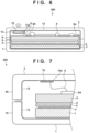
- Fig. 7 shows an enlarged view of a portion joining the front housing and the rear housing in a case in which the conductors 12 have been formed so as to be electrically connected in series in the imaging apparatus 300 ( Fig. 5 ).
- Fig. 7 shows an enlarged view of a portion joining the front housing and the rear housing in a case in which the conductors 12 have been formed so as to be electrically connected in series in the imaging apparatus 300 ( Fig. 5 ).
- the conductors 12, arranged on the side of the front housing 1 and the side of the rear housing 2, respectively, can be formed extending to the joint portions of the respective housings so that the conductors will overlap when the housings are joined. As a result, the conductors 12 will come into contact and become electrically connected when the imaging apparatus 300 is assembled. Also, in a case in which the conductors 12 are to be formed by the respective housings, it is preferable to form the conductors up to the positions that will not reach a side surface 1b of the front housing and a side surface 2b of the rear housing (that is, the outer walls), respectively, as shown in Fig. 7 in consideration of the entry of static electricity or the like from the outside.
- the components in the imaging apparatus 300 are covered by the conductors 12 formed along the inner sides of the respective housings. Furthermore, in the imaging apparatus 400 according to the modification, the wireless communication unit 10 is covered by the conductive member 13. Hence, the influence of electromagnetic waves from the wireless communication unit 10 on the internal components can be reduced. As a result, the possibility that an artifact will be generated on a radiation image obtained by radiation imaging will be reduced.
- FIG. 8 shows a sectional view of an imaging apparatus 500 according to this embodiment.
- a plurality of wireless communication units 10 have been arranged in the imaging apparatus 500 in consideration of communication stability in wireless communication.
- a radiation imaging apparatus can be installed in various kinds of places such as behind or underneath a patient, inside a bed, and the like when an imaging operation is to be performed. To transfer a radiation image to an external device immediately after an imaging operation, it is important for the radiation imaging apparatus to have a structure in which the wireless radio waves can be transmitted in all directions without any obstacles. Hence, as shown in Fig.
- the plurality of wireless communication units 10 have been arranged on at least one set of adjacent surfaces in the imaging apparatus 500.
- the imaging apparatus has a structure similar to that shown in Fig. 4 according to the first embodiment in that a sensor 4 and the like are covered by a conductor 12 and each wireless communication unit 10 is installed between the conductor 12 and a rear housing 2.
- the arrangement of the plurality of the wireless communication units 10 is not limited to that shown in Fig. 8 , and it may be arranged so that the plurality of the wireless communication units 10 are arranged on the same plane.
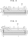
- Fig. 9 shows an imaging apparatus 600 according to a modification of this embodiment.
- the conductor 12 is formed along the inner walls (inner surfaces) of a front housing 1 and the rear housing 2.
- openings 12a for allowing communication by the respective wireless communication units 10 have been arranged
- a conductive member 13 has been installed in the periphery of the wireless communication unit 10 which is arranged on the side surface.
- a radiation shielding material 5 is made of a metallic material, a state in which the electromagnetic waves that enter from the opening 12a on the side of the back surface are absorbed by the radiation shielding material 5 before the electromagnetic waves reach the sensor 4 can be considered.
- the opening 12a on the side of the side surface is adjacent to the sensor 4, and there is nothing between the opening 12a on the side of the side surface and the sensor 4 to shield the electromagnetic waves.
- the conductive member 13 is arranged at the opening 12a of the side surface. In this case, it is preferable to arrange an opening 13a, which is to be provided in the conductive member 13, at a position far from the sensor 4, that is, a position closer to the side of the back surface than the radiation shielding material 5.
- the imaging apparatus 500 although the plurality of wireless communication units 10 are included to improve the communication stability, the influence of the electromagnetic waves from the wireless communication units 10 on the internal components is reduced by covering the internal components by the conductor 12. Furthermore, in the imaging apparatus 600 as a modification, the conductor 12 and the conductive member 13 are formed in accordance with the state of the periphery of the position of each of the plurality of wireless communication units 10 to effectively reduce the influence of the electromagnetic waves from the wireless communication units 10 on the internal components. As a result, the possibility that an artifact will be generated on a radiation image obtained by radiation imaging will be reduced.
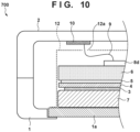
- FIG. 10 shows a sectional view of an imaging apparatus 700 according to this embodiment.
- the imaging apparatus 700 has a structure in which a front housing 1 is a separate component from a radiation reception surface 1a and the radiation reception surface 1a is a conductive member.
- a conductor 12 covers internal components other than a wireless communication unit 10 in the imaging apparatus 700, and each end of the conductor 12 is connected to the radiation reception surface 1a.
- the conductor 12 and the radiation reception surface 1a can be stably electrically connected by employing a method such as adhesion by a conductive adhesive or a conductive tape, fitting, or the like.
- a method such as adhesion by a conductive adhesive or a conductive tape, fitting, or the like.
- the conductor 12 and the radiation reception surface 1a can be electrically connected at the contact point of the front housing 1 and the radiation reception surface 1a shown in Fig. 10 .
- the property of a conductor 12 according to the embodiments described above can be changed in accordance with the position at which the conductor 12 is to be formed.
- the material quality, the thickness, the thermal conductivity, the radiation transmittance, the volume resistivity of the conductor 12, and the like may be changed between the side of the radiation reception surface and the side on the back surface of the imaging apparatus.
- the thickness if the thickness is increased, the thermal conductivity and the radiation transmittance will improve, and the electromagnetic waves can be shielded easily.
- the heat dissipation from each electrical circuit board can be dispersed, and it will be possible to further prevent the backscattering of radiation.
- the property of the conductor 12 can be controlled easily when the imaging apparatus has a structure in which the conductor 12 is divided between the side of a front housing 1 and the side of a rear housing 2 in the manner of an imaging apparatus 300 shown in Fig. 7 .
- the wireless communication unit 10 may also function as a non-contact power supplying unit to a power supply 11.
- One of the plurality of wireless communication units 10 shown in Figs. 8 and 9 may function as a power supplying unit in consideration of such an arrangement.
- the wireless communication unit 10 that is to function as the power supplying unit may be arranged on a side surface (an inner surface of an adjacent side wall of the radiation reception surface).
- the imaging apparatus is to be installed behind or underneath a patient or inside a bed, and arranging the wireless communication unit 10 that is to function as the power supplying unit on the side surface will make it easier for a corresponding power transmission unit (not shown) to connect when the power supply capacity of the power supply 11 has decreased during an imaging operation.
- the arrangement of the wireless communication unit 10 that is to function as a power supplying unit is not limited to this arrangement.
Landscapes
- Health & Medical Sciences (AREA)
- Life Sciences & Earth Sciences (AREA)
- Engineering & Computer Science (AREA)
- Physics & Mathematics (AREA)
- High Energy & Nuclear Physics (AREA)
- Molecular Biology (AREA)
- Medical Informatics (AREA)
- General Physics & Mathematics (AREA)
- Spectroscopy & Molecular Physics (AREA)
- Biomedical Technology (AREA)
- Public Health (AREA)
- Radiology & Medical Imaging (AREA)
- Optics & Photonics (AREA)
- Heart & Thoracic Surgery (AREA)
- Nuclear Medicine, Radiotherapy & Molecular Imaging (AREA)
- Surgery (AREA)
- Animal Behavior & Ethology (AREA)
- General Health & Medical Sciences (AREA)
- Pathology (AREA)
- Veterinary Medicine (AREA)
- Biophysics (AREA)
- Computer Networks & Wireless Communication (AREA)
- Computer Vision & Pattern Recognition (AREA)
- Theoretical Computer Science (AREA)
- Mathematical Physics (AREA)
- Measurement Of Radiation (AREA)
- Apparatus For Radiation Diagnosis (AREA)
Applications Claiming Priority (2)
| Application Number | Priority Date | Filing Date | Title |
|---|---|---|---|
| JP2018052918A JP7054356B2 (ja) | 2018-03-20 | 2018-03-20 | 放射線撮影装置 |
| PCT/JP2019/002683 WO2019181202A1 (ja) | 2018-03-20 | 2019-01-28 | 放射線撮影装置 |
Publications (3)
| Publication Number | Publication Date |
|---|---|
| EP3722837A1 EP3722837A1 (en) | 2020-10-14 |
| EP3722837A4 EP3722837A4 (en) | 2021-08-11 |
| EP3722837B1 true EP3722837B1 (en) | 2023-12-13 |
Family
ID=67986546
Family Applications (1)
| Application Number | Title | Priority Date | Filing Date |
|---|---|---|---|
| EP19770489.3A Active EP3722837B1 (en) | 2018-03-20 | 2019-01-28 | Radiation imaging device |
Country Status (6)
| Country | Link |
|---|---|
| US (1) | US11320546B2 (ko) |
| EP (1) | EP3722837B1 (ko) |
| JP (1) | JP7054356B2 (ko) |
| KR (2) | KR20230003404A (ko) |
| CN (1) | CN111684312B (ko) |
| WO (1) | WO2019181202A1 (ko) |
Families Citing this family (2)
| Publication number | Priority date | Publication date | Assignee | Title |
|---|---|---|---|---|
| KR102492247B1 (ko) * | 2021-01-08 | 2023-01-27 | (주)피코팩 | 센서 모듈 제조방법 및 이로부터 제조된 센서 모듈을 포함하는 x선 디텍터 |
| JP7482100B2 (ja) | 2021-12-09 | 2024-05-13 | キヤノン株式会社 | 放射線検出装置 |
Family Cites Families (36)
| Publication number | Priority date | Publication date | Assignee | Title |
|---|---|---|---|---|
| JPH07280944A (ja) | 1994-04-06 | 1995-10-27 | Morita Mfg Co Ltd | X線画像センサ、そのホルダおよびその位置決め具 |
| JP2003121553A (ja) * | 2001-08-06 | 2003-04-23 | Canon Inc | 放射線撮像装置 |
| JP2003101811A (ja) * | 2001-09-20 | 2003-04-04 | Sony Corp | 通信システムおよびその方法と表示装置 |
| JP2004252562A (ja) | 2003-02-18 | 2004-09-09 | Konica Minolta Holdings Inc | データ処理装置 |
| US7495226B2 (en) * | 2006-05-26 | 2009-02-24 | Carestream Health, Inc. | Compact and durable encasement for a digital radiography detector |
| JP5170232B2 (ja) * | 2008-02-28 | 2013-03-27 | 日本電気株式会社 | 電磁シールド構造およびそれを用いた無線装置、電磁シールドの製造方法 |
| JP2010276687A (ja) | 2009-05-26 | 2010-12-09 | Fujifilm Corp | 放射線検出装置及び放射線画像撮影システム |
| JP5238652B2 (ja) | 2009-09-11 | 2013-07-17 | 富士フイルム株式会社 | 放射線画像撮影装置 |
| JP5451341B2 (ja) | 2009-11-27 | 2014-03-26 | キヤノン株式会社 | 放射線画像撮影装置 |
| WO2011142157A1 (ja) | 2010-05-12 | 2011-11-17 | コニカミノルタエムジー株式会社 | 放射線画像撮影システム |
| JP2011247684A (ja) * | 2010-05-25 | 2011-12-08 | Fujifilm Corp | 放射線画像撮影装置及びその組立方法 |
| CN103109526B (zh) | 2010-07-16 | 2016-08-03 | 富士胶片株式会社 | 放射线图像捕捉设备、放射线图像捕捉系统、放射线图像捕捉方法、以及程序 |
| JP2012112699A (ja) | 2010-11-22 | 2012-06-14 | Fujifilm Corp | 放射線検出パネル及び放射線撮像装置 |
| JP5694892B2 (ja) * | 2011-10-19 | 2015-04-01 | 富士フイルム株式会社 | 放射線画像撮影装置 |
| US8891733B2 (en) * | 2012-05-11 | 2014-11-18 | General Electric Company | Power and communication interface between a digital X-ray detector and an X-ray imaging system |
| JP6227227B2 (ja) | 2012-05-31 | 2017-11-08 | コニカミノルタ株式会社 | 放射線画像撮影装置 |
| JP5815483B2 (ja) | 2012-07-27 | 2015-11-17 | 富士フイルム株式会社 | 放射線画像撮影装置 |
| JP2014178308A (ja) * | 2013-02-12 | 2014-09-25 | Fujifilm Corp | 電子カセッテ |
| JP6224901B2 (ja) | 2013-03-14 | 2017-11-01 | キヤノン株式会社 | 移動型放射線画像撮影装置、移動型放射線画像撮影装置の制御方法、プログラム |
| JP5627049B2 (ja) | 2013-06-07 | 2014-11-19 | 富士フイルム株式会社 | 電子カセッテ |
| JP2015025682A (ja) | 2013-07-24 | 2015-02-05 | キヤノン株式会社 | 放射線撮影装置 |
| JP6397208B2 (ja) | 2014-04-09 | 2018-09-26 | キヤノン株式会社 | 放射線画像撮影装置および放射線画像撮影システム |
| JP2015208573A (ja) | 2014-04-28 | 2015-11-24 | キヤノン株式会社 | 放射線発生用装置 |
| JP6433183B2 (ja) | 2014-07-23 | 2018-12-05 | キヤノン株式会社 | 放射線検出装置および放射線撮影システム |
| JP6259382B2 (ja) | 2014-09-22 | 2018-01-10 | 富士フイルム株式会社 | 電子カセッテ |
| JP6251147B2 (ja) * | 2014-09-29 | 2017-12-20 | 富士フイルム株式会社 | 電子カセッテおよび電子カセッテの作動方法 |
| JP6714332B2 (ja) * | 2014-12-22 | 2020-06-24 | キヤノン株式会社 | 放射線検出装置、及び放射線撮像システム |
| JP6558909B2 (ja) | 2015-02-09 | 2019-08-14 | キヤノン株式会社 | 放射線撮像装置、その制御方法およびプログラム |
| JP6650676B2 (ja) | 2015-02-26 | 2020-02-19 | キヤノン株式会社 | 放射線撮像装置および放射線撮像システム |
| JP6502731B2 (ja) | 2015-04-13 | 2019-04-17 | キヤノン株式会社 | 放射線撮像装置及び放射線撮像システム |
| JP6553929B2 (ja) * | 2015-04-13 | 2019-07-31 | キヤノン株式会社 | 放射線撮像装置および撮像システム |
| JP6633864B2 (ja) | 2015-08-07 | 2020-01-22 | キヤノン株式会社 | 放射線撮像装置及び放射線撮像システム |
| JP6606388B2 (ja) | 2015-09-29 | 2019-11-13 | キヤノン株式会社 | 放射線撮影装置および放射線撮影システム |
| JP2018004520A (ja) | 2016-07-06 | 2018-01-11 | コニカミノルタ株式会社 | 放射線画像撮影装置 |
| JP7007555B2 (ja) | 2016-09-27 | 2022-02-10 | セントラル硝子株式会社 | 不飽和結合含有シラン化合物の精製方法及び製造方法 |
| JP2017070766A (ja) * | 2016-11-22 | 2017-04-13 | 株式会社根本杏林堂 | 磁気共鳴撮像システム |
-
2018
- 2018-03-20 JP JP2018052918A patent/JP7054356B2/ja active Active
-
2019
- 2019-01-28 EP EP19770489.3A patent/EP3722837B1/en active Active
- 2019-01-28 KR KR1020227044482A patent/KR20230003404A/ko not_active Application Discontinuation
- 2019-01-28 CN CN201980011446.5A patent/CN111684312B/zh active Active
- 2019-01-28 KR KR1020207029124A patent/KR102560275B1/ko active IP Right Grant
- 2019-01-28 WO PCT/JP2019/002683 patent/WO2019181202A1/ja unknown
-
2020
- 2020-07-15 US US16/929,815 patent/US11320546B2/en active Active
Also Published As
| Publication number | Publication date |
|---|---|
| KR102560275B1 (ko) | 2023-07-28 |
| US20200348427A1 (en) | 2020-11-05 |
| KR20230003404A (ko) | 2023-01-05 |
| CN111684312A (zh) | 2020-09-18 |
| EP3722837A4 (en) | 2021-08-11 |
| KR20200130853A (ko) | 2020-11-20 |
| CN111684312B (zh) | 2024-03-19 |
| EP3722837A1 (en) | 2020-10-14 |
| US11320546B2 (en) | 2022-05-03 |
| JP7054356B2 (ja) | 2022-04-13 |
| WO2019181202A1 (ja) | 2019-09-26 |
| JP2019164069A (ja) | 2019-09-26 |
Similar Documents
| Publication | Publication Date | Title |
|---|---|---|
| CN102630309B (zh) | 放射线摄像设备 | |
| JP5743477B2 (ja) | 放射線撮影用装置 | |
| JP4408128B2 (ja) | 携帯端末装置 | |
| EP3722837B1 (en) | Radiation imaging device | |
| JP6486314B2 (ja) | 車載用アンテナ装置 | |
| JP5627049B2 (ja) | 電子カセッテ | |
| US10955571B2 (en) | Radiographing apparatus and radiographing system | |
| JP2015197663A (ja) | 放射線撮影装置および放射線撮影システム | |
| KR101927690B1 (ko) | 방사선 촬상 시스템 | |
| JP7467711B2 (ja) | 放射線撮影装置 | |
| CN112083380A (zh) | 一种电磁兼容的红外/雷达复合导引头 | |
| JP7043305B2 (ja) | 放射線撮影装置および放射線撮影システム | |
| JP7446762B2 (ja) | 放射線撮影装置 | |
| JP2018004520A (ja) | 放射線画像撮影装置 | |
| US20230184965A1 (en) | Radiation detection apparatus | |
| JP7427441B2 (ja) | 放射線撮影装置 | |
| US20220317320A1 (en) | X-ray detectors with plastic housings | |
| JP5709972B2 (ja) | 放射線画像撮影装置 | |
| JP2022111805A (ja) | 放射線撮影装置 | |
| JP2021105539A (ja) | 放射線撮影装置 | |
| CN115590539A (zh) | 放射线摄像装置 | |
| JP2021060340A (ja) | 放射線撮影装置 |
Legal Events
| Date | Code | Title | Description |
|---|---|---|---|
| STAA | Information on the status of an ep patent application or granted ep patent |
Free format text: STATUS: THE INTERNATIONAL PUBLICATION HAS BEEN MADE |
|
| PUAI | Public reference made under article 153(3) epc to a published international application that has entered the european phase |
Free format text: ORIGINAL CODE: 0009012 |
|
| STAA | Information on the status of an ep patent application or granted ep patent |
Free format text: STATUS: REQUEST FOR EXAMINATION WAS MADE |
|
| 17P | Request for examination filed |
Effective date: 20200708 |
|
| AK | Designated contracting states |
Kind code of ref document: A1 Designated state(s): AL AT BE BG CH CY CZ DE DK EE ES FI FR GB GR HR HU IE IS IT LI LT LU LV MC MK MT NL NO PL PT RO RS SE SI SK SM TR |
|
| AX | Request for extension of the european patent |
Extension state: BA ME |
|
| DAV | Request for validation of the european patent (deleted) | ||
| DAX | Request for extension of the european patent (deleted) | ||
| A4 | Supplementary search report drawn up and despatched |
Effective date: 20210709 |
|
| RIC1 | Information provided on ipc code assigned before grant |
Ipc: G01T 7/00 20060101AFI20210705BHEP Ipc: A61B 6/00 20060101ALI20210705BHEP Ipc: G01T 1/20 20060101ALI20210705BHEP |
|
| RAP3 | Party data changed (applicant data changed or rights of an application transferred) |
Owner name: CANON KABUSHIKI KAISHA |
|
| STAA | Information on the status of an ep patent application or granted ep patent |
Free format text: STATUS: EXAMINATION IS IN PROGRESS |
|
| 17Q | First examination report despatched |
Effective date: 20221122 |
|
| GRAP | Despatch of communication of intention to grant a patent |
Free format text: ORIGINAL CODE: EPIDOSNIGR1 |
|
| STAA | Information on the status of an ep patent application or granted ep patent |
Free format text: STATUS: GRANT OF PATENT IS INTENDED |
|
| INTG | Intention to grant announced |
Effective date: 20230711 |
|
| GRAS | Grant fee paid |
Free format text: ORIGINAL CODE: EPIDOSNIGR3 |
|
| GRAA | (expected) grant |
Free format text: ORIGINAL CODE: 0009210 |
|
| STAA | Information on the status of an ep patent application or granted ep patent |
Free format text: STATUS: THE PATENT HAS BEEN GRANTED |
|
| AK | Designated contracting states |
Kind code of ref document: B1 Designated state(s): AL AT BE BG CH CY CZ DE DK EE ES FI FR GB GR HR HU IE IS IT LI LT LU LV MC MK MT NL NO PL PT RO RS SE SI SK SM TR |
|
| REG | Reference to a national code |
Ref country code: GB Ref legal event code: FG4D |
|
| REG | Reference to a national code |
Ref country code: CH Ref legal event code: EP |
|
| REG | Reference to a national code |
Ref country code: DE Ref legal event code: R096 Ref document number: 602019043279 Country of ref document: DE |
|
| REG | Reference to a national code |
Ref country code: IE Ref legal event code: FG4D |
|
| PG25 | Lapsed in a contracting state [announced via postgrant information from national office to epo] |
Ref country code: GR Free format text: LAPSE BECAUSE OF FAILURE TO SUBMIT A TRANSLATION OF THE DESCRIPTION OR TO PAY THE FEE WITHIN THE PRESCRIBED TIME-LIMIT Effective date: 20240314 |
|
| REG | Reference to a national code |
Ref country code: LT Ref legal event code: MG9D |
|
| PG25 | Lapsed in a contracting state [announced via postgrant information from national office to epo] |
Ref country code: LT Free format text: LAPSE BECAUSE OF FAILURE TO SUBMIT A TRANSLATION OF THE DESCRIPTION OR TO PAY THE FEE WITHIN THE PRESCRIBED TIME-LIMIT Effective date: 20231213 |
|
| REG | Reference to a national code |
Ref country code: NL Ref legal event code: MP Effective date: 20231213 |
|
| PG25 | Lapsed in a contracting state [announced via postgrant information from national office to epo] |
Ref country code: ES Free format text: LAPSE BECAUSE OF FAILURE TO SUBMIT A TRANSLATION OF THE DESCRIPTION OR TO PAY THE FEE WITHIN THE PRESCRIBED TIME-LIMIT Effective date: 20231213 |
|
| PG25 | Lapsed in a contracting state [announced via postgrant information from national office to epo] |
Ref country code: LT Free format text: LAPSE BECAUSE OF FAILURE TO SUBMIT A TRANSLATION OF THE DESCRIPTION OR TO PAY THE FEE WITHIN THE PRESCRIBED TIME-LIMIT Effective date: 20231213 Ref country code: GR Free format text: LAPSE BECAUSE OF FAILURE TO SUBMIT A TRANSLATION OF THE DESCRIPTION OR TO PAY THE FEE WITHIN THE PRESCRIBED TIME-LIMIT Effective date: 20240314 Ref country code: ES Free format text: LAPSE BECAUSE OF FAILURE TO SUBMIT A TRANSLATION OF THE DESCRIPTION OR TO PAY THE FEE WITHIN THE PRESCRIBED TIME-LIMIT Effective date: 20231213 Ref country code: BG Free format text: LAPSE BECAUSE OF FAILURE TO SUBMIT A TRANSLATION OF THE DESCRIPTION OR TO PAY THE FEE WITHIN THE PRESCRIBED TIME-LIMIT Effective date: 20240313 |
|
| PGFP | Annual fee paid to national office [announced via postgrant information from national office to epo] |
Ref country code: DE Payment date: 20231219 Year of fee payment: 6 |
|
| REG | Reference to a national code |
Ref country code: AT Ref legal event code: MK05 Ref document number: 1640905 Country of ref document: AT Kind code of ref document: T Effective date: 20231213 |
|
| PG25 | Lapsed in a contracting state [announced via postgrant information from national office to epo] |
Ref country code: NL Free format text: LAPSE BECAUSE OF FAILURE TO SUBMIT A TRANSLATION OF THE DESCRIPTION OR TO PAY THE FEE WITHIN THE PRESCRIBED TIME-LIMIT Effective date: 20231213 |