EP3682461B1 - Thermally assisted negative electron affinity photocathode - Google Patents
Thermally assisted negative electron affinity photocathode Download PDFInfo
- Publication number
- EP3682461B1 EP3682461B1 EP18856829.9A EP18856829A EP3682461B1 EP 3682461 B1 EP3682461 B1 EP 3682461B1 EP 18856829 A EP18856829 A EP 18856829A EP 3682461 B1 EP3682461 B1 EP 3682461B1
- Authority
- EP
- European Patent Office
- Prior art keywords
- layer
- photocathode
- barrier
- barrier layer
- optical absorber
- Prior art date
- Legal status (The legal status is an assumption and is not a legal conclusion. Google has not performed a legal analysis and makes no representation as to the accuracy of the status listed.)
- Active
Links
Images


Classifications
-
- H—ELECTRICITY
- H01—ELECTRIC ELEMENTS
- H01J—ELECTRIC DISCHARGE TUBES OR DISCHARGE LAMPS
- H01J1/00—Details of electrodes, of magnetic control means, of screens, or of the mounting or spacing thereof, common to two or more basic types of discharge tubes or lamps
- H01J1/02—Main electrodes
- H01J1/34—Photo-emissive cathodes
-
- H—ELECTRICITY
- H01—ELECTRIC ELEMENTS
- H01J—ELECTRIC DISCHARGE TUBES OR DISCHARGE LAMPS
- H01J31/00—Cathode ray tubes; Electron beam tubes
- H01J31/08—Cathode ray tubes; Electron beam tubes having a screen on or from which an image or pattern is formed, picked up, converted, or stored
- H01J31/26—Image pick-up tubes having an input of visible light and electric output
- H01J31/48—Tubes with amplification of output effected by electron multiplier arrangements within the vacuum space
-
- H—ELECTRICITY
- H01—ELECTRIC ELEMENTS
- H01J—ELECTRIC DISCHARGE TUBES OR DISCHARGE LAMPS
- H01J2201/00—Electrodes common to discharge tubes
- H01J2201/34—Photoemissive electrodes
- H01J2201/342—Cathodes
- H01J2201/3421—Composition of the emitting surface
- H01J2201/3423—Semiconductors, e.g. GaAs, NEA emitters
-
- H—ELECTRICITY
- H01—ELECTRIC ELEMENTS
- H01J—ELECTRIC DISCHARGE TUBES OR DISCHARGE LAMPS
- H01J2231/00—Cathode ray tubes or electron beam tubes
- H01J2231/50—Imaging and conversion tubes
- H01J2231/501—Imaging and conversion tubes including multiplication stage
-
- H—ELECTRICITY
- H01—ELECTRIC ELEMENTS
- H01J—ELECTRIC DISCHARGE TUBES OR DISCHARGE LAMPS
- H01J29/00—Details of cathode-ray tubes or of electron-beam tubes of the types covered by group H01J31/00
- H01J29/02—Electrodes; Screens; Mounting, supporting, spacing or insulating thereof
- H01J29/04—Cathodes
-
- H—ELECTRICITY
- H01—ELECTRIC ELEMENTS
- H01J—ELECTRIC DISCHARGE TUBES OR DISCHARGE LAMPS
- H01J31/00—Cathode ray tubes; Electron beam tubes
- H01J31/08—Cathode ray tubes; Electron beam tubes having a screen on or from which an image or pattern is formed, picked up, converted, or stored
- H01J31/49—Pick-up adapted for an input of electromagnetic radiation other than visible light and having an electric output, e.g. for an input of X-rays, for an input of infrared radiation
Definitions
- This invention falls in the field of effectively negative electron affinity semiconductor photocathodes.
- This invention describes a new photocathode structure incorporating a single small conduction band barrier between an optical absorber layer and an effectively negative electron affinity photocathode emission surface.
- This thermally assisted negative electron affinity (TANEA) photocathode is appropriate for use in photomultiplier tubes and night vision sensors.
- This invention will have the greatest benefit for photocathodes in the visible and near infrared portion of the spectrum, designed to operate above cryogenic temperatures.
- Photocathodes come in a wide variety of types and subclasses. Many of the early night image intensifiers employed Multialkali Antimonide Photocathodes as described by Sommer in Photoemissive Materials, A. H. Sommer, Robert E. Krieger Publishing Company, Huntington, New York, 1980 . Modern versions of these photocathodes account for a significant fraction of the image intensifiers sold and in use today. In the 1950s, research on a new class of photocathodes was anchored and accelerated when William E. Spicer reported a detailed photocathode model in Phys. Rev. 112, 114 (1958 ) to give understanding of photocathode device physics and permit engineering of photocathodes for specific performance characteristics.
- U.S. Patent 3,631,303 details one of the early NEA photocathode designs that employs a band-gap graded semiconductor optical absorber layer.
- the semiconductor substrate is a large band-gap material that acts as a passivation layer for the back surface of the active layer.
- the structure works equally well in a transmission mode.
- a modern third generation image intensifier photocathode as disclosed in U.S. Patent 5,268,570 makes use of a p-type GaAs or InGaAs optical absorber layer coupled with a p-type AlGaAs window layer.
- An example and method of manufacture of a modern GaAs photocathode is described in U.S. Patent 5,597,112 .
- Photoelectrons that diffuse to the hetero-junction experience a potential barrier and are reflected back into the absorber layer and hence, toward the vacuum emission surface.
- the ramped band-gap structure described in 3,631,303 plays a similar role in directing the diffusion / drift of photoelectrons toward the vacuum emission surface.
- US Patent 5,712,490 describes a photocathode incorporating a combined compositional ramp and a predetermined doping profile near the emission surface of the photocathode "for maintaining the conduction band of the device flat until the emission surface" in order to increase photoresponse.
- purpose-specific photocathodes incorporating sophisticated quantum well structures have been designed for use in electron accelerators; US Patent 8,143,615 describes such a structure.
- the superlattice structure cited in US Patent 8,143,615 incorporates a series of barriers and wells designed to produce a mini-band allowing high brightness monochromatized electron emission. Fundamental to the design of the photocathode, photogenerated electrons transit the barriers between the individual quantum wells via tunneling thereby creating the mini-bands.
- Document US 2002/180343 describes a cathode structure for an image intensifier tube being operated to extend the spectral range of an image intensifier to the short wavelength infrared (SWIR) range of the electromagnetic spectrum.
- a cathode structure is a heterojunction of GaSb and GaAs, the GaSb material is to absorb the radiation and the GaAs is for emission characteristics.
- the semiconductor NEA photocathodes sited in the previous paragraphs can be classed as passive photocathodes.
- these cathodes are set to a single fixed electrical potential. In other words, there are no electric fields within the cathode that are specified through the application of an electrical bias voltage across two or more contact terminals.
- Embodiments of the current invention fall into the class of passive photocathodes.
- the invention is set forth in the claims.
- a passive p-type semiconductor photocathode includes a barrier or rise in the conduction band energy as referenced to the Fermi level falling between an optical absorber layer and the vacuum emission surface of the photocathode.
- a barrier in the conduction band may appear to be counterintuitive, it allows a trade-off to be made between photoelectron transport efficiency to the emission surface and photoelectron escape probability.
- photoelectron transport efficiency to the emission surface decreases as the conduction band barrier height is increased.
- NEA photocathode escape probability generally increases with increasing energy spread between the conduction band at the surface and the Fermi level.
- photo-generated electron escape probability generally increases as the barrier height increases for those electrons that successfully transit over the barrier.
- This disclosure teaches that the rate of increase in escape probability can exceed the loss of photoelectron transport efficiency as the barrier height is increased for a range of photocathodes, including the economically important GaAs photocathode, when operated near room temperature or at temperatures greater than -40 degrees C as is relevant for use of night vision devices in Arctic environments.
- the barrier thickness is set to be sufficient to ensure that transmission of photoelectrons across the barrier is dominated by thermally excited electrons with sufficient energy to exceed the barrier height at the designated operating temperature as opposed to tunneling through the barrier. Additionally, the combined thickness and doping level of the barrier is sufficient to ensure that any depletion layer that may form beneath the semiconductor surface does not penetrate the barrier layer to the point where the barrier layer is fully depleted or reduce the effective barrier thickness to the point where tunneling through the energy barrier predominates.
- a barrier meeting the previously stated requirements may be referred to as a thermionic emission barrier.
- Thermalized photoelectrons in the conduction band have a finite chance of transiting the barrier layer of the photocathode due to thermionic excitation over the conduction band barrier.
- Photoelectrons which transit over the conduction band barrier benefit from an increase in escape probability from a proximate negative electron affinity vacuum interface when compared to a photocathode structure lacking the barrier. This demonstrated improved level of performance may be qualitatively explained via two key observations:
- TNEA thermally assisted negative electron affinity
- Figure 1A illustrates a schematic of a thermally assisted negative electron affinity (NEA) according to one embodiment.
- the device comprises an optical window layer 105, an optical absorber layer 110, and a thermionic emission layer 115.
- Table 1 further describes the active semiconductor layers of an embodiment of the thermally assisted negative electron affinity photocathode depicted schematically in Figure 1A . The layers are listed in the order they are encountered by incoming light in a transmission mode structure.
- a method to attach a semiconductor photocathode to a glass window is detailed in US Patent 3,769,536 .
- Corning Code 7056 or a glass of similar expansion can be used via glass bonding as a support structure for GaAs photocathodes such as the one described in Figure 1A and Table 1.
- photoresponse may be further improved through the use of anti-reflection coatings (ARCs).
- ARCs may be beneficially added both onto the exposed glass surface and between the glass to semiconductor interface.
- a SiN x O y layer with an appropriate index of refraction and thickness can be used as an antireflection coating at the semiconductor - glass interface.
- a variety of coatings such as MgF may be used on the exposed glass surface.
- the photocathode must be brought into an effective negative electron affinity (NEA) state.
- NAA negative electron affinity
- the conventional nomenclature is used of referring to a cathode as being in an effective state of negative electron affinity if the undepleted portion of the conduction band of the barrier layer lies above the energy of a free electron in vacuum.
- a photocathode may be chemically cleaned, then given a vacuum thermal cycle in order to desorb any residual surface contaminants and finally coated with work function reducing materials such as, but not limited to, Rb+O 2 , Cs+O 2 or Cs+NF 3 .
- Csorba provides details on all of the major photocathode manufacturing steps from cathode growth through the deposition of a work-function lowering Cs+O 2 coating; to the extent that new materials are added in layer 115, one skilled in the art may fine tune the described processes, if required, in order to achieve the desired results.
- GaAs photocathode activation physics is described in detail by: Applied Physics A: Materials Science & Processing (Historical Archive)
- Negative affinity 3-5 photocathodes Their physics and technology by W. E. Spicer, Issue: Volume 12, Number 2, Date: February 1977 Pages: 115 - 130 .
- FIG. 1A shows a schematic depiction of the active semiconductor layers which constitute a basic embodiment of the thermally assisted negative electron affinity (TANEA) photocathode.
- TNEA thermally assisted negative electron affinity
- Light may enter either side of the photocathode.
- the structure is often employed as a transmission mode photocathode. In the case of transmission mode operation, light will enter the photocathode through layer 105.
- Layer 105 is a p-doped semiconductor layer where the bandgap of the semiconductor is larger than that of the p-doped semiconductor layer designated 110.
- the doping and thickness of layer 105 are chosen such that several criteria are met.
- the thickness and the doping of layer 105 are chosen such that any transferred charge or interface states present on the surfaces of layer 105 are compensated by the p-type dopant without fully depleting the layer.
- the dopant level and thickness of layer 105 is chosen such that the un-depleted thickness of the layer is sufficient to prevent meaningful tunneling of charge to or from the conduction band of semiconductor layer 110.
- Table 1 an Al 0.8 Ga 0.2 As layer p-doped to 6E18cm -3 at a thickness of 0.1microns, meets these criteria.
- Layer 105 is often referred to as a window layer in that for a transmission mode application of the photocathode, light that has an energy falling below the bandgap energy of layer 105 may enter the photocathode with minimal absorption similar to light passing through an optical window.
- a semiconductor heterojunction is formed at the interface of layers 105 and 110. Materials 105 and 110 are chosen such that the heterojunction provides a low interface recombination velocity for electrons residing in the conduction band of layer 110.
- Layer 110 is a p-type semiconductor layer. The absorption coefficient and thickness of layer 110 typically determine the spectral response of the photocathode. Incident light transmitted through layer 105 is absorbed in layer 110. Layer 110 is often referred to as an absorber layer.
- photoelectrons generated via the absorption of light in layer 110 are subsequently transported to the interface between layer 110 and 115.
- the thickness and doping of layer 110 are typically chosen as a compromise between a number of factors. Those factors include the absorption coefficient for the wavelength range of interest, the temperature range of interest, the photoelectron (minority carrier) diffusion length and the energy difference between the Fermi level and the conduction band.
- the values quoted in Table 1 for layer 110 are reasonable choices for a room temperature photocathode designed to image at night under natural starlight conditions.
- Layer 115 is designed so as to result in a conduction band barrier when compared to layer 110.
- This barrier may be introduced via an increase in the bandgap of layer 115 relative to layer 110 forming a heterojunction or by an increase in the p-type doping concentration of layer 115 relative to layer 110 or by a combination of these two methods.
- the heterojunction may be formed by a distinct atomically sharp transition or via a short ramp in the atomic constituents of the layer. Any ramp, if present, should be much shorter than the characteristic minority carrier diffusion length of the photoelectrons.
- Layer 115 may be referred to as a barrier layer due to the fact that the increase in the conduction band energy relative to layer 110 will generally decrease the efficiency of photoelectron transport toward the photoemission surface. In this embodiment, layer 115 also plays the role of the photoemission surface.
- Al X Ga (1-X) As a subset of the material family Al X Ga (1-X) As Y P (1-Y) has been shown to be easily controllable and therefore is favored as a practical embodiment for layer 115.
- Al X Ga (1-X) As compositions where X is less than -0.1% show little practical benefit over GaAs.
- Al X Ga (1-X) As compositions with X values greater than -0.04 resulted in excessive photoelectron transport losses. Consequently, initial prototype photocathodes targeted X values ranging from -0.001 to 0.04.
- the photocathode may be bonded to a support window.
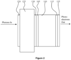
- Figure 2 schematically depicts the photocathode described in Table 1 after it has been anti-reflection coated and bonded to a transparent support substrate or window
- the assembly is depicted as a transmission mode photocathode.
- the decision to employ this embodiment in a transmission mode photocathode is not meant as a limit on this disclosure, but rather just as one example.
- the disclosed structures will also yield performance benefits for reflection mode photocathodes.
- the first layer encountered by the light is an anti-reflection coating designated as 120.
- Layer 120 may be a simple MgF 1 ⁇ 4-wave coating at the wavelength of interest or it may be a multi-layer coating designed for a specific set of targeted wavelengths or wavelength band. Alternatively, this layer may be omitted without impacting the intent of this disclosure.
- the second layer encountered by the incoming light is the transparent support substrate depicted as layer 125.
- Layer 125 may be fabricated from Corning code 7056 glass or another transparent material. Corning code 7056 glass has been demonstrated to be a suitable support substrate for glass bonded GaAs based photocathodes.
- the next layer encountered by the incoming light is layer 130.
- Layer 130 is an anti-reflection coating designed to minimize light loss as the incoming light transitions from layer 125 and enters the photocathode structure.
- Layer 130 may be formed from SiO x N y a material composed of silicon oxygen and nitrogen at a composition and thickness designed to achieve a minimum total reflection loss over the desired operational wavelength band of the photocathode.
- the first layer of the photocathode is layer 105, the window layer.
- the window layer is designed to have a larger bandgap than the optical absorber layer 110, both to allow light to pass easily through the window layer and to specify a low loss electron recombination velocity interface with the optical absorber layer.
- the light in the wavelength band of interest is primarily absorbed in layer 110 the optical absorber layer. Absorption of the light in layer 110 results in the generation of electron hole pairs where the electrons thermalize to the conduction band minimum reside of layer 110. Diffusion transports the photoelectrons in the conduction band to the barrier layer (115) interface where the most energetic of the electrons in the thermalized electron energy distribution have a higher probability of diffusing across to the activation layer 135. As the energetic electrons approach the interface between layer 115 and 135, they will encounter an electric field that will tend to accelerate the electrons toward the vacuum lying beyond the surface of layer 135. A significant fraction of the energetic electrons entering the activation layer will subsequently be emitted from the surface of the photocathode assembly.
- Layer 135 may be composed of Cesium and Oxygen. Methods of forming an efficient activation layer are well known to those skilled in the art. The exact composition of the activation layer is not material to the teaching of this disclosure.
- FIG. 3 is a schematic bandgap diagram of Thermally Assisted Negative Electron Affinity Photocathode containing an additional layer to modify photocathode surface chemistry.
- Table 2 Layer Number Composition Doping #/cm 3 Thickness Microns Layer Title / Function 105 Al 0.8 Ga 0.2 As P-type, 6x10 18 0.1
- Optical window layer 110 GaAs P-type, 3x10 18 2
- Thermionic Emission Barrier 140 GaAs P-type, 7x10 18 .005 Surface Specification Layer
- the alternate embodiment depicted in Figure 3 interposed an additional emitter or emission layer between the thermionic barrier layer and the vacuum surface.
- the primary purpose of this layer is to specify a surface chemistry on the vacuum surface of the photocathode which is conducive to the formation of a stable, high efficiency activation layer.
- the photocathodes will exhibit a relatively high work function.
- the semiconductor surface In order to produce a surface that exhibits a high photoelectron escape probability, the semiconductor surface must first be cleaned to remove surface contaminants including native oxides. Numerous methods have been detailed in the literature to achieve an atomically clean surface including wet cleaning with HCl solutions to remove bulk surface oxides, heat cleaning to desorb residual oxides, adsorbed contaminants and atomic hydrogen cleaning.
- Aluminum oxide is a particularly difficult oxide to remove.
- the presence of aluminum oxide may interfere with the ability to form a high efficiency photocathode.
- a thin GaAs layer 140 may be formed over the barrier layer in order to eliminate the presence of native aluminum oxide on the surface of the photocathode.
- the use of thin GaAs surface layers does not negate the benefit of the thermionic emission barrier layer. Both doped as shown in Table 2 and intrinsic (nonintentionally doped) GaAs surface layers have been tested at thicknesses up to 10nm with good results.
- the GaAs surface layer may be beneficial to incorporate in a thickness range between that of a single atomic layer up to a thickness of in excess of 30nm.
- a work-function lowering coating such as Cs-O.
- any of the III-V semiconductor family of compounds may be used to design applicable TANEA photocathodes
- Group 5 elements that are specifically envisioned as being applicable include Aluminum, Gallium and Indium.
- Group 3 elements envisioned as suitable photocathode constituents include Nitrogen, Phosphorus, Arsenic and Antimony.
- FIG. 4B The data is replotted in Figure 4B where the barrier height is now normalized as a fraction of kT where k is the Boltzmann Constant and T is the Kelvin temperature at which the measurements were made (-295K). Although no new information is incorporated in Figure 4B , it illustrates how a photocathode engineer may approach optimizing a TANEA photocathode for operation over a specific temperature range. The response versus barrier height curve will be different for each material system based on a wide range of material quality and interface properties.
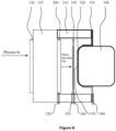
- FIG 5 is a schematic depiction of a vacuum image sensor incorporating a TANEA photocathode and an electron sensitive imager, such as an electron sensitive CMOS image sensor or an electron sensitive CCD.
- Layer 120 on the optical input surface is an antireflection coating as previously described in regards to Figure 2 .
- 125 represents a transparent window (or substrate) as described in the Figure 2 detailed description. In this case, the transparent window is used to form a portion of the vacuum envelope required to preserve a high level of sensitivity from the TANEA photocathode.
- the activation layer of the photocathode is particularly sensitive to contamination from oxygen, water and a wide variety of other trace gasses.
- the volume depicted by 200 represents the sum of the layers previously described in Figure 2 as the balance of the TANEA photocathode assembly. Specifically, layers 130, 105, 110, 115 and 135 respectively as described in Figure 2 are included and schematically represented as 200. This description is not meant to restrict the choice of the photocathode engineer, an equally acceptable embodiment may include layers 140 as described in Figure 3 between previously described layers 115 and 135. Reference 210 represents that portion of the vacuum sensor body that makes up the side-walls of the sensor.
- Vacuum seals are formed on opposing surfaces of 210 in order to maintain a continuous unbroken vacuum envelope around the vacuum emission surface of the TANEA photocathode and the subsequent path of the emitted photoelectrons.
- 210 may be composed of a ceramic material such as Al 2 O 3 .
- 250 schematically represents an electrical connection from the outside of the vacuum envelope to the TANEA photocathode. The path of 250 is inconsequential to the intent of this disclosure as long as vacuum integrity is not compromised. An Ohmic contact between 250 and the semiconductor material of the TANEA photocathode is preferred.
- Reference 230 represents the vacuum enclosure completing the vacuum envelope opposite to the photocathode. This surface may be fabricated from a multi-layer ceramic block incorporating multiple electrical feedthroughs 240. 230 additionally may be used to physically mount an electron imaging sensor 220 within the electron flux emitted from the TANEA photocathode assembly 200.
- the electron sensitive image sensor 220 may constitute an electron bombarded active pixel sensor as detailed in US Patent # 6,285,018. Similarly, 220 may be an electron bombarded CCD. It should also be noted that although the vacuum envelope side wall assembly 210 and the anode support surface of the vacuum enclosure 230 are depicted as separate objects, as detailed in US Patent 7,325,715 , the side walls and anode support surfaces may be manufactured from a unitary ceramic assembly which includes all required electrical feedthroughs.
- Figure 6 depicts a vacuum tube incorporating a TANEA photocathode that may be used either as a photomultiplier tube or as an image intensifier.
- the configuration of sensor schematically shown in Figure 6 is commonly referred to as a proximity focused image intensifier.
- Proximity focused image intensifiers typically maintain image fidelity (as quantified by sensor modulation transfer function or MTF) by fabricating the sensor using the minimal practical vacuum gaps between the parallel planes of the photocathode, the MCP and the phosphor screen. Minimizing vacuum gaps results in increased acceleration field strength for emitted electrons which in turn minimizes electron time of flight.
- the practical limit to vacuum gap is typically set by manufacturing yield issues associated with increased electron emissions from the negatively biased surfaces when the sensor is not illuminated, primarily in the form of point source electron emissions.
- layer 120 on the optical input surface is an anti-reflection as previously described in regards to Figure 2 .
- 125 represents a transparent window as described in the Figure 2 detailed description.
- the transparent window is used to form a portion of the vacuum envelope required to preserve a high level of sensitivity from the TANEA photocathode.
- the activation layer of the photocathode is particularly sensitive to contamination from oxygen, water and a wide variety of other trace gasses.
- the volume depicted by 200 represents the sum of the layers previously described in Figure 2 as the balance of the TANEA photocathode assembly.
- layers 130, 105, 110, 115 and 135 respectively as described in Figure 2 are included and schematically represented as 200. This description is not meant to restrict the choice of the photocathode engineer, an equally acceptable embodiment may include layer 140 as described in Figure 3 between previously described layers 115 and 135.
- Reference 210 represents that portion of the vacuum sensor body that makes up the side-walls of the sensor. Vacuum seals are formed on opposing surfaces of 210 in order to maintain a continuous unbroken vacuum envelope around the vacuum emission surface of the TANEA photocathode and the subsequent path of the emitted photoelectrons.
- Side-wall 210 may be composed of a ceramic material such as Al 2 O 3 .
- Conductor 250 schematically represents an electrical connection from the outside of the vacuum envelope to the TANEA photocathode.
- a microchannel plate electron multiplier 310 is positioned inside the vacuum enclosure, facing the TANEA 200.
- An electrical bias voltage is applied between the front and back surfaces of the microchannel plate (MCP) via contacts 350 and 360 respectively.
- Contacts 350 and 360 also schematically represent the physical support structure for the MCP.
- the MCP 310 When biased with an appropriate power supply, the MCP 310 will accept low level electron fluxes from the TANEA photocathode and multiply them by on the order of 1000X while retaining the positional information associated with the incoming electron flux. Electron multiplication may be performed using a single MCP or a stack of MCP if higher gain values are required.
- the multiplied electron flux is then accelerated across a second vacuum gap defined by the output of the final MCP and surface 370.
- Surface 370 is typically formed via a thin ( ⁇ 50nm thick) Aluminum layer. Alternate conductive materials may be used to form surface 370 particularly when the tube is designed to be used as a photomultiplier tube. In the case where the sensor will be used as an image intensifier, a thin layer of Aluminum is beneficial due to the relatively high transmission of thin Aluminum to electrons accelerated to a few kV. Electrons that successfully transit the layer 370 encounter phosphor layer 320. When bombarded with electrons, phosphor layer 320 will generate an image that reproduces the photon image originally presented to the layer 200 TANEA photocathode assembly.
- Output window 340 may beneficially be made of any transparent material.
- Output window 340 may be composed of a fused fiber-optic bundle.
- Output window 340 and associated mounting flange 330 constitute a portion of the vacuum envelope of the vacuum tube.
- Mounting flange 330 is typically a conductive metal flange which serves to electrically connect the conductive surface 370 to external contact 380.
- the sensor is biased by connecting various high voltage power supplies on contacts 250, 350, 360 and 380. All transits of contacts through the vacuum envelope are generated in a leak-tight manner to ensure the vacuum integrity of the sensor.
Landscapes
- Physics & Mathematics (AREA)
- Electromagnetism (AREA)
- Common Detailed Techniques For Electron Tubes Or Discharge Tubes (AREA)
- Image-Pickup Tubes, Image-Amplification Tubes, And Storage Tubes (AREA)
Applications Claiming Priority (2)
| Application Number | Priority Date | Filing Date | Title |
|---|---|---|---|
| US15/702,647 US10692683B2 (en) | 2017-09-12 | 2017-09-12 | Thermally assisted negative electron affinity photocathode |
| PCT/US2018/050735 WO2019055554A1 (en) | 2017-09-12 | 2018-09-12 | PHOTOCATHODE WITH THERMALLY ASSISTED NEGATIVE ELECTRONIC AFFINITY |
Publications (3)
| Publication Number | Publication Date |
|---|---|
| EP3682461A1 EP3682461A1 (en) | 2020-07-22 |
| EP3682461A4 EP3682461A4 (en) | 2021-11-10 |
| EP3682461B1 true EP3682461B1 (en) | 2024-11-06 |
Family
ID=65632374
Family Applications (1)
| Application Number | Title | Priority Date | Filing Date |
|---|---|---|---|
| EP18856829.9A Active EP3682461B1 (en) | 2017-09-12 | 2018-09-12 | Thermally assisted negative electron affinity photocathode |
Country Status (7)
| Country | Link |
|---|---|
| US (1) | US10692683B2 (enExample) |
| EP (1) | EP3682461B1 (enExample) |
| JP (1) | JP7227230B2 (enExample) |
| AU (1) | AU2018332878B2 (enExample) |
| CA (1) | CA3075509C (enExample) |
| IL (1) | IL273140B2 (enExample) |
| WO (1) | WO2019055554A1 (enExample) |
Families Citing this family (1)
| Publication number | Priority date | Publication date | Assignee | Title |
|---|---|---|---|---|
| US11621289B2 (en) | 2020-05-22 | 2023-04-04 | Eotech, Llc | Compact proximity focused image sensor |
Family Cites Families (20)
| Publication number | Priority date | Publication date | Assignee | Title |
|---|---|---|---|---|
| FR2507386A1 (fr) * | 1981-06-03 | 1982-12-10 | Labo Electronique Physique | Dispositif semi-conducteur, emetteur d'electrons, dont la couche active possede un gradient de dopage |
| FR2592217B1 (fr) * | 1985-12-20 | 1988-02-05 | Thomson Csf | Photocathode a amplification interne |
| JPH0512989A (ja) * | 1991-07-01 | 1993-01-22 | Nec Corp | 半導体光電面およびその製造方法 |
| US5268612A (en) * | 1991-07-01 | 1993-12-07 | Intevac, Inc. | Feedback limited microchannel plate |
| US5268570A (en) | 1991-12-20 | 1993-12-07 | Litton Systems, Inc. | Transmission mode InGaAs photocathode for night vision system |
| US5349177A (en) * | 1993-02-22 | 1994-09-20 | Itt Corporation | Image intensifier tube having a solid state electron amplifier |
| US5597112A (en) | 1994-10-13 | 1997-01-28 | Knapp; Frederick W. | Collapsible octahedral container |
| US6005257A (en) * | 1995-09-13 | 1999-12-21 | Litton Systems, Inc. | Transmission mode photocathode with multilayer active layer for night vision and method |
| US5712490A (en) * | 1996-11-21 | 1998-01-27 | Itt Industries, Inc. | Ramp cathode structures for vacuum emission |
| JP2000090817A (ja) * | 1998-09-11 | 2000-03-31 | Daido Steel Co Ltd | 偏極電子線発生素子 |
| US6350999B1 (en) * | 1999-02-05 | 2002-02-26 | Matsushita Electric Industrial Co., Ltd. | Electron-emitting device |
| US6957992B2 (en) * | 1999-03-18 | 2005-10-25 | Litton Systems, Inc. | Image intensification tube |
| US6483231B1 (en) * | 1999-05-07 | 2002-11-19 | Litton Systems, Inc. | Night vision device and method |
| JPWO2002078144A1 (ja) * | 2001-03-27 | 2004-07-15 | シャープ株式会社 | 半導体装置及び結晶成長方法 |
| US6633125B2 (en) * | 2001-05-31 | 2003-10-14 | Itt Manufacturing Enterprises, Inc. | Short wavelength infrared cathode |
| JP2004179318A (ja) * | 2002-11-26 | 2004-06-24 | Nec Compound Semiconductor Devices Ltd | 接合型電界効果トランジスタ及びその製造方法 |
| US6998635B2 (en) * | 2003-05-22 | 2006-02-14 | Itt Manufacturing Enterprises Inc. | Tuned bandwidth photocathode for transmission negative electron affinity devices |
| US7838869B2 (en) * | 2005-10-21 | 2010-11-23 | Georgia State University Research Foundation, Inc. | Dual band photodetector |
| JP5267931B2 (ja) | 2008-10-29 | 2013-08-21 | 独立行政法人理化学研究所 | 光陰極半導体素子 |
| US9601299B2 (en) * | 2012-08-03 | 2017-03-21 | Kla-Tencor Corporation | Photocathode including silicon substrate with boron layer |
-
2017
- 2017-09-12 US US15/702,647 patent/US10692683B2/en active Active
-
2018
- 2018-09-12 EP EP18856829.9A patent/EP3682461B1/en active Active
- 2018-09-12 JP JP2020514947A patent/JP7227230B2/ja active Active
- 2018-09-12 AU AU2018332878A patent/AU2018332878B2/en active Active
- 2018-09-12 IL IL273140A patent/IL273140B2/en unknown
- 2018-09-12 CA CA3075509A patent/CA3075509C/en active Active
- 2018-09-12 WO PCT/US2018/050735 patent/WO2019055554A1/en not_active Ceased
Also Published As
| Publication number | Publication date |
|---|---|
| WO2019055554A1 (en) | 2019-03-21 |
| CA3075509C (en) | 2024-05-14 |
| JP2020533760A (ja) | 2020-11-19 |
| US10692683B2 (en) | 2020-06-23 |
| IL273140A (en) | 2020-04-30 |
| IL273140B2 (en) | 2024-10-01 |
| EP3682461A1 (en) | 2020-07-22 |
| IL273140B1 (en) | 2024-06-01 |
| AU2018332878A1 (en) | 2020-04-09 |
| JP7227230B2 (ja) | 2023-02-21 |
| US20190080875A1 (en) | 2019-03-14 |
| EP3682461A4 (en) | 2021-11-10 |
| AU2018332878B2 (en) | 2023-03-30 |
| CA3075509A1 (en) | 2019-03-21 |
Similar Documents
| Publication | Publication Date | Title |
|---|---|---|
| Martinelli et al. | The application of semiconductors with negative electron affinity surfaces to electron emission devices | |
| Spicer | Negative affinity 3–5 photocathodes: Their physics and technology | |
| US8558234B2 (en) | Low voltage low light imager and photodetector | |
| EP0642147A1 (en) | Photoemitter, electron tube, and photodetector | |
| US4280074A (en) | Collector for thermionic energy converter | |
| Escher et al. | Calculated energy distributions of electrons emitted from negative electron affinity GaAs: Cs–O surfaces | |
| EP1086480B1 (en) | Planar electron emitter (pee) | |
| EP0721654B1 (en) | Image intensifier tube | |
| US7030406B2 (en) | Semiconductor photocathode and photoelectric tube using the same | |
| JP3524249B2 (ja) | 電子管 | |
| Escher et al. | Field-assisted semiconductor photoemitters for the 1—2-µm range | |
| US6836059B2 (en) | Image intensifier and electron multiplier therefor | |
| EP3682461B1 (en) | Thermally assisted negative electron affinity photocathode | |
| Seib et al. | Photodetectors for the 0.1 to 1.0 μm Spectral Region | |
| US5712490A (en) | Ramp cathode structures for vacuum emission | |
| US6069445A (en) | Having an electrical contact on an emission surface thereof | |
| JP3565526B2 (ja) | 光電子放出面及びそれを用いた電子管 | |
| JPH11135003A (ja) | 光電面及びそれを用いた電子管 | |
| US6563264B2 (en) | Photocathode and electron tube | |
| US20090273281A1 (en) | Photocathode and electron tube having the same | |
| Zwicker | Photoemissive detectors | |
| JPH09213203A (ja) | 光電面及びそれを用いた光電変換管 | |
| JPH1196897A (ja) | 光電陰極及びそれを用いた電子管 | |
| Singer | Analysis and perfomance characteristics of an intensified silicon vidicon tube | |
| JPH09213204A (ja) | 光電面及びそれを用いた電子管 |
Legal Events
| Date | Code | Title | Description |
|---|---|---|---|
| STAA | Information on the status of an ep patent application or granted ep patent |
Free format text: STATUS: THE INTERNATIONAL PUBLICATION HAS BEEN MADE |
|
| PUAI | Public reference made under article 153(3) epc to a published international application that has entered the european phase |
Free format text: ORIGINAL CODE: 0009012 |
|
| STAA | Information on the status of an ep patent application or granted ep patent |
Free format text: STATUS: REQUEST FOR EXAMINATION WAS MADE |
|
| 17P | Request for examination filed |
Effective date: 20200408 |
|
| AK | Designated contracting states |
Kind code of ref document: A1 Designated state(s): AL AT BE BG CH CY CZ DE DK EE ES FI FR GB GR HR HU IE IS IT LI LT LU LV MC MK MT NL NO PL PT RO RS SE SI SK SM TR |
|
| AX | Request for extension of the european patent |
Extension state: BA ME |
|
| DAV | Request for validation of the european patent (deleted) | ||
| DAX | Request for extension of the european patent (deleted) | ||
| A4 | Supplementary search report drawn up and despatched |
Effective date: 20211013 |
|
| RIC1 | Information provided on ipc code assigned before grant |
Ipc: H01J 31/49 20060101ALN20211007BHEP Ipc: H01J 29/04 20060101ALN20211007BHEP Ipc: H01J 31/48 20060101ALI20211007BHEP Ipc: H01J 1/34 20060101AFI20211007BHEP |
|
| REG | Reference to a national code |
Ref legal event code: R079 Ipc: H01J0001340000 Ref country code: DE Ref legal event code: R079 Ref document number: 602018076376 Country of ref document: DE Free format text: PREVIOUS MAIN CLASS: H01J0029040000 Ipc: H01J0001340000 |
|
| RIC1 | Information provided on ipc code assigned before grant |
Ipc: H01J 31/49 20060101ALN20240318BHEP Ipc: H01J 29/04 20060101ALN20240318BHEP Ipc: H01J 31/48 20060101ALI20240318BHEP Ipc: H01J 1/34 20060101AFI20240318BHEP |
|
| RIC1 | Information provided on ipc code assigned before grant |
Ipc: H01J 31/49 20060101ALN20240325BHEP Ipc: H01J 29/04 20060101ALN20240325BHEP Ipc: H01J 31/48 20060101ALI20240325BHEP Ipc: H01J 1/34 20060101AFI20240325BHEP |
|
| GRAP | Despatch of communication of intention to grant a patent |
Free format text: ORIGINAL CODE: EPIDOSNIGR1 |
|
| STAA | Information on the status of an ep patent application or granted ep patent |
Free format text: STATUS: GRANT OF PATENT IS INTENDED |
|
| RAP1 | Party data changed (applicant data changed or rights of an application transferred) |
Owner name: EOTECH, LLC |
|
| INTG | Intention to grant announced |
Effective date: 20240508 |
|
| GRAS | Grant fee paid |
Free format text: ORIGINAL CODE: EPIDOSNIGR3 |
|
| GRAA | (expected) grant |
Free format text: ORIGINAL CODE: 0009210 |
|
| STAA | Information on the status of an ep patent application or granted ep patent |
Free format text: STATUS: THE PATENT HAS BEEN GRANTED |
|
| AK | Designated contracting states |
Kind code of ref document: B1 Designated state(s): AL AT BE BG CH CY CZ DE DK EE ES FI FR GB GR HR HU IE IS IT LI LT LU LV MC MK MT NL NO PL PT RO RS SE SI SK SM TR |
|
| REG | Reference to a national code |
Ref country code: GB Ref legal event code: FG4D |
|
| REG | Reference to a national code |
Ref country code: CH Ref legal event code: EP |
|
| REG | Reference to a national code |
Ref country code: DE Ref legal event code: R096 Ref document number: 602018076376 Country of ref document: DE |
|
| REG | Reference to a national code |
Ref country code: IE Ref legal event code: FG4D |
|
| P01 | Opt-out of the competence of the unified patent court (upc) registered |
Free format text: CASE NUMBER: APP_59861/2024 Effective date: 20241105 |
|
| REG | Reference to a national code |
Ref country code: NL Ref legal event code: FP |
|
| REG | Reference to a national code |
Ref country code: LT Ref legal event code: MG9D |
|
| PG25 | Lapsed in a contracting state [announced via postgrant information from national office to epo] |
Ref country code: HR Free format text: LAPSE BECAUSE OF FAILURE TO SUBMIT A TRANSLATION OF THE DESCRIPTION OR TO PAY THE FEE WITHIN THE PRESCRIBED TIME-LIMIT Effective date: 20241106 Ref country code: PT Free format text: LAPSE BECAUSE OF FAILURE TO SUBMIT A TRANSLATION OF THE DESCRIPTION OR TO PAY THE FEE WITHIN THE PRESCRIBED TIME-LIMIT Effective date: 20250306 Ref country code: IS Free format text: LAPSE BECAUSE OF FAILURE TO SUBMIT A TRANSLATION OF THE DESCRIPTION OR TO PAY THE FEE WITHIN THE PRESCRIBED TIME-LIMIT Effective date: 20250306 |
|
| PG25 | Lapsed in a contracting state [announced via postgrant information from national office to epo] |
Ref country code: FI Free format text: LAPSE BECAUSE OF FAILURE TO SUBMIT A TRANSLATION OF THE DESCRIPTION OR TO PAY THE FEE WITHIN THE PRESCRIBED TIME-LIMIT Effective date: 20241106 |
|
| REG | Reference to a national code |
Ref country code: AT Ref legal event code: MK05 Ref document number: 1740354 Country of ref document: AT Kind code of ref document: T Effective date: 20241106 |
|
| PG25 | Lapsed in a contracting state [announced via postgrant information from national office to epo] |
Ref country code: BG Free format text: LAPSE BECAUSE OF FAILURE TO SUBMIT A TRANSLATION OF THE DESCRIPTION OR TO PAY THE FEE WITHIN THE PRESCRIBED TIME-LIMIT Effective date: 20241106 |
|
| PG25 | Lapsed in a contracting state [announced via postgrant information from national office to epo] |
Ref country code: ES Free format text: LAPSE BECAUSE OF FAILURE TO SUBMIT A TRANSLATION OF THE DESCRIPTION OR TO PAY THE FEE WITHIN THE PRESCRIBED TIME-LIMIT Effective date: 20241106 |
|
| PG25 | Lapsed in a contracting state [announced via postgrant information from national office to epo] |
Ref country code: NO Free format text: LAPSE BECAUSE OF FAILURE TO SUBMIT A TRANSLATION OF THE DESCRIPTION OR TO PAY THE FEE WITHIN THE PRESCRIBED TIME-LIMIT Effective date: 20250206 |
|
| PG25 | Lapsed in a contracting state [announced via postgrant information from national office to epo] |
Ref country code: GR Free format text: LAPSE BECAUSE OF FAILURE TO SUBMIT A TRANSLATION OF THE DESCRIPTION OR TO PAY THE FEE WITHIN THE PRESCRIBED TIME-LIMIT Effective date: 20250207 Ref country code: LV Free format text: LAPSE BECAUSE OF FAILURE TO SUBMIT A TRANSLATION OF THE DESCRIPTION OR TO PAY THE FEE WITHIN THE PRESCRIBED TIME-LIMIT Effective date: 20241106 Ref country code: AT Free format text: LAPSE BECAUSE OF FAILURE TO SUBMIT A TRANSLATION OF THE DESCRIPTION OR TO PAY THE FEE WITHIN THE PRESCRIBED TIME-LIMIT Effective date: 20241106 |
|
| PG25 | Lapsed in a contracting state [announced via postgrant information from national office to epo] |
Ref country code: PL Free format text: LAPSE BECAUSE OF FAILURE TO SUBMIT A TRANSLATION OF THE DESCRIPTION OR TO PAY THE FEE WITHIN THE PRESCRIBED TIME-LIMIT Effective date: 20241106 |
|
| PG25 | Lapsed in a contracting state [announced via postgrant information from national office to epo] |
Ref country code: RS Free format text: LAPSE BECAUSE OF FAILURE TO SUBMIT A TRANSLATION OF THE DESCRIPTION OR TO PAY THE FEE WITHIN THE PRESCRIBED TIME-LIMIT Effective date: 20250206 |
|
| PG25 | Lapsed in a contracting state [announced via postgrant information from national office to epo] |
Ref country code: SM Free format text: LAPSE BECAUSE OF FAILURE TO SUBMIT A TRANSLATION OF THE DESCRIPTION OR TO PAY THE FEE WITHIN THE PRESCRIBED TIME-LIMIT Effective date: 20241106 |
|
| PG25 | Lapsed in a contracting state [announced via postgrant information from national office to epo] |
Ref country code: DK Free format text: LAPSE BECAUSE OF FAILURE TO SUBMIT A TRANSLATION OF THE DESCRIPTION OR TO PAY THE FEE WITHIN THE PRESCRIBED TIME-LIMIT Effective date: 20241106 |
|
| PG25 | Lapsed in a contracting state [announced via postgrant information from national office to epo] |
Ref country code: EE Free format text: LAPSE BECAUSE OF FAILURE TO SUBMIT A TRANSLATION OF THE DESCRIPTION OR TO PAY THE FEE WITHIN THE PRESCRIBED TIME-LIMIT Effective date: 20241106 |
|
| PG25 | Lapsed in a contracting state [announced via postgrant information from national office to epo] |
Ref country code: RO Free format text: LAPSE BECAUSE OF FAILURE TO SUBMIT A TRANSLATION OF THE DESCRIPTION OR TO PAY THE FEE WITHIN THE PRESCRIBED TIME-LIMIT Effective date: 20241106 |
|
| PG25 | Lapsed in a contracting state [announced via postgrant information from national office to epo] |
Ref country code: SK Free format text: LAPSE BECAUSE OF FAILURE TO SUBMIT A TRANSLATION OF THE DESCRIPTION OR TO PAY THE FEE WITHIN THE PRESCRIBED TIME-LIMIT Effective date: 20241106 |
|
| PG25 | Lapsed in a contracting state [announced via postgrant information from national office to epo] |
Ref country code: CZ Free format text: LAPSE BECAUSE OF FAILURE TO SUBMIT A TRANSLATION OF THE DESCRIPTION OR TO PAY THE FEE WITHIN THE PRESCRIBED TIME-LIMIT Effective date: 20241106 |
|
| PG25 | Lapsed in a contracting state [announced via postgrant information from national office to epo] |
Ref country code: IT Free format text: LAPSE BECAUSE OF FAILURE TO SUBMIT A TRANSLATION OF THE DESCRIPTION OR TO PAY THE FEE WITHIN THE PRESCRIBED TIME-LIMIT Effective date: 20241106 |
|
| REG | Reference to a national code |
Ref country code: DE Ref legal event code: R097 Ref document number: 602018076376 Country of ref document: DE |
|
| PG25 | Lapsed in a contracting state [announced via postgrant information from national office to epo] |
Ref country code: SE Free format text: LAPSE BECAUSE OF FAILURE TO SUBMIT A TRANSLATION OF THE DESCRIPTION OR TO PAY THE FEE WITHIN THE PRESCRIBED TIME-LIMIT Effective date: 20241106 |
|
| PLBE | No opposition filed within time limit |
Free format text: ORIGINAL CODE: 0009261 |
|
| STAA | Information on the status of an ep patent application or granted ep patent |
Free format text: STATUS: NO OPPOSITION FILED WITHIN TIME LIMIT |
|
| PGFP | Annual fee paid to national office [announced via postgrant information from national office to epo] |
Ref country code: DE Payment date: 20250929 Year of fee payment: 8 |
|
| 26N | No opposition filed |
Effective date: 20250807 |
|
| PGFP | Annual fee paid to national office [announced via postgrant information from national office to epo] |
Ref country code: NL Payment date: 20250926 Year of fee payment: 8 |
|
| PGFP | Annual fee paid to national office [announced via postgrant information from national office to epo] |
Ref country code: GB Payment date: 20250929 Year of fee payment: 8 |
|
| PGFP | Annual fee paid to national office [announced via postgrant information from national office to epo] |
Ref country code: FR Payment date: 20250925 Year of fee payment: 8 |