US10692683B2 - Thermally assisted negative electron affinity photocathode - Google Patents
Thermally assisted negative electron affinity photocathode Download PDFInfo
- Publication number
- US10692683B2 US10692683B2 US15/702,647 US201715702647A US10692683B2 US 10692683 B2 US10692683 B2 US 10692683B2 US 201715702647 A US201715702647 A US 201715702647A US 10692683 B2 US10692683 B2 US 10692683B2
- Authority
- US
- United States
- Prior art keywords
- photocathode
- layer
- barrier
- accordance
- thermionic
- Prior art date
- Legal status (The legal status is an assumption and is not a legal conclusion. Google has not performed a legal analysis and makes no representation as to the accuracy of the status listed.)
- Active
Links
- 230000004888 barrier function Effects 0.000 claims abstract description 84
- 230000003287 optical effect Effects 0.000 claims description 30
- 239000004065 semiconductor Substances 0.000 claims description 28
- 229910001218 Gallium arsenide Inorganic materials 0.000 claims description 26
- 239000006096 absorbing agent Substances 0.000 claims description 23
- 230000005540 biological transmission Effects 0.000 claims description 13
- 229910000980 Aluminium gallium arsenide Inorganic materials 0.000 claims description 8
- 229910052782 aluminium Inorganic materials 0.000 claims description 8
- OAICVXFJPJFONN-UHFFFAOYSA-N Phosphorus Chemical compound [P] OAICVXFJPJFONN-UHFFFAOYSA-N 0.000 claims description 6
- 230000005641 tunneling Effects 0.000 claims description 6
- 230000035945 sensitivity Effects 0.000 abstract description 5
- 238000010348 incorporation Methods 0.000 abstract description 3
- 239000010410 layer Substances 0.000 description 152
- 239000000463 material Substances 0.000 description 20
- 230000008901 benefit Effects 0.000 description 11
- 238000000576 coating method Methods 0.000 description 10
- 239000011521 glass Substances 0.000 description 10
- 230000004913 activation Effects 0.000 description 9
- 238000000034 method Methods 0.000 description 9
- 239000000203 mixture Substances 0.000 description 9
- 230000032258 transport Effects 0.000 description 9
- 239000011248 coating agent Substances 0.000 description 8
- 238000009826 distribution Methods 0.000 description 7
- 238000004140 cleaning Methods 0.000 description 6
- 239000000758 substrate Substances 0.000 description 6
- 238000010521 absorption reaction Methods 0.000 description 5
- 230000004907 flux Effects 0.000 description 5
- 238000004519 manufacturing process Methods 0.000 description 5
- IJGRMHOSHXDMSA-UHFFFAOYSA-N Atomic nitrogen Chemical compound N#N IJGRMHOSHXDMSA-UHFFFAOYSA-N 0.000 description 4
- XAGFODPZIPBFFR-UHFFFAOYSA-N aluminium Chemical compound [Al] XAGFODPZIPBFFR-UHFFFAOYSA-N 0.000 description 4
- QVGXLLKOCUKJST-UHFFFAOYSA-N atomic oxygen Chemical compound [O] QVGXLLKOCUKJST-UHFFFAOYSA-N 0.000 description 4
- 239000000356 contaminant Substances 0.000 description 4
- 238000009792 diffusion process Methods 0.000 description 4
- 239000001301 oxygen Substances 0.000 description 4
- 229910052760 oxygen Inorganic materials 0.000 description 4
- 238000013461 design Methods 0.000 description 3
- 230000006872 improvement Effects 0.000 description 3
- 230000004297 night vision Effects 0.000 description 3
- TWNQGVIAIRXVLR-UHFFFAOYSA-N oxo(oxoalumanyloxy)alumane Chemical compound O=[Al]O[Al]=O TWNQGVIAIRXVLR-UHFFFAOYSA-N 0.000 description 3
- 230000008569 process Effects 0.000 description 3
- 230000004044 response Effects 0.000 description 3
- 239000002344 surface layer Substances 0.000 description 3
- PNEYBMLMFCGWSK-UHFFFAOYSA-N aluminium oxide Inorganic materials [O-2].[O-2].[O-2].[Al+3].[Al+3] PNEYBMLMFCGWSK-UHFFFAOYSA-N 0.000 description 2
- WATWJIUSRGPENY-UHFFFAOYSA-N antimony atom Chemical compound [Sb] WATWJIUSRGPENY-UHFFFAOYSA-N 0.000 description 2
- 238000013459 approach Methods 0.000 description 2
- 230000009286 beneficial effect Effects 0.000 description 2
- 229910052792 caesium Inorganic materials 0.000 description 2
- TVFDJXOCXUVLDH-UHFFFAOYSA-N caesium atom Chemical compound [Cs] TVFDJXOCXUVLDH-UHFFFAOYSA-N 0.000 description 2
- 239000000919 ceramic Substances 0.000 description 2
- 229910010293 ceramic material Inorganic materials 0.000 description 2
- 150000001875 compounds Chemical class 0.000 description 2
- 239000004020 conductor Substances 0.000 description 2
- 239000000470 constituent Substances 0.000 description 2
- 238000011109 contamination Methods 0.000 description 2
- 229910052593 corundum Inorganic materials 0.000 description 2
- 230000007423 decrease Effects 0.000 description 2
- 238000000151 deposition Methods 0.000 description 2
- 230000008021 deposition Effects 0.000 description 2
- 238000010586 diagram Methods 0.000 description 2
- 239000002019 doping agent Substances 0.000 description 2
- 230000005684 electric field Effects 0.000 description 2
- 230000005284 excitation Effects 0.000 description 2
- 239000003574 free electron Substances 0.000 description 2
- 238000003384 imaging method Methods 0.000 description 2
- 230000003116 impacting effect Effects 0.000 description 2
- 229910052751 metal Inorganic materials 0.000 description 2
- 239000002184 metal Substances 0.000 description 2
- 229910052757 nitrogen Inorganic materials 0.000 description 2
- 238000012545 processing Methods 0.000 description 2
- 230000006798 recombination Effects 0.000 description 2
- 238000005215 recombination Methods 0.000 description 2
- 230000007704 transition Effects 0.000 description 2
- 239000012780 transparent material Substances 0.000 description 2
- XLYOFNOQVPJJNP-UHFFFAOYSA-N water Substances O XLYOFNOQVPJJNP-UHFFFAOYSA-N 0.000 description 2
- 229910001845 yogo sapphire Inorganic materials 0.000 description 2
- VYZAMTAEIAYCRO-UHFFFAOYSA-N Chromium Chemical compound [Cr] VYZAMTAEIAYCRO-UHFFFAOYSA-N 0.000 description 1
- GYHNNYVSQQEPJS-UHFFFAOYSA-N Gallium Chemical compound [Ga] GYHNNYVSQQEPJS-UHFFFAOYSA-N 0.000 description 1
- 229910000530 Gallium indium arsenide Inorganic materials 0.000 description 1
- YZCKVEUIGOORGS-UHFFFAOYSA-N Hydrogen atom Chemical compound [H] YZCKVEUIGOORGS-UHFFFAOYSA-N 0.000 description 1
- 229910004286 SiNxOy Inorganic materials 0.000 description 1
- 229910020286 SiOxNy Inorganic materials 0.000 description 1
- OBNDGIHQAIXEAO-UHFFFAOYSA-N [O].[Si] Chemical compound [O].[Si] OBNDGIHQAIXEAO-UHFFFAOYSA-N 0.000 description 1
- 230000001133 acceleration Effects 0.000 description 1
- 230000003466 anti-cipated effect Effects 0.000 description 1
- 229910052787 antimony Inorganic materials 0.000 description 1
- 229910052785 arsenic Inorganic materials 0.000 description 1
- RQNWIZPPADIBDY-UHFFFAOYSA-N arsenic atom Chemical compound [As] RQNWIZPPADIBDY-UHFFFAOYSA-N 0.000 description 1
- 230000015572 biosynthetic process Effects 0.000 description 1
- 230000008859 change Effects 0.000 description 1
- 229910052804 chromium Inorganic materials 0.000 description 1
- 239000011651 chromium Substances 0.000 description 1
- 230000002301 combined effect Effects 0.000 description 1
- 230000001010 compromised effect Effects 0.000 description 1
- 230000003247 decreasing effect Effects 0.000 description 1
- 230000000779 depleting effect Effects 0.000 description 1
- 238000001514 detection method Methods 0.000 description 1
- 230000000694 effects Effects 0.000 description 1
- 238000010894 electron beam technology Methods 0.000 description 1
- 238000002474 experimental method Methods 0.000 description 1
- 238000001914 filtration Methods 0.000 description 1
- 229910052733 gallium Inorganic materials 0.000 description 1
- 229910021478 group 5 element Inorganic materials 0.000 description 1
- 229910052738 indium Inorganic materials 0.000 description 1
- APFVFJFRJDLVQX-UHFFFAOYSA-N indium atom Chemical compound [In] APFVFJFRJDLVQX-UHFFFAOYSA-N 0.000 description 1
- 230000031700 light absorption Effects 0.000 description 1
- 238000012423 maintenance Methods 0.000 description 1
- 238000005259 measurement Methods 0.000 description 1
- 238000001465 metallisation Methods 0.000 description 1
- 238000002161 passivation Methods 0.000 description 1
- 229910052698 phosphorus Inorganic materials 0.000 description 1
- 239000011574 phosphorus Substances 0.000 description 1
- 238000005036 potential barrier Methods 0.000 description 1
- 238000011160 research Methods 0.000 description 1
- 230000003595 spectral effect Effects 0.000 description 1
- 238000001228 spectrum Methods 0.000 description 1
- 239000000126 substance Substances 0.000 description 1
- 238000012360 testing method Methods 0.000 description 1
- 238000012546 transfer Methods 0.000 description 1
Images


Classifications
-
- H—ELECTRICITY
- H01—ELECTRIC ELEMENTS
- H01J—ELECTRIC DISCHARGE TUBES OR DISCHARGE LAMPS
- H01J1/00—Details of electrodes, of magnetic control means, of screens, or of the mounting or spacing thereof, common to two or more basic types of discharge tubes or lamps
- H01J1/02—Main electrodes
- H01J1/34—Photo-emissive cathodes
-
- H—ELECTRICITY
- H01—ELECTRIC ELEMENTS
- H01J—ELECTRIC DISCHARGE TUBES OR DISCHARGE LAMPS
- H01J31/00—Cathode ray tubes; Electron beam tubes
- H01J31/08—Cathode ray tubes; Electron beam tubes having a screen on or from which an image or pattern is formed, picked up, converted, or stored
- H01J31/26—Image pick-up tubes having an input of visible light and electric output
- H01J31/48—Tubes with amplification of output effected by electron multiplier arrangements within the vacuum space
-
- H—ELECTRICITY
- H01—ELECTRIC ELEMENTS
- H01J—ELECTRIC DISCHARGE TUBES OR DISCHARGE LAMPS
- H01J2201/00—Electrodes common to discharge tubes
- H01J2201/34—Photoemissive electrodes
- H01J2201/342—Cathodes
- H01J2201/3421—Composition of the emitting surface
- H01J2201/3423—Semiconductors, e.g. GaAs, NEA emitters
-
- H—ELECTRICITY
- H01—ELECTRIC ELEMENTS
- H01J—ELECTRIC DISCHARGE TUBES OR DISCHARGE LAMPS
- H01J2231/00—Cathode ray tubes or electron beam tubes
- H01J2231/50—Imaging and conversion tubes
- H01J2231/501—Imaging and conversion tubes including multiplication stage
-
- H—ELECTRICITY
- H01—ELECTRIC ELEMENTS
- H01J—ELECTRIC DISCHARGE TUBES OR DISCHARGE LAMPS
- H01J29/00—Details of cathode-ray tubes or of electron-beam tubes of the types covered by group H01J31/00
- H01J29/02—Electrodes; Screens; Mounting, supporting, spacing or insulating thereof
- H01J29/04—Cathodes
-
- H—ELECTRICITY
- H01—ELECTRIC ELEMENTS
- H01J—ELECTRIC DISCHARGE TUBES OR DISCHARGE LAMPS
- H01J31/00—Cathode ray tubes; Electron beam tubes
- H01J31/08—Cathode ray tubes; Electron beam tubes having a screen on or from which an image or pattern is formed, picked up, converted, or stored
- H01J31/49—Pick-up adapted for an input of electromagnetic radiation other than visible light and having an electric output, e.g. for an input of X-rays, for an input of infrared radiation
Definitions
- This invention falls in the field of effectively negative electron affinity semiconductor photocathodes.
- This invention describes a new photocathode structure incorporating a single small conduction band barrier between an optical absorber layer and an effectively negative electron affinity photocathode emission surface.
- This thermally assisted negative electron affinity (TANEA) photocathode is appropriate for use in photomultiplier tubes and night vision sensors.
- This invention will have the greatest benefit for photocathodes in the visible and near infrared portion of the spectrum, designed to operate above cryogenic temperatures.
- Photocathodes come in a wide variety of types and subclasses. Many of the early night image intensifiers employed Multialkali Antimonide Photocathodes as described by Sommer in Photoemissive Materials, A. H. Sommer, Robert E. Krieger Publishing Company, Huntington, N.Y., 1980. Modern versions of these photocathodes account for a significant fraction of the image intensifiers sold and in use today. In the 1950s, research on a new class of photocathodes was anchored and accelerated when William E. Spicer reported a detailed photocathode model in Phys. Rev. 112, 114 (1958) to give understanding of photocathode device physics and permit engineering of photocathodes for specific performance characteristics.
- U.S. Pat. No. 3,631,303 details one of the early NEA photocathode designs that employs a band-gap graded semiconductor optical absorber layer.
- the semiconductor substrate is a large band-gap material that acts as a passivation layer for the back surface of the active layer.
- the structure works equally well in a transmission mode.
- 5,268,570 makes use of a p-type GaAs or InGaAs optical absorber layer coupled with a p-type AlGaAs window layer.
- High p-type doping levels typically >1 ⁇ 10 18 /cm 3 and the larger band-gap of the AlGaAs or AllnGaAs window layer result in a hetero-structure that is very efficient at preserving photogenerated electrons.
- An example and method of manufacture of a modern GaAs photocathode is described in U.S. Pat. No. 5,597,112. Photoelectrons that diffuse to the hetero-junction experience a potential barrier and are reflected back into the absorber layer and hence, toward the vacuum emission surface.
- the ramped band-gap structure described in 3,631,303 plays a similar role in directing the diffusion/drift of photoelectrons toward the vacuum emission surface.
- U.S. Pat. No. 5,712,490 describes a photocathode incorporating a combined compositional ramp and a predetermined doping profile near the emission surface of the photocathode “for maintaining the conduction band of the device flat until the emission surface” in order to increase photoresponse.
- purpose-specific photocathodes incorporating sophisticated quantum well structures have been designed for use in electron accelerators; U.S. Pat. No. 8,143,615 describes such a structure.
- the superlattice structure cited in U.S. Pat. No. 8,143,615 incorporates a series of barriers and wells designed to produce a mini-band allowing high brightness monochromatized electron emission.
- photogenerated electrons transit the barriers between the individual quantum wells via tunneling thereby creating the mini-bands.
- Significant thermal excitation of electrons over the conduction band barrier would violate the claimed functionality of the invention to generate an electron beam having a monochromatized energy state.
- the semiconductor NEA photocathodes sited in the previous paragraphs can be classed as passive photocathodes.
- these cathodes are set to a single fixed electrical potential. In other words, there are no electric fields within the cathode that are specified through the application of an electrical bias voltage across two or more contact terminals.
- Embodiments of the current invention fall into the class of passive photocathodes.
- a p-type semiconductor photocathode includes a barrier or rise in the conduction band energy as referenced to the Fermi level falling between an optical absorber layer and the vacuum emission surface of the photocathode.
- a barrier in the conduction band may appear to be counterintuitive, it allows a trade-off to be made between photoelectron transport efficiency to the emission surface and photoelectron escape probability.
- photoelectron transport efficiency to the emission surface decreases as the conduction band barrier height is increased.
- NEA photocathode escape probability generally increases with increasing energy spread between the conduction band at the surface and the Fermi level.
- photogenerated electron escape probability generally increases as the barrier height increases for those electrons that successfully transit over the barrier.
- This disclosure teaches that the rate of increase in escape probability can exceed the loss of photoelectron transport efficiency as the barrier height is increased for a range of photocathodes, including the economically important GaAs photocathode, when operated near room temperature or at temperatures greater than ⁇ 40 degrees C. as is relevant for use of night vision devices in Arctic environments.
- the barrier thickness is set to be sufficient to ensure that transmission of photoelectrons across the barrier is dominated by thermally excited electrons with sufficient energy to exceed the barrier height at the designated operating temperature as opposed to tunneling through the barrier. Additionally, the combined thickness and doping level of the barrier is sufficient to ensure that any depletion layer that may form beneath the semiconductor surface does not penetrate the barrier layer to the point where the barrier layer is fully depleted or reduce the effective barrier thickness to the point where tunneling through the energy barrier predominates.
- a barrier meeting the previously stated requirements may be referred to as a thermionic emission barrier.
- Thermalized photoelectrons in the conduction band have a finite chance of transiting the barrier layer of the photocathode due to thermionic excitation over the conduction band barrier.
- Photoelectrons which transit over the conduction band barrier benefit from an increase in escape probability from a proximate negative electron affinity vacuum interface when compared to a photocathode structure lacking the barrier. This demonstrated improved level of performance may be qualitatively explained via two key observations:
- the average energy of electrons presented to the vacuum emission surface is increased when a thermionic emission barrier ( 115 ) is present vis-à-vis the prior art photocathode depicted in FIG. 1B .
- the increased energy allows increased energy loss to occur after the electrons enter the depleted region adjacent to the interface between the activation layer ( 135 ) and the semiconductor photocathode surface before the photoelectron falls below the proximate energy of a free electron in vacuum.
- the thermionic emission barrier ( 115 ) performs a photoelectron energy filtering function, selectively transmitting the photoelectrons that fall at the high end of the thermalized distribution for an attempt at photoemission.
- Decoupling the optical absorber layer ( 110 ) material parameters from the requirements required for photoemission allows a lower doping level to be used in the optical absorber layer than is practicable in the prior art photocathode shown in FIG. 1B .
- Decreased doping levels can increase minority carrier lifetime in high quality direct bandgap photocathodes.
- the photoelectrons that fail to transit the thermionic emission barrier ( 115 ) on any given attempt have a high probability of diffusing back to the barrier-optical absorber layer interface ( 110 to 115 interface) for an additional attempt. For each trial at transmission over the barrier the photoelectron energy will vary.
- the photoelectron energy, relative to the Fermi level, will span the conduction band minimum plus a thermal energy distribution determined by both the conduction band density of states and the temperature. This distribution may be described as a function of kT where k is the Boltzmann Constant and T is the semiconductor lattice temperature in degrees Kelvin. Consequently, an electron that may have fallen low in the statistical energy distribution when it first encountered the thermionic emission barrier may fall at the high end of the statistical energy distribution of thermalized photoelectrons within the absorber layer on a subsequent trial. As long as the net loss of photoelectrons due to carrier lifetime limits is less that the net increase in escape probability detailed under observation 1 , the TANEA photocathode will exhibit improved performance vis-a-via prior art photocathodes.
- FIG. 1A is a schematic bandgap diagram of an exemplary thermally assisted photocathode.
- FIG. 1B shows a prior art photocathode.
- FIG. 2 shows a schematic depiction of an exemplary thermally assisted photocathode in a practical photocathode assembly.
- FIG. 3 shows an alternate embodiment of the thermally assisted photocathode including a thin emitter layer to specify the surface chemistry of the photocathode.
- FIG. 4A shows an estimated photoresponse versus estimated conduction band barrier height in eV curve.
- FIG. 4B depicts the photoresponse as a function of estimated barrier height reported as a fraction of kT where T, the temperature is set to 295 Kelvin and k is the Boltzmann constant.
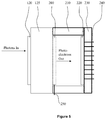
- FIG. 5 shows an imaging sensor incorporating a TANEA photocathode.
- the electron imager accepting the photoelectron flux may comprise an electron bombarded active pixel sensor (EBAPSTM) and EBCCD or other form of electron imager.
- EBAPSTM electron bombarded active pixel sensor
- EBCCD electron imager
- FIG. 6 shows a schematic representation of an image intensifier or a photomultiplier tube incorporating a TANEA photocathode. Note, independent of the image generated on the phosphor screen, the amplified electrical signal present on connection 370 meets the definition of a photomultiplier tube.
- TNEA thermally assisted negative electron affinity
- FIG. 1A illustrates a schematic of a thermally assisted negative electron affinity (NEA) according to one embodiment.
- the device comprises an optical window layer 105 , an optical absorber layer 110 , and a thermionic emission layer 115 .
- Table 1 further describes the active semiconductor layers of an embodiment of the thermally assisted negative electron affinity photocathode depicted schematically in FIG. 1A . The layers are listed in the order they are encountered by incoming light in a transmission mode structure.
- ARCs anti-reflection coatings
- a SiN x O y layer with an appropriate index of refraction and thickness can be used as an antireflection coating at the semiconductor—glass interface.
- a variety of coatings such as MgF may be used on the exposed glass surface.
- the photocathode must be brought into an effective negative electron affinity (NEA) state.
- NAA negative electron affinity
- the conventional nomenclature is used of referring to a cathode as being in an effective state of negative electron affinity if the undepleted portion of the conduction band of the barrier layer lies above the energy of a free electron in vacuum.
- a photocathode may be chemically cleaned, then given a vacuum thermal cycle in order to desorb any residual surface contaminants and finally coated with work function reducing materials such as, but not limited to, Rb+O 2 , Cs+O 2 or Cs+NF 3 .
- GaAs photocathode vacuum thermal cleaning process Details on a potential GaAs photocathode vacuum thermal cleaning process are found in U.S. Pat. No. 4,708,677. Semiconductor photocathode processing with cesium and oxygen was first described in U.S. Pat. No. 3,644,770. A more modern discussion of GaAs photocathode manufacturing methods are further detailed in a book written by Illes P. Csorba titled “Image Tubes”, copyright 1985, ISBN 0-672-22023-7. In the book, section 12.1.9.6 details “The Generation 3 Photocathode” Generation 3 image intensifiers use GaAs photocathodes similar to the prior art photocathode of FIG. 1B . The methods taught by Csorba are directly transferable to the structure disclosed in FIG. 1A .
- Csorba provides details on all of the major photocathode manufacturing steps from cathode growth through the deposition of a work-function lowering Cs+O 2 coating; to the extent that new materials are added in layer 115 , one skilled in the art may fine tune the described processes, if required, in order to achieve the desired results.
- GaAs photocathode activation physics is described in detail by: Applied Physics A: Materials Science & Processing (Historical Archive)
- Negative affinity 3-5 photocathodes Their physics and technology by W. E. Spicer, Issue: Volume 12, Number 2, Date: Feb. 1977 Pages: 115-130.
- FIG. 1A shows a schematic depiction of the active semiconductor layers which constitute a basic embodiment of the thermally assisted negative electron affinity (TANEA) photocathode.
- TNEA thermally assisted negative electron affinity
- Light may enter either side of the photocathode.
- the structure is often employed as a transmission mode photocathode. In the case of transmission mode operation, light will enter the photocathode through layer 105 .
- Layer 105 is a p-doped semiconductor layer where the bandgap of the semiconductor is larger than that of the p-doped semiconductor layer designated 110 .
- the doping and thickness of layer 105 are chosen such that several criteria are met.
- the thickness and the doping of layer 105 are chosen such that any transferred charge or interface states present on the surfaces of layer 105 are compensated by the p-type dopant without fully depleting the layer.
- the dopant level and thickness of layer 105 is chosen such that the un-depleted thickness of the layer is sufficient to prevent meaningful tunneling of charge to or from the conduction band of semiconductor layer 110 .
- Table 1 an Al 0.8 Ga 0.2 As layer p-doped to 6E18 cm ⁇ 3 at a thickness of 0.1 microns, meets these criteria.
- Layer 105 is often referred to as a window layer in that for a transmission mode application of the photocathode, light that has an energy falling below the bandgap energy of layer 105 may enter the photocathode with minimal absorption similar to light passing through an optical window.
- a semiconductor heterojunction is formed at the interface of layers 105 and 110 . Materials 105 and 110 are chosen such that the heterojunction provides a low interface recombination velocity for electrons residing in the conduction band of layer 110 .
- Layer 110 is a p-type semiconductor layer. The absorption coefficient and thickness of layer 110 typically determine the spectral response of the photocathode. Incident light transmitted through layer 105 is absorbed in layer 110 .
- Layer 110 is often referred to as an absorber layer.
- photoelectrons generated via the absorption of light in layer 110 are subsequently transported to the interface between layer 110 and 115 .
- the thickness and doping of layer 110 are typically chosen as a compromise between a number of factors. Those factors include the absorption coefficient for the wavelength range of interest, the temperature range of interest, the photoelectron (minority carrier) diffusion length and the energy difference between the Fermi level and the conduction band.
- the values quoted in Table 1 for layer 110 are reasonable choices for a room temperature photocathode designed to image at night under natural starlight conditions.
- Layer 115 is designed so as to result in a conduction band barrier when compared to layer 110 .
- This barrier may be introduced via an increase in the bandgap of layer 115 relative to layer 110 forming a heterojunction or by an increase in the p-type doping concentration of layer 115 relative to layer 110 or by a combination of these two methods.
- the heterojunction may be formed by a distinct atomically sharp transition or via a short ramp in the atomic constituents of the layer. Any ramp, if present, should be much shorter than the characteristic minority carrier diffusion length of the photoelectrons.
- Layer 115 may be referred to as a barrier layer due to the fact that the increase in the conduction band energy relative to layer 110 will generally decrease the efficiency of photoelectron transport toward the photoemission surface. In this embodiment, layer 115 also plays the role of the photoemission surface.
- Al X Ga (1-X) As a subset of the material family Al X Ga (1-X) As Y P (1-Y) has been shown to be easily controllable and therefore is favored as a practical embodiment for layer 115 .
- Al X Ga (1-X) As compositions where X is less than ⁇ 0.1% show little practical benefit over GaAs.
- Al X Ga (1-X) As compositions with X values greater than ⁇ 0.04 resulted in excessive photoelectron transport losses. Consequently, initial prototype photocathodes targeted X values ranging from ⁇ 0.001 to 0.04.
- the photocathode may be bonded to a support window.
- FIG. 2 schematically depicts the photocathode described in Table 1 after it has been anti-reflection coated and bonded to a transparent support substrate or window.
- the assembly is depicted as a transmission mode photocathode.
- the decision to employ this embodiment in a transmission mode photocathode is not meant as a limit on this disclosure, but rather just as one example.
- the disclosed structures will also yield performance benefits for reflection mode photocathodes.
- the first layer encountered by the light is an anti-reflection coating designated as 120 .
- Layer 120 may be a simple MgF 1 ⁇ 4-wave coating at the wavelength of interest or it may be a multi-layer coating designed for a specific set of targeted wavelengths or wavelength band. Alternatively, this layer may be omitted without impacting the intent of this disclosure.
- the second layer encountered by the incoming light is the transparent support substrate depicted as layer 125 .
- Layer 125 may be fabricated from Corning code 7056 glass or another transparent material. Corning code 7056 glass has been demonstrated to be a suitable support substrate for glass bonded GaAs based photocathodes.
- the next layer encountered by the incoming light is layer 130 .
- Layer 130 is an anti-reflection coating designed to minimize light loss as the incoming light transitions from layer 125 and enters the photocathode structure.
- Layer 130 may be formed from SiO x N y a material composed of silicon oxygen and nitrogen at a composition and thickness designed to achieve a minimum total reflection loss over the desired operational wavelength band of the photocathode.
- the first layer of the photocathode is layer 105 , the window layer.
- the window layer is designed to have a larger bandgap than the optical absorber layer 110 , both to allow light to pass easily through the window layer and to specify a low loss electron recombination velocity interface with the optical absorber layer.
- the light in the wavelength band of interest is primarily absorbed in layer 110 the optical absorber layer. Absorption of the light in layer 110 results in the generation of electron hole pairs where the electrons thermalize to the conduction band minimum reside of layer 110 . Diffusion transports the photoelectrons in the conduction band to the barrier layer ( 115 ) interface where the most energetic of the electrons in the thermalized electron energy distribution have a higher probability of diffusing across to the activation layer 135 . As the energetic electrons approach the interface between layer 115 and 135 , they will encounter an electric field that will tend to accelerate the electrons toward the vacuum lying beyond the surface of layer 135 . A significant fraction of the energetic electrons entering the activation layer will subsequently be emitted from the surface of the photocathode assembly. Layer 135 may be composed of Cesium and Oxygen. Methods of forming an efficient activation layer are well known to those skilled in the art. The exact composition of the activation layer is not material to the teaching of this disclosure.
- FIG. 3 is a schematic bandgap diagram of Thermally Assisted Negative Electron Affinity Photocathode containing an additional layer to modify photocathode surface chemistry.
- the alternate embodiment depicted in FIG. 3 interposed an additional emitter or emission layer between the thermionic barrier layer and the vacuum surface.
- the primary purpose of this layer is to specify a surface chemistry on the vacuum surface of the photocathode which is conducive to the formation of a stable, high efficiency activation layer.
- the photocathodes will exhibit a relatively high work function.
- the semiconductor surface In order to produce a surface that exhibits a high photoelectron escape probability, the semiconductor surface must first be cleaned to remove surface contaminants including native oxides. Numerous methods have been detailed in the literature to achieve an atomically clean surface including wet cleaning with HCl solutions to remove bulk surface oxides, heat cleaning to desorb residual oxides, adsorbed contaminants and atomic hydrogen cleaning.
- Aluminum oxide is a particularly difficult oxide to remove.
- the presence of aluminum oxide may interfere with the ability to form a high efficiency photocathode.
- a thin GaAs layer 140 may be formed over the barrier layer in order to eliminate the presence of native aluminum oxide on the surface of the photocathode.
- the use of thin GaAs surface layers does not negate the benefit of the thermionic emission barrier layer. Both doped as shown in Table 2 and intrinsic (non-intentionally doped) GaAs surface layers have been tested at thicknesses up to 10 nm with good results.
- the GaAs surface layer may be beneficial to incorporate in a thickness range between that of a single atomic layer up to a thickness of in excess of 30 nm.
- a work-function lowering coating such as Cs—O.
- any of the III-V semiconductor family of compounds may be used to design applicable TANEA photocathodes
- Group 5 elements that are specifically envisioned as being applicable include Aluminum, Gallium and Indium.
- Group 3 elements envisioned as suitable photocathode constituents include Nitrogen, Phosphorus, Arsenic and Antimony.
- FIG. 4B illustrates how a photocathode engineer may approach optimizing a TANEA photocathode for operation over a specific temperature range.
- the response versus barrier height curve will be different for each material system based on a wide range of material quality and interface properties.
- FIG. 5 is a schematic depiction of a vacuum image sensor incorporating a TANEA photocathode and an electron sensitive imager, such as an electron sensitive CMOS image sensor or an electron sensitive CCD.
- Layer 120 on the optical input surface is an anti-reflection coating as previously described in regards to FIG. 2 .
- 125 represents a transparent window (or substrate) as described in the FIG. 2 detailed description. In this case, the transparent window is used to form a portion of the vacuum envelope required to preserve a high level of sensitivity from the TANEA photocathode.
- the activation layer of the photocathode is particularly sensitive to contamination from oxygen, water and a wide variety of other trace gasses. In order to maintain clarity in FIGS.
- the volume depicted by 200 represents the sum of the layers previously described in FIG. 2 as the balance of the TANEA photocathode assembly. Specifically, layers 130 , 105 , 110 , 115 and 135 respectively as described in FIG. 2 are included and schematically represented as 200 . This description is not meant to restrict the choice of the photocathode engineer, an equally acceptable embodiment may include layers 140 as described in FIG. 3 between previously described layers 115 and 135 .
- Reference 210 represents that portion of the vacuum sensor body that makes up the side-walls of the sensor.
- Vacuum seals are formed on opposing surfaces of 210 in order to maintain a continuous unbroken vacuum envelope around the vacuum emission surface of the TANEA photocathode and the subsequent path of the emitted photoelectrons.
- 210 may be composed of a ceramic material such as Al 2 O 3 .
- 250 schematically represents an electrical connection from the outside of the vacuum envelope to the TANEA photocathode. The path of 250 is inconsequential to the intent of this disclosure as long as vacuum integrity is not compromised. An Ohmic contact between 250 and the semiconductor material of the TANEA photocathode is preferred.
- Reference 230 represents the vacuum enclosure completing the vacuum envelope opposite to the photocathode. This surface may be fabricated from a multi-layer ceramic block incorporating multiple electrical feedthroughs 240 . 230 additionally may be used to physically mount an electron imaging sensor 220 within the electron flux emitted from the TANEA photocathode assembly 200 .
- the electron sensitive image sensor 220 may constitute an electron bombarded active pixel sensor as detailed in U.S. Pat. No. 6,285,018. Similarly, 220 may be an electron bombarded CCD. It should also be noted that although the vacuum envelope side wall assembly 210 and the anode support surface of the vacuum enclosure 230 are depicted as separate objects, as detailed in U.S. Pat. No. 7,325,715, the side walls and anode support surfaces may be manufactured from a unitary ceramic assembly which includes all required electrical feedthroughs.
- FIG. 6 depicts a vacuum tube incorporating a TANEA photocathode that may be used either as a photomultiplier tube or as an image intensifier.
- the configuration of sensor schematically shown in FIG. 6 is commonly referred to as a proximity focused image intensifier.
- Proximity focused image intensifiers typically maintain image fidelity (as quantified by sensor modulation transfer function or MTF) by fabricating the sensor using the minimal practical vacuum gaps between the parallel planes of the photocathode, the MCP and the phosphor screen. Minimizing vacuum gaps results in increased acceleration field strength for emitted electrons which in turn minimizes electron time of flight.
- the practical limit to vacuum gap is typically set by manufacturing yield issues associated with increased electron emissions from the negatively biased surfaces when the sensor is not illuminated, primarily in the form of point source electron emissions.
- layer 120 on the optical input surface is an anti-reflection as previously described in regards to FIG. 2 .
- 125 represents a transparent window as described in the FIG. 2 detailed description.
- the transparent window is used to form a portion of the vacuum envelope required to preserve a high level of sensitivity from the TANEA photocathode.
- the activation layer of the photocathode is particularly sensitive to contamination from oxygen, water and a wide variety of other trace gasses.
- the volume depicted by 200 represents the sum of the layers previously described in FIG. 2 as the balance of the TANEA photocathode assembly.
- layers 130 , 105 , 110 , 115 and 135 respectively as described in FIG. 2 are included and schematically represented as 200 .
- This description is not meant to restrict the choice of the photocathode engineer, an equally acceptable embodiment may include layer 140 as described in FIG. 3 between previously described layers 115 and 135 .
- Reference 210 represents that portion of the vacuum sensor body that makes up the side-walls of the sensor. Vacuum seals are formed on opposing surfaces of 210 in order to maintain a continuous unbroken vacuum envelope around the vacuum emission surface of the TANEA photocathode and the subsequent path of the emitted photoelectrons.
- Side-wall 210 may be composed of a ceramic material such as Al 2 O 3 .
- Conductor 250 schematically represents an electrical connection from the outside of the vacuum envelope to the TANEA photocathode.
- a microchannel plate electron multiplier 310 is positioned inside the vacuum enclosure, facing the TANEA 200 .
- An electrical bias voltage is applied between the front and back surfaces of the microchannel plate (MCP) via contacts 350 and 360 respectively.
- Contacts 350 and 360 also schematically represent the physical support structure for the MCP.
- the MCP 310 When biased with an appropriate power supply, the MCP 310 will accept low level electron fluxes from the TANEA photocathode and multiply them by on the order of 1000 ⁇ while retaining the positional information associated with the incoming electron flux. Electron multiplication may be performed using a single MCP or a stack of MCP if higher gain values are required.
- the multiplied electron flux is then accelerated across a second vacuum gap defined by the output of the final MCP and surface 370 .
- Surface 370 is typically formed via a thin ( ⁇ 50 nm thick) Aluminum layer. Alternate conductive materials may be used to form surface 370 particularly when the tube is designed to be used as a photo-multiplier tube. In the case where the sensor will be used as an image intensifier, a thin layer of Aluminum is beneficial due to the relatively high transmission of thin Aluminum to electrons accelerated to a few kV. Electrons that successfully transit the layer 370 encounter phosphor layer 320 . When bombarded with electrons, phosphor layer 320 will generate an image that reproduces the photon image originally presented to the layer 200 TANEA photocathode assembly.
- Output window 340 may beneficially be made of any transparent material.
- Output window 340 may be composed of a fused fiber-optic bundle.
- Output window 340 and associated mounting flange 330 constitute a portion of the vacuum envelope of the vacuum tube.
- Mounting flange 330 is typically a conductive metal flange which serves to electrically connect the conductive surface 370 to external contact 380 .
- the sensor is biased by connecting various high voltage power supplies on contacts 250 , 350 , 360 and 380 . All transits of contacts through the vacuum envelope are generated in a leak-tight manner to ensure the vacuum integrity of the sensor.
Landscapes
- Physics & Mathematics (AREA)
- Electromagnetism (AREA)
- Common Detailed Techniques For Electron Tubes Or Discharge Tubes (AREA)
- Image-Pickup Tubes, Image-Amplification Tubes, And Storage Tubes (AREA)
Abstract
Description
| TABLE 1 | ||||
| Layer | Doping #/ | Thickness | Layer Title/ | |
| Number | Composition | cm3 | Microns | Function |
| 105 | Al0.8Ga0.2As | P-type, | 0.1 | Optical |
| 6 × 10¹⁸ | |
|||
| 110 | GaAs | P-type, | 2 | Optical |
| 3 × 10¹⁸ | | |||
| layer | ||||
| 115 | Al0.015Ga0.985As | P-type, | .03 | Thermionic |
| 7 × 10¹⁸ | Emission | |||
| Barrier Layer | ||||
| TABLE 2 | ||||
| Layer | Doping #/ | Thickness | Layer Title/ | |
| Number | Composition | cm3 | Microns | Function |
| 105 | Al0.8Ga0.2As | P-type, | 0.1 | Optical |
| 6 × 10¹⁸ | |
|||
| 110 | GaAs | P-type, | 2 | Optical |
| 3 × 10¹⁸ | | |||
| layer | ||||
| 115 | Al0.015Ga0.985As | P-type, | .03 | Thermionic |
| 7 × 10¹⁸ | | |||
| Barrier | ||||
| 140 | GaAs | P-type, | .005 | Surface |
| 7 × 10¹⁸ | Specification | |||
| Layer | ||||
| TABLE 3 | ||||
| Layer | Doping #/ | Thickness | Layer Title/ | |
| Number | Composition | cm3 | Microns | Function |
| 105 | Al0.8Ga0.185In0.015As | P-type, | 0.1 | Optical |
| 6 × 10¹⁸ | | |||
| Layer | ||||
| 110 | Ga0.985 In0.015As | P-type, | 2 | Optical |
| 3 × 10¹⁸ | | |||
| Layer | ||||
| 115 | GaAs or | P-type, | .03 | Thermionic |
| Al0.015Ga0.97In0.015As | 7 × 10¹⁸ | Emission | ||
| Barrier Layer | ||||
Claims (19)
Priority Applications (7)
| Application Number | Priority Date | Filing Date | Title |
|---|---|---|---|
| US15/702,647 US10692683B2 (en) | 2017-09-12 | 2017-09-12 | Thermally assisted negative electron affinity photocathode |
| EP18856829.9A EP3682461B1 (en) | 2017-09-12 | 2018-09-12 | Thermally assisted negative electron affinity photocathode |
| AU2018332878A AU2018332878B2 (en) | 2017-09-12 | 2018-09-12 | Thermally assisted negative electron affinity photocathode |
| IL273140A IL273140B2 (en) | 2017-09-12 | 2018-09-12 | Thermally assisted negative electron affinity photocathode |
| JP2020514947A JP7227230B2 (en) | 2017-09-12 | 2018-09-12 | Thermally assisted negative electron affinity photocathode |
| CA3075509A CA3075509C (en) | 2017-09-12 | 2018-09-12 | Thermally assisted negative electron affinity photocathode |
| PCT/US2018/050735 WO2019055554A1 (en) | 2017-09-12 | 2018-09-12 | Thermally assisted negative electron affinity photocathode |
Applications Claiming Priority (1)
| Application Number | Priority Date | Filing Date | Title |
|---|---|---|---|
| US15/702,647 US10692683B2 (en) | 2017-09-12 | 2017-09-12 | Thermally assisted negative electron affinity photocathode |
Publications (2)
| Publication Number | Publication Date |
|---|---|
| US20190080875A1 US20190080875A1 (en) | 2019-03-14 |
| US10692683B2 true US10692683B2 (en) | 2020-06-23 |
Family
ID=65632374
Family Applications (1)
| Application Number | Title | Priority Date | Filing Date |
|---|---|---|---|
| US15/702,647 Active US10692683B2 (en) | 2017-09-12 | 2017-09-12 | Thermally assisted negative electron affinity photocathode |
Country Status (7)
| Country | Link |
|---|---|
| US (1) | US10692683B2 (en) |
| EP (1) | EP3682461B1 (en) |
| JP (1) | JP7227230B2 (en) |
| AU (1) | AU2018332878B2 (en) |
| CA (1) | CA3075509C (en) |
| IL (1) | IL273140B2 (en) |
| WO (1) | WO2019055554A1 (en) |
Families Citing this family (1)
| Publication number | Priority date | Publication date | Assignee | Title |
|---|---|---|---|---|
| US11621289B2 (en) | 2020-05-22 | 2023-04-04 | Eotech, Llc | Compact proximity focused image sensor |
Citations (10)
| Publication number | Priority date | Publication date | Assignee | Title |
|---|---|---|---|---|
| US4829355A (en) * | 1985-12-20 | 1989-05-09 | Thomson-Csf | Photocathode having internal amplification |
| US5268612A (en) * | 1991-07-01 | 1993-12-07 | Intevac, Inc. | Feedback limited microchannel plate |
| US5349177A (en) * | 1993-02-22 | 1994-09-20 | Itt Corporation | Image intensifier tube having a solid state electron amplifier |
| US5712490A (en) * | 1996-11-21 | 1998-01-27 | Itt Industries, Inc. | Ramp cathode structures for vacuum emission |
| US6350999B1 (en) * | 1999-02-05 | 2002-02-26 | Matsushita Electric Industrial Co., Ltd. | Electron-emitting device |
| US6483231B1 (en) * | 1999-05-07 | 2002-11-19 | Litton Systems, Inc. | Night vision device and method |
| US20040084667A1 (en) * | 2001-03-27 | 2004-05-06 | Koji Takahashi | Semiconductor device and method of crystal growth |
| US20040104404A1 (en) * | 2002-11-26 | 2004-06-03 | Nec Compound Semiconductor Devices, Ltd. | Heterojunction field effect type semiconductor device having high gate turn-on voltage and low on-resistance and its manufacturing method |
| US20050106983A1 (en) * | 1999-03-18 | 2005-05-19 | Litton Systems, Inc. | Image intensification tube |
| US20070158638A1 (en) * | 2005-10-21 | 2007-07-12 | Perera A G U | Dual band photodetector |
Family Cites Families (10)
| Publication number | Priority date | Publication date | Assignee | Title |
|---|---|---|---|---|
| FR2507386A1 (en) * | 1981-06-03 | 1982-12-10 | Labo Electronique Physique | SEMICONDUCTOR DEVICE, ELECTRON TRANSMITTER, WITH ACTIVE LAYER HAVING A DOPING GRADIENT |
| JPH0512989A (en) * | 1991-07-01 | 1993-01-22 | Nec Corp | Semiconductor photo-electric surface and its manufacture |
| US5268570A (en) | 1991-12-20 | 1993-12-07 | Litton Systems, Inc. | Transmission mode InGaAs photocathode for night vision system |
| US5597112A (en) | 1994-10-13 | 1997-01-28 | Knapp; Frederick W. | Collapsible octahedral container |
| US6005257A (en) * | 1995-09-13 | 1999-12-21 | Litton Systems, Inc. | Transmission mode photocathode with multilayer active layer for night vision and method |
| JP2000090817A (en) * | 1998-09-11 | 2000-03-31 | Daido Steel Co Ltd | Polarized electron beam generator |
| US6633125B2 (en) * | 2001-05-31 | 2003-10-14 | Itt Manufacturing Enterprises, Inc. | Short wavelength infrared cathode |
| US6998635B2 (en) * | 2003-05-22 | 2006-02-14 | Itt Manufacturing Enterprises Inc. | Tuned bandwidth photocathode for transmission negative electron affinity devices |
| JP5267931B2 (en) | 2008-10-29 | 2013-08-21 | 独立行政法人理化学研究所 | Photocathode semiconductor device |
| US9601299B2 (en) * | 2012-08-03 | 2017-03-21 | Kla-Tencor Corporation | Photocathode including silicon substrate with boron layer |
-
2017
- 2017-09-12 US US15/702,647 patent/US10692683B2/en active Active
-
2018
- 2018-09-12 IL IL273140A patent/IL273140B2/en unknown
- 2018-09-12 WO PCT/US2018/050735 patent/WO2019055554A1/en not_active Ceased
- 2018-09-12 JP JP2020514947A patent/JP7227230B2/en active Active
- 2018-09-12 EP EP18856829.9A patent/EP3682461B1/en active Active
- 2018-09-12 AU AU2018332878A patent/AU2018332878B2/en active Active
- 2018-09-12 CA CA3075509A patent/CA3075509C/en active Active
Patent Citations (10)
| Publication number | Priority date | Publication date | Assignee | Title |
|---|---|---|---|---|
| US4829355A (en) * | 1985-12-20 | 1989-05-09 | Thomson-Csf | Photocathode having internal amplification |
| US5268612A (en) * | 1991-07-01 | 1993-12-07 | Intevac, Inc. | Feedback limited microchannel plate |
| US5349177A (en) * | 1993-02-22 | 1994-09-20 | Itt Corporation | Image intensifier tube having a solid state electron amplifier |
| US5712490A (en) * | 1996-11-21 | 1998-01-27 | Itt Industries, Inc. | Ramp cathode structures for vacuum emission |
| US6350999B1 (en) * | 1999-02-05 | 2002-02-26 | Matsushita Electric Industrial Co., Ltd. | Electron-emitting device |
| US20050106983A1 (en) * | 1999-03-18 | 2005-05-19 | Litton Systems, Inc. | Image intensification tube |
| US6483231B1 (en) * | 1999-05-07 | 2002-11-19 | Litton Systems, Inc. | Night vision device and method |
| US20040084667A1 (en) * | 2001-03-27 | 2004-05-06 | Koji Takahashi | Semiconductor device and method of crystal growth |
| US20040104404A1 (en) * | 2002-11-26 | 2004-06-03 | Nec Compound Semiconductor Devices, Ltd. | Heterojunction field effect type semiconductor device having high gate turn-on voltage and low on-resistance and its manufacturing method |
| US20070158638A1 (en) * | 2005-10-21 | 2007-07-12 | Perera A G U | Dual band photodetector |
Non-Patent Citations (1)
| Title |
|---|
| International Preliminary Report on Patentability for PCT/US2018/050735, filed Sep. 12, 2018, dated Mar. 17, 2020, 12 pages. |
Also Published As
| Publication number | Publication date |
|---|---|
| EP3682461B1 (en) | 2024-11-06 |
| CA3075509C (en) | 2024-05-14 |
| IL273140B1 (en) | 2024-06-01 |
| AU2018332878A1 (en) | 2020-04-09 |
| JP2020533760A (en) | 2020-11-19 |
| IL273140B2 (en) | 2024-10-01 |
| WO2019055554A1 (en) | 2019-03-21 |
| JP7227230B2 (en) | 2023-02-21 |
| AU2018332878B2 (en) | 2023-03-30 |
| IL273140A (en) | 2020-04-30 |
| EP3682461A4 (en) | 2021-11-10 |
| CA3075509A1 (en) | 2019-03-21 |
| US20190080875A1 (en) | 2019-03-14 |
| EP3682461A1 (en) | 2020-07-22 |
Similar Documents
| Publication | Publication Date | Title |
|---|---|---|
| Martinelli et al. | The application of semiconductors with negative electron affinity surfaces to electron emission devices | |
| US8558234B2 (en) | Low voltage low light imager and photodetector | |
| Williams et al. | Current status of negative electron affinity devices | |
| US5747826A (en) | Photoemitter electron tube, and photodetector | |
| US4280074A (en) | Collector for thermionic energy converter | |
| US7030406B2 (en) | Semiconductor photocathode and photoelectric tube using the same | |
| JP3524249B2 (en) | Electron tube | |
| Escher et al. | Field-assisted semiconductor photoemitters for the 1—2-µm range | |
| US6836059B2 (en) | Image intensifier and electron multiplier therefor | |
| Seib et al. | Photodetectors for the 0.1 to 1.0 μm Spectral Region | |
| US10692683B2 (en) | Thermally assisted negative electron affinity photocathode | |
| US5712490A (en) | Ramp cathode structures for vacuum emission | |
| JP3565526B2 (en) | Photoemission surface and electron tube using the same | |
| JPH11135003A (en) | Photoelectric surface and electron tube using it | |
| JP3615856B2 (en) | Photoelectric surface and photoelectric conversion tube using the same | |
| US6563264B2 (en) | Photocathode and electron tube | |
| US20090273281A1 (en) | Photocathode and electron tube having the same | |
| Zwicker | Photoemissive detectors | |
| JPH1196897A (en) | Photoelectric cathode and electron tube using the same | |
| JPH09213204A (en) | Photoelectric surface and electronic tube using the photoelectric surface | |
| Aebi et al. | Near IR photocathode development | |
| Fu et al. | Study on spectral response characteristics of NEA GaAlAs/GaAs vacuum photodiode based on external electric field | |
| Nikzad et al. | Low Voltage Low Light Imager and Photodetector |
Legal Events
| Date | Code | Title | Description |
|---|---|---|---|
| FEPP | Fee payment procedure |
Free format text: ENTITY STATUS SET TO UNDISCOUNTED (ORIGINAL EVENT CODE: BIG.); ENTITY STATUS OF PATENT OWNER: SMALL ENTITY |
|
| FEPP | Fee payment procedure |
Free format text: ENTITY STATUS SET TO SMALL (ORIGINAL EVENT CODE: SMAL); ENTITY STATUS OF PATENT OWNER: SMALL ENTITY |
|
| AS | Assignment |
Owner name: INTEVAC, INC., CALIFORNIA Free format text: ASSIGNMENT OF ASSIGNORS INTEREST;ASSIGNORS:COSTELLO, KENNETH A.;AEBI, VERLE W.;JURKOVIC, MICHAEL;AND OTHERS;SIGNING DATES FROM 20171016 TO 20171110;REEL/FRAME:044156/0276 |
|
| STPP | Information on status: patent application and granting procedure in general |
Free format text: RESPONSE TO NON-FINAL OFFICE ACTION ENTERED AND FORWARDED TO EXAMINER |
|
| STPP | Information on status: patent application and granting procedure in general |
Free format text: FINAL REJECTION MAILED |
|
| STPP | Information on status: patent application and granting procedure in general |
Free format text: DOCKETED NEW CASE - READY FOR EXAMINATION |
|
| STPP | Information on status: patent application and granting procedure in general |
Free format text: NON FINAL ACTION MAILED |
|
| STPP | Information on status: patent application and granting procedure in general |
Free format text: NOTICE OF ALLOWANCE MAILED -- APPLICATION RECEIVED IN OFFICE OF PUBLICATIONS |
|
| STPP | Information on status: patent application and granting procedure in general |
Free format text: PUBLICATIONS -- ISSUE FEE PAYMENT VERIFIED |
|
| STCF | Information on status: patent grant |
Free format text: PATENTED CASE |
|
| AS | Assignment |
Owner name: BLUE TORCH FINANCE LLC, NEW YORK Free format text: PATENT SECURITY AGREEMENT;ASSIGNORS:EOTECH, LLC;HEL TECHNOLOGIES, LLC;REEL/FRAME:058600/0351 Effective date: 20211230 |
|
| AS | Assignment |
Owner name: EOTECH, LLC, MICHIGAN Free format text: ASSIGNMENT OF ASSIGNORS INTEREST;ASSIGNOR:INTEVAC, INC;REEL/FRAME:058589/0494 Effective date: 20211230 |
|
| AS | Assignment |
Owner name: BLUE TORCH FINANCE LLC, AS ADMINISTRATIVE AGENT, NEW YORK Free format text: PATENT SECURITY AGREEMENT;ASSIGNOR:EOTECH, LLC;REEL/FRAME:059725/0564 Effective date: 20211230 |
|
| AS | Assignment |
Owner name: HEL TECHNOLOGIES, LLC, MICHIGAN Free format text: NOTICE OF RELEASE OF SECURITY INTEREST IN PATENT COLLATERAL;ASSIGNOR:BLUE TORCH FINANCE LLC, AS COLLATERAL AGENT;REEL/FRAME:064356/0155 Effective date: 20230721 Owner name: EOTECH, LLC, MICHIGAN Free format text: NOTICE OF RELEASE OF SECURITY INTEREST IN PATENT COLLATERAL;ASSIGNOR:BLUE TORCH FINANCE LLC, AS COLLATERAL AGENT;REEL/FRAME:064356/0155 Effective date: 20230721 |
|
| AS | Assignment |
Owner name: KEYBANK NATIONAL ASSOCIATION, AS ADMINISTRATIVE AGENT, OHIO Free format text: SECURITY INTEREST;ASSIGNOR:EOTECH, LLC;REEL/FRAME:064571/0724 Effective date: 20230721 |
|
| MAFP | Maintenance fee payment |
Free format text: PAYMENT OF MAINTENANCE FEE, 4TH YR, SMALL ENTITY (ORIGINAL EVENT CODE: M2551); ENTITY STATUS OF PATENT OWNER: SMALL ENTITY Year of fee payment: 4 |
|
| AS | Assignment |
Owner name: PHOTONICS WEST, LLC, MICHIGAN Free format text: ASSIGNMENT OF ASSIGNORS INTEREST;ASSIGNOR:EOTECH, LLC;REEL/FRAME:068644/0238 Effective date: 20240827 |
|
| AS | Assignment |
Owner name: PHOTONICS WEST, LLC, MICHIGAN Free format text: CORRECTIVE ASSIGNMENT TO CORRECT THE THE APPLICATION NUMBER INCORRECTLY LISTED AS PATENT NUMBER PREVIOUSLY RECORDED AT REEL: 68644 FRAME: 238. ASSIGNOR(S) HEREBY CONFIRMS THE ASSIGNMENT;ASSIGNOR:EOTECH, LLC;REEL/FRAME:069057/0092 Effective date: 20240827 |
|
| AS | Assignment |
Owner name: KEYBANK NATIONAL ASSOCIATION, AS ADMINISTRATIVE AGENT, OHIO Free format text: SECURITY INTEREST;ASSIGNOR:PHOTONICS WEST, LLC;REEL/FRAME:069110/0610 Effective date: 20241001 |