EP3660185A1 - Verfahren zur synthetisierung einer kupfer-silber-legierung, verfahren zur formung eines leitungsteils, kupfer-silber-legierung und leitungsteil - Google Patents
Verfahren zur synthetisierung einer kupfer-silber-legierung, verfahren zur formung eines leitungsteils, kupfer-silber-legierung und leitungsteil Download PDFInfo
- Publication number
- EP3660185A1 EP3660185A1 EP18838388.9A EP18838388A EP3660185A1 EP 3660185 A1 EP3660185 A1 EP 3660185A1 EP 18838388 A EP18838388 A EP 18838388A EP 3660185 A1 EP3660185 A1 EP 3660185A1
- Authority
- EP
- European Patent Office
- Prior art keywords
- copper
- silver
- peak
- silver alloy
- crystal
- Prior art date
- Legal status (The legal status is an assumption and is not a legal conclusion. Google has not performed a legal analysis and makes no representation as to the accuracy of the status listed.)
- Pending
Links
Images

Classifications
-
- H—ELECTRICITY
- H01—ELECTRIC ELEMENTS
- H01B—CABLES; CONDUCTORS; INSULATORS; SELECTION OF MATERIALS FOR THEIR CONDUCTIVE, INSULATING OR DIELECTRIC PROPERTIES
- H01B1/00—Conductors or conductive bodies characterised by the conductive materials; Selection of materials as conductors
- H01B1/02—Conductors or conductive bodies characterised by the conductive materials; Selection of materials as conductors mainly consisting of metals or alloys
- H01B1/026—Alloys based on copper
-
- C—CHEMISTRY; METALLURGY
- C09—DYES; PAINTS; POLISHES; NATURAL RESINS; ADHESIVES; COMPOSITIONS NOT OTHERWISE PROVIDED FOR; APPLICATIONS OF MATERIALS NOT OTHERWISE PROVIDED FOR
- C09D—COATING COMPOSITIONS, e.g. PAINTS, VARNISHES OR LACQUERS; FILLING PASTES; CHEMICAL PAINT OR INK REMOVERS; INKS; CORRECTING FLUIDS; WOODSTAINS; PASTES OR SOLIDS FOR COLOURING OR PRINTING; USE OF MATERIALS THEREFOR
- C09D11/00—Inks
- C09D11/02—Printing inks
- C09D11/03—Printing inks characterised by features other than the chemical nature of the binder
- C09D11/037—Printing inks characterised by features other than the chemical nature of the binder characterised by the pigment
-
- C—CHEMISTRY; METALLURGY
- C09—DYES; PAINTS; POLISHES; NATURAL RESINS; ADHESIVES; COMPOSITIONS NOT OTHERWISE PROVIDED FOR; APPLICATIONS OF MATERIALS NOT OTHERWISE PROVIDED FOR
- C09D—COATING COMPOSITIONS, e.g. PAINTS, VARNISHES OR LACQUERS; FILLING PASTES; CHEMICAL PAINT OR INK REMOVERS; INKS; CORRECTING FLUIDS; WOODSTAINS; PASTES OR SOLIDS FOR COLOURING OR PRINTING; USE OF MATERIALS THEREFOR
- C09D11/00—Inks
- C09D11/52—Electrically conductive inks
-
- C—CHEMISTRY; METALLURGY
- C22—METALLURGY; FERROUS OR NON-FERROUS ALLOYS; TREATMENT OF ALLOYS OR NON-FERROUS METALS
- C22C—ALLOYS
- C22C1/00—Making non-ferrous alloys
-
- C—CHEMISTRY; METALLURGY
- C23—COATING METALLIC MATERIAL; COATING MATERIAL WITH METALLIC MATERIAL; CHEMICAL SURFACE TREATMENT; DIFFUSION TREATMENT OF METALLIC MATERIAL; COATING BY VACUUM EVAPORATION, BY SPUTTERING, BY ION IMPLANTATION OR BY CHEMICAL VAPOUR DEPOSITION, IN GENERAL; INHIBITING CORROSION OF METALLIC MATERIAL OR INCRUSTATION IN GENERAL
- C23C—COATING METALLIC MATERIAL; COATING MATERIAL WITH METALLIC MATERIAL; SURFACE TREATMENT OF METALLIC MATERIAL BY DIFFUSION INTO THE SURFACE, BY CHEMICAL CONVERSION OR SUBSTITUTION; COATING BY VACUUM EVAPORATION, BY SPUTTERING, BY ION IMPLANTATION OR BY CHEMICAL VAPOUR DEPOSITION, IN GENERAL
- C23C18/00—Chemical coating by decomposition of either liquid compounds or solutions of the coating forming compounds, without leaving reaction products of surface material in the coating; Contact plating
- C23C18/02—Chemical coating by decomposition of either liquid compounds or solutions of the coating forming compounds, without leaving reaction products of surface material in the coating; Contact plating by thermal decomposition
- C23C18/08—Chemical coating by decomposition of either liquid compounds or solutions of the coating forming compounds, without leaving reaction products of surface material in the coating; Contact plating by thermal decomposition characterised by the deposition of metallic material
-
- C—CHEMISTRY; METALLURGY
- C23—COATING METALLIC MATERIAL; COATING MATERIAL WITH METALLIC MATERIAL; CHEMICAL SURFACE TREATMENT; DIFFUSION TREATMENT OF METALLIC MATERIAL; COATING BY VACUUM EVAPORATION, BY SPUTTERING, BY ION IMPLANTATION OR BY CHEMICAL VAPOUR DEPOSITION, IN GENERAL; INHIBITING CORROSION OF METALLIC MATERIAL OR INCRUSTATION IN GENERAL
- C23C—COATING METALLIC MATERIAL; COATING MATERIAL WITH METALLIC MATERIAL; SURFACE TREATMENT OF METALLIC MATERIAL BY DIFFUSION INTO THE SURFACE, BY CHEMICAL CONVERSION OR SUBSTITUTION; COATING BY VACUUM EVAPORATION, BY SPUTTERING, BY ION IMPLANTATION OR BY CHEMICAL VAPOUR DEPOSITION, IN GENERAL
- C23C18/00—Chemical coating by decomposition of either liquid compounds or solutions of the coating forming compounds, without leaving reaction products of surface material in the coating; Contact plating
- C23C18/14—Decomposition by irradiation, e.g. photolysis, particle radiation or by mixed irradiation sources
- C23C18/143—Radiation by light, e.g. photolysis or pyrolysis
-
- C—CHEMISTRY; METALLURGY
- C23—COATING METALLIC MATERIAL; COATING MATERIAL WITH METALLIC MATERIAL; CHEMICAL SURFACE TREATMENT; DIFFUSION TREATMENT OF METALLIC MATERIAL; COATING BY VACUUM EVAPORATION, BY SPUTTERING, BY ION IMPLANTATION OR BY CHEMICAL VAPOUR DEPOSITION, IN GENERAL; INHIBITING CORROSION OF METALLIC MATERIAL OR INCRUSTATION IN GENERAL
- C23C—COATING METALLIC MATERIAL; COATING MATERIAL WITH METALLIC MATERIAL; SURFACE TREATMENT OF METALLIC MATERIAL BY DIFFUSION INTO THE SURFACE, BY CHEMICAL CONVERSION OR SUBSTITUTION; COATING BY VACUUM EVAPORATION, BY SPUTTERING, BY ION IMPLANTATION OR BY CHEMICAL VAPOUR DEPOSITION, IN GENERAL
- C23C26/00—Coating not provided for in groups C23C2/00 - C23C24/00
-
- H—ELECTRICITY
- H01—ELECTRIC ELEMENTS
- H01B—CABLES; CONDUCTORS; INSULATORS; SELECTION OF MATERIALS FOR THEIR CONDUCTIVE, INSULATING OR DIELECTRIC PROPERTIES
- H01B1/00—Conductors or conductive bodies characterised by the conductive materials; Selection of materials as conductors
- H01B1/20—Conductive material dispersed in non-conductive organic material
- H01B1/22—Conductive material dispersed in non-conductive organic material the conductive material comprising metals or alloys
-
- H—ELECTRICITY
- H01—ELECTRIC ELEMENTS
- H01B—CABLES; CONDUCTORS; INSULATORS; SELECTION OF MATERIALS FOR THEIR CONDUCTIVE, INSULATING OR DIELECTRIC PROPERTIES
- H01B13/00—Apparatus or processes specially adapted for manufacturing conductors or cables
-
- H—ELECTRICITY
- H05—ELECTRIC TECHNIQUES NOT OTHERWISE PROVIDED FOR
- H05K—PRINTED CIRCUITS; CASINGS OR CONSTRUCTIONAL DETAILS OF ELECTRIC APPARATUS; MANUFACTURE OF ASSEMBLAGES OF ELECTRICAL COMPONENTS
- H05K3/00—Apparatus or processes for manufacturing printed circuits
- H05K3/10—Apparatus or processes for manufacturing printed circuits in which conductive material is applied to the insulating support in such a manner as to form the desired conductive pattern
- H05K3/12—Apparatus or processes for manufacturing printed circuits in which conductive material is applied to the insulating support in such a manner as to form the desired conductive pattern using thick film techniques, e.g. printing techniques to apply the conductive material or similar techniques for applying conductive paste or ink patterns
-
- C—CHEMISTRY; METALLURGY
- C22—METALLURGY; FERROUS OR NON-FERROUS ALLOYS; TREATMENT OF ALLOYS OR NON-FERROUS METALS
- C22C—ALLOYS
- C22C5/00—Alloys based on noble metals
- C22C5/06—Alloys based on silver
- C22C5/08—Alloys based on silver with copper as the next major constituent
-
- C—CHEMISTRY; METALLURGY
- C22—METALLURGY; FERROUS OR NON-FERROUS ALLOYS; TREATMENT OF ALLOYS OR NON-FERROUS METALS
- C22C—ALLOYS
- C22C9/00—Alloys based on copper
Definitions
- the present invention relates to a method for synthesizing a copper-silver alloy by which a copper-silver alloy can be easily synthesized at a low temperature in a short time period, and to a method for forming a conduction part, a copper-silver alloy, and a conduction part.
- wearable devices are rapidly developed. Wearable devices are supposed to be utilized in the state of being worn on a body, and are required to be reduced in size or thickness. Electronic components for use in these devices are also required to satisfy similar requirements so as to meet that requirement. Since size and thickness reductions in the electronic components are accompanied with a decrease in heat resistance, wiring materials which can be formed by a simple process, such as short-time heating or low-temperature bonding, have been proposed. Electroconductive inks such as copper inks, silver inks, and copper-silver inks are used for these wiring materials, and investigations are being made on electroconductive inks and techniques for forming wiring using the electroconductive ink.
- Patent Literature 1 proposes a method for producing an electroconductive portion including copper as a main component, the method being capable of forming the electroconductive portion at a low temperature region such that resins can be utilized as base materials.
- Patent Literature 1 discloses that, in the production method described therein, a copper ink is printed on a substrate and then heat-treated for 10 minutes to 60 minutes at a temperature range of 60°C to 300°C.
- Patent Literature 1 further discloses an ink composition including: a copper salt composed of carboxylic acids having a reducing function and copper ions; a coordinating compound for stabilizing the reducing function; and metallic silver or a silver metalcarboxylate for enhancing the reducing function.
- Patent Literature 1 describes in Example 7 that an ink composition including fine particles of copper salts, hexamethylimine, and fine particles of silver is prepared and applied to a base material and thereafter the base material is heat-treated at 140°C for 30 minutes in an atmosphere through which nitrogen gas is passing, thereby forming a conduction part.
- Patent Literature 2 discloses a method for electroconductive-pattern formation for efficiently making a pattern of a composition printed on a substrate electroconductive.
- a composition including metal oxide particles having a flat shape, a reducing agent, and a binder resin is used and the composition is irradiated with pulsed light or microwaves.
- Patent Literature 2 discloses, as the method for electroconductive-pattern formation described therein, a method in which a paste obtained by mixing flat copper oxide particles, a reducing agent, and a resin is printed on a substrate and the printed paste is irradiated with a single-shot pulse wave under the conditions of a voltage of 250 V, a pulse width of 1,600 ⁇ s, and a pulse energy of 3.47 J/cm 2 .
- Patent Literature 3 discloses a method for producing a copper-silver alloy containing no copper-silver eutectoid. Specifically, Patent Literature 3 discloses a production method in which a fluid containing copper ions and silver ions is mixed with a fluid containing a reducing agent to thereby precipitate copper-silver alloy particles having a particle diameter of 50 nm or less and containing no eutectoid. Although Patent Literature 3 does not clearly describe any means for forming a conduction part on a substrate, Patent Literature 3 describes that since the copper-silver alloy powder having a particle diameter of 50 nm or less is used, circuits can be formed on plastic substrates by a low-temperature coating and sintering process.
- Non-Patent Literature 1 edited and written by Seizo NAGASAKI and Makoto HIRABAYASHI, "Binary Alloy Phase Diagrams", AGNE Gijutsu Center Inc., May 30, 2013, p.4
- Patent Literature 1 the heat treatment time and the heat treatment temperature are specified for the purposes of volatilizing off the coordinating compound and reducing the copper ions.
- Patent Literature 1 describes that, in order to achieve the purposes, fine particles of a composite of the metal particles or metal salt, which is for accelerating the reduction of copper ions, with fine particles of copper salt are not formed. Consequently, the invention described in Patent Literature 1 does not employ any compositing method such as a method for alloying the two kinds of particles.
- Patent Literature 1 describes that an electroconductive member made of copper can be formed by merely performing a heat treatment for 10 minutes to 60 minutes at a temperature range of 60°C to 300°C. These heating conditions can hence be regarded as conditions under which the fine copper particles are not alloyed with the fine silver particles. Consequently, the conduction member obtained by the production method described in Patent Literature 1, which is made of copper, has a problem that increase in resistivity of this conductive member is caused by oxidation.
- Patent Literature 2 may be efficient only with respect to the step of making the composition for conductive-patter formation electroconductive, but flat oxide particles, a reducing agent, and a resin must be prepared.
- Patent Literature 2 describes only a method for producing flat oxide particles, and it is unclear whether flat particles of other metal oxides are obtained by the same method. In a case where particles of a metal oxide are obtained only as spherical particles, these particles must be made flat with a ball mill or the like, resulting in complicated production process. Meanwhile, the irradiation with pulsed light in Patent Literature 2 is intended to remove oxides present on the surface of the particles, together with the reducing agent.
- Patent Literature 2 hence describes that metallic particles of an alloy may also be used, copper alloy formation with pulsed light is not supposed therein at all. Consequently, the conduction member obtained by the production method described in Patent Literature 2 includes copper as a main component and hence has a problem that increase in resistivity of this conduction member is caused by oxidation, as in Patent Literature 1.
- Patent Literatures 2 and 3 necessitate use of a special reducing agent, making it difficult to reduce the production cost.
- an object of the present invention is to provide a method for synthesizing a copper-silver alloy by which a copper-silver alloy can be easily synthesized at a low temperature in a short time period, a method for forming a conduction part, a copper-silver alloy, and a conduction part.
- the present inventors conducted investigation on the premise that a copper-silver alloy is used in order to avoid the problem of oxidation associated with copper and the problem of migration associated with silver.
- the present inventors directed attention to the behavior of copper-silver alloys during sintering in order to form a copper-silver alloy without using a reducing agent as in Patent Literature 3.
- the present inventors found that, after fine crystal nuclei of silver and copper were formed, the diffusion and growth of copper and silver occurred from the crystal nuclei as starting points, thereby forming a copper-silver alloy.
- Examples of common methods for producing a copper-silver alloy include an atomization method and the like besides the high-temperature melting method and liquid-phase reduction method described above. However, these methods each employ a high-temperature treatment and necessitate a complicated process. The method in which a reducing agent is used has problems of increase in cost and the like. It is hence difficult to apply any of these common methods to flexible substrates or components which have low heat resistance.
- the present inventors directing attention to formation of fine crystal nuclei of silver and copper and synthesis of a copper-silver alloy therefrom, dared to make investigations on a synthesis method based on heating performed at a low temperature for a short time period.
- the present inventors added a silver salt as fine silver particles to thereby evenly disperse the particles in an ink and yielded fine crystal nuclei of metallic copper and metallic silver by conducting heating at a given temperature for a given time period.
- This method is unable to alloy copper with silver under the conditions applicable to wearable devices, like the method described in Patent Literature 1. Although it may be thought that to conduct heating at a low temperature for a long period of time is effective in alloying, such long-period heating is undesirable from the standpoint of production process simplification. Even when a reduction method is used, complicated processes are necessary for reducing the difference in oxidation-reduction potential between copper and silver.
- the present inventors yielded crystal nuclei of copper and silver at a low temperature and thereafter irradiated these crystal nuclei with pulsed light having a given energy density, which had been commonly used for removing oxide films, purposely for a short time period.
- these crystal nuclei were synthesized by the irradiation and a copper-silver alloy was formed.
- the resultant copper-silver alloy has a homogeneous structure, making it possible to reduce the resistance of conduction parts.
- the copper-silver alloy obtained by such a synthesis method has a crystal grain diameter of 0.1 ⁇ m or less and satisfies at least one of a requirement that a difference between a peak of (111) plane angle of the Cu and a peak of (111) plane angle of pure Cu is at least 0.3% of the peak of (111) plane angle of the pure Cu and a requirement that a difference between a peak of (111) plane angle of the Ag and a peak of (111) plane angle of pure Ag is at least 0.1% of the peak of (111) plane angle of the pure Ag.
- the present inventors have further found that the crystal nuclei of copper can be inhibited from oxidizing by optimizing the conditions for forming the crystal nuclei. Furthermore, the present inventors have found that, by optimizing the conditions for forming the crystal nuclei, a copper-silver alloy can be synthesized in a short time period and the crystal nuclei can be inhibited from flying off.
- the method for synthesizing a copper-silver alloy in the present invention includes (1) an ink preparation step of mixing a copper salt particle, an amine-based solvent, and a silver salt particle, thereby preparing a copper-silver ink, (2) a coating step of coating a member to be coated with the copper-silver ink, (3) a crystal nucleus formation step of forming at least one of a crystal nucleus of copper having a crystal grain diameter of 0.2 ⁇ m or less and a crystal nucleus of silver having a crystal grain diameter of 0.2 ⁇ m or less from the copper-silver ink, and (4) a crystal nucleus synthesis step of synthesizing the crystal nucleus of copper and the crystal nucleus of silver.
- an ink preparation step of mixing a copper salt particle, an amine-based solvent, and a silver salt particle, thereby preparing a copper-silver ink
- a coating step of coating a member to be coated with the copper-silver ink
- the copper salt used in the synthesis method in the present invention is composed of acids and copper ions.
- the acid is not particularly limited so long as the salt is soluble in the amine-based solvent.
- a copper carboxylate is desirable.
- the copper carboxylate include fine particles of copper formate, fine particles of copper hydroxyacetate, fine particles of copper glyoxylate, fine particles of copper lactate, fine particles of copper oxalate, fine particles of copper tartrate, fine particles of copper malate, and fine particles of copper citrate.
- copper formate particles are preferred from the standpoint of low cost.
- One of these copper salts may be used alone, or two or more thereof may be used in combination. In the case of using two or more thereof in combination, these copper salts may be mixed in any desired proportion.
- the copper ion may be any of the mono- to trivalent copper ions.
- the average primary-particle diameter of the copper salt particles are not particularly limited, because the copper salt particles dissolve in the amine-based solvent.
- the copper salt particles used in the present invention are not particularly limited, and may be commercial ones or may be ones synthesized by a comment method. Methods for production thereof are also not particularly limited.
- the amine-based solvent used in the synthesis method in the present invention is not particularly limited.
- aliphatic amines, aromatic amines, and cyclic amines are preferred from the standpoints that the copper salt particles and the silver salt particles described below readily dissolve therein and that the amine-based solvent can be easily removed in forming conduction parts.
- Examples of the aliphatic amines include alkylamines, alkanolamines, alkylenediamines, cyclic amines, and amidine compounds. Preferred of these is 2-ethylhexylamine.
- Examples of the aromatic amines include aniline, p-toluidine, 4-ethylaniline, N-methylaniline, N-methyl-p-toluidine, and N-methyl-4-ethylaniline.
- Examples of the cyclic amines include pyrrolidine, pyrrole, piperidine, pyridine, hexamethyleneimine, imidazole, pyrazole, piperazine, N-methylpiperazine, N-ethylpiperazine, and homopiperazine.
- the amine-based solvent may be a commercial one or may be one synthesized by a common method.
- the silver salt used in the synthesis method in the present invention is composed of acids and silver ions.
- the acid is not particularly limited so long as the salt is soluble in the amine-based solvent.
- a carboxylic acid is desirable.
- a silver ⁇ -ketocarboxylate is preferable from the standpoint of reducing the concentration of any raw material and impurities remaining in the formation of metallic silver.
- silver ⁇ -ketocarboxylate examples include silver 2-methylacetoacetate, silver acetoacetate, silver 2-ethylacetoacetate, silver propionylacetate, silver isobutyrylacetate, silver pivaloylacetate, silver caproylacetate, silver 2-n-butylacetoacetate, silver 2-benzylacetoacetate, silver benzoylacetate, silver pivaloylacetoacetate, silver rylacetoacetate, silver 2-acetylpivaloylacetate, silver 2-acetylisobutyrylacetate, and silver acetonedicarboxylate.
- the average primary-particle diameter of the silver salt particles is not particularly limited, like the average primary-particle diameter of the copper salt particles, because the silver salt particles dissolve in the amine-based solvent.
- One kind of silver salt particles may be used alone, or two or more kinds of silver salt particles may be used in combination. In the case of using two or more kinds of silver salt particles in combination, the two kinds of particles may be mixed in any desired proportion.
- the copper salt particles used in the present invention are not particularly limited, and may be commercial ones or may be ones synthesized by a common method. Methods for production thereof are also not particularly limited.
- the mixing ratio between the copper salt particles and the silver salt particles it is preferred to mix the two kinds of particles so as to result in a copper/silver ratio of 5/95 to 95/5 after sintering. So long as the mixing ratio is within that range, oxidation and migration can be inhibited, and oxidation during heating and migration during heating can be inhibited.
- the total content of the copper salt particles and the silver salt particles is preferably 5% by mass to 95% by mass based on the total mass of the copper-silver ink.
- the content of the amine-based solvent is preferably 5% by mass to 50% by mass based on the total mass of the copper-silver ink.
- the copper-silver ink may further contain at least one of alcohols such as methanol and ethanol, ethers such as diethyl ether, esters such as methyl formate, aliphatic hydrocarbons such as n-hexane, and aromatic hydrocarbons such as benzene.
- the content of such a dispersion medium is preferably 0% by mass to 90% by mass based on the total mass of the copper-silver ink.
- a suitable method may be selected from common methods such as a mixing method by rotating a stirrer, stirring blades or the like, a mixing method using a mixer, three-roll mill, kneader, bead mill or the like, and a mixing method by ultrasonic waves.
- the copper-silver ink by adding a given amount of a copper salt to an amine-based solvent, mixing them, thereafter adding a given amount of a silver salt thereto, and then mixing them.
- the temperature during the mixing is not particularly limited so long as the ingredients do not deteriorate, and the temperature is preferably -5°C to 60°C. It is desirable that the temperature during the mixing is suitably regulated depending on the kinds and amounts of the ingredients so that the mixture obtained by mixing the ingredients has a viscosity suitable for stirring.
- the mixing time is not particularly limited so long as the ingredients for the copper-silver ink do not deteriorate.
- the mixing time is preferably 10 minutes to 1 hour.
- the viscosity of the copper-silver ink obtained by the mixing may be any viscosity which renders the ink printable, and is suitably regulated depending on coating methods.
- methods for coating a base material with the copper-silver ink are not particularly limited, and common methods may be used. Examples thereof include screen printing, dip coating, spray coating, spin coating, ink-jet printing, and application with a dispenser.
- the shape of coating ink is not particularly limited, and the shape of coating ink may be either a planar shape or a dot arrangement without arousing any problem.
- the amount of the copper-silver ink with which the base material is coated may be suitably regulated depending on the desired thickness of the conduction part.
- the member to be coated may be either a solid or a liquid or a gas.
- examples thereof include organic substances such as resists, resins, and garments, metals, ceramics, glasses, substrates, semiconductor elements, ice, wood, and skin, and main examples thereof include surfaces and through holes of substrates.
- the member to be coated is not limited to these examples.
- a preheating step of preheating the coating ink at 25°C or higher and lower than 70°C for 0 minute to 10 minutes may be further conducted after the coating step and before the crystal nucleus formation step.
- the preheating step and first-heating may be conducted successively as in common methods.
- the substrate may be cooled to room temperature before the crystal nucleus formation step.
- the preheating step may be conducted in an atmosphere that is either the air or an inert atmosphere, because the heating temperature is lower than 70°C.
- the preheating step no crystal nuclei are formed or crystal nuclei may be formed in such a slight amount that the control of crystal nuclei is possible in the crystal nucleus formation step.
- a copper-silver alloy can be easily synthesized by the subsequent crystal nucleus synthesis step. It is desirable that in the crystal nucleus formation step, crystal nuclei of copper and crystal nuclei of silver are formed so that the copper salt and silver salt in the copper-silver ink do not remain.
- crystal nucleus formation step formation of at least either of crystal nuclei of copper or crystal nuclei of silver suffices in the crystal nucleus formation step. Even if crystal nuclei of only one of the metals are formed, crystal nuclei of the other metal can be formed in the crystal nucleus synthesis step described below, thereby forming a copper-silver alloy. It is preferable that in the crystal nucleus formation step in the present invention, both crystal nuclei of copper and crystal nuclei of silver are formed.
- the grain diameter of the crystal nuclei must be 0.2 ⁇ m or less from the standpoint of the homogenization of the copper-silver alloy. Since the grain diameter thereof is within that range, diffusion can readily occur throughout the crystal nuclei to synthesize an alloy in the crystal nucleus synthesis step described below. In addition, in a case where a large number of crystal nuclei having that grain diameter are present, these crystal nuclei inhibit the copper-silver alloy phase from enlarging through the mutual diffusion and growth, making it possible to synthesize a fine and homogeneous copper-silver alloy.
- the average grain diameter of the crystal nuclei of copper is preferably 0.1 ⁇ m or less, and the average grain diameter of the crystal nuclei of silver is preferably 0.1 ⁇ m or less. Although there is no particular lower limit on the average grain diameter, the average grain diameter thereof is preferably 10 nm or larger. In a case where the average grain diameter thereof is within that range, the crystal nuclei can be prevented from flying off during irradiation with pulsed light.
- the average grain diameter of crystal nuclei was determined by taking ten photographs of different portions of a sample using a scanning electron microscope (SEM: Hitachi SU8020 FE-SEM), extracting a hundred crystal nucleus grain diameters from each photograph, subjecting the 1,000 grain diameters in total to image analysis to calculate the projected-area equivalent circular diameter of each grain, and calculating the arithmetic mean of these diameter values.
- SEM scanning electron microscope
- the first-heating is performed so that the heating temperature and heating time for the substrate are regulated so as to be within the ranges below.
- the heating temperature is preferably in the range of 70°C to 300°C. In the case where the heating temperature is lower than 70°C, the formation of crystal nuclei is insufficient for alloying.
- the heating temperature is more preferably 80°C or higher, in terms of the lower limit thereof. Meanwhile, in the case where the heating temperature exceeds 300°C, the crystal nuclei of copper may oxidize, making it difficult to obtain a copper-silver alloy.
- the heating temperature is more preferably 200°C or lower, still more preferably 160°C or lower, especially preferably 140°C or lower, most preferably 130°C or lower.
- the heating time in the first-heating is desirably 1 minute to 300 minutes from the standpoint of controlling the crystal nuclei.
- the heating time is preferably 2 minutes or longer, more preferably 3 minutes or longer.
- the heating time is preferably 100 minutes or less, more preferably 30 minutes or less, still more preferably 10 minutes or less, especially preferably 9 minutes or less.
- the atmosphere for the first-heating may be either the air or an inert atmosphere such as nitrogen. From the standpoint of inhibiting the oxidation of the copper, it is preferred to perform the heating in an inert atmosphere.
- the heating temperature is 70°C to 140°C and the heating time is 1 minute to 10 minutes, from the standpoint of inhibiting the oxidation of the copper to control the crystal nuclei.
- the heating temperature and the heating time may be any values within the ranges described above.
- Heating devices for the first-heating step are not particularly limited, and any of devices as in common methods, such as a hot plate or a heating oven, may be used.
- the copper-silver ink may be irradiated with pulsed light having a reduced energy density.
- the substrate it is preferred to cool the substrate to a temperature region of lower than 60°C after the crystal nucleus formation step and before the crystal nucleus synthesis step described below, in order to inhibit the copper from oxidizing and to inhibit coarse crystal nuclei from being formed.
- This cooling is also applicable in a case where the heating device for the first-heating is different from that for the second-heating and the sample which has undergone the crystal nucleus formation step needs to be temporarily taken out and this inevitably results in a cooling step.
- the cooling temperature is preferably 40°C or lower, and it is especially preferred to cool the substrate to room temperature, from the standpoint of simplifying the production process.
- the crystal nuclei diffuse and grow in the crystal nucleus synthesis step and a copper-silver alloy can be easily synthesized.
- the crystal nucleus synthesis step in the present invention it is preferred to perform a second-heating of irradiating the crystal nuclei of copper and the crystal nuclei of silver with pulsed light having an energy density of 0.5 J/cm 2 to 5.0 J/cm 2 for an irradiation time of 1 s or less.
- the irradiation with pulsed light under the conditions within those ranges makes it possible to instantaneously synthesize copper and silver without the need of disposing a means for inhibiting the oxidation of the copper and without taking account of the difference in oxidation-reduction potential, which is an obstacle in reduction methods.
- the irradiation time is 1 s or less, alloying is attained.
- the irradiation time is preferably 1 ⁇ s or longer from the standpoints of attaining sufficient diffusion and growth and inhibiting the crystal nuclei from flying off due to an elevated energy density. Irradiation times of 1 ⁇ s or longer are advantageous in that even if only either crystal nuclei of copper or crystal nuclei of silver have been formed in the crystal nucleus formation step, crystal nuclei of the other metal can be sufficiently formed in the crystal nucleus synthesis step. From the standpoint of reducing the production cost, the irradiation time is preferably 0.1 s or less, in terms of the upper limit thereof.
- the number of irradiation operations is desirably 1 to 10, preferably 1 to 5, and is especially preferably 1 from the standpoints of cost reduction and process simplification.
- the atmosphere for the second-heating is not particularly limited because alloying can be attained in an extremely short time period as described above. From the standpoint of process simplification, the atmosphere for the second-heating is preferably the air.
- the energy density of the pulsed light is 0.5 J/cm 2 to 5.0 J/cm 2 .
- the energy density is preferably 1.0 J/cm 2 or higher.
- the energy density is preferably 4.0 J/cm 2 or less from the standpoints of reducing the production cost and inhibiting the crystal nuclei from flying off.
- the pulsed light used in the present invention desirably has a wavelength of, for example, 1 m to 1 mm (frequency of 300 MHz to 300 GHz).
- the irradiation time corresponds to pulse width.
- the copper-silver alloy obtained by the synthesis method of the present invention includes silver and copper crystal grains, the diameters of which are small to such a degree that no grain boundaries can be recognized on SEM photographs. Specifically, the copper-silver alloy has a crystal grain diameter of 0.1 ⁇ m or less.
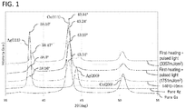
- peak angles are determined from an X-ray diffraction profile and alloying is assessed on the basis of the difference(s) from the peak angle(s) of pure copper and/or pure silver.
- a peak assigned to copper and a peak assigned to silver are observed, and hence, both a silver phase and a copper phase are present.
- the copper-silver alloy synthesized in the present invention has excellent oxidation resistance and can be inhibited from suffering migration.
- the requirement concerning the difference(s) from the peak angle(s) of pure copper and/or pure silver means that the alloy is a copper-silver alloy consisting of Cu and Ag and satisfying the requirement that the difference between a peak of (111) plane angle of the Cu and a peak of (111) plane angle of pure Cu is at least 0.3% of the peak of (111) plane angle of the pure Cu and/or the requirement that the difference between a peak of (111) plane angle of the Ag and a peak of (111) plane angle of pure Ag is at least 0.1% of the peak of (111) plane angle of the pure Ag.
- the difference between the peak of (111) plane angle of the Cu and the peak of (111) plane angle of pure Cu is at least 0.3% of the peak of (111) plane angle of the pure Cu and the difference between the peak of (111) plane angle of the Ag and the peak of (111) plane angle of pure Ag is at least 0.1% of the peak of (111) plane angle of the pure Ag.
- this alloy has more excellent oxidation resistance and is more inhibited from suffering migration.
- a conduction part can be formed on a substrate.
- the term "conduction part" in the present invention means, for example, a wiring, a connecting part which connects a wiring to a terminal, or the like.
- that term means any of all the conductive portions of a wearable device.
- the conduction part obtained in the present invention includes a copper phase and a silver phase and, despite this, the two phases are in a finely and evenly dispersed state.
- the conduction part shows excellent oxidation resistance and low resistivity.
- the copper-silver inks shown in Table 1 were each printed on a polyimide film (thickness: 25 ⁇ m) (manufactured by Du Pont-Toray Co., Ltd.; Type No. Kapton 100N) by screen printing so as to form a square pattern of 2 cm ⁇ 2 cm.
- this substrate was preheated in the same atmosphere as in first-heating in a heating oven under the conditions shown in Table 1.
- the glass substrate which had undergone the preheating was subjected, in the state of being held in the heating oven used in the preheating, to first-heating under the conditions shown in Table 1.
- a Cu:Ag mass ratio after the heating was calculated from the copper salt content and silver salt content in the copper-silver ink.
- the glass substrate was taken out of the heating oven and cooled to room temperature.
- the glass substrate which had been cooled was irradiated in the air with the pulse wave 1, pulse wave 2, or pulse wave 3 shown below, using Pulse Forge 3300, manufactured by Novacentrix.
- the electroconductive patterns thus formed each had a thickness of 25 ⁇ m.
- the synthesized patterns were each examined by XRD (X-ray diffractometry: curved IP X-ray diffractometer RINT RAPID II, manufactured by Rigaku Corp.; measurement conditions: continuous scanning with standard holder; X-ray tube, Cu (40 kV/30 mA); collimator, f 0.8 mm; ⁇ , 20°; f, 1/sec; scanning time, 360 sec; receiving slit (RS), 0.15 mm).
- XRD X-ray diffractometry: curved IP X-ray diffractometer RINT RAPID II, manufactured by Rigaku Corp.
- measurement conditions continuous scanning with standard holder; X-ray tube, Cu (40 kV/30 mA); collimator, f 0.8 mm; ⁇ , 20°; f, 1/sec; scanning time, 360 sec; receiving slit (RS), 0.15 mm).
- RS receiving slit
- Resistivity was measured by the four-point method using measuring device Iozesta-GP MCP-T610, manufactured by Mitsubishi Chemical Corp.
- the four-point probe used in the measurement was ESP probe (MCP-TP08P, No. 014052B).
- Comparative Example 1 and Comparative Example 2 a raw material for synthesizing a copper-silver alloy was not incorporated.
- Comparative Examples 3 to 10 a copper-silver alloy was not obtained because the second-heating was omitted.
- Comparative Examples 3 and 4 among these an electroconductive pattern was not formed because the heating temperature in the first-heating was low and the organic components were not decomposed, and the resistivity measurement was impossible.
- Comparative Examples 5 to 7, 9, and 10 gave electroconductive patterns in which the crystal nuclei were in the state of being in mere physical contact with one another and which showed high resistivity, because the second-heating was omitted although the heating temperature in the first-heating was high and the organic components were sufficiently decomposed.
- Comparative Example 8 the first-heating only was performed in the air, and an electroconductive pattern was hence not formed due to the oxidation of the copper. The resistivity measurement was impossible.
- FIG. 1 is a chart showing the results of an X-ray diffractometry (XRD) experiment obtained in Comparative Example 1, Comparative Example 2, Comparative Example 6, Invention Example 13, and Invention Example 9.
- XRD X-ray diffractometry
- Comparative Example 6 the peak angles for the Ag (111) plane and Cu (111) plane were respectively the same as those for pure Ag and pure Cu, showing that the silver and the copper had not been alloyed. This is because the second-heating was omitted in Comparative Example 6.
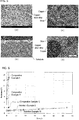
- FIG. 2 shows surface SEM photographs of the conduction parts obtained in Comparative Example 6, Invention Example 13, and Invention Example 9.
- FIG. 2(a) is a surface SEM photograph in the case of Comparative Example 6
- FIG. 2(b) is a surface SEM photograph in the case of Invention Example 13
- FIG. 2(c) is a surface SEM photograph in the case of Invention Example 9.
- the average grain diameter of crystal nuclei was determined by taking ten photographs of different portions of a sample, extracting a hundred crystal nucleus grain diameters from each photograph, subjecting the 1,000 grain diameters in total to image analysis to calculate the projected-area equivalent circular diameter of each grain, and calculating the arithmetic mean of these diameter values.
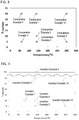
- FIG. 3 is a chart showing the results of alloying in Comparative Example 3 to Comparative Example 7, Comparative Example 9, and Comparative Example 10.
- FIG. 4 is a chart showing the results of alloying in Invention Example 1, Invention Examples 3 to 5, Invention Example 9, Invention Example 14, and Invention Example 15.
- a copper-silver alloy was not obtained in the Comparative Examples regardless of the heating temperature or heating time in the first-heating. It was thus found that the mere formation of crystal nuclei did not result in alloy formation.
- copper-silver alloys were obtained in the Invention Examples regardless of the heating conditions for the first-heating, because the coating copper-silver inks had undergone both the first-heating and the second-heating.
- FIG. 5 shows surface SEM photographs and rupture-surface SEM photographs obtained in Invention Example 9, and Comparative Reference Example in which metallic silver was melted at 1,200°C in an inert atmosphere, metallic copper was thereafter introduced, and the silver and the copper were then mixed for 30 minutes and alloyed.
- FIG. 5(a) is a surface SEM photograph in Invention Example 9;
- FIG. 5(b) is a rupture-surface SEM photograph in Invention Example 9;
- FIG. 5(c) is a surface SEM photograph in Comparative Reference Example;
- FIG. 5(a) is a surface SEM photograph in Comparative Reference Example.
- FIG. 6 is a chart showing relationships between holding time and resistance which were obtained for the samples of Invention Example 9, Invention Example 10, Comparative Example 1, Comparative Example 5, and Comparative Example 11, held in the air at 180°C.
- the samples of Invention Examples 9 and 10 were less apt to oxidize and were inhibited from increasing in resistance, because these samples were copper-silver alloys. Meanwhile, the samples of the Comparative Examples were each found not to have oxidation resistance.
- the synthesis method of the present invention can easily form a conduction part having excellent oxidation resistance, at a low temperature in a short time period, as compared with conventional methods.
- the present invention can hence be applied to devices for which formation of fine wiring is necessary, such as, in particular, wearable devices.
Landscapes
- Chemical & Material Sciences (AREA)
- Engineering & Computer Science (AREA)
- Materials Engineering (AREA)
- Organic Chemistry (AREA)
- Mechanical Engineering (AREA)
- Metallurgy (AREA)
- Chemical Kinetics & Catalysis (AREA)
- General Chemical & Material Sciences (AREA)
- Wood Science & Technology (AREA)
- Life Sciences & Earth Sciences (AREA)
- Manufacturing & Machinery (AREA)
- Physics & Mathematics (AREA)
- Microelectronics & Electronic Packaging (AREA)
- Health & Medical Sciences (AREA)
- Toxicology (AREA)
- Thermal Sciences (AREA)
- Dispersion Chemistry (AREA)
- Spectroscopy & Molecular Physics (AREA)
- Powder Metallurgy (AREA)
- Inks, Pencil-Leads, Or Crayons (AREA)
- Conductive Materials (AREA)
- Other Surface Treatments For Metallic Materials (AREA)
- Non-Insulated Conductors (AREA)
- Manufacturing Of Electric Cables (AREA)
- Parts Printed On Printed Circuit Boards (AREA)
Applications Claiming Priority (2)
| Application Number | Priority Date | Filing Date | Title |
|---|---|---|---|
| JP2017144038 | 2017-07-25 | ||
| PCT/JP2018/027602 WO2019022039A1 (ja) | 2017-07-25 | 2018-07-24 | 銅銀合金の合成方法、導通部の形成方法、銅銀合金、および導通部 |
Publications (2)
| Publication Number | Publication Date |
|---|---|
| EP3660185A1 true EP3660185A1 (de) | 2020-06-03 |
| EP3660185A4 EP3660185A4 (de) | 2020-08-05 |
Family
ID=65041423
Family Applications (1)
| Application Number | Title | Priority Date | Filing Date |
|---|---|---|---|
| EP18838388.9A Pending EP3660185A4 (de) | 2017-07-25 | 2018-07-24 | Verfahren zur synthetisierung einer kupfer-silber-legierung, verfahren zur formung eines leitungsteils, kupfer-silber-legierung und leitungsteil |
Country Status (8)
| Country | Link |
|---|---|
| US (2) | US11217359B2 (de) |
| EP (1) | EP3660185A4 (de) |
| JP (1) | JP6499385B1 (de) |
| KR (1) | KR102163511B1 (de) |
| CN (2) | CN111032912B (de) |
| PH (1) | PH12020500186B1 (de) |
| TW (1) | TWI668709B (de) |
| WO (1) | WO2019022039A1 (de) |
Family Cites Families (19)
| Publication number | Priority date | Publication date | Assignee | Title |
|---|---|---|---|---|
| US20030148024A1 (en) | 2001-10-05 | 2003-08-07 | Kodas Toivo T. | Low viscosity precursor compositons and methods for the depositon of conductive electronic features |
| JP4583164B2 (ja) * | 2004-12-28 | 2010-11-17 | 三井金属鉱業株式会社 | 銀銅複合粉及び銀銅複合粉の製造方法 |
| US8506849B2 (en) * | 2008-03-05 | 2013-08-13 | Applied Nanotech Holdings, Inc. | Additives and modifiers for solvent- and water-based metallic conductive inks |
| CN102675960B (zh) | 2011-03-08 | 2015-08-05 | 深圳市尊业纳米材料有限公司 | 一种纳米铜锡合金导电油墨及其制备方法和使用方法 |
| CN102270514A (zh) * | 2011-05-03 | 2011-12-07 | 华中科技大学 | 一种均相导电浆料 |
| KR101275856B1 (ko) * | 2011-06-21 | 2013-06-18 | 한국과학기술연구원 | 금속 산화물 패턴의 형성 방법 및 이를 이용한 박막 트랜지스터 제조 방법 |
| CN103890960A (zh) * | 2011-07-25 | 2014-06-25 | 日立化成株式会社 | 元件及太阳能电池 |
| CN103945959B (zh) | 2011-11-16 | 2016-10-12 | M技术株式会社 | 固体金属合金 |
| WO2013073068A1 (ja) | 2011-11-16 | 2013-05-23 | エム・テクニック株式会社 | 銀銅合金粒子の製造方法 |
| EP2826575B1 (de) | 2012-03-16 | 2024-08-07 | M Technique Co., Ltd. | Herstellungsverfahren von nanopartikeln aus fester gold-nickel-legierung |
| JP5991830B2 (ja) | 2012-03-19 | 2016-09-14 | 国立大学法人大阪大学 | 導電パターン形成方法及び光照射またはマイクロ波加熱による導電パターン形成用組成物 |
| CN102867595B (zh) * | 2012-09-26 | 2015-12-09 | 江阴市电工合金有限公司 | 高耐磨铜银合金接触线及其生产方法 |
| WO2014156489A1 (ja) * | 2013-03-26 | 2014-10-02 | 株式会社カネカ | 導電性フィルム基板、透明導電性フィルムおよびその製造方法、ならびにタッチパネル |
| CN103320642B (zh) * | 2013-06-15 | 2015-04-08 | 山东亨圆铜业有限公司 | 铁路电气化用铜银合金接触导线的制备方法 |
| CN104407735B (zh) | 2014-11-11 | 2018-05-22 | 长沙市宇顺显示技术有限公司 | 触摸屏引线导电线路及其制作方法和触屏手机 |
| JP5983805B2 (ja) | 2015-03-06 | 2016-09-06 | 東ソー株式会社 | 導電性インク組成物、電気的導通部位の製造方法、及びその用途 |
| JP2017041504A (ja) * | 2015-08-18 | 2017-02-23 | 国立研究開発法人産業技術総合研究所 | フレキシブル抵抗器及びその製造方法、並びに印刷配線装置 |
| JP2017074702A (ja) * | 2015-10-14 | 2017-04-20 | 凸版印刷株式会社 | 印刷版、印刷版の製造方法、印刷物、および印刷物の製造方法 |
| CN105921737B (zh) | 2016-04-28 | 2018-01-19 | 中南大学 | 一种铜银复合粉的制备方法和导电胶 |
-
2018
- 2018-07-23 TW TW107125313A patent/TWI668709B/zh active
- 2018-07-24 PH PH1/2020/500186A patent/PH12020500186B1/en unknown
- 2018-07-24 JP JP2018565905A patent/JP6499385B1/ja active Active
- 2018-07-24 CN CN201880049672.8A patent/CN111032912B/zh active Active
- 2018-07-24 WO PCT/JP2018/027602 patent/WO2019022039A1/ja not_active Ceased
- 2018-07-24 EP EP18838388.9A patent/EP3660185A4/de active Pending
- 2018-07-24 KR KR1020207005102A patent/KR102163511B1/ko active Active
- 2018-07-24 CN CN202011191614.4A patent/CN112301346B/zh active Active
- 2018-07-24 US US16/634,002 patent/US11217359B2/en active Active
-
2021
- 2021-08-09 US US17/397,500 patent/US12119131B2/en active Active
Also Published As
| Publication number | Publication date |
|---|---|
| US20200381136A1 (en) | 2020-12-03 |
| KR102163511B1 (ko) | 2020-10-08 |
| JPWO2019022039A1 (ja) | 2019-07-25 |
| US20210366627A1 (en) | 2021-11-25 |
| CN112301346A (zh) | 2021-02-02 |
| TW201909198A (zh) | 2019-03-01 |
| CN111032912A (zh) | 2020-04-17 |
| EP3660185A4 (de) | 2020-08-05 |
| WO2019022039A1 (ja) | 2019-01-31 |
| PH12020500186B1 (en) | 2023-07-26 |
| PH12020500186A1 (en) | 2020-09-14 |
| JP6499385B1 (ja) | 2019-04-10 |
| US11217359B2 (en) | 2022-01-04 |
| TWI668709B (zh) | 2019-08-11 |
| US12119131B2 (en) | 2024-10-15 |
| CN111032912B (zh) | 2021-03-09 |
| KR20200024331A (ko) | 2020-03-06 |
| CN112301346B (zh) | 2023-02-28 |
Similar Documents
| Publication | Publication Date | Title |
|---|---|---|
| JPWO2009078448A1 (ja) | 銅導体膜及びその製造方法、導電性基板及びその製造方法、銅導体配線及びその製造方法、並びに処理液 | |
| JP2005240088A (ja) | 銅微粒子とその製造方法及び銅微粒子分散液 | |
| KR20140125366A (ko) | 은 미립자와 그의 제조법, 및 상기 은 미립자를 함유하는 도전성 페이스트, 도전성 막 및 전자 디바이스 | |
| JP7139590B2 (ja) | 導体形成用組成物、並びに接合体及びその製造方法 | |
| Joo et al. | Laser sintering of Cu paste film printed on polyimide substrate | |
| TW201637994A (zh) | 銀微粒子組成物 | |
| JP2007321215A (ja) | 金属ナノ粒子分散体および金属被膜 | |
| KR102260398B1 (ko) | 금속 나노 미립자의 제조 방법 | |
| JP2015049973A (ja) | 導電性ペースト及びそれに用いる複合ニッケル微粒子の製造方法 | |
| CN114829042A (zh) | 银膏及其制造方法以及接合体的制造方法 | |
| JP6814529B2 (ja) | 銀粉およびその製造方法 | |
| JP2014029845A (ja) | 導電性ペーストの製造方法 | |
| US12119131B2 (en) | Method for synthesizing copper-silver alloy, method for forming conduction part, copper-silver alloy, and conduction part | |
| KR20110059714A (ko) | 복합나노입자 및 그 제조방법 | |
| JP6118193B2 (ja) | 分散性ニッケル微粒子スラリーの製造方法 | |
| JP2021071440A (ja) | 機能性ペースト用機能性粉末の評価方法及び機能性ペースト用機能性粉末の製造方法 | |
| JP2007197755A (ja) | 金属ナノ粒子の製造方法、金属ナノ粒子、導電性組成物および電子デバイス | |
| JP5286846B2 (ja) | 導電性基板及びその製造方法、並びに銅配線基板及びその製造方法 | |
| JP2016145397A (ja) | 銅膜の製造方法及びそれにより得られた導電体 | |
| JP4624743B2 (ja) | 銀薄膜の製造方法及び銅−銀合金薄膜の製造方法 | |
| JP7199285B2 (ja) | 銀パラジウム合金粉末およびその利用 | |
| JPWO2016139967A1 (ja) | ニッケル粒子、その製造方法及び導電性ペースト | |
| WO2017179524A1 (ja) | 銀被覆銅粉およびその製造方法 | |
| JP5170989B2 (ja) | 導電性銅被膜の製造方法 | |
| JP2003328001A (ja) | 金属粉末およびその製造方法 |
Legal Events
| Date | Code | Title | Description |
|---|---|---|---|
| STAA | Information on the status of an ep patent application or granted ep patent |
Free format text: STATUS: THE INTERNATIONAL PUBLICATION HAS BEEN MADE |
|
| PUAI | Public reference made under article 153(3) epc to a published international application that has entered the european phase |
Free format text: ORIGINAL CODE: 0009012 |
|
| STAA | Information on the status of an ep patent application or granted ep patent |
Free format text: STATUS: REQUEST FOR EXAMINATION WAS MADE |
|
| 17P | Request for examination filed |
Effective date: 20200220 |
|
| AK | Designated contracting states |
Kind code of ref document: A1 Designated state(s): AL AT BE BG CH CY CZ DE DK EE ES FI FR GB GR HR HU IE IS IT LI LT LU LV MC MK MT NL NO PL PT RO RS SE SI SK SM TR |
|
| AX | Request for extension of the european patent |
Extension state: BA ME |
|
| A4 | Supplementary search report drawn up and despatched |
Effective date: 20200702 |
|
| RIC1 | Information provided on ipc code assigned before grant |
Ipc: H05K 3/12 20060101ALI20200626BHEP Ipc: C09D 11/037 20140101ALI20200626BHEP Ipc: C22C 9/00 20060101ALI20200626BHEP Ipc: C23C 18/08 20060101ALI20200626BHEP Ipc: C09D 11/52 20140101ALI20200626BHEP Ipc: C23C 26/00 20060101AFI20200626BHEP Ipc: C23C 18/14 20060101ALI20200626BHEP Ipc: C22C 5/08 20060101ALI20200626BHEP Ipc: H01B 13/00 20060101ALI20200626BHEP |
|
| DAV | Request for validation of the european patent (deleted) | ||
| DAX | Request for extension of the european patent (deleted) | ||
| STAA | Information on the status of an ep patent application or granted ep patent |
Free format text: STATUS: EXAMINATION IS IN PROGRESS |
|
| 17Q | First examination report despatched |
Effective date: 20230612 |