EP3617773B1 - Anzeigevorrichtung - Google Patents
Anzeigevorrichtung Download PDFInfo
- Publication number
- EP3617773B1 EP3617773B1 EP19186981.7A EP19186981A EP3617773B1 EP 3617773 B1 EP3617773 B1 EP 3617773B1 EP 19186981 A EP19186981 A EP 19186981A EP 3617773 B1 EP3617773 B1 EP 3617773B1
- Authority
- EP
- European Patent Office
- Prior art keywords
- light
- display device
- dimmer
- guide plate
- image
- Prior art date
- Legal status (The legal status is an assumption and is not a legal conclusion. Google has not performed a legal analysis and makes no representation as to the accuracy of the status listed.)
- Active
Links
- 230000003287 optical effect Effects 0.000 claims description 217
- 230000008859 change Effects 0.000 claims description 177
- 230000000644 propagated effect Effects 0.000 claims description 26
- 238000002834 transmittance Methods 0.000 description 130
- 239000000463 material Substances 0.000 description 76
- 238000005286 illumination Methods 0.000 description 68
- 239000000758 substrate Substances 0.000 description 67
- 238000010586 diagram Methods 0.000 description 62
- 239000010410 layer Substances 0.000 description 58
- 238000005259 measurement Methods 0.000 description 48
- 230000002349 favourable effect Effects 0.000 description 42
- 238000000034 method Methods 0.000 description 37
- 239000004973 liquid crystal related substance Substances 0.000 description 36
- 230000004048 modification Effects 0.000 description 34
- 238000012986 modification Methods 0.000 description 34
- 210000001747 pupil Anatomy 0.000 description 24
- 230000005540 biological transmission Effects 0.000 description 22
- 239000003086 colorant Substances 0.000 description 16
- 229920003023 plastic Polymers 0.000 description 15
- 239000011521 glass Substances 0.000 description 14
- 238000009434 installation Methods 0.000 description 14
- 239000000853 adhesive Substances 0.000 description 13
- 230000001070 adhesive effect Effects 0.000 description 13
- 238000004364 calculation method Methods 0.000 description 12
- 230000015654 memory Effects 0.000 description 12
- 239000004033 plastic Substances 0.000 description 12
- 230000003247 decreasing effect Effects 0.000 description 10
- 230000000295 complement effect Effects 0.000 description 9
- 229920005989 resin Polymers 0.000 description 9
- 239000011347 resin Substances 0.000 description 9
- -1 silver halide Chemical class 0.000 description 9
- 238000013461 design Methods 0.000 description 8
- 238000005401 electroluminescence Methods 0.000 description 7
- WEVYAHXRMPXWCK-UHFFFAOYSA-N Acetonitrile Chemical compound CC#N WEVYAHXRMPXWCK-UHFFFAOYSA-N 0.000 description 6
- OKKJLVBELUTLKV-UHFFFAOYSA-N Methanol Chemical compound OC OKKJLVBELUTLKV-UHFFFAOYSA-N 0.000 description 6
- 238000003384 imaging method Methods 0.000 description 6
- 238000007789 sealing Methods 0.000 description 6
- XOLBLPGZBRYERU-UHFFFAOYSA-N tin dioxide Chemical compound O=[Sn]=O XOLBLPGZBRYERU-UHFFFAOYSA-N 0.000 description 6
- 238000005516 engineering process Methods 0.000 description 5
- 230000006870 function Effects 0.000 description 5
- 238000005240 physical vapour deposition Methods 0.000 description 5
- 238000006479 redox reaction Methods 0.000 description 5
- 238000003860 storage Methods 0.000 description 5
- 230000002123 temporal effect Effects 0.000 description 5
- IAZDPXIOMUYVGZ-UHFFFAOYSA-N Dimethylsulphoxide Chemical compound CS(C)=O IAZDPXIOMUYVGZ-UHFFFAOYSA-N 0.000 description 4
- 230000001133 acceleration Effects 0.000 description 4
- 238000005229 chemical vapour deposition Methods 0.000 description 4
- 230000004907 flux Effects 0.000 description 4
- 210000003128 head Anatomy 0.000 description 4
- 239000011159 matrix material Substances 0.000 description 4
- 239000002609 medium Substances 0.000 description 4
- 229910052751 metal Inorganic materials 0.000 description 4
- 239000002184 metal Substances 0.000 description 4
- 239000002985 plastic film Substances 0.000 description 4
- 239000000565 sealant Substances 0.000 description 4
- 239000007787 solid Substances 0.000 description 4
- 239000000126 substance Substances 0.000 description 4
- 238000012360 testing method Methods 0.000 description 4
- VYPSYNLAJGMNEJ-UHFFFAOYSA-N Silicium dioxide Chemical compound O=[Si]=O VYPSYNLAJGMNEJ-UHFFFAOYSA-N 0.000 description 3
- 239000000956 alloy Substances 0.000 description 3
- 238000004070 electrodeposition Methods 0.000 description 3
- 238000004519 manufacturing process Methods 0.000 description 3
- 239000002245 particle Substances 0.000 description 3
- 238000007639 printing Methods 0.000 description 3
- 239000004065 semiconductor Substances 0.000 description 3
- 229910052709 silver Inorganic materials 0.000 description 3
- 239000004332 silver Substances 0.000 description 3
- 238000001771 vacuum deposition Methods 0.000 description 3
- 230000000007 visual effect Effects 0.000 description 3
- XLOMVQKBTHCTTD-UHFFFAOYSA-N zinc oxide Inorganic materials [Zn]=O XLOMVQKBTHCTTD-UHFFFAOYSA-N 0.000 description 3
- 239000011787 zinc oxide Substances 0.000 description 3
- 239000004698 Polyethylene Substances 0.000 description 2
- XUIMIQQOPSSXEZ-UHFFFAOYSA-N Silicon Chemical compound [Si] XUIMIQQOPSSXEZ-UHFFFAOYSA-N 0.000 description 2
- PPBRXRYQALVLMV-UHFFFAOYSA-N Styrene Chemical compound C=CC1=CC=CC=C1 PPBRXRYQALVLMV-UHFFFAOYSA-N 0.000 description 2
- ZMZDMBWJUHKJPS-UHFFFAOYSA-M Thiocyanate anion Chemical compound [S-]C#N ZMZDMBWJUHKJPS-UHFFFAOYSA-M 0.000 description 2
- GWEVSGVZZGPLCZ-UHFFFAOYSA-N Titan oxide Chemical compound O=[Ti]=O GWEVSGVZZGPLCZ-UHFFFAOYSA-N 0.000 description 2
- 229910045601 alloy Inorganic materials 0.000 description 2
- 230000003190 augmentative effect Effects 0.000 description 2
- 230000006399 behavior Effects 0.000 description 2
- 229920002678 cellulose Polymers 0.000 description 2
- 238000001723 curing Methods 0.000 description 2
- 238000005520 cutting process Methods 0.000 description 2
- 230000000694 effects Effects 0.000 description 2
- 239000005357 flat glass Substances 0.000 description 2
- 125000005843 halogen group Chemical group 0.000 description 2
- ZMZDMBWJUHKJPS-UHFFFAOYSA-N hydrogen thiocyanate Natural products SC#N ZMZDMBWJUHKJPS-UHFFFAOYSA-N 0.000 description 2
- PJXISJQVUVHSOJ-UHFFFAOYSA-N indium(III) oxide Inorganic materials [O-2].[O-2].[O-2].[In+3].[In+3] PJXISJQVUVHSOJ-UHFFFAOYSA-N 0.000 description 2
- AMGQUBHHOARCQH-UHFFFAOYSA-N indium;oxotin Chemical compound [In].[Sn]=O AMGQUBHHOARCQH-UHFFFAOYSA-N 0.000 description 2
- VRIVJOXICYMTAG-IYEMJOQQSA-L iron(ii) gluconate Chemical compound [Fe+2].OC[C@@H](O)[C@@H](O)[C@H](O)[C@@H](O)C([O-])=O.OC[C@@H](O)[C@@H](O)[C@H](O)[C@@H](O)C([O-])=O VRIVJOXICYMTAG-IYEMJOQQSA-L 0.000 description 2
- 238000012423 maintenance Methods 0.000 description 2
- 238000012544 monitoring process Methods 0.000 description 2
- 239000005304 optical glass Substances 0.000 description 2
- 239000003960 organic solvent Substances 0.000 description 2
- VVRQVWSVLMGPRN-UHFFFAOYSA-N oxotungsten Chemical class [W]=O VVRQVWSVLMGPRN-UHFFFAOYSA-N 0.000 description 2
- 238000000059 patterning Methods 0.000 description 2
- 229920006255 plastic film Polymers 0.000 description 2
- 229920000573 polyethylene Polymers 0.000 description 2
- 229920006324 polyoxymethylene Polymers 0.000 description 2
- 238000012545 processing Methods 0.000 description 2
- 239000010703 silicon Substances 0.000 description 2
- 229910052710 silicon Inorganic materials 0.000 description 2
- RHUVFRWZKMEWNS-UHFFFAOYSA-M silver thiocyanate Chemical compound [Ag+].[S-]C#N RHUVFRWZKMEWNS-UHFFFAOYSA-M 0.000 description 2
- 239000005361 soda-lime glass Substances 0.000 description 2
- 238000004544 sputter deposition Methods 0.000 description 2
- PBCFLUZVCVVTBY-UHFFFAOYSA-N tantalum pentoxide Inorganic materials O=[Ta](=O)O[Ta](=O)=O PBCFLUZVCVVTBY-UHFFFAOYSA-N 0.000 description 2
- 229910001930 tungsten oxide Inorganic materials 0.000 description 2
- XLYOFNOQVPJJNP-UHFFFAOYSA-N water Substances O XLYOFNOQVPJJNP-UHFFFAOYSA-N 0.000 description 2
- AFABGHUZZDYHJO-UHFFFAOYSA-N 2-Methylpentane Chemical compound CCCC(C)C AFABGHUZZDYHJO-UHFFFAOYSA-N 0.000 description 1
- VEXZGXHMUGYJMC-UHFFFAOYSA-M Chloride anion Chemical compound [Cl-] VEXZGXHMUGYJMC-UHFFFAOYSA-M 0.000 description 1
- JOYRKODLDBILNP-UHFFFAOYSA-N Ethyl urethane Chemical compound CCOC(N)=O JOYRKODLDBILNP-UHFFFAOYSA-N 0.000 description 1
- 239000002033 PVDF binder Substances 0.000 description 1
- 229930040373 Paraformaldehyde Natural products 0.000 description 1
- 229930182556 Polyacetal Natural products 0.000 description 1
- 239000004952 Polyamide Substances 0.000 description 1
- 239000004962 Polyamide-imide Substances 0.000 description 1
- 239000004695 Polyether sulfone Substances 0.000 description 1
- 239000004642 Polyimide Substances 0.000 description 1
- 239000004721 Polyphenylene oxide Substances 0.000 description 1
- 239000004734 Polyphenylene sulfide Substances 0.000 description 1
- 239000004743 Polypropylene Substances 0.000 description 1
- 239000004793 Polystyrene Substances 0.000 description 1
- BQCADISMDOOEFD-UHFFFAOYSA-N Silver Chemical compound [Ag] BQCADISMDOOEFD-UHFFFAOYSA-N 0.000 description 1
- XTXRWKRVRITETP-UHFFFAOYSA-N Vinyl acetate Chemical compound CC(=O)OC=C XTXRWKRVRITETP-UHFFFAOYSA-N 0.000 description 1
- NIXOWILDQLNWCW-UHFFFAOYSA-N acrylic acid group Chemical group C(C=C)(=O)O NIXOWILDQLNWCW-UHFFFAOYSA-N 0.000 description 1
- 230000004075 alteration Effects 0.000 description 1
- 229910052782 aluminium Inorganic materials 0.000 description 1
- XAGFODPZIPBFFR-UHFFFAOYSA-N aluminium Chemical compound [Al] XAGFODPZIPBFFR-UHFFFAOYSA-N 0.000 description 1
- 238000003491 array Methods 0.000 description 1
- 230000004888 barrier function Effects 0.000 description 1
- 238000005452 bending Methods 0.000 description 1
- 230000008901 benefit Effects 0.000 description 1
- 239000001913 cellulose Substances 0.000 description 1
- 229920002301 cellulose acetate Polymers 0.000 description 1
- 239000003795 chemical substances by application Substances 0.000 description 1
- 238000000576 coating method Methods 0.000 description 1
- 229910052681 coesite Inorganic materials 0.000 description 1
- 229920001940 conductive polymer Polymers 0.000 description 1
- 229920001577 copolymer Polymers 0.000 description 1
- 229910052906 cristobalite Inorganic materials 0.000 description 1
- 210000002858 crystal cell Anatomy 0.000 description 1
- 230000007850 degeneration Effects 0.000 description 1
- 239000006185 dispersion Substances 0.000 description 1
- 239000002612 dispersion medium Substances 0.000 description 1
- 238000010494 dissociation reaction Methods 0.000 description 1
- 230000005593 dissociations Effects 0.000 description 1
- 210000003027 ear inner Anatomy 0.000 description 1
- 230000007613 environmental effect Effects 0.000 description 1
- 239000003822 epoxy resin Substances 0.000 description 1
- 238000005530 etching Methods 0.000 description 1
- 239000004811 fluoropolymer Substances 0.000 description 1
- 229920002313 fluoropolymer Polymers 0.000 description 1
- 239000011888 foil Substances 0.000 description 1
- 238000009499 grossing Methods 0.000 description 1
- 150000003949 imides Chemical class 0.000 description 1
- 229910010272 inorganic material Inorganic materials 0.000 description 1
- 239000011147 inorganic material Substances 0.000 description 1
- 239000007788 liquid Substances 0.000 description 1
- 239000007769 metal material Substances 0.000 description 1
- VLKZOEOYAKHREP-UHFFFAOYSA-N methyl pentane Natural products CCCCCC VLKZOEOYAKHREP-UHFFFAOYSA-N 0.000 description 1
- 239000000203 mixture Substances 0.000 description 1
- 238000013008 moisture curing Methods 0.000 description 1
- 239000011368 organic material Substances 0.000 description 1
- 125000000951 phenoxy group Chemical group [H]C1=C([H])C([H])=C(O*)C([H])=C1[H] 0.000 description 1
- 238000000016 photochemical curing Methods 0.000 description 1
- 238000005498 polishing Methods 0.000 description 1
- 229920003207 poly(ethylene-2,6-naphthalate) Polymers 0.000 description 1
- 229920003229 poly(methyl methacrylate) Polymers 0.000 description 1
- 229920002492 poly(sulfone) Polymers 0.000 description 1
- 229920002647 polyamide Polymers 0.000 description 1
- 229920002312 polyamide-imide Polymers 0.000 description 1
- 239000004417 polycarbonate Substances 0.000 description 1
- 229920000515 polycarbonate Polymers 0.000 description 1
- 229920005668 polycarbonate resin Polymers 0.000 description 1
- 239000004431 polycarbonate resin Substances 0.000 description 1
- 229920000647 polyepoxide Polymers 0.000 description 1
- 229920000570 polyether Polymers 0.000 description 1
- 229920006393 polyether sulfone Polymers 0.000 description 1
- 239000011112 polyethylene naphthalate Substances 0.000 description 1
- 229920000139 polyethylene terephthalate Polymers 0.000 description 1
- 239000005020 polyethylene terephthalate Substances 0.000 description 1
- 229920001721 polyimide Polymers 0.000 description 1
- 229920000642 polymer Polymers 0.000 description 1
- 239000002952 polymeric resin Substances 0.000 description 1
- 239000004926 polymethyl methacrylate Substances 0.000 description 1
- 229920000098 polyolefin Polymers 0.000 description 1
- 229920000069 polyphenylene sulfide Polymers 0.000 description 1
- 229920001155 polypropylene Polymers 0.000 description 1
- 229920005673 polypropylene based resin Polymers 0.000 description 1
- 229920002223 polystyrene Polymers 0.000 description 1
- 229920001343 polytetrafluoroethylene Polymers 0.000 description 1
- 239000004810 polytetrafluoroethylene Substances 0.000 description 1
- 229940058401 polytetrafluoroethylene Drugs 0.000 description 1
- 229920000123 polythiophene Polymers 0.000 description 1
- 229920002981 polyvinylidene fluoride Polymers 0.000 description 1
- 230000004044 response Effects 0.000 description 1
- 230000002441 reversible effect Effects 0.000 description 1
- 238000004904 shortening Methods 0.000 description 1
- 239000000377 silicon dioxide Substances 0.000 description 1
- 239000002356 single layer Substances 0.000 description 1
- 239000011029 spinel Substances 0.000 description 1
- 229910052596 spinel Inorganic materials 0.000 description 1
- 230000000638 stimulation Effects 0.000 description 1
- 229910052682 stishovite Inorganic materials 0.000 description 1
- 230000001360 synchronised effect Effects 0.000 description 1
- 229920003002 synthetic resin Polymers 0.000 description 1
- 229920001187 thermosetting polymer Polymers 0.000 description 1
- 229910052905 tridymite Inorganic materials 0.000 description 1
- 238000009736 wetting Methods 0.000 description 1
- YVTHLONGBIQYBO-UHFFFAOYSA-N zinc indium(3+) oxygen(2-) Chemical compound [O--].[Zn++].[In+3] YVTHLONGBIQYBO-UHFFFAOYSA-N 0.000 description 1
Images


Classifications
-
- G—PHYSICS
- G02—OPTICS
- G02B—OPTICAL ELEMENTS, SYSTEMS OR APPARATUS
- G02B27/00—Optical systems or apparatus not provided for by any of the groups G02B1/00 - G02B26/00, G02B30/00
- G02B27/01—Head-up displays
- G02B27/017—Head mounted
- G02B27/0172—Head mounted characterised by optical features
-
- G—PHYSICS
- G02—OPTICS
- G02B—OPTICAL ELEMENTS, SYSTEMS OR APPARATUS
- G02B27/00—Optical systems or apparatus not provided for by any of the groups G02B1/00 - G02B26/00, G02B30/00
- G02B27/01—Head-up displays
- G02B27/017—Head mounted
-
- G—PHYSICS
- G02—OPTICS
- G02B—OPTICAL ELEMENTS, SYSTEMS OR APPARATUS
- G02B27/00—Optical systems or apparatus not provided for by any of the groups G02B1/00 - G02B26/00, G02B30/00
- G02B27/01—Head-up displays
- G02B27/0101—Head-up displays characterised by optical features
-
- G—PHYSICS
- G02—OPTICS
- G02F—OPTICAL DEVICES OR ARRANGEMENTS FOR THE CONTROL OF LIGHT BY MODIFICATION OF THE OPTICAL PROPERTIES OF THE MEDIA OF THE ELEMENTS INVOLVED THEREIN; NON-LINEAR OPTICS; FREQUENCY-CHANGING OF LIGHT; OPTICAL LOGIC ELEMENTS; OPTICAL ANALOGUE/DIGITAL CONVERTERS
- G02F1/00—Devices or arrangements for the control of the intensity, colour, phase, polarisation or direction of light arriving from an independent light source, e.g. switching, gating or modulating; Non-linear optics
- G02F1/01—Devices or arrangements for the control of the intensity, colour, phase, polarisation or direction of light arriving from an independent light source, e.g. switching, gating or modulating; Non-linear optics for the control of the intensity, phase, polarisation or colour
- G02F1/0121—Operation of devices; Circuit arrangements, not otherwise provided for in this subclass
-
- G—PHYSICS
- G02—OPTICS
- G02F—OPTICAL DEVICES OR ARRANGEMENTS FOR THE CONTROL OF LIGHT BY MODIFICATION OF THE OPTICAL PROPERTIES OF THE MEDIA OF THE ELEMENTS INVOLVED THEREIN; NON-LINEAR OPTICS; FREQUENCY-CHANGING OF LIGHT; OPTICAL LOGIC ELEMENTS; OPTICAL ANALOGUE/DIGITAL CONVERTERS
- G02F1/00—Devices or arrangements for the control of the intensity, colour, phase, polarisation or direction of light arriving from an independent light source, e.g. switching, gating or modulating; Non-linear optics
- G02F1/01—Devices or arrangements for the control of the intensity, colour, phase, polarisation or direction of light arriving from an independent light source, e.g. switching, gating or modulating; Non-linear optics for the control of the intensity, phase, polarisation or colour
- G02F1/13—Devices or arrangements for the control of the intensity, colour, phase, polarisation or direction of light arriving from an independent light source, e.g. switching, gating or modulating; Non-linear optics for the control of the intensity, phase, polarisation or colour based on liquid crystals, e.g. single liquid crystal display cells
- G02F1/133—Constructional arrangements; Operation of liquid crystal cells; Circuit arrangements
- G02F1/13306—Circuit arrangements or driving methods for the control of single liquid crystal cells
- G02F1/13318—Circuits comprising a photodetector
-
- G—PHYSICS
- G02—OPTICS
- G02F—OPTICAL DEVICES OR ARRANGEMENTS FOR THE CONTROL OF LIGHT BY MODIFICATION OF THE OPTICAL PROPERTIES OF THE MEDIA OF THE ELEMENTS INVOLVED THEREIN; NON-LINEAR OPTICS; FREQUENCY-CHANGING OF LIGHT; OPTICAL LOGIC ELEMENTS; OPTICAL ANALOGUE/DIGITAL CONVERTERS
- G02F1/00—Devices or arrangements for the control of the intensity, colour, phase, polarisation or direction of light arriving from an independent light source, e.g. switching, gating or modulating; Non-linear optics
- G02F1/01—Devices or arrangements for the control of the intensity, colour, phase, polarisation or direction of light arriving from an independent light source, e.g. switching, gating or modulating; Non-linear optics for the control of the intensity, phase, polarisation or colour
- G02F1/15—Devices or arrangements for the control of the intensity, colour, phase, polarisation or direction of light arriving from an independent light source, e.g. switching, gating or modulating; Non-linear optics for the control of the intensity, phase, polarisation or colour based on an electrochromic effect
- G02F1/163—Operation of electrochromic cells, e.g. electrodeposition cells; Circuit arrangements therefor
-
- G—PHYSICS
- G02—OPTICS
- G02B—OPTICAL ELEMENTS, SYSTEMS OR APPARATUS
- G02B27/00—Optical systems or apparatus not provided for by any of the groups G02B1/00 - G02B26/00, G02B30/00
- G02B27/01—Head-up displays
- G02B27/0101—Head-up displays characterised by optical features
- G02B2027/0118—Head-up displays characterised by optical features comprising devices for improving the contrast of the display / brillance control visibility
-
- G—PHYSICS
- G02—OPTICS
- G02B—OPTICAL ELEMENTS, SYSTEMS OR APPARATUS
- G02B27/00—Optical systems or apparatus not provided for by any of the groups G02B1/00 - G02B26/00, G02B30/00
- G02B27/01—Head-up displays
- G02B27/0101—Head-up displays characterised by optical features
- G02B2027/0132—Head-up displays characterised by optical features comprising binocular systems
-
- G—PHYSICS
- G02—OPTICS
- G02B—OPTICAL ELEMENTS, SYSTEMS OR APPARATUS
- G02B27/00—Optical systems or apparatus not provided for by any of the groups G02B1/00 - G02B26/00, G02B30/00
- G02B27/01—Head-up displays
- G02B27/0101—Head-up displays characterised by optical features
- G02B2027/014—Head-up displays characterised by optical features comprising information/image processing systems
-
- G—PHYSICS
- G02—OPTICS
- G02B—OPTICAL ELEMENTS, SYSTEMS OR APPARATUS
- G02B27/00—Optical systems or apparatus not provided for by any of the groups G02B1/00 - G02B26/00, G02B30/00
- G02B27/01—Head-up displays
- G02B27/017—Head mounted
- G02B2027/0178—Eyeglass type
Definitions
- the present disclosure relates to a display device and more particularly, to a display device using a head-mounted display (HMD).
- HMD head-mounted display
- an augmented reality technology has drawn attention, which combines virtual objects or various kinds of information as additional information and as electronic information with a real environment (or a portion thereof), and presents the combined information.
- a head-mounted display has been examined as a device for presenting visual information, for example.
- the head-mounted display is expected to be applied for job support in the reality environment.
- the head-mounted display may be applied for providing of route guidance information and of technical information to the engineer who performs maintenance, for example.
- the head-mounted display is very convenient since the hands are free.
- the user can see the video or the image and an external environment at the same time. Therefore, the user can move smoothly.
- JP 2006-162767 A discloses a virtual image display device (image display device) in which a virtual image optical system changes a two-dimensional image formed by an image forming device into an enlarged virtual image such that the observer can observe the virtual image.
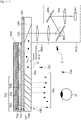
- an image display device 100' includes an image forming device 111 including a plurality of pixels arranged in a two-dimensional matrix, a collimating optical system 112 that converts light emitted from the pixels of the image forming device 111 into parallel light, and an optical device (light guide unit) 120 on which the parallel light converted in the collimating optical system 112 is incident, in which the light is guided, and from which the light is emitted.
- the optical device 120 includes a light guide plate 121 in which incident light propagates while being totally reflected and from which the light is emitted, a first deflection unit 130 (for example, a single-layer light reflecting film) that reflects light incident on the light guide plate 121 so as to be totally reflected in the light guide plate 121, and a second deflection unit 140 (for example, a multi-layer light reflecting film having a multi-layer structure) that allows the light, which has propagated in the light guide plate 121 while being totally reflected, to be emitted from the light guide plate 121.
- a first deflection unit 130 for example, a single-layer light reflecting film
- a second deflection unit 140 for example, a multi-layer light reflecting film having a multi-layer structure
- JP 2007-94175 A discloses a virtual image display device (image display device) using a hologram diffraction grating in which a virtual image optical system changes a two-dimensional image formed by an image forming device into an enlarged virtual image such that the observer can observe the virtual image.
- an image display device 300' basically includes an image forming device 111 that displays an image, a collimating optical system 112, and an optical device (light guide unit) 320, which light displayed on the image forming device 111 is incident on, and which guides the light to a pupil 21 of the observer.
- the optical device 320 includes a light guide plate 321, and first and second diffraction grating members 330 and 340 that are reflective volume hologram diffraction gratings provided on the light guide plate 321.
- each pixel of the image forming device 111 is incident on the collimating optical system 112, and a plurality of parallel light with different incident angles to be incident on the light guide plate 321 is generated by the collimating optical system 112 and is then incident on the light guide plate 321.
- the parallel light is incident on a first surface 322 of the light guide plate 321, and is then emitted therefrom.
- the first diffraction grating member 330 and the second diffraction grating member 340 are attached to a second surface 323 of the light guide plate 321 that is parallel to the first surface 322 of the light guide plate 321.
- the observer can view the displayed image and an external image in an overlapped manner.
- sufficiently high contrast may not be given to the image observed by the observer when the brightness of a surrounding environment in which the image display devices 100' and 300' are located is very high or depending on the content of the displayed image.
- JP 2004-101197 A discloses means for solving the problem.
- a liquid crystal shutter controls the quantity of incident light incident on the pupil of the observer from an outside.
- EP 2535760 A2 discloses a display apparatus including an illumination sensor which measures the intensity of illumination of an environment.
- a control circuit is provided which controls the light transmittance of a dimmer on the basis of a value received from the illumination sensor.
- a first objective of the present disclosure is to provide a display device that provides the observer who wears the display device with a less unpleasant feeling and that does not force the eyes to bear substantial burden even if the quantity of incident light from an outside is changed.
- a second objective of the present disclosure is to provide a display device that does not cause a drop in image display quality due to incident light from an outside, in addition to the first objective of the present disclosure display device.
- a third objective of the present disclosure is to provide a display device having a configuration or a structure that may suppress an increase in overall weight, in addition to the first objective of the present disclosure.
- Some embodiments are directed to a display device comprising a first image display device comprising a light guide plate, a dimmer, and a light control device.
- the light control device is configured to identify a start time of change in quantity of light received by the display device, and control transmissivity of the dimmer based on quantity of light received by the display device, after a predetermined amount of time after the start time has elapsed.
- Some embodiments are directed to a method for use in connection with a display device comprising an image display device and a dimmer, the image display device comprising a light guide plate, the method comprising identifying a start time of change in quantity of light received by the display device, and controlling transmissivity of the dimmer based on quantity of light received by the display device, after a predetermined amount of time after the start time has elapsed.
- Some embodiments are directed to at least one non-transitory computer-readable storage medium storing processor-executable instructions that, when executed by at least one processor, cause the at least one processor to perform a method for use in connection with a display device comprising an image display device and a dimmer, the image display device comprising a light guide plate.
- the method comprises identifying a start time of change in quantity of light received by the display device, and controlling transmissivity of the dimmer based on quantity of light received by the display device, after a predetermined amount of time after the start time has elapsed.
- the light control device calculates a quantity of received light change rate based on a quantity of received light measurement result of the light receiving element, determines a light transmittance change rate in the dimmer based on the quantity of received light change rate, and controls light transmittance of the dimmer based on the determined light transmittance change rate. Therefore, a display device that provides the observer who wears the display device with a less unpleasant feeling and that does not force the eyes to bear substantial burden can be provided even if the quantity of incident light from an outside is changed.
- the light control device determines a start time of a change of a quantity of received light based on a quantity of received light measurement result of the light receiving element, and starts control of light transmittance of the dimmer after elapse of a predetermined time from the start time of the change of the quantity of received light. Therefore, a display device that provides the observer who wears the display device with a less unpleasant feeling and that does not force the eyes to bear substantial burden can be provided even if the quantity of incident light from an outside is changed. Furthermore, the light transmittance of the dimmer is controlled based on the quantity of received light measurement result of the light receiving element. Therefore, the overall structure of the display device can be simplified, and high contrast can be provided to an image observed by the observer. In addition, for example, an observation state of the image can be optimized depending on the illumination of surrounding environment of the display device.
- the dimmer starts a change of light transmittance after elapse of a predetermined time from a start of a change of the quantity of light from an outside. Therefore, a display device that provides the observer who wears the display device with a less unpleasant feeling and that does not force the eyes to bear substantial burden can be provided even if the quantity of incident light from an outside is changed.
- a shielding member that shields incident light to the optical device is arranged in an area of the optical device on which the light emitted from the image forming device is incident.
- the first substrate that forms the dimmer also serves as a component member of the optical device. Therefore, the overall weight of the display device can be decreased, and there is little possibility to provide the user of the display device with an unpleasant feeling.
- the light control device can include a table related to a relationship between the quantity of received light change rate and the light transmittance change rate in the dimmer.
- a table related to a relationship between the quantity of received light change rate and the light transmittance change rate in the dimmer.
- the light control device can further determine a start time of a change of the quantity of received light based on the quantity of received light measurement result of the light receiving element, and can start control of the light transmittance of the dimmer after elapse of a predetermined time from the start time of the change of the quantity of received light.
- the light control device can further include a moving speed calculation unit that calculates a moving speed of the display device, and the light control device can further start control of the light transmittance of the dimmer based on the moving speed of the display device calculated by the moving speed calculation unit.
- the light control device can further include a moving speed calculation unit that calculates a moving speed of the display device, and the light control device can further determine the light transmittance change rate in the dimmer based on the moving speed of the display device calculated by the moving speed calculation unit. Further, in this case, the light control device can further determine a start time of a change of the quantity of received light based on the quantity of received light measurement result of the light receiving element, and the light control device can further start control of the light transmittance of the dimmer based on the moving speed of the display device calculated by the moving speed calculation unit.
- the display device it is favorable to include an area of the optical device on which the light emitted from the image forming device is incident, in a projected image of the shielding member to the optical device.
- the shielding member can be arranged to the optical device way from each other on a side opposite to the image forming device.
- the shielding member may be produced with an opaque plastic material, and such a shielding member can integrally extend from a housing of the image display device, can be installed to the housing of the image display device, can integrally extend from a frame, or can be installed to the frame.
- the shielding member can be arranged on a portion of the optical device on a side opposite to the image forming device, and the shielding member can be arranged in the dimmer.
- the shielding member formed of an opaque material may be, for example, formed on a surface of the optical device based on a physical vapor deposition method (PVD method) or a chemical vapor deposition method (CVD method), may be formed by a printing method, or the like, or may be formed by attaching a film, a sheet, or a foil formed of the opaque material (plastic material, metal material, or alloy material, or the like).
- the display device that includes the above-described various favorable embodiments, it is favorable to include a projected image of an end portion of the dimmer to the optical device, in a projected image of the shielding member to the optical device.
- the second substrate can be thinner than the first substrate.
- the display device further includes
- the light control device can further include a moving speed calculation unit that calculates a moving speed of the display device, and the light control device can further start control of the light transmittance of the dimmer based on the moving speed of the display device calculated by the moving speed calculation unit.
- the quantity of light of the external environment can be measured by the light receiving element.
- the light receiving element measures the quantity of light of an outside area corresponding to a background of an image observed by the observer in the optical device. Further, in the latter case, it is favorable that the light receiving element has directivity to the light to be received.
- Examples of a method of providing the light receiving element with the directivity to the light to be received include a method of arranging a lens on a light incident side of the light receiving element, a method of arranging an aperture on the light incident side of the light receiving element, and a method of providing a slit on the light incident side of the light receiving element and shielding stray light from the side.
- the optical device may include
- the dimmer can be formed of an optical shutter applying a liquid crystal shutter or a color change of a substance generated by an oxidation-reduction reaction of an electrochromic material. That is, the dimmer can be formed of an optical shutter in which a light transmission control material layer is made of a liquid crystal material layer, or an optical shutter in which the light transmission control material layer is made of a substance generated by an oxidation-reduction reaction of an electrochromic material.
- the dimmer is not limited to the above-described examples, and the dimmer can be formed of an optical shutter in which the light transmission control material layer is made of an inorganic electroluminescence material layer, an optical shutter formed of an electrophoretic dispersion liquid in which the light transmission control material layer is made of a number of charged electrophoretic particles and a dispersion medium having a different color from the electrophoretic particles, an optical shutter by an electrodeposition method (electrodeposition) that applies the electrodeposition/dissociation phenomena generated a lossless oxidation-reduction reaction of metal (for example, silver particles), or an optical shutter that controls the light transmittance by an electro-wetting phenomenon.
- an electrodeposition method electrodeposition
- metal for example, silver particles
- the dimmer is an optical shutter in which the light transmission control material layer is made of a liquid crystal material layer
- the material that forms the light transmission control material layer include, but is not limited to, a twisted nematic (TN) type liquid crystal and a super twisted nematic (STN) type liquid crystal.
- the light transmission control material layer can be formed of a layered structure of IrO x /Ta 2 O 5 /WO 3 , or the light transmission control material layer can be formed of a material obtained by dissolving thiocyanate (AgSCN) or silver halide (AgX: X is a halogen atom) in water or nonaqueous solution (for example, an organic solvent such as acetonitrile, dimethyl sulfoxide, or methanol).
- AgSCN thiocyanate
- AgX silver halide
- the dimmer is an optical shutter in which the light transmission control material layer is made of an inorganic electroluminescence material layer
- an example of a material that forms the light transmission control material layer includes, but is not limited to, tungsten oxides (WO 3 ).
- the dimmer can be specifically made of
- the second substrate can be thinner than the first substrate, and further, in this case, the first substrate can also serve as a component member of the optical device.
- Examples of the materials that form the first and the second substrates include, specifically, a transparent glass substrate such as sodalime glass or white plate glass, a plastic substrate, a plastic sheet, or a plastic film.
- examples of the plastic include cellulose ester such as polyethylene terephthalate, polyethylene naphthalate, polycarbonate or cellulose acetate; fluoropolymer such as copolymer of polyvinylidene fluoride or polytetra fluoro ethylene and hexafuloropropylene; polyether such as polyoxymethylene, polyolefin such as polyacetal, polystyrene, polyethylene, polypropylene or methyl pentane polymer; polyimide such as polyamide imide or polyethylene imide; polyamide; polyether sulfone; polyphenylene sulfide; polyviniylidene chloride; tetraacetyl cellulose; or brominated phenoxy; polyalylate; polysulfone.
- the plastic sheet and the plastic film may have stiffness which does not allow easy bending, and may also have flexibility.
- a barrier layer formed of an inorganic material or of an organic material may be formed on an inner surface of the substrate.
- a so-called transparent electrode may be employed.
- conductive polymer such as indium-tin oxide (ITO, including Sn-doped In 2 O 3 , crystalline ITO and amorphous ITO), fluorine-doped SnO 2 (FTO), IFO (F-doped In 2 O 3 ), antimony-doped SnO 2 (ATO), SnO 2 , ZnO (including Al-doped ZnO or B-doped ZnO), indium-zinc oxide (IZO), spinel type oxide, oxide having an YbFe 2 O 4 structure, polyanilline, polypinol, or polythiophene may be used.
- ITO indium-tin oxide
- FTO fluorine-doped SnO 2
- IFO F-doped In 2 O 3
- ATO antimony-doped SnO 2
- ZnO including Al-doped ZnO or B-doped ZnO
- the first and second electrodes can be formed based on a physical vapor deposition method (PVD method) such as vacuum deposition or sputtering, various chemical vapor deposition methods (CVD method), or various coating methods. Patterning of the electrodes is basically not necessary. However, if patterning is performed in response to requests, any method such as an etching method, a lift-off method, or a method using various masks may be employed.
- PVD method physical vapor deposition method
- CVD method chemical vapor deposition methods
- the first and the second substrates are sealed by a sealant in an outer edge portion and are adhered to each other.
- a sealant called a sealing agent
- various resins of a thermosetting type, photo-curing type, moisture curing type, anaerobic curing type or the like such as epoxy resin, urethane based resin, acryl based resin, vinyl acetate based resin, enthiol based resin, silicon based resin, degeneration polymer resin, or the like.
- the brightness of an image formed by the image forming device can be controlled based on the quantity of received light measurement result of the light receiving element.
- the light receiving element can be arranged outside the optical device.
- an illumination sensor (may be referred to as "transmitted light illumination measuring sensor") that measures illumination based on the light transmitted through the dimmer from an outside is further included, and the light transmittance of the dimmer can be controlled based on a measurement result of the transmitted light illumination measuring sensor and/or the brightness of an image formed by the image forming device can be controlled based on a measurement result of the transmitted light illumination measuring sensor.
- the light transmittance of the dimmer is controlled based on the measurement result of the transmitted light illumination measuring sensor, and the brightness of an image formed by the image forming device is controlled based on the measurement result of the transmitted light illumination measuring sensor, high contrast can be provided to an image observed by the observer, and an observation state of the image can be optimized depending on the illumination of surrounding environment of the display device.
- the transmitted light illumination measuring sensor can be arranged on an observer side than the dimmer.
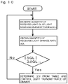
- the light transmittance of the dimmer may be equal to or smaller than a predetermined value (for convenience of description, may be referred to as a "first light transmittance").
- the measurement result of the light receiving element becomes equal to or smaller than a predetermined value (for convenience of description, may be referred to as a "second illumination measurement value)
- the light transmittance of the dimmer may be equal to or larger than a predetermined value (for convenience of description, can be referred to as a "second light transmittance").
- the light transmittance of the dimmer may be adjusted while monitoring the value of the illumination sensor (transmitted light illumination measuring sensor).
- the first illumination measurement value may be set to 10 lux
- the first light transmittance may be set to any value of 1% to 20%
- the second illumination measurement value may be set to 0.01 lux
- the second transmittance may be set to any value of 30% to 99%.
- the illumination measurement value of the quantity of received light (illumination) of the light receiving element is 1 ⁇ 10 -3 lux or less, for example, it is favorable to control a drive voltage of the dimmer to reduce a drive time, and to increase the light transmittance of the dimmer as fast as possible.
- the display devices according to the first to fourth embodiments of the present disclosure that includes the above-described various favorable embodiments or configurations, it is favorable to arrange the optical device and the dimmer in this order from the observer side.
- the dimmer and the optical device may be arranged in this order.
- the light receiving element in the display device according to the first to fourth embodiments of the present disclosure that includes the above-described various favorable embodiments may be formed of a known light receiving element (for example, a photodiode), and the light receiving element and the illumination sensor (transmitted light illumination measuring sensor) may be controlled by the light control device, for example.
- the light control device itself can be formed of a known control circuit.
- the quantity of received light change rate is calculated based on the quantity of received light measurement result of the light receiving element.
- the quantity of received light QL may be measured by the light receiving element for each (DELTA)t seconds (for example, 0.1 seconds).
- a change amount of the quantity of received light during (DELTA)t second is caused to be a quantity of received light change rate (DELTA)QL.
- a start time of the change of the quantity of received light (a timing when the change of the quantity of received light is started) is determined based on the quantity of received light measurement result of the light receiving element.
- the start time of the change of the quantity of received light may be caused to "0".
- Control of the light transmittance of the dimmer is started after elapse of a predetermined time from the start time of the change of the quantity of received light.
- the predetermined time as the predetermined time (so-called, a time lag), 0.2 to 0.3 seconds may be employed.
- the predetermined time may be made short.
- the highest light transmittance of the dimmer may be 30% or more, and the lowest light transmittance of the dimmer may be 20% or less.
- the upper limit of the highest light transmittance of the dimmer may be 99%, and the lower limit of the lowest light transmittance of the dimmer may be 1%.
- the light passing through the dimmer can be colored in desired color.
- the color to be colored by the dimmer can be variable, or the color to be colored by the dimmer can be fixed.
- the dimmer may be formed of a liquid crystal shutter that is capable of color display, or a dimmer to be colored in red, a dimmer to be colored in green, and a dimmer to be colored in blue may be layered.
- the color to be colored by the dimmer is not limited, but brown can be employed, for example.
- the dimmer may be detachably disposed or may be fixed in an area of the optical device from which light is emitted.
- the dimmer may be installed in the optical device using a screw made of transparent plastic, or the dimmer may be installed to a frame using a screw.
- a groove may be cut in the frame and the dimmer may be then engaged with the groove.
- a magnet may be installed in the frame, and the dimmer may be then installed to the frame.
- a sliding section may be provided in the frame, and the dimmer may be then inserted in the sliding section.
- a connector may be installed in the dimmer, and the dimmer may be then electrically connected to a light control device (for example, included in a control device that controls the image forming device) through the connector and a wire.
- the light receiving element may be installed to the dimmer, to the optical device, or to the frame, and an installation method may be a method suitable for the light receiving element in use.
- the transmitted light illumination measuring sensor may be installed to the optical device, or to the frame, and an installation method may be a method suitable for the transmitted light illumination measuring sensor in use.
- the optical device is a semi-transmissive type (see-through type). Specifically, at least a portion of the optical device that faces the eyes of the observer is adapted to be semi-transmissive (see-through), and it is possible to see an outside scene through this portion of the optical device.
- the display device may have one or two image display devices.
- the first deflection unit may reflect the light incident on the light guide plate, and the second deflection unit may transmit and reflect the light propagated inside the light guide plate with total reflection over a plurality of times. Further, in this case, the first deflection unit may function as a reflecting mirror, and the second deflection unit may function as a semi-transmissive mirror.
- the first deflection unit may be formed of metal including alloy, for example, or may be formed by a light reflection film (a kind of mirror) which reflects the light incident on the light guide plate or a diffraction grating (for example, hologram diffraction grating film) that diffracts the light incident on the light guide plate.
- the second deflection unit may be formed of a multi-layered structure in which a plurality of dielectric films are layered, a half mirror, a polarized beam splitter, or a hologram diffraction grating film. Further, the first and the second deflection units are disposed inside the light guide plate (incorporated inside the light guide plate).
- the first deflection unit parallel light incident on the light guide plate is reflected or diffracted so that the parallel light incident on the light guide plate is totally reflected inside the light guide plate.
- parallel light propagated inside the light guide plate with total reflection is reflected or diffracted over a plurality of times, and is then emitted from the light guide plate in the state of parallel light.
- the first deflection unit may diffract the light incident on the light guide plate
- the second deflection unit may diffract the light propagated inside the light guide plate with total reflection over a plurality of times.
- the first and the second deflection units may include a configuration of a diffraction grating element.
- the diffraction grating element may be formed of a reflective diffraction grating element or a transmissive diffraction grating element.
- one diffraction grating element may be formed of the reflective diffraction grating element and the other diffraction grating element may be formed of the transmissive diffraction grating element.
- an example of the reflective diffraction grating element includes a reflective volume hologram diffraction grating.
- the first deflection unit formed of the reflective volume hologram diffraction grating may be referred to as a "first diffraction grating member”
- the second deflection unit formed of the reflective volume hologram diffraction grating may be referred to as a "second diffraction grating member”.
- Image display of a single color may be performed by the image display device according to an embodiment of the present disclosure.
- P types of interference fringes may be formed in the first diffraction grating member or on the second diffraction grating member that includes one diffraction grating layer.
- a view angle may be equally divided into three, for example, and the first diffraction grating member or the second diffraction grating member can have a configuration made by diffraction grating layers corresponding to respective view angles being layered.
- the first diffraction grating member and the second diffraction grating member formed of a diffraction grating layer formed of a reflective volume hologram diffraction grating that diffracts and reflects the light having a red wavelength band (or, a wavelength) may be arranged in the first light guide plate
- the first diffraction grating member and the second diffraction grating member formed of a diffraction grating layer formed of a reflective volume hologram diffraction grating that diffracts and reflects the light having a green wavelength band (or a wavelength) may be arranged on the second light guide plate
- the first diffraction grating member and the second diffraction grating member formed of a diffraction grating layer formed of a reflective volume hologram diffraction grating that diffracts and reflects the light having a blue wavelength band(or, a wavelength) may be arranged on the third light guide plate, and these first
- the diffraction efficiency and the diffraction reception angle can be increased, and the diffraction angle can be optimized, when the light having each wavelength band (or, a wavelength) is diffracted and reflected in the first diffraction grating member or in the second diffraction grating member. It is favorable to arrange a protection member so that the reflective volume hologram diffraction grating does not directly contact with the air.
- the material that forms the first and the second diffraction grating members includes a photopolymer material.
- the material or basic structure that forms the first and the second diffraction grating member made of the reflective volume hologram diffraction grating may be the same as those of a reflective volume hologram diffraction grating in the related art.
- the reflective volume hologram diffraction grating refers to a hologram diffraction grating that diffracts and reflects only positive primary diffracted light.
- the interference fringes are formed over the front surface through the inside, and a method of forming the interference fringes may be the same as a forming method in the related art.
- a member (for example, photopolymer material) that forms the diffraction grating member may be irradiated with object light from a first predetermined direction on one side, and at the same time, the member that forms the diffraction grating member may be irradiated with reference light from a second predetermined direction on the other side, and the interference fringes formed by the object light and the reference light may be recorded inside the member that forms the diffraction grating member.
- the inclination angle of the interference fringes refers to an angle that is formed by the front surface of the diffraction grating member (or diffraction grating layer) and the interference fringes.
- the first and the second diffraction grating members are formed of a layered structure of the diffraction grating layers of P layers made of the reflective volume hologram diffraction grating
- layering of the diffraction grating layers may be achieved by individually manufacturing the diffraction grating layers of P layers and then by layering (adhering) the diffraction grating layers of P layers using an ultraviolet curing adhesive, for example.
- the diffraction grating layers of P layers may be manufactured by manufacturing one diffraction grating layer using an adhesive photopolymer material, and then, by sequentially attaching the adhesive photopolymer material thereon.
- the optical device may include a semi-transmissive mirror on which light emitted from the image forming device is incident and from which the light is then emitted toward the pupil of the observer.
- the light emitted from the image forming device may be propagated in the air and be incident on the semi-transmissive mirror.
- the light may be propagated inside a transparent member such as a glass plate or a plastic plate (specifically, a member formed of the same material as the material that forms the light guide plate described below), and may be then incident on the semi-transmissive mirror.
- the semi-transmissive mirror may be installed in the image forming device through this transparent member, or may be installed in the image forming device through a member different from the transparent member.
- the image forming device may have a plurality of pixels arranged in a two-dimensional matrix manner. Note that such a configuration of the image forming device is referred to as an "image forming device of a first configuration" for convenience of description.
- an image forming device formed of a reflective spatial light modulator and a light source for example, an image forming device formed of a reflective spatial light modulator and a light source; an image forming device formed of a transmissive spatial light modulator and a light source; or an image forming device formed of a light emitting element such as an organic EL (Electro Luminescence), an inorganic EL or a light emitting diode (LED) may be used.
- the image forming device formed of a reflective spatial light modulator and a light source is favorably used.
- a transmissive or reflective liquid crystal display such as a light bulb, for example or LCOS (Liquid Crystal On Silicon), or a digital micromirror device (DMD) may be used.
- the light source a light emitting element may be used.
- the reflective spatial light modulator may be formed of a polarized beam splitter that reflects a part of light from the liquid crystal display and the light source and guides it to the liquid crystal display, and transmits a part of the light reflected by the liquid crystal display and guides it to an optical system.
- the light emitting element that forms the light source a red light emitting element, a green light emitting element, a blue light emitting element, and a white light emitting element may be used. Further, red light, green light, and blue light emitted from the red light emitting element, the green light emitting element, and the blue light emitting element may be mixed and uniformized in brightness using a light pipe, to thereby obtain white light.
- the light emitting element for example, a semiconductor laser device, a solid laser or an LED may be used.
- the number of pixels may be determined based on a demanded specification in the image display device. As a specific value of the number of pixels, 320 X 240, 432 X 240, 640 X 480, 1024 X 768, 1920 X 1080 or the like may be used.
- the image forming device may have a configuration that includes a light source and a scanning section that scans parallel light emitted from the light source. Note that, such a configuration of the image forming device is referred to as an "image forming device of a second configuration" for convenience of description.
- a light emitting element may be used as the light source in the image forming device of the second configuration. Specifically, a red light emitting element, a green light emitting element, a blue light emitting element, and a white light emitting element may be used. Further, red light, green light, and blue light which are emitted from the red light emitting element, the green light emitting element, and the blue light emitting element are mixed and uniformized in brightness using a light pipe, to thereby obtain white light.
- the light emitting element for example, a semiconductor laser device, a solid laser or an LED may be used.
- the number of pixels (virtual pixels) in the image forming device of the second configuration may be determined based on a demanded specification in the image display device.
- 320 X 240, 432 X 240, 640 X 480, 1024 X 768, 1920 X 1080 or the like may be used.
- color composition is favorably performed using a cross prism.
- MEMS Micro Electro Mechanical Systems
- MEMS Micro Electro Mechanical Systems which scans light emitted from the light source horizontally and vertically, for example, which has a micromirrors or Galvano mirrors which are able to rotate in two-dimensional directions may be used.
- the optical system an optical system that collimates emitted light into parallel light, which may be referred to as a "parallel light emitting optical system", and specifically, for example, a collimating optical system or a relay optical system
- a request of the parallel light is based on the fact that it is necessary that light wave surface information at the time when the light is incident on the light guide plate be stored even after the light is emitted from the light guide plate through the first deflection unit and through the second deflection unit.
- a light outputting section of the image forming device may just be disposed at a position of the focal distance in the parallel light emitting optical system, for example.
- the parallel light emitting optical system has a function to convert pixel position information into angle information in the optical system of the optical device.
- an optical system that has a generally positive optical power which individually uses or combines a convex lens, a concave lens, a free-form surface prism and a hologram lens may be used.
- a light shielding section that includes an opening section may be arranged between the parallel light emitting optical system and the light guide plate to prevent undesired light from being emitted from the parallel light emitting optical system and incident on the light guide plate.
- the light guide plate includes two parallel surfaces (a first surface and a second surface) that extend in parallel with an axis line (X axis) of the light guide plate.
- a surface of the light guide plate that light is incident on is referred to as a light guide plate incident surface
- a surface of the light guide plate from which light is emitted is referred to as a light guide plate emitting surface
- the light guide plate incident surface and the light guide plate emitting surface may be formed by the first surface, or the light guide plate incident surface may be formed by the first surface and the light guide plate emitting surface may be formed by the second surface.
- the material that forms the light guide plate examples include glass including optical glass such as quartz glass or BK7, and a plastic material (for example, PMMA, polycarbonate resin, acrylic based resin, amorphous polypropylene based resin, or styrene based resin which includes AS resin).
- the light guide plate is not limited to a flat plate, and may have a curved plate.
- the frame is favorably formed into a pair of glasses (spectacle type), and specifically, the frame can be formed of a front section arranged in front of the observer, and two temple sections rotatably attached to both ends of the front section through hinges. An end cover section is attached to a tip end portion of each temple section.
- the image forming device is installed to the frame. Specifically, for example, the image forming device may be installed in the temple section. Further, the front section and the two temple sections may be integrally formed. That is, when the overall display device of the present disclosure is viewed, the frame has the same structure as that of normal glasses.
- the material that forms the frame including a pad section may be formed of the same material as the material which forms the normal glasses, such as metal, alloy, plastic or a combination thereof.
- a nose pad may be installed to the front section. That is, when the overall display device of the present disclosure is viewed, an assembly of the frame and the nose pad has approximately the same structure as that of normal glasses, except that there is no rim.
- the nose pad may have a known configuration or structure.
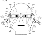
- each image forming device may include a headphone section, and a headphone section wire from each image forming device may extend to the headphone section from the tip end portion of the end cover section through the temple section and the inside of the end cover section.
- the headphone section for example, an inner ear type or a canal type of headphone section may be used. More specifically, it is favorable that the headphone section wire extends to the headphone section by wrapping around an auricle from the tip end portion of the end cover section.
- an imaging device may be installed in the central part of the front section.
- the imaging device may be formed of a solid state imaging device made of a CCD or CMOS sensor, and a lens, for example.
- a wire from the imaging device may be connected to one image display device (or image forming device) through the front section, for example, and may be further included in a wire that extends from the image display device (or image forming device).
- central light rays Light rays which emitted from the center of the image forming device and pass through a node of the optical system on the side of the image forming device are called "central light rays”. A light ray that perpendicularly is incident on the optical device among the central light rays is called “central incident light ray”.
- a point of the optical device that the central incident light ray is incident on is represented as an optical device central point
- an axis line that passes through the optical device central point and is parallel to an axis line direction of the optical device (to be specific, the light guide plate) is represented as the X axis
- an axis line that passes through the optical device central point and coincides with a normal line of the optical device (to be specific, the light guide plate) is represented as the Y axis.
- the horizontal direction in the display device according to an embodiment of the present disclosure is a direction parallel to the X axis, and may be referred to as an "X axis direction".
- the optical system is disposed between the image forming device and the optical device, and collimates the light emitted from the image forming device into parallel light. Further, light flux which is collimated as parallel light by the optical system is incident on the optical device, is guided therein, and is then emitted therefrom.
- a central point of the first deflection unit is referred to as an "optical device central point".
- the central incident light ray may intersect with the XY plane at an angle (theta) other than 0 degrees. Accordingly, limitation to the installation angle of the image display device when the image display device is installed in the installation section of the frame can be reduced and a high degree of freedom in design can be obtained. Further, in this case, the central incident light ray may be included in the YZ plane, which is favorable from the point of view of easy handling, setting or installation of the image display device. Further, the optical axis of the optical system can be included in the YZ plane, and may intersect with the XY plane at an angle other than 0 degrees.
- the optical axis of the optical system may be parallel to the YZ plane and to the XY plane, and may pass through a position away from the center of the image forming device.
- the angle (theta) where the central incident light ray intersects with the XY plane may be an elevation angle. That is, the central incident light ray may be directed to the XY plane from below the XY plane, and may collide with the XY plane.
- the XY plane favorably intersects with the vertical plane at an angle other than 0 degrees, and the XY plane more favorably intersects with the vertical plane at an angle (theta)'.
- the maximum value of the angle (theta)' may be 5 degrees although it is not limited to the value.
- the horizontal plane is a plane in which the line of vision ("horizontal line of vision of an observer") when the observer views an object (for example, an object on an infinitely distant side in the horizontal direction such as a skyline or sealine) positioned in the horizontal direction and two pupils of the observer horizontally positioned are included.
- the vertical plane is a plane perpendicular to the horizontal plane.
- a central incident light ray emitted from the optical device and to be incident on the pupils of the observer may form a depression angle.
- the depression angle with reference to the horizontal plane for example, 5 to 45 degrees may be used.
- the display device may be used in, for example, display of various explanations, marks, symbols, signs, emblems, designs or the like in operation, manipulation, maintenance, disassembly or the like of observation objects such as various apparatuses; display of maps; display of road information, route guide information, or traffic information; display of various explanations, marks, symbols, signs, emblems, designs or the like related to observation objects such as people or goods; display of moving images or still images; display of subtitles in a movie or the like; display of explanatory notes or closed captions related to images which are synchronized with the images; or display of various explanations related to observation objects, or explanatory notes or the like for describing their content, progress, background or the like, in plays or Kabukis, Nohs, Noh farces, operas, concerts, ballets, various plays, amusement parks, art museums, sightseeing areas, tourist resorts, visitor information, or may also be used for display of closed captions.
- characters may be displayed in the display device as images related to the observation objects at an appropriate timing.
- an image control signal is transmitted to the display device by operation of an operator or under the control of a computer or the like, based on a predetermined schedule or time allocation, according to the progress of a movie, play or the like, so that an image is displayed in the display device.
- the display device may be used as a stereopsis display device.
- a polarizing plate or a polarizing film may be detachably installed in the optical device, or may be attached to the optical device.
- the image signal input to the image forming device may include brightness data (brightness information) or chromaticity data (chromaticity information) related to images to be displayed, or both of the brightness data and the chromaticity data, in addition to the image signal (for example, character data).
- the brightness data may be brightness data corresponding to brightness of a predetermined area that includes an observation object when seen through the optical device
- the chromaticity data may be chromaticity data corresponding to chromaticity of the predetermined area that includes the observation object when seen through the optical device. In this way, by including the brightness data related to an image, it is possible to control the brightness (luminance) of an image to be displayed.
- the chromaticity data related to the image it is possible to control the chromaticity (color) of the image to be displayed.
- the brightness data and the chromaticity data related to the image it is possible to control the brightness (luminance) and the chromaticity (color) of the image to be displayed.
- the brightness data is brightness data corresponding to the brightness of the predetermined area that includes the observation object when seen through the optical device
- the value of brightness data may just be set so that the value of brightness of an image becomes high (that is, so that the image is displayed brightly) as the value of brightness of the predetermined area that includes the observation object when seen through the optical device becomes higher.
- the value of chrominance data may just be set so that the chrominance of the predetermined area that includes the observation object when seen through the optical device and the chrominance of the image to be displayed form an approximately complementary color relationship.
- complementary colors represent a set of colors having the relationship of opposite positions in the color circle. For example, red and green, yellow and violet, blue and orange, or the like form the complementary colors.
- the complementarity of a visual effect when colors are arranged in parallel is different from the complementarity of a visual effect when colors are mixed with each other.
- These colors are called, the complementary colors, contrast colors or opponent colors.
- the opponent colors directly indicate a color that is opposite to a complementary color
- the range of colors indicated by the complementary colors is slightly broad.
- Combination of the complementary colors has a synergy effect of using the mutual colors, which is called a complementary color harmony.
- Example 1 relates to a display device according to the first and second embodiments of the present disclosure.
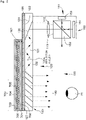
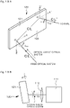
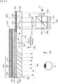
- Fig. 1A illustrates a schematic diagram of the display device of Example 1 (specifically, a head-mounted display, HMD), as viewed from above
- Fig. 1B illustrated a block diagram of the light control device (color control circuit)
- Fig. 2 illustrates a conceptual diagram of the image display device of Example 1
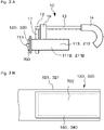
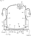
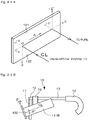
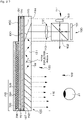
- Fig. 3A illustrates a schematic diagram, as viewed from the side
- Fig. 3B illustrates a schematic diagram of the optical device and a part of the dimmer, as viewed from the front
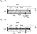
- Figs. 4A and 4B illustrate schematic cross-sectional views of the dimmer schematically illustrating the behavior of the dimmer in the display device of Example 1
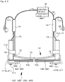
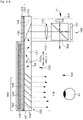
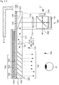
- Fig. 5 illustrates a diagram of a state where the display device of Example 1 is mounted on the head of the observer, as viewed from above (note that, only the image display device is illustrated and the frame and the like are o
- the display device includes
- An image display device 100, 200, 300, 400 or 500 according to Example 1, or any one of Examples 2 to 15 described below includes
- the display device according to Example 1 includes
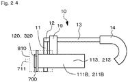
- the dimmer 700 is disposed on the side opposite to the image forming device 111 or 211 of the optical device 120, 320, or 520.
- the dimmer 700 that is a kind of optical shutter is fixed to the optical device 120, 320, or 520 (specifically, a protection member (protection plate) 126 or 326 that protects the light guide plate 121 or 321, or the semi-transmission mirror 520) using an adhesive 707.
- the dimmer 700 is arranged in an area of the optical device 120, 320, or 520 on a side opposite to the observer 20.
- the protection member (protection plate) 126 or 326 adhere to the second surface 123 or 323 of the light guide plate 121 or 321 with the adhesive member 127 or 327.
- the light receiving element 711 formed of a photodiode is arranged on an outside end part of the optical device 120 or 320 (specifically, on the outside end part of the light guide plate 121 or 321).
- the light receiving element 711 is connected to the light control device 18A through a connector or a wire (not illustrated). Specific operations of the light receiving element 711 and the dimmer 700 will be described below.
- the optical device 120 or 320 according to Example 1, or any one of Example 2 to 4, and 6 to 15 described below includes
- the first deflection unit 130 and the second deflection unit 140 are disposed inside the light guide plate 121. Further, the first deflection unit 130 reflects light incident on the light guide plate 121, and the second deflection unit 140 transmits and reflects the light propagated inside the light guide plate 121 with total reflection over a plurality of times. That is, the first deflection unit 130 functions as a reflecting mirror, and the second deflection unit 140 functions as a semi-transmissive mirror. More specifically, the first deflection unit 130 installed in the light guide plate 121 is formed by a light reflection layer (a kind of mirror) made of aluminum (Al) and reflects the light incident on the light guide plate 121.
- a light reflection layer a kind of mirror
- the second deflection unit 140 provided inside the light guide plate 121 is formed by a multi-layered structure in which a plurality of dielectric films are layered.
- the dielectric film includes a TiO 2 film that is a high dielectric constant material and a SiO 2 film that is a low dielectric constant material, for example.
- the multi-layered structure in which the plurality of dielectric films are layered is disclosed in JP 2005-521099 W . In the figure 6 -layered dielectric films are illustrated, but it is not limited to the example. A thin piece formed of the same material as the material which forms the light guide plate 121 is interposed between the dielectric films.
- the parallel light incident on the light guide plate 121 is reflected (or diffracted) so that the parallel light incident on the light guide plate 121 is totally reflected inside the light guide plate 121.
- the parallel light propagated inside the light guide plate 121 with total reflection is reflected (or diffracted) over a plurality of times, and is emitted from the light guide plate 121 toward the pupil 21 of an observer 20 in the state of parallel light.
- the first deflection unit 130 may be installed by cutting a portion 124 of the light guide plate 121 where the first deflection unit 130 is to be installed to form an inclination surface on which the first deflection unit 130 is to be formed in the light guide plate 121, by forming a light reflection film on the inclination surface by vacuum deposition, and then, by allowing the cut portion 124 of the light guide plate 121 to adhere to the first deflection unit 130.
- the second deflection unit 140 may be installed by manufacturing a multi-layered structure obtained by layering a plurality of combinations of the same material (for example, glass) as the material that forms the light guide plate 121 and an dielectric film (which may be formed by vacuum deposition, for example), by cutting a portion 125 of the light guide plate 121 where the second deflection unit 140 is to be installed to form an inclination surface, by allowing the multi-layered structure to adhere to the inclination surface, and by performing polishing or the like to shape its appearance.
- the optical device 120 in which the first deflection unit 130 and the second deflection unit 140 are installed inside the light guide plate 121 can be obtained.
- the light guide plate 121 or 321 formed of an optical glass or plastic material includes two parallel surfaces (a first surface 122 or 322 and a second surface 123 or 323) that extend in parallel in the light propagation direction (X axis) inside the light guide plate 121 or 321 with total reflection.
- the first surface 122 or 322 faces the second surface 123 or 323.
- parallel light is incident on the first surface 122 or 322 corresponding to a light incident surface, is propagated inside with total reflection, and is then emitted through the first surface 122 and 322 corresponding to a light emitting surface.
- the configuration is not limited thereto, and thus, the light incident surface may be formed by the second surface 123 or 323, and the light emitting surface may be formed by the first surface 122 or 322.
- the image forming device 111 is an image forming device of a first configuration, and includes a plurality of pixels that are arranged in a two-dimensional matrix form.
- the image forming device 111 includes a reflective spatial light modulator 150 and a light source 153 that includes a light emitting diode that emits white light.
- Each image forming device 111 is accommodated in a housing 113 (indicated by a dashed line in Fig. 1 ), and an opening section (not illustrated) is formed in the housing 113.
- Light is emitted from the optical system 112 (parallel light emitting optical system, collimating optical system) through the opening section.
- the reflective spatial light modulator 150 includes a liquid crystal display (LCD) 151 formed by LCOS that is a light bulb, and a polarized beam splitter 152 that reflects a part of light from the light source 153 to guide the reflected light to the liquid crystal display 151, and transmits part of the light reflected by the liquid crystal display 151 and guides the transmitted light to the optical system 112.
- the liquid crystal display 151 includes a plurality of (for example, 640 X 480) pixels (liquid crystal cells) which are arranged in the two-dimensional matrix form.
- the polarized beam splitter 152 has a known structure. Non-polarized light which is emitted from the light source 153 collides with the polarized beam splitter 152.
- a P-polarized component passes therethrough and is emitted to the outside. Meanwhile, an S-polarized component is reflected in the polarized beam splitter 152, is incident on the liquid crystal display 151, is reflected inside the liquid crystal display 151, and is then emitted from the liquid crystal display 151.
- a large amount of P-polarized components are included in light output from pixels that display "white”
- a large amount of S-polarized components are included in light output from pixels that display "black”.
- the optical system 112 includes a convex lens, for example.
- the image forming device 111 (more specifically, the liquid crystal display 151) is disposed in the position of the focal distance in the optical system 112 in order to generate parallel light.
- the frame 10 formed of a spectacle type frame includes a front section 11 that is arranged in front of an observer 20, two temple sections 13 that are rotatably installed at opposite ends of the front section 11 through hinges 12, and an end cover section 14 (also referred to as a tip, earmuff or ear pad) that is installed in a tip end portion of each temple section 13. Further, a nose pad (not illustrated) is installed. That is, an assembly of the frame 10 and the nose pad basically has approximately the same structure as in normal glasses. Further, each housing 113 is detachably installed in or fixed to the temple section 13 by an installation member 19.
- the frame 10 is formed of metal or plastic. Each housing 113 may be installed the temple section 13 by the installation member 19 so as not to able to be detached from the temple section 13.
- each housing 113 may be detachably installed at the temple section of a frame owned by the observer 20 by the installation member 19. Further, each housing 113 may be installed outside the temple section 13, or may be installed inside the temple section 13.
- a wire (signal line, power line or the like) 15 that extends from one image forming device 111A extends outside from the tip end portion of the end cover section 14 through the temple section 13 and the inside of the end cover section 14, and is connected to a control device (control circuit, control section) 18.
- each of the image forming devices 111A and 111B includes a headphone section 16, and a headphone section wire 17 that extends from each of the respective image forming devices 111A and 111B extends to the headphone section 16 from the tip end portion of the end cover section 14 through the temple section 13 and the inside of the end cover section 14.
- the headphone section wire 17 extends to the headphone section 16 so as to wrap around an auricle from the tip end portion of the end cover section 14. With such a configuration, without giving an impression that the headphone section 16 or the headphone section wire 17 are disorderedly arranged, it is possible to achieve a clean display device.
- the dimmer 700 in Example 1 is formed of an optical shutter made of the liquid crystal shutter, to be specific, formed such that the light transmission control material layer 705 is formed of a liquid crystal material layer. That is, the dimmer 700 is formed of
- the first substrate 701 and the second substrate 703 are formed of a plastic material.
- the first electrode 702 and the second electrode 704 are formed of a transparent electrode formed of an indium-tin oxide (ITO), and are formed based on a combination of a PVD method such as a sputtering method and a lift-off method.
- the light transmission control material layer 705 is formed of a liquid crystal material layer formed of a TN (twisted nematic) liquid crystal material.
- the first electrode 702 and the second electrode 704 are not patterned, and are so-called solid electrodes.
- the first electrode 702 and the second electrode 704 are connected to the light control device 18A through a connector, or a wire (not illustrated).
- Outer edge portions of the two substrates 701 and 703 are sealed by a sealant 706. Further, the first substrate 701 and the protection member 126 (that protects the light guide plate 121) of the dimmer 700 adhere to each other by the adhesive 707. In addition, polarizing films are attached to the outer surfaces of the first substrate 701 and the second substrate 703. However, illustration of the polarizing films is omitted.
- the first substrate 701 of the dimmer 700 is made shorter than the light guide plate 121, and the first substrate 701 of the dimmer 700 is fixed to the protection member 126 by the adhesive 707.
- the adhesive 707 is arranged on an outer edge portion of the first substrate 701. The same applies to Examples 2 to 15 described below.
- the optical device 120 and the dimmer 700 are arranged in that order from the observer side.
- the light transmittance of the dimmer 700 can be controlled by a voltage applied to the first electrode 702 and the second electrode 704. To be specific, for example, when the voltage is applied to the first electrode 702 while the second electrode 704 is grounded, the arrangement state of the liquid crystal in the liquid crystal material layer that forms the light transmission control material layer 705 is changed, and the light transmittance of the liquid crystal material layer is changed (see Figs. 4A and 4B ).
- the light control device 18A calculates a quantity of received light change rate based on the quantity of received light measurement result of the light receiving element 711, determines a light transmittance change rate in the dimmer 700 based on the quantity of received light change rate, and controls light transmittance of the dimmer 700 based on the determined light transmittance change rate.
- the light control device 18A determines a start time of a change of the quantity of received light (a time when the change of the quantity of received light is started) based on the quantity of received light measurement result of the light receiving element 711, and starts control of the light transmittance of the dimmer 700 after elapse of a predetermined time from the start time of the change of the quantity of received light.
- the light receiving element 711 measures the quantity of light of an outside area corresponding to a background of an image to be observed by the observer 20 in the optical device 120, 320, or 520 (for example, the space area indicated by "A" in Fig. 5 ).
- the light receiving element 711 includes directivity to light to be received. Specifically, by arranging a lens (not illustrated) on the light incident side of the light receiving element 711, the directivity to the light to be received is provided to the light receiving element 711.
- the light control device 18A includes a table related to a relationship between the quantity of received light change rate and the light transmittance change rate in the dimmer 700.
- This table is created based on the change of the pupil (pupil diameter) of the observer 20 that follows the change of the quantity of light incident from an outside. Specifically, the relationship between the change of the quantity of light and the change of the pupil (pupil diameter) is checked using an optical device called iriscorder that can measure the change of the pupil (pupil diameter) of a human with respect to photo stimulation, or based on a simplified measurement by an infrared camera, obtains a table related to the relationship between the quantity of received light change rate and the light transmittance change rate in the dimmer 700, and may store the table in a memory of the light control device 18A.
- the light control device 18A that controls the light receiving element 711 and the dimmer 700 is formed of a quantity of received light operation circuit, a memory, and a light transmittance control circuit.
- the quantity of received light operation circuit receives a quantity of received light measurement value from the light receiving element 711, obtains the quantity of received light (illumination), and further obtains the quantity of received light change rate (DELTA)QL.
- the memory stores the table related to the relationship between the quantity of received light change rate (DELTA)QL and the light transmittance change rate (DELTA)Tr in the dimmer.
- the light transmittance control circuit determines the light transmittance change rate (DELTA)Tr based on the quantity of received light change rate (DELTA)QL, and controls the light transmittance of the dimmer based on the determined light transmittance change rate (DELTA)Tr. Further, as needed, the light control device 18A may employ a configuration that includes a comparison operation circuit that compares the obtained quantity of received light (illumination) and a standard value, and the second control circuit that controls the dimmer 700 or/and the image forming device 111 or 211 based on a value obtained by the comparison operation circuit. These circuits may be formed of a known circuit. In controlling the dimmer 700, the light transmittance of the dimmer 700 is controlled.
- brightness of an image to be formed in the image forming device 111 or 211 is controlled.
- the control of the light transmittance in the dimmer 700 and the control of the brightness of an image in the image forming device 111 or 211 may be independently performed, or may be collectively performed.
- FIG. 10 A flowchart illustrating a procedure to determine the light transmittance of the dimmer is illustrated in Fig. 10 .
- a relationship [t, (DELTA)QL t , and (DELTA)Tr t ] between a change amount (DELTA)QL t of the quantity of received light for each 0.1 seconds after a change is caused in the quantity of received light and the light transmittance change rate (DELTA)Tr t in the dimmer is obtained in advance, or determined in advance, and for example, the table is stored in the memory provided in the light control device 18A.
- Whether the change is caused in the quantity of received light is determined whether the quantity of received light change rate (DELTA)QL becomes a threshold (DELTA)QL th of the quantity of received light change rate set in advance or more, by the light control device 18A.
- the light transmittance control circuit of the light control device 18A determines the quantity of received light change rate (DELTA)QL has become the threshold (DELTA)QL th set in advance or more
- the light transmittance control circuit reads out the light transmittance change rate (DELTA)Tr t from the table that stores the relationship [t, (DELTA)QL t , and (DELTA)Tr t ] between the quantity of received light change rate (DELTA)QL and the light transmittance change rate (DELTA)Tr in the dimmer and determines the light transmittance Tr.
- the light transmittance control circuit then control the light transmittance of the dimmer 700 based on the determined light transmittance Tr.
- a start time of the change of the quantity of received light is determined based on the measurement result of the quantity of received light QL of the light receiving element 711.
- the quantity of received light change rate (DELTA)QL obtained from the quantity of received light measurement result of the light receiving element 711 becomes the threshold (DELTA)QL th set in advance or more
- the start time of the change of the quantity of received light is caused to be "0".
- the control of the light transmittance in the dimmer 700 is started after elapse of a predetermined time after the start time of the change of the quantity of received light.
- the predetermined time time lag
- a first stage (the period of "a” to “b” if Fig. 6A ); a second stage (the period of "b” to “c” in Fig. 6A ); a third stage (the period of "c” to “d” in Fig. 6A ); a fourth stage (the period of "d” to "e” in Fig. 6A ); a fifth stage (the period of "e” to “f” in Fig. 6A ); a sixth stage (the period of "f” to “g” in Fig. 6A ); and a seventh stage (the period of "g” to “h” in Fig. 6A ).
- a state in which a vehicle in traveling gets out of a tunnel, and immediately after, is incident on a tunnel again, a state of momentarily receiving light, or a state of momentarily glancing sunlight reflected on a mirror or a glass can be assumed.
- the quantity of received light is sharply increased from a quantity of received light QL 0 of an initial state (here, (DELTA)QL t is approximately equal to 0) to QL 1 .
- the time length of the first stage is 0.1 seconds.
- the time indicated by "a” corresponds to a first start time of the change of the quantity of received light.
- a reference of an elapsed time is the first start time of the change of the quantity of received light.
- the light transmittance takes a value Tr 0 of an initial state.
- the first and second stages correspond to the predetermined time (time lag), and the total time length of the first and second stages is 0.3 seconds.
- the light transmittance keeps the value Tr 0 of the initial state.
- the quantity of received light is sharply decreased from the quantity of received light QL 1 to QL 0 .
- the time indicated by "e” corresponds to a second start time of the change of the quantity of received light.
- the light transmittance keeps the value Tr 1 .
- the sixth stage (the period of "f” to "g” in Fig. 6A , and after elapse of 2.1 second to elapse of 2.3 seconds), there is no change in the quantity of received light QL 0 .
- the light transmittance keeps the value Tr 1 .
- the fifth and sixth stages correspond to the predetermined time (time lag), and the total time length of the fifth and sixth stages is 0.3 seconds.
- the value of the light transmittance Tr is slowly increased, and the light transmittance Tr is returned to the value Tr 0 of the initial state at the end of the seventh stage.
- in the seventh stage is more slowly than the change of the value
- the example illustrated in Fig. 6B shows an inverse increase/decrease state of the change state of the quantity of received light and the quantity of received light change rate, and the change state of the light transmittance and the light transmittance change rate, with the example illustrated in Fig. 6A .
- a first stage (the period of "a” to “b” if Fig. 7A ); a second stage (the period of "b” to “c” in Fig. 7A ); a third stage (the period of "c” to “d” in Fig. 7A ); and a fourth stage (the period of "d” and subsequent period in Fig. 7A ).
- a state in which a vehicle in traveling gets out of a tunnel a state in which a vehicle in traveling is incident on a tunnel, a state of continuously receiving light, or a state of continuously viewing sunlight reflected on a mirror or a glass can be assumed.
- the quantity of received light is sharply increased from a quantity of received light QL 0 of an initial state (here, (DELTA)QL t is approximately equal to 0) to QL 1 .
- the time length of the first stage is 0.1 seconds.
- the time indicated by "a” corresponds to a start time of the change of the quantity of received light.
- a reference of an elapsed time is the start time of the change of the quantity of received light.
- the light transmittance takes a value Tr 0 of an initial state.
- the first and second stages correspond to the predetermined time (time lag), and the total time length of the first and second stages is 0.3 seconds.
- the light transmittance keeps the value Tr 0 of the initial state.
- Fig. 7B shows an inverse increase/decrease state of the change state of the quantity of received light and the quantity of received light change rate, and the change state of the light transmittance and the light transmittance change rate, with the example illustrated in Fig. 7A .
- a first stage (the period of "a” to “b” if Fig. 8A ); a second stage (the period of "b” to “c” in Fig. 8A ); a third stage (the period of "c” to “d” in Fig. 8A ); a fourth stage (the period of "d” to “e” in Fig. 8A ); and a fifth stage (the period of "e” to “f” in Fig. 8A ).
- the quantity of received light QL is increased from the quantity of received light QL 0 of an initial state (here, (DELTA)QL t is approximately equal to 0).
- is smaller than
- the time length of the first stage is 0.3 seconds.
- the time indicated by "a” corresponds to a first start time of the change of the quantity of received light.
- a reference of an elapsed time is the first start time of the change of the quantity of received light.
- the light transmittance takes a value Tr 0 of an initial state.
- the quantity of received light QL is continuously increased, and becomes QL 1 at the end of the second stage.
- is started to change.
- is smaller than
- the value of the light transmittance is decreased from Tr 0 to Tr 1 from the start to the end of the second stage.
- the quantity of received light QL is started to decrease.
- the time indicated by "c” corresponds to a second start time of the change of the quantity of received light.
- the value of the light transmittance is slowly and continuously decreased.
- the quantity of received light QL 1 is continuously decreased, and becomes the quantity of received light QL 0 at the end of the fourth stage.
- the value of the light transmittance Tr is slowly increased.
- in the fourth stage is more slowly changed than
- Fig. 8B shows an inverse increase/decrease state of the change state of the quantity of received light and the quantity of received light change rate, and the change state of the light transmittance and the light transmittance change rate, with the example illustrated in Fig. 8A .
- a first stage (the period of "a” to "b” if Fig. 9A ); a second stage (the period of "b” to “c” in Fig. 9A ); and a third stage (the period of "c" and a subsequent period in Fig. 9A ).
- the quantity of received light QL is increased from the quantity of received light QL 0 of an initial state (here, (DELTA)QL t is approximately equal to 0).
- is smaller than
- the time length of the first stage is 0.3 seconds.
- the time indicated by "a” corresponds to a start time of the change of the quantity of received light.
- a reference of an elapsed time is the start time of the change of the quantity of received light.
- the light transmittance takes a value Tr 0 of an initial state.
- the quantity of received light QL is continuously increased, and becomes QL 1 at the end of the second stage.
- is started to change.
- is smaller than
- the value of the light transmittance is decreased from Tr 0 to Tr 1 from the start to the end of the second stage.
- Fig. 9B shows an inverse increase/decrease state of the change state of the quantity of received light and the quantity of received light change rate, and the change state of the light transmittance and the light transmittance change rate, with the example illustrated in Fig. 9A .
- the illumination of the environment where the display device is placed may be measured by the light receiving element 711 or an illumination sensor (environment illumination measuring sensor) that is different from the light receiving element 711, the light transmittance of the dimmer 700 may be controlled by the comparison operation circuit and the second control circuit based on the measurement result, and the brightness of an image formed by the image forming device 111 or 211 may be collectively or independently controlled based on the measurement result of the light receiving element 711 or the environment illumination measuring sensor.
- the environment illumination measuring sensor may be arranged on an outside end part of the optical device 120 or 320 (to be specific, on the outside end part of the light guide plate 121 or 321), for example.
- the quantity of received light change rate (DELTA)QL does not exceed the threshold (DELTA)QL th set in advance, but the quantity of received light QL is gradually changed. That is, a change is caused in the quantity of received light QL 0 of the initial state.
- the obtained quantity of received light (illumination) is compared with a standard value in the comparison operation circuit of the light control device 18A, and the light transmittance of the dimmer 700 may be controlled by the second control circuit based on a value obtained by the comparison operation circuit.
- the light transmittance of the dimmer 700 is caused to the a predetermined value (first light transmittance)or less.
- the measurement result of the light receiving element 711 is a predetermined (second illumination measurement value) or less
- the light transmittance of the dimmer 700 is caused to be a predetermined value (second light transmittance) or more.
- the first illumination measurement value may be set to 10 lux
- the first light transmittance may be set to any value of 1% to 20%
- the second illumination measurement value may be set to 0.01 lux
- the second transmittance may be set to any value of 30% to 99%.
- the brightness of an image formed in the image forming device 111 or 211 may be performed.
- the control of the light transmittance in the dimmer 700 and the control of the brightness of an image in the image forming device 111 or 211 may be independently performed, or may be collectively performed. In this way, if the light transmittance of the dimmer is controlled and the brightness of an image formed by the image forming device is controlled based on the measurement result of the light receiving element 711 or the environment illumination measuring sensor, not only high contrast can be provided to an image observed by the observer 20, but also an observation state of the image can be optimized depending on the illumination of surrounding environment of the display device.
- the light control device calculates a quantity of received light change rate based on a quantity of received light measurement result of the light receiving element, determines a light transmittance change rate in the dimmer based on the quantity of received light change rate, and controls light transmittance of the dimmer based on the determined light transmittance change rate. Therefore, a display device that provides the observer who wears the display device with a less unpleasant feeling and that does not force the eyes to bear substantial burden can be provided even if the quantity of incident light from an outside is changed.
- the light control device determines a start time of a change of a quantity of received light based on a quantity of received light measurement result of the light receiving element, and starts control of light transmittance of the dimmer after elapse of a predetermined time from the start time of the change of the quantity of received light. Therefore, a display device that provides the observer who wears the display device with a less unpleasant feeling and that does not force the eyes to bear substantial burden can be provided even if the quantity of incident light from an outside is changed. Furthermore, the light transmittance of the dimmer is controlled based on the quantity of received light measurement result of the light receiving element. Therefore, the overall structure of the display device can be simplified, and high contrast can be provided to an image observed by the observer. In addition, for example, an observation state of the image can be optimized depending on the illumination of surrounding environment of the display device.
- Example 2 is a modification example of Example 1.
- Fig 11 is a conceptual diagram illustrating an image display device 200 in a display device (head mounted display) according to Example 2.
- an image forming device 211 includes an image forming device of a second configuration. That is, the image forming device 211 includes a light source 251, and a scanning section 253 that scans parallel light emitted from the light source 251. More specifically, the image forming device 211 includes
- the light source 251 includes a light emitting element which emits white color. Further, light emitted from the light source 251 is incident on the collimating optical system 252 that has a positive optical power as a whole, and is then output as parallel light. Further, this parallel light is reflected by a total reflection mirror 256, and is subject to horizontal scanning and vertical scanning by the scanning section 253 that includes a MEMS in which micromirrors are rotatably arranged in two-directional directions and incident parallel light is able to be scanned in a two-directional manner, to become a kind of two-dimensional image to generate virtual pixels (in which the number of pixels may be the same as in Example 1, for example). Further, light from the virtual pixels passes through the relay optical system (parallel light emitting optical system) 254 that is formed by a known relay optical system, and light flux that has been collimated into parallel light is incident on an optical device 120.
- the relay optical system parallel light emitting optical system
- the optical device 120 on which light flux collimated into parallel light by the relay optical system 254 is incident, in which the light is guided, and from which the light is emitted has the same configuration or structure as that of the optical device described in Example 1, its detailed description will be omitted. Further, since the display device according to Example 2 has substantially the same configuration or structure as that of the display device in the first embodiment except that the image forming device 211 of a different type is used as described above, its detailed description will be omitted.
- Example 3 is a modification example of Example 1.
- Fig. 12 is a conceptual diagram illustrating the image display device 300 in a display device (head mounted display) according to Example 3.
- Fig. 13 is an enlarged cross-sectional view schematically illustrating a part of a reflective volume hologram diffraction grating.
- the image forming device 111 includes an image forming device of a first configuration.
- an optical device 320 has substantially the same basic configuration or structure as that of the optical device 120 in Example 1, except that a first deflection unit and a second deflection unit of a different configuration or structure are used.
- the first deflection unit and the second deflection unit are disposed on a front surface (specifically, a second surface 323 of a light guide plate 321) of the light guide plate 321. Further, the first deflection unit diffracts light incident on the light guide plate 321, and the second deflection unit diffracts light propagated inside the light guide plate 321 with total reflection over a plurality of times.
- the first deflection unit and the second deflection unit include a diffraction grating element, specifically, a reflective diffraction grating element, and more specifically, a reflective volume hologram diffraction grating.
- first deflection unit formed by the reflective volume hologram diffraction grating is referred to as a "first diffraction grating member 330”
- second deflection unit formed by the reflective volume hologram diffraction grating is referred to as a "second diffraction grating member 340" for convenience of description.
- the first diffraction grating member 330 and the second diffraction grating member 340 have a configuration in which one diffraction grating layer is layered. Interference fringes corresponding to one type of wavelength band (or wavelength) are formed in each diffraction grating layer made of a photopolymer material, which is manufactured by a method in the related art.
- the pitch of the interference fringes formed in the diffraction grating layer (diffraction optical element) is constant, and the interference fringes are linear and are in parallel with the Z axis.
- axis lines of the first diffraction grating member 330 and the second diffraction grating member 340 are in parallel with the X axis, and normal lines thereof are in parallel with the Y axis.
- Fig. 13 is an enlarged cross-sectional view schematically illustrating a part of the reflective volume hologram diffraction grating.
- Interference fringes having an inclination angle (phi) are formed in the reflective volume hologram diffraction grating.
- the inclination angle (phi) represents an angle formed by the front surface of the reflective volume hologram diffraction grating and the interference fringes.
- the interference fringes are formed over the front surface from the inside of the reflective volume hologram diffraction grating.
- the interference fringes satisfy the Bragg condition.
- the Bragg condition refers to a condition which satisfies the following formula (A).
- m is a positive integer
- (lambda) is a wavelength
- d is the pitch of a grating surface (interval of a virtual flat surface including interference fringes in the normal line direction)
- (THETA) is a complementary angle of an incident angle to interference fringes.
- the first diffraction grating member 330 is disposed (attached to) on the second surface 323 of the light guide plate 321, and parallel light incident on the light guide plate 321 is diffracted and reflected so that parallel light incident on the light guide plate 321 through the first surface 322 is totally reflected inside the light guide plate 321.
- the second diffraction grating member 340 is disposed (attached to) on the second surface 323 of the light guide plate 321, and parallel light propagated inside the light guide plate 321 with total reflection is diffracted and reflected a plurality of times and is emitted from the light guide plate 321 through the first surface 322 as it is.
- the parallel light is propagated therein with total reflection, and is then emitted therefrom.
- the number of total reflections up to the second diffraction grating member 340 varies according to each field angle. More specifically, in parallel light incident on the light guide plate 321, the number of reflections of parallel light incident on at an angle in a direction that is close to that of the second diffraction grating member 340 is smaller than the number of reflections of parallel light incident on the light guide plate 321 at an angle in a direction that is distant from that of the second diffraction grating member 340.
- parallel light that is diffracted and reflected in the first diffraction grating member 330 which is parallel light incident on the light guide plate 321 at the angle in the direction that is close to that of the second diffraction grating member 340, has a small angle formed with respect to the normal line of the guide plate 321 when light propagated inside the light guide plate 321 collides with an inner surface of the light guide plate 321, compared with parallel light incident on the light guide plate 321 at an angle in the reverse direction.
- the shape of interference fringes formed inside the second diffraction grating member 340 and the shape of interference fringes formed inside the first diffraction grating member 330 have a symmetric relationship with respect to a virtual surface perpendicular to the axis line of the light guide plate 321.
- Surfaces of the first diffraction grating member 330 and the second diffraction grating member 340 that do not face the light guide plate 321 are coated by a protection member (protection plate) 326 to prevent damage to the first diffraction grating member 330 and the second diffraction grating member 340.
- the light guide plate 321 and the protection member 326 are adhered to each other in an outer periphery with an adhesive 327. Further, a transparent protection film may be attached to the first surface 322 to protect the light guide plate 321.
- the light guide plate 321 according to Example 4 described below basically includes the same configuration or structure as that of the light guide plate 321 described above.
- Example 3 basically has substantially the same configuration or structure as that of the display device according to Examples 1 and 2, except that the optical device 320 of a different structure is used as described above, its detailed description will be omitted.
- Example 4 is a modification example of Example 3.
- Fig. 14 is a conceptual diagram illustrating an image display device in a display device (head mounted display) according to Example 4.
- a light source 251, a collimating optical system 252, a scanning section 253, a parallel light emitting optical system (relay optical system) 254, and the like in an image display device 400 according to Example 4 have the same configuration or structure (image forming device of a second configuration) as that of Example 2.
- an optical device 320 in Example 4 has the same configuration or structure as that of the optical device 320 in Example 3. Since the display device according to Example 4 has substantially the same configuration or structure as that of the display device according to Examples 2 and 3, except for the above-described differences, its detailed description will be omitted.
- Example 5 is a modification example according to Examples 1 to 4.
- Fig. 15 is a schematic diagram illustrating a display device according to Example 5, as viewed from the front
- Fig. 16 is a schematic diagram illustrating the display device according to Example 5, as viewed from above.
- an optical device 520 that forms the image display device 500 includes a semi-transmissive mirror on which light emitted from image forming devices 111A and 111B is incident, and from which the light is emitted toward the pupil 21 of the observer 20.
- the light output from the image forming devices 111A and 111B is propagated inside a transparent member 521 such as a glass plate or a plastic plate and is then incident on the optical device 520 (semi-transmissive mirror), but may be propagated in the air and may be then incident on the optical device 520.
- the image forming device may be the same as the image forming device 211 described in Example 2.
- Each of the image forming devices 111A and 111B is installed in the front section 11 using screws, for example. Further, the member 521 is installed in each of the image forming devices 111A and 111B, the optical device 520 (semi-transmissive mirror) is installed in the member 521, and a dimmer 700 is installed in the optical device 520 (semi-transmissive mirror). Further, a light shielding section is installed in a frame. Since the display device according to Example 5 has substantially the same configuration or structure as that of the display device according to Examples 1 to 4, except for the above-described differences, its detailed description will be omitted.
- Example 6 is a modification example of Examples 1 to 5.
- the light control device further includes a moving speed calculation unit that calculates a moving speed of the display device, and starts to control the light transmittance of the dimmer based on the moving speed calculated by the moving speed calculation unit. Further, the light control device determines the light transmittance change rate in the dimmer based on the moving speed of the display device calculated by the moving speed calculation unit.
- the moving speed calculation unit may be formed of a speed/ acceleration sensor, and an arithmetic unit that obtains the moving speed based on data from the speed/acceleration sensor.
- the speed/acceleration sensor and the arithmetic unit may be known speed/acceleration sensor and arithmetic unit.
- the moving speed calculation unit may be formed of a global positioning system (GPS) and an arithmetic unit that obtains the moving speed based on data from the global positioning system (GPS).
- GPS global positioning system
- the arithmetic unit may be known global positioning system and arithmetic unit.
- of the display device, and the degree of shortening of the moving speed of the display device and a predetermined time may be stored in the memory of the light control device 18A.
- Example 6 Since the display device according to Example 6 has the same configuration or structure as that of the display device according to Examples 1 to 5, except for the above-described differences, its detailed description will be omitted.
- Example 7 is a modification example of Examples 1 to 6.
- Fig. 17 is a schematic diagram illustrating a display device according to Example 7, as viewed from the top.
- the display device further includes an illumination sensor (transmitted light illumination measuring sensor) 712 that measures the intensity of illumination based on light passing through the dimmer from the external environment, that is, which measures whether environmental light passing through the dimmer is adjusted to a desired intensity of light and is incident on, and the light transmittance of the dimmer 700 is controlled based on the measurement result of the transmitted light illumination measuring sensor 712. Further, additionally or independently, the brightness of an image formed by the image forming device 111 or 211 is controlled based on the measurement result of the transmitted light illumination measuring sensor 712.
- the transmitted light illumination measuring sensor 712 having a known configuration or structure is disposed closer to the side of the observer, than the optical device 120, 320 or 520.
- the transmitted light illumination measuring sensor 712 may be disposed on a surface of the light guide plate 121 or 321 on the side of the observer.
- the transmitted light illumination measuring sensor 712 is connected to the light control device 18A through a connector or a wire (not illustrated).
- a circuit which controls the transmitted light illumination measuring sensor 712 is included in the light control device 18A.
- the circuit that controls the transmitted light illumination measuring sensor 712 includes an illumination operation circuit that receives a measurement value from the transmitted light illumination measuring sensor 712 and calculates the intensity of illumination, a comparison operation circuit that compares the value of the intensity of illumination calculated by the illumination operation circuit with a standard value, and a transmitted light illumination measuring sensor control circuit that controls the dimmer 700 and/or the image forming device 111 or 211 based on the value obtained by the comparison operation circuit.
- These circuits may be formed of a known circuit. In control of the dimmer 700, the light transmittance of the dimmer 700 is controlled, whereas in control of the image forming device 111 or 211, the brightness of the image formed by the image forming device 111 or 211 is controlled.
- the control of the light transmittance in the dimmer 700 and the control of the brightness of an image in the image forming device 111 or 211 may be independently performed, or may be collectively performed. Further, in a case where the measurement result of the transmitted light illumination measuring sensor 712 is not controlled up to a desired intensity of illumination in consideration of the intensity of illumination of the environment illumination measuring sensor (not illustrated), that is, in a case where the measurement result of the transmitted light illumination measuring sensor 712 is not the desired intensity of illumination, or in a case where further fine illumination adjustment is necessary, the light transmittance of the dimmer may be adjusted while monitoring the value of the transmitted light illumination measuring sensor 712.
- Example 8 is a modification example of the image display device according to Examples 1 to 7.
- Figs. 18A and 18B are conceptual diagrams illustrating an arrangement state of the light guide plate or the like that form the image display device in the display device according to Example 8, and
- Fig. 19 is a schematic diagram illustrating the display device according to Example 8, as viewed from the side. Note that illustration of a dimmer and a light receiving element are omitted in Figs. 19 and 20B .
- the central incident light ray CL that is emitted from the center of the image forming device 111 or 211 and passes through the node of the optical system 112 or 254 on the side of the image forming device perpendicularly collides with the light guide plate 121 or 321. That is, the central incident light ray CL is incident on the light guide plate 121 or 321 at an incident angle of 0 degrees. Further, in this case, the center of the displayed image coincides with a perpendicular direction of the first surface 122 or 322 of the light guide plate 121 or 321.
- the central incident light ray CL that is emitted from the center of the image forming device 111 or 211 that is disposed on the optical axis of the collimating optical system 112 is converted into approximately parallel light by the collimating optical system 112, and then perpendicularly is incident on the first surface (incident surface) 122 of the light guide plate 121.
- the central incident light ray CL travels along a propagation direction A while being totally propagated between the first surface 122 and the second surface 123 by the first deflection unit 130.
- the central incident light ray CL is reflected and diffracted by the second deflection unit 140, is perpendicularly emitted from the first surface 122 of the light guide plate 121, and then reaches the pupil 21 of the observer 20.
- the entire image display device 100 or 300 is arranged below the horizontal line of vision of the observer 20.
- the angle (theta)" at which the image display device 100 is inclined may be limited, or the degree of freedom in design may be reduced.
- Example 8 the central incident light ray CL intersects with the XY plane at an angle (theta) other than 0 degrees. Further, the central incident light ray CL is included in the YZ plane. Further, in Example 8 or Example 9 described below, an optical axis of the optical system 112 or 254 is included in the YZ plane, and intersects with the XY plane at an angle other than 0 degrees, specifically, at an angle (theta) (see Figs. 18A and 18B ). Further, in Example 8 or Example 9 described below, when it is assumed that the XY plane coincides with the horizontal plane, the angle (theta) where the central incident light ray CL intersects with the XY plane is an elevation angle.
- the central incident light ray CL is directed to the XY plane from the lower side of the XY plane, and collides with the XY plane. Further, the XY plane intersects with the vertical plane at an angle other than 0, specifically, at the angle (theta).
- Example 8 (theta) is 5 deg. More specifically, in such a configuration, the central incident light ray CL (indicated by a dashed line in Fig. 19 ) is included in the horizontal plane. Further, the optical device 120, 320 or 520 is inclined by the angle (theta) with respect to the horizontal plane. In other words, the optical device 120, 320 or 520 is inclined by an angle (90 - (theta)) with respect to the horizontal plane. Further, a central incident light ray CL' (indicated by a dotted line in Fig. 19 ) output from the optical device 120, 320 or 520 is inclined by the angle 2(theta) with respect to the horizontal plane.
- the angle formed by the central incident light ray CL' and the normal line of the optical device 120, 320 or 520 is (theta).
- a point where the central incident light ray CL' is emitted from the optical device 120, 320 or 520 is indicated as "O"'
- axial lines parallel to the X axis, the Y axis and the Z axis that pass through the point "O′′′ are expressed as the X' axis, the Y' axis, and the Z' axis.
- the central incident light ray CL intersects with the XY plane at the angle (theta) other than 0 degrees.
- the angle (theta) in a case where the same depression angle is to be obtained, it is necessary to incline the entire image display device by the angle (theta)".
- the optical device should be inclined by 2(theta) with respect to the vertical plane.
- the optical device may be inclined by (theta) with respect to the vertical plane, and the image forming device may be maintained in the horizontal direction. Accordingly, it is possible to reduce the limitation to the installation angle of the image display device when the image display device is installed in the installation section of the spectacle type frame, and to obtain a high degree of freedom in design. Further, since the inclination of the optical device with respect to the vertical plane is smaller than that of the example illustrated in Fig. 20B , a phenomenon that external light is reflected by the optical device and is incident on the pupil 21 of the observer 20 hardly occurs. Thus, it is possible to perform image display with high quality.
- Example 8 Since the display device according to Example 8 has the same configuration or structure as that of the display device according to Examples 1 to 7, except for the above-described differences, its detailed description will be omitted.
- Example 9 is a modification example of the image display device according to Example 8.
- Figs. 21A and 21B are conceptual diagrams illustrating an arrangement state of the light guide plate or the like that forms the image display device according to Example 9.
- the optical axis of the optical system (parallel light emitting optical system or collimating optical system) 112 is parallel to the YZ plane and the XY plane, and passes through a position that is separated from the center of the image forming device 111 or 211.
- the central incident light ray CL is included in the YZ, and intersects with the XY plane at the elevation angle (theta). Since the display device according to Example 9 has the same configuration or structure as that of the display device according to Examples 1 to 8, except for the above-described difference, its detailed description will be omitted.
- Example 10 is a modification example of the display device according to Examples 1 to 9.
- the light transmission control material layer is formed of a liquid crystal material layer.
- the dimmer is formed of an optical shutter in which the light transmission control material layer is formed of a substance generated by an oxidation-reduction reaction of an electrochromic material.
- the light transmission control material is formed of a layered structure of IrO x /Ta 2 O 5 /WO 3 or a material obtained by dissolving thiocyanate (AgSCN) or silver halide (AgX: X is a halogen atom) in water or nonaqueous solution (for example, an organic solvent such as acetonitrile, dimethyl sulfoxide, or methanol).
- the display device of Example 10 has a similar configuration or structure to the display device of Examples 1 to 9, except for the above points, and therefore, detail description is omitted.
- the first substrate and the protection member of the dimmer adhere to each other by an adhesive, similarly to Example 1.
- Example 11 is a modification example of the display device according to Examples 1 to 9.
- the dimmer is formed of an optical shutter in which the light transmission control material layer is formed of an inorganic electroluminescence material layer.
- tungsten oxides WO 3
- the first substrate and the second substrate that form the dimmer are made of a transparent glass substrate such as sodalime glass, or white plate glass, and the second substrate is made thinner than the first substrate.
- the thickness of the second substrate is 0.2 mm
- the thickness of the first substrate is 0.4 mm.
- the display device of Example 11 has a similar configuration or structure to the display device of Examples 1 to 9, except for the above points, and therefore, detail description is omitted.
- the first substrate and the protection member of the dimmer adhere to each other by an adhesive, similarly to Example 1.
- Example 12 relates to a display device according to the third embodiment of the present disclosure.
- Fig. 22 is a conceptual diagram of the image display device of Example 12
- Fig. 23 is a schematic diagram of the display device of Example 12 as viewed from above (specifically, the head-mounted display, HMD)
- Fig. 24 is a schematic diagram as viewed from the side. Note that, in Fig. 24 , the shielding member and the light receiving element are indicated by a dashed line.
- the display device of Example 12 or Examples 13 to 15 described below and the image display device 100, 200, 300, 400, or 500 have substantially a similar configuration or structure to the display device and the image display device described in Examples 1 to 11. That is, the display device includes the dimmer 700 disposed in an area of the optical device from which at least light is emitted, and which adjusts the quantity of light incident from outside. Further, the dimmer 700 starts a change of the light transmittance after elapse of a predetermined time from the start of the change of the quantity of light from an outside, substantially similarly to Examples 1 to 11.
- a shielding member 810 that shields an incident light to the optical device 120 is arranged in an area of the optical device 120 on which the light emitted from the image forming device 111A or 111B is incident, to be more specific, in an area where the first deflection unit 130 is provided.
- an area of the optical device 120 on which the light emitted from the image forming device 111A or 111B is incident is included in a projected image of the shielding member 810 to the optical device 120.
- a projected image of an end portion of the dimmer 700 to the optical device 120 is included in the projected image of the shielding member 810 to the optical device 120.
- the shielding member 810 is arranged to the optical device 120 away from each other on a side opposite to the image forming device 111A or 111B.
- the shielding member 810 is produced, for example, with an opaque plastic material, and the shielding member 810 integrally extends from the housing 113 of the image display device 111A or 111B, is installed to the housing 113 of the image display device 111A or 111B, integrally extends from the frame 10, or is installed to the frame 10. Note that, in the illustrated example, the shielding member 810 integrally extends from the housing 113 of the image display device 111A or 111B.
- a shielding member that shields incident light to the optical device is arranged in an area of the optical device on which the light emitted from the image forming device is incident. Therefore, even if there is a change in the quantity of incident light from an outside due to the operation of the dimmer, the light from an outside is not incident on the area of the optical device on which the light emitted from the image forming device is incident, specifically, on the first deflection unit. Therefore, undesired stray light does not occur, and a decrease in image display quality in the display device is not caused.
- Example 12 Note that the display device of Example 12, or the display device of Examples 13 to 15 described below, and the display device described in Examples 1 to 11 can be appropriately combined.
- Example 13 is a modification example of the display device according to Example 12.
- the shielding member 820 is arranged in a portion of the optical device 120 on a side opposite to the image forming device 111A or 111B, unlike Example 12.
- the shielding member 820 can be formed.
- the display device of Example 13 has a similar configuration or structure to the display device of Example 12, except for the above points, and therefore, detail description is omitted.
- the shielding member 820 of Example 13 and the shielding member 810 of Example 12 can be combined.
- the shielding member 820 may be formed on an outer surface of the protection member 126.
- Example 14 is a modification example of the display device according to Example 12.
- the shielding member 830 is arranged in the dimmer 700, unlike Examples 12 and 13.
- the shielding member 830 can be formed. Note that, in the example of Fig. 26 , the shielding member 830 is formed on an outer surface of the first substrate 701 of the dimmer 700, and in the example of Fig. 27 , the shielding member 830 is formed on an inner surface of the first substrate 701 of the dimmer 700.
- the display device of Example 14 has a similar configuration or structure to the display device of Example 12, except for the above points, and therefore, detail description is omitted. Note that the shielding member 830 of Example 14 and the shielding member 810 of Example 12 can be combined, the shielding member 830 of Example 14 and the shielding member 820 of Example 13 can be combined, or the shielding member 830 of Example 14, the shielding member 810 of Example 12, and the shielding member 820 of Example 13 can be combined.
- Example 15 relates to a display device according to the fourth embodiment of the present disclosure.
- a dimmer 700' in the display device of Example 15 include
- the first substrate 701' also serves as the component member (protection member 126) of the optical device 120 that forms the dimmer 700'. Therefore, the overall weight of the display device can be decreased, and there is little possibility to provide the user of the display device with an unpleasant feeling.
- the display device of Example 15 has a similar configuration or structure to the display device of Examples 1 to 11, except for the above points, and therefore, detail description is omitted. Further, as illustrated in Fig. 29 , a shielding member may be disposed in the display device of Example 15. In this case, the display device can have a similar configuration or structure to Examples 12 to 14, and therefore, detailed description is omitted.
- the present disclosure has been described based on the favorable embodiments, but the present disclosure is not limited thereto.
- the configurations or structures of the display device (head mounted display) and the image display device according to the embodiments are only examples, which may be appropriately modified.
- a surface relay type hologram (see US 20040062505 A1 ) may be arranged on the light guide plate.
- the diffraction grating element may be formed of a transmissive diffraction grating element, or any one of the first deflection unit and the second deflection unit may be formed of a reflective diffraction grating element and the other one thereof may be formed of a transmissive diffraction grating element.
- the diffraction grating element may be also formed of a reflective blazed diffraction grating element.
- the dimmer may be detachably installed in an area from which light of the optical device is emitted.
- the dimmer may be installed in the optical device using screws made of a transparent plastic, which may be connected to a control circuit (for example, included in the control device 18 for controlling the image forming device) for controlling the light transmittance of the dimmer through a connector and a wire.
- a control circuit for example, included in the control device 18 for controlling the image forming device
- Fig. 30 illustrates a schematic diagram of the optical device and a part of the dimmer in the modification examples of the display device of Examples 1 to 4, as viewed from the side, the dimmer 700 may be positioned in a projected image of the second deflection unit 140 or 340.
- various types of display may be performed in a portion of the optical device 120 or 320 that faces the dimmer 700.
- a protection member 326 is set to have approximately the same length as that of the light guide plate 321, and the protection member 326 is fixed to the light guide plate 321 by the sealing member 713.
- the sealing member 713 may be arranged on the outer edge portion of the protection member 326.
- the dimmer 700 is disposed between the light guide plate 321 and the observer 20.
- the second substrate 703 of the dimmer 700 is set to have approximately the same length as that of the light guide plate 321, and the second substrate 703 of the dimmer 700 is fixed to the light guide plate 321 by the sealing member 714.
- the sealing member 714 may be arranged on the outer edge portion of the second substrate 703.
- Fig. 33 illustrates a schematic diagram of an example, as viewed from above, in which the shielding member 810 described in Example 12 is applied to the display device described in Example 5.
- Some embodiments may comprise a non-transitory computer readable storage medium (or multiple non-transitory computer readable media) (e.g., computer memory, one or more floppy discs, compact discs (CD), optical discs, digital video disks (DVD), magnetic tapes, flash memories, circuit configurations in Field Programmable Gate Arrays or other semiconductor devices, or other tangible computer storage media) encoded with one or more programs (e.g., a plurality of processor-executable instructions) that, when executed on one or more computers or other processors, perform methods that implement the various embodiments discussed above.
- a non-transitory computer-readable storage medium may retain information for a sufficient time to provide computer executable instructions in a non-transitory form.
Landscapes
- Physics & Mathematics (AREA)
- General Physics & Mathematics (AREA)
- Optics & Photonics (AREA)
- Nonlinear Science (AREA)
- Mathematical Physics (AREA)
- Chemical & Material Sciences (AREA)
- Crystallography & Structural Chemistry (AREA)
- Electroluminescent Light Sources (AREA)
- Control Of Indicators Other Than Cathode Ray Tubes (AREA)
Claims (15)
- Displayeinrichtung, umfassend:eine erste Bilddisplayeinrichtung (100);ein Lichtempfangselement (711), das ausgelegt ist zum Empfangen von Licht der externen Umgebung;einen Dimmer (700); undeine Lichtsteuereinrichtung (18A), die ausgelegt ist zum:Identifizieren einer Startzeit einer Änderung bei der Menge von durch die Displayeinrichtung empfangenem Licht;Bestimmen einer Änderungsrate der Menge von durch das Lichtempfangselement (711) empfangenem Licht;und Steuern der Transmissivität des Dimmers (700) auf Basis der Menge von durch die Displayeinrichtung empfangenem Licht, nachdem eine vorbestimmte Zeitdauer nach der Startzeit verstrichen ist, der bestimmten Änderungsrate der Menge von Licht und durch Verwenden einer Tabelle, die einen jeweiligen Wert speichert, der eine Änderungsrate der Dimmertransmissivität für jede von mehreren Änderungsraten der Menge von Licht anzeigt.
- Einrichtung nach Anspruch 1, wobei die Lichtsteuereinrichtung (18A) ausgelegt ist zum Ändern der Transmissivität des Dimmers (700) mit einer Rate, die langsamer ist als die Änderungsrate der Menge von durch das Lichtempfangselement (711) empfangenem Licht.
- Einrichtung nach Anspruch 1, wobei die Lichtsteuereinrichtung (18A) ausgelegt ist zum Identifizieren der Startzeit als eine Zeit, wenn eine durch die Displayeinrichtung empfangene Lichtmenge einen Schwellwert übersteigt.
- Displayeinrichtung nach Anspruch 1, wobei die Displayeinrichtung weiter umfasst:einen Rahmen (10), der ausgelegt ist zum Montiertwerden an einem Kopf eines Nutzers,wobei die erste Bilddisplayeinrichtung (100) in dem Rahmen (10) installiert ist.
- Displayeinrichtung nach Anspruch 1, wobei die Displayeinrichtung weiter umfasst:eine zweite Bilddisplayeinrichtung,wobei die erste Bilddisplayeinrichtung ausgelegt ist zum Liefern von Licht zu einem Auge eines Nutzers, und die zweite Bilddisplayeinrichtung ausgelegt ist zum Liefern von Licht an ein anderes Auge des Nutzers.
- Displayeinrichtung nach Anspruch 1, wobei die erste Bilddisplayeinrichtung (100) umfasst:
eine Bildformungseinrichtung (111) umfassend mehrere Pixel, wobei die Bildformungseinrichtung (111) ausgelegt ist zum Anzeigen eines Bilds. - Displayeinrichtung nach Anspruch 6, wobei die erste Bilddisplayeinrichtung (100) weiter umfasst:
ein optisches System, das ausgelegt ist zum Sammeln von von der erste Bildformungseinrichtung emittiertem Licht. - Displayeinrichtung nach Anspruch 6, wobei die erste Bilddisplayeinrichtung (100) weiter umfasst:eine optische Einrichtung (120; 320), die ausgelegt ist zum Empfangen von von der Bildformungseinrichtung (111) empfangenem Licht und zum Emittieren von Licht zu einem Auge eines Nutzers,wobei die optische Einrichtung (120; 320) eine Lichtleiterplatte (121; 321) umfasst.
- Displayeinrichtung nach Anspruch 8, wobei die optische Einrichtung (120; 320) weiter umfasst:
eine erste Ablenkeinheit (130), die ausgelegt ist zum Ablenken von auf der Lichtleiterplatte (121; 321) einfallendem Licht, so dass das auf der Lichtleiterplatte (121; 321) einfallende Licht im Wesentlichen innerhalb der Lichtleiterplatte (121; 321) reflektiert wird. - Displayeinrichtung nach Anspruch 9, wobei die optische Einrichtung (120; 320) weiter umfasst:
eine zweite Ablenkeinheit (140), die ausgelegt ist zum mehrmaligen Ablenken von innerhalb der Lichtleiterplatte (121; 321) ausgebreitetem Licht mit einer Totalreflexion, damit das innerhalb der Lichtleiterplatte (121; 321) ausgebreitete Licht von der Lichtleiterplatte (121; 321) emittiert werden kann. - Displayeinrichtung nach Anspruch 10, wobei die erste und zweite Ablenkeinheit innerhalb der Lichtleiterplatte (121; 321) angeordnet sind.
- Displayeinrichtung nach Anspruch 11, weiter umfassend:ein Abschirmglied (810; 820; 830), das ausgelegt ist zum Abschirmen von einfallendem Licht zu der optischen Einrichtung,wobei das Abschirmglied (810; 820; 830) in einem Bereich der optischen Einrichtung angeordnet ist, auf den das von der Bildformungseinrichtung (111) emittierte Licht einfällt.
- Displayeinrichtung nach Anspruch 12, wobei der Dimmer (700) an einer Seite im Wesentlichen gegenüber der Bildformungseinrichtung (111) so angeordnet ist, dass er das Abschirmglied (810; 820; 830) überlappt.
- Displayeinrichtung nach Anspruch 1, wobei der Dimmer (700) einen optischen Verschluss umfasst.
- Displayeinrichtung nach Anspruch 1, wobei die Displayeinrichtung eine am Kopf montierte Displayeinrichtung ist.
Applications Claiming Priority (3)
| Application Number | Priority Date | Filing Date | Title |
|---|---|---|---|
| JP2013030773A JP6123342B2 (ja) | 2013-02-20 | 2013-02-20 | 表示装置 |
| PCT/JP2014/000338 WO2014129109A1 (en) | 2013-02-20 | 2014-01-23 | Display device |
| EP14704401.0A EP2959333B1 (de) | 2013-02-20 | 2014-01-23 | Anzeigevorrichtung |
Related Parent Applications (2)
| Application Number | Title | Priority Date | Filing Date |
|---|---|---|---|
| EP14704401.0A Division EP2959333B1 (de) | 2013-02-20 | 2014-01-23 | Anzeigevorrichtung |
| EP14704401.0A Division-Into EP2959333B1 (de) | 2013-02-20 | 2014-01-23 | Anzeigevorrichtung |
Publications (2)
| Publication Number | Publication Date |
|---|---|
| EP3617773A1 EP3617773A1 (de) | 2020-03-04 |
| EP3617773B1 true EP3617773B1 (de) | 2022-05-11 |
Family
ID=50102151
Family Applications (2)
| Application Number | Title | Priority Date | Filing Date |
|---|---|---|---|
| EP19186981.7A Active EP3617773B1 (de) | 2013-02-20 | 2014-01-23 | Anzeigevorrichtung |
| EP14704401.0A Active EP2959333B1 (de) | 2013-02-20 | 2014-01-23 | Anzeigevorrichtung |
Family Applications After (1)
| Application Number | Title | Priority Date | Filing Date |
|---|---|---|---|
| EP14704401.0A Active EP2959333B1 (de) | 2013-02-20 | 2014-01-23 | Anzeigevorrichtung |
Country Status (9)
| Country | Link |
|---|---|
| US (2) | US9791701B2 (de) |
| EP (2) | EP3617773B1 (de) |
| JP (1) | JP6123342B2 (de) |
| KR (1) | KR102270952B1 (de) |
| CN (2) | CN108761787B (de) |
| BR (1) | BR112015019513A2 (de) |
| RU (1) | RU2654360C2 (de) |
| TW (1) | TWI638187B (de) |
| WO (1) | WO2014129109A1 (de) |
Families Citing this family (71)
| Publication number | Priority date | Publication date | Assignee | Title |
|---|---|---|---|---|
| JP5499854B2 (ja) | 2010-04-08 | 2014-05-21 | ソニー株式会社 | 頭部装着型ディスプレイにおける光学的位置調整方法 |
| JP5434848B2 (ja) | 2010-08-18 | 2014-03-05 | ソニー株式会社 | 表示装置 |
| JP5780129B2 (ja) | 2011-11-22 | 2015-09-16 | ソニー株式会社 | 光ビーム伸長装置、画像表示装置及び光学装置 |
| JP5879973B2 (ja) | 2011-11-30 | 2016-03-08 | ソニー株式会社 | 光反射部材、光ビーム伸長装置、画像表示装置及び光学装置 |
| US9753284B2 (en) | 2012-01-24 | 2017-09-05 | Sony Corporation | Display device |
| JP6145966B2 (ja) | 2012-05-09 | 2017-06-14 | ソニー株式会社 | 表示装置 |
| WO2014109115A1 (ja) | 2013-01-10 | 2014-07-17 | ソニー株式会社 | 画像表示装置、画像生成装置及び透過型空間光変調装置 |
| JP6123342B2 (ja) | 2013-02-20 | 2017-05-10 | ソニー株式会社 | 表示装置 |
| WO2014167934A1 (ja) | 2013-04-11 | 2014-10-16 | ソニー株式会社 | 画像表示装置及び表示装置 |
| WO2014168010A1 (ja) | 2013-04-11 | 2014-10-16 | ソニー株式会社 | 画像表示装置及び表示装置 |
| JP6367529B2 (ja) | 2013-06-25 | 2018-08-01 | ソニー株式会社 | 表示装置、表示制御方法、表示制御装置、および電子機器 |
| JP6468182B2 (ja) | 2013-07-04 | 2019-02-13 | ソニー株式会社 | 表示装置 |
| JP6311714B2 (ja) | 2013-07-16 | 2018-04-18 | ソニー株式会社 | 表示装置 |
| EP3024221B1 (de) | 2013-07-16 | 2018-10-31 | Sony Corporation | Anzeigevorrichtung |
| JP6314518B2 (ja) | 2014-02-10 | 2018-04-25 | ソニー株式会社 | 画像表示装置及び表示装置 |
| JP2015148782A (ja) | 2014-02-10 | 2015-08-20 | ソニー株式会社 | 画像表示装置及び表示装置 |
| JP6201836B2 (ja) | 2014-03-14 | 2017-09-27 | ソニー株式会社 | 光学装置及びその組立方法、ホログラム回折格子、表示装置並びにアライメント装置 |
| JP6391952B2 (ja) | 2014-03-17 | 2018-09-19 | ソニー株式会社 | 表示装置及び光学装置 |
| JP2015184560A (ja) | 2014-03-25 | 2015-10-22 | ソニー株式会社 | 導光装置、画像表示装置及び表示装置 |
| JP2015184561A (ja) | 2014-03-25 | 2015-10-22 | ソニー株式会社 | 導光装置、画像表示装置及び表示装置 |
| JP6391423B2 (ja) * | 2014-10-24 | 2018-09-19 | 株式会社ソニー・インタラクティブエンタテインメント | 画像生成装置、画像抽出装置、画像生成方法、および画像抽出方法 |
| JP6819031B2 (ja) * | 2015-01-23 | 2021-01-27 | 株式会社リコー | 頭部装着型表示装置、表示方法 |
| WO2016114130A1 (en) * | 2015-01-13 | 2016-07-21 | Ricoh Company, Ltd. | Head-mounted display apparatus, and display method |
| US10339896B2 (en) | 2015-01-13 | 2019-07-02 | Ricoh Company, Ltd. | Head-mounted display apparatus, and display method |
| JP6581203B2 (ja) * | 2015-03-04 | 2019-09-25 | フェイスブック・テクノロジーズ・リミテッド・ライアビリティ・カンパニーFacebook Technologies, Llc | 仮想現実システムにおけるスパース投影 |
| CN108027519B (zh) | 2015-04-30 | 2021-08-31 | 索尼公司 | 显示装置 |
| CN107924061B (zh) * | 2015-09-02 | 2020-11-17 | 索尼公司 | 光学装置及其制造方法和显示装置 |
| WO2017041072A1 (en) | 2015-09-05 | 2017-03-09 | Leia Inc. | Multibeam diffraction grating-based display with head tracking |
| US10798371B2 (en) | 2015-09-05 | 2020-10-06 | Leia Inc. | Multiview display with head tracking |
| JP6701657B2 (ja) * | 2015-09-30 | 2020-05-27 | セイコーエプソン株式会社 | 透過型表示装置及び透過型表示装置用の調光シェード |
| CN108139583B (zh) * | 2015-10-09 | 2020-05-15 | 麦克赛尔株式会社 | 平视显示装置 |
| WO2017090289A1 (ja) * | 2015-11-25 | 2017-06-01 | 株式会社テレパシージャパン | 調光手段を備える画像表示装置 |
| CN105472366B (zh) * | 2015-12-07 | 2016-11-02 | 京东方科技集团股份有限公司 | 基于心理视觉调制的图像处理方法、装置及显示设备 |
| FR3046850B1 (fr) * | 2016-01-15 | 2018-01-26 | Universite De Strasbourg | Guide optique ameliore et systeme optique comportant un tel guide optique |
| KR102274754B1 (ko) * | 2016-01-16 | 2021-07-08 | 레이아 인코포레이티드 | 다중 빔 회절 격자-기반 헤드-업 표시장치 |
| US10373544B1 (en) * | 2016-01-29 | 2019-08-06 | Leia, Inc. | Transformation from tiled to composite images |
| KR102367308B1 (ko) | 2016-01-30 | 2022-02-24 | 레이아 인코포레이티드 | 수렴 시점들을 갖는 다중 빔 요소-기반 역광 조명 |
| KR102322334B1 (ko) | 2016-01-30 | 2021-11-05 | 레이아 인코포레이티드 | 멀티빔 소자-기반 백라이트 및 이를 사용하는 디스플레이 |
| JP6883270B2 (ja) * | 2016-02-11 | 2021-06-09 | 株式会社リコー | 虚像光学系および虚像表示装置 |
| CN105589202A (zh) | 2016-03-18 | 2016-05-18 | 京东方科技集团股份有限公司 | 一种显示装置、显示方法和显示系统 |
| US10067344B2 (en) | 2016-07-01 | 2018-09-04 | Intel Corporation | Variable transmissivity virtual image projection system |
| EP3486708B1 (de) * | 2016-07-12 | 2022-04-06 | Sony Group Corporation | Bildanzeigevorrichtung und anzeigevorrichtung |
| US9959818B2 (en) * | 2016-09-22 | 2018-05-01 | Microsoft Technology Licensing, Llc | Display engines for use with optical waveguides |
| GB2554416A (en) * | 2016-09-26 | 2018-04-04 | Design Led Ltd | Illuminated eyewear device |
| US10642074B2 (en) * | 2016-09-30 | 2020-05-05 | University Of Utah Research Foundation | Photonic modulator structures and methods of manufacture |
| WO2018075968A1 (en) | 2016-10-21 | 2018-04-26 | Magic Leap, Inc. | System and method for presenting image content on multiple depth planes by providing multiple intra-pupil parallax views |
| JP7155527B2 (ja) | 2017-02-17 | 2022-10-19 | 株式会社リコー | 表示装置および表示方法 |
| US11747696B2 (en) | 2017-04-26 | 2023-09-05 | View, Inc. | Tandem vision window and media display |
| US11747698B2 (en) | 2017-04-26 | 2023-09-05 | View, Inc. | Tandem vision window and media display |
| CN110709784A (zh) | 2017-04-26 | 2020-01-17 | 唯景公司 | 可着色窗户系统计算平台 |
| US11454854B2 (en) | 2017-04-26 | 2022-09-27 | View, Inc. | Displays for tintable windows |
| US11892738B2 (en) | 2017-04-26 | 2024-02-06 | View, Inc. | Tandem vision window and media display |
| EP3699682B1 (de) * | 2017-10-17 | 2022-03-09 | Sony Group Corporation | Dimmvorrichtung und verfahren zur herstellung einer dimmvorrichtung |
| KR102660379B1 (ko) * | 2017-11-14 | 2024-04-23 | 소니그룹주식회사 | 조광 장치, 화상 표시 장치 및 표시 장치 |
| CA3084344C (en) | 2017-12-18 | 2022-09-06 | Leia Inc. | Multibeam element-based head-up display, system, and method |
| CN111742254B (zh) | 2018-02-09 | 2022-09-02 | 伊奎蒂公司 | 具有圆偏振器的图像光导 |
| KR20210005681A (ko) | 2018-05-02 | 2021-01-14 | 뷰, 인크. | 건물 서비스를 위한 엣지 네트워크 |
| CN112601993A (zh) * | 2018-08-26 | 2021-04-02 | 鲁姆斯有限公司 | 近眼显示器中的反射抑制 |
| CN111077670B (zh) | 2018-10-18 | 2022-02-18 | 中强光电股份有限公司 | 光传递模块以及头戴式显示装置 |
| CN109597247B (zh) * | 2019-02-19 | 2022-04-29 | 京东方科技集团股份有限公司 | 显示面板、背光源及其校正装置 |
| CN113728267A (zh) | 2019-02-28 | 2021-11-30 | 奇跃公司 | 使用由光发射器阵列形成的多个瞳孔内视差视图来提供可变适应提示的显示系统和方法 |
| JP2020140139A (ja) * | 2019-02-28 | 2020-09-03 | ソニー株式会社 | 頭部装着型ディスプレイ及び眼鏡 |
| KR20200108666A (ko) | 2019-03-11 | 2020-09-21 | 삼성전자주식회사 | 영상의 횡이동이 가능한 디스플레이 장치 |
| WO2021046641A1 (en) * | 2019-09-09 | 2021-03-18 | North Inc. | Method and system for projecting an image within an eye safety limit |
| TWI727511B (zh) * | 2019-11-21 | 2021-05-11 | 財團法人金屬工業研究發展中心 | 近眼顯示與取像頭戴裝置 |
| KR20210084879A (ko) * | 2019-12-30 | 2021-07-08 | 엘지디스플레이 주식회사 | 디스플레이 장치 |
| US11394980B2 (en) | 2020-01-05 | 2022-07-19 | Isize Limited | Preprocessing image data |
| CN111552078A (zh) * | 2020-04-24 | 2020-08-18 | Oppo广东移动通信有限公司 | 眼镜保护罩及其控制方法、眼镜 |
| CN111624808A (zh) * | 2020-06-30 | 2020-09-04 | 京东方科技集团股份有限公司 | 透明显示面板及其控制方法和装置、显示装置和显示系统 |
| WO2023129289A1 (en) * | 2021-12-28 | 2023-07-06 | Snap Inc. | Eyewear electronic tinting lens with integrated waveguide |
| CN116774476A (zh) * | 2022-03-09 | 2023-09-19 | 群创光电股份有限公司 | 电子装置 |
Family Cites Families (94)
| Publication number | Priority date | Publication date | Assignee | Title |
|---|---|---|---|---|
| JPS5726822A (en) | 1980-06-10 | 1982-02-13 | Seiko Epson Corp | Dimming spectacles |
| GB8402846D0 (en) * | 1984-02-02 | 1984-03-07 | Orchard A W | Presentation of words/graphics |
| US5224198A (en) | 1991-09-30 | 1993-06-29 | Motorola, Inc. | Waveguide virtual image display |
| JPH0888815A (ja) | 1994-09-19 | 1996-04-02 | Olympus Optical Co Ltd | 映像表示システム |
| JPH08160344A (ja) | 1994-12-05 | 1996-06-21 | Olympus Optical Co Ltd | 頭部装着式映像表示装置 |
| JP3630746B2 (ja) | 1994-12-05 | 2005-03-23 | キヤノン株式会社 | 画像観察装置 |
| JPH10126711A (ja) | 1996-10-17 | 1998-05-15 | Olympus Optical Co Ltd | 頭部搭載型画像表示装置 |
| JPH10319240A (ja) | 1997-05-22 | 1998-12-04 | Fuji Xerox Co Ltd | ヘッドマウンテッドディスプレイ |
| JP2000171750A (ja) | 1998-12-03 | 2000-06-23 | Sony Corp | ヘッドマウントディスプレイ、表示方法、および提供媒体 |
| US6507286B2 (en) * | 2000-12-29 | 2003-01-14 | Visteon Global Technologies, Inc. | Luminance control of automotive displays using an ambient light sensor |
| JP2003015075A (ja) | 2001-06-27 | 2003-01-15 | Nikon Corp | 電子眼鏡および眼鏡取付型表示装置 |
| IL148804A (en) * | 2002-03-21 | 2007-02-11 | Yaacov Amitai | Optical device |
| JP2004101197A (ja) | 2002-09-04 | 2004-04-02 | Sony Corp | 携帯型位置情報伝達装置及びナビゲーション方法 |
| JP4569942B2 (ja) | 2002-09-26 | 2010-10-27 | 三菱電機株式会社 | 光アクティブデバイス |
| JP4365086B2 (ja) | 2002-12-11 | 2009-11-18 | 東亜ディーケーケー株式会社 | 濃度測定装置及び濃度測定方法 |
| US7049575B2 (en) * | 2003-09-09 | 2006-05-23 | Apple Computer Inc. | System for sensing ambient light having ambient stability probability |
| IL157837A (en) | 2003-09-10 | 2012-12-31 | Yaakov Amitai | Substrate-guided optical device particularly for three-dimensional displays |
| JP2005172851A (ja) | 2003-12-05 | 2005-06-30 | Sony Corp | 画像表示装置 |
| CN100410727C (zh) | 2004-03-29 | 2008-08-13 | 索尼株式会社 | 光学装置以及虚像显示装置 |
| JP4572569B2 (ja) | 2004-04-19 | 2010-11-04 | 株式会社ニコン | 表示装置 |
| EP1748305A4 (de) | 2004-05-17 | 2009-01-14 | Nikon Corp | Optisches element, optisches kombinierersystem und bildanzeigeeinheit |
| CN1957269A (zh) | 2004-05-17 | 2007-05-02 | 株式会社尼康 | 光学元件、合成器光学系统以及图像显示单元 |
| JP4742575B2 (ja) | 2004-12-03 | 2011-08-10 | 株式会社ニコン | 画像表示光学系及び画像表示装置 |
| US7751122B2 (en) | 2005-02-10 | 2010-07-06 | Lumus Ltd. | Substrate-guided optical device particularly for vision enhanced optical systems |
| JP2006267887A (ja) | 2005-03-25 | 2006-10-05 | Konica Minolta Photo Imaging Inc | 映像認識手段を備えたヘッドマウントディスプレイ |
| JP5076282B2 (ja) | 2005-04-28 | 2012-11-21 | 三菱化学株式会社 | 表示装置 |
| KR101152141B1 (ko) | 2005-06-08 | 2012-06-15 | 삼성전자주식회사 | 액정표시패널과 액정표시패널의 제조방법 |
| JPWO2007034622A1 (ja) | 2005-09-22 | 2009-03-19 | シャープ株式会社 | 液晶表示装置 |
| JP4810949B2 (ja) | 2005-09-29 | 2011-11-09 | ソニー株式会社 | 光学装置及び画像表示装置 |
| EP1952189B1 (de) | 2005-11-21 | 2016-06-01 | Microvision, Inc. | Display mit bildführendem substrat |
| JP4411547B2 (ja) | 2006-03-20 | 2010-02-10 | ソニー株式会社 | 画像表示装置 |
| JP4802806B2 (ja) | 2006-03-28 | 2011-10-26 | ブラザー工業株式会社 | 画像表示装置 |
| JP2008009140A (ja) | 2006-06-29 | 2008-01-17 | Fujitsu Ltd | 画像処理装置および画像処理方法 |
| JP2008067219A (ja) | 2006-09-08 | 2008-03-21 | Sony Corp | 撮像装置、撮像方法 |
| JP5017989B2 (ja) | 2006-09-27 | 2012-09-05 | ソニー株式会社 | 撮像装置、撮像方法 |
| JP2008103916A (ja) | 2006-10-18 | 2008-05-01 | Canon Inc | 頭部装着型画像表示装置およびシステム |
| JP4175573B2 (ja) * | 2006-11-06 | 2008-11-05 | クオリティ株式会社 | 車両制御装置および車両制御プログラム |
| US8225229B2 (en) | 2006-11-09 | 2012-07-17 | Sony Mobile Communications Ab | Adjusting display brightness and/or refresh rates based on eye tracking |
| WO2008078320A2 (en) | 2006-12-22 | 2008-07-03 | Yossi Gross | Electronic transparency regulation element to enhance viewing through lens system |
| EP1990674A1 (de) | 2007-05-09 | 2008-11-12 | Harman Becker Automotive Systems GmbH | Am Kopf montierte Anzeigevorrichtung |
| US20090015740A1 (en) | 2007-07-12 | 2009-01-15 | Ravil Sagitov | Window darkening system |
| US8833937B2 (en) | 2007-07-20 | 2014-09-16 | Rappaport Family Institute For Research In The Medical Sciences | Method and a system for protection of retina from light-induced damage |
| JP4706737B2 (ja) * | 2008-08-18 | 2011-06-22 | ソニー株式会社 | 画像表示装置 |
| CN103119512A (zh) | 2008-11-02 | 2013-05-22 | 大卫·乔姆 | 近眼式显示系统和装置 |
| JP5321011B2 (ja) | 2008-11-25 | 2013-10-23 | ソニー株式会社 | 画像信号処理装置、画像信号処理方法および画像投射装置 |
| JP2010145674A (ja) | 2008-12-18 | 2010-07-01 | Konica Minolta Holdings Inc | 映像表示装置およびヘッドマウントディスプレイ |
| JP5136442B2 (ja) | 2009-01-27 | 2013-02-06 | ブラザー工業株式会社 | ヘッドマウントディスプレイ |
| JP5402293B2 (ja) | 2009-06-22 | 2014-01-29 | ソニー株式会社 | 頭部装着型ディスプレイ、及び、頭部装着型ディスプレイにおける画像表示方法 |
| JP2011053468A (ja) | 2009-09-02 | 2011-03-17 | Sony Corp | 映像/文字同時表示装置及び頭部装着型ディスプレイ |
| JP2011085769A (ja) | 2009-10-15 | 2011-04-28 | Canon Inc | 撮像表示装置 |
| US8477425B2 (en) | 2010-02-28 | 2013-07-02 | Osterhout Group, Inc. | See-through near-eye display glasses including a partially reflective, partially transmitting optical element |
| US9091851B2 (en) | 2010-02-28 | 2015-07-28 | Microsoft Technology Licensing, Llc | Light control in head mounted displays |
| US20120194420A1 (en) * | 2010-02-28 | 2012-08-02 | Osterhout Group, Inc. | Ar glasses with event triggered user action control of ar eyepiece facility |
| JP5678460B2 (ja) | 2010-04-06 | 2015-03-04 | ソニー株式会社 | 頭部装着型ディスプレイ |
| JP5499854B2 (ja) | 2010-04-08 | 2014-05-21 | ソニー株式会社 | 頭部装着型ディスプレイにおける光学的位置調整方法 |
| JP5494153B2 (ja) | 2010-04-08 | 2014-05-14 | ソニー株式会社 | 頭部装着型ディスプレイにおける画像表示方法 |
| JP2012013940A (ja) | 2010-06-30 | 2012-01-19 | Sony Corp | 表示装置 |
| JP5434848B2 (ja) | 2010-08-18 | 2014-03-05 | ソニー株式会社 | 表示装置 |
| JP5732808B2 (ja) * | 2010-10-19 | 2015-06-10 | セイコーエプソン株式会社 | 虚像表示装置 |
| JP5598281B2 (ja) | 2010-11-19 | 2014-10-01 | ソニー株式会社 | 投射型表示システム |
| JP5655626B2 (ja) | 2011-02-24 | 2015-01-21 | ソニー株式会社 | 画像処理装置、および画像処理方法、並びにプログラム |
| JP5732974B2 (ja) | 2011-03-31 | 2015-06-10 | ソニー株式会社 | 光学装置および撮像装置 |
| JP2012252091A (ja) * | 2011-06-01 | 2012-12-20 | Sony Corp | 表示装置 |
| JP5790187B2 (ja) | 2011-06-16 | 2015-10-07 | ソニー株式会社 | 表示装置 |
| US9087471B2 (en) | 2011-11-04 | 2015-07-21 | Google Inc. | Adaptive brightness control of head mounted display |
| JP5780129B2 (ja) | 2011-11-22 | 2015-09-16 | ソニー株式会社 | 光ビーム伸長装置、画像表示装置及び光学装置 |
| JP5879973B2 (ja) | 2011-11-30 | 2016-03-08 | ソニー株式会社 | 光反射部材、光ビーム伸長装置、画像表示装置及び光学装置 |
| JP6160020B2 (ja) * | 2011-12-12 | 2017-07-12 | セイコーエプソン株式会社 | 透過型表示装置、表示方法および表示プログラム |
| US9753284B2 (en) | 2012-01-24 | 2017-09-05 | Sony Corporation | Display device |
| JP6035793B2 (ja) | 2012-03-14 | 2016-11-30 | ソニー株式会社 | 画像表示装置及び画像生成装置 |
| JP5884576B2 (ja) | 2012-03-16 | 2016-03-15 | セイコーエプソン株式会社 | 頭部装着型表示装置および頭部装着型表示装置の制御方法 |
| US9096920B1 (en) | 2012-03-22 | 2015-08-04 | Google Inc. | User interface method |
| JP6060512B2 (ja) | 2012-04-02 | 2017-01-18 | セイコーエプソン株式会社 | 頭部装着型表示装置 |
| JP6145966B2 (ja) | 2012-05-09 | 2017-06-14 | ソニー株式会社 | 表示装置 |
| WO2014109115A1 (ja) | 2013-01-10 | 2014-07-17 | ソニー株式会社 | 画像表示装置、画像生成装置及び透過型空間光変調装置 |
| JP6123342B2 (ja) * | 2013-02-20 | 2017-05-10 | ソニー株式会社 | 表示装置 |
| US20140253605A1 (en) | 2013-03-05 | 2014-09-11 | John N. Border | Controlling brightness of a displayed image |
| WO2014168010A1 (ja) | 2013-04-11 | 2014-10-16 | ソニー株式会社 | 画像表示装置及び表示装置 |
| WO2014167934A1 (ja) | 2013-04-11 | 2014-10-16 | ソニー株式会社 | 画像表示装置及び表示装置 |
| JP2013210643A (ja) | 2013-04-26 | 2013-10-10 | Sony Corp | 表示装置、表示方法 |
| JP2014225725A (ja) | 2013-05-15 | 2014-12-04 | ソニー株式会社 | 表示装置及び画像表示装置用光源 |
| JP6367529B2 (ja) | 2013-06-25 | 2018-08-01 | ソニー株式会社 | 表示装置、表示制御方法、表示制御装置、および電子機器 |
| JP6468182B2 (ja) | 2013-07-04 | 2019-02-13 | ソニー株式会社 | 表示装置 |
| JP6311714B2 (ja) | 2013-07-16 | 2018-04-18 | ソニー株式会社 | 表示装置 |
| EP3024221B1 (de) | 2013-07-16 | 2018-10-31 | Sony Corporation | Anzeigevorrichtung |
| JP2015052635A (ja) | 2013-09-05 | 2015-03-19 | ソニー株式会社 | 光学ユニット、撮像装置 |
| KR20150081599A (ko) | 2014-01-06 | 2015-07-15 | 삼성전자주식회사 | 디스플레이 장치 및 그 제어방법 |
| EP3100135A4 (de) | 2014-01-31 | 2017-08-30 | Hewlett-Packard Development Company, L.P. | In einer anzeige enthaltene kamera |
| JP2015148782A (ja) | 2014-02-10 | 2015-08-20 | ソニー株式会社 | 画像表示装置及び表示装置 |
| JP6314518B2 (ja) | 2014-02-10 | 2018-04-25 | ソニー株式会社 | 画像表示装置及び表示装置 |
| JP6201836B2 (ja) | 2014-03-14 | 2017-09-27 | ソニー株式会社 | 光学装置及びその組立方法、ホログラム回折格子、表示装置並びにアライメント装置 |
| JP6391952B2 (ja) | 2014-03-17 | 2018-09-19 | ソニー株式会社 | 表示装置及び光学装置 |
| JP2015184561A (ja) | 2014-03-25 | 2015-10-22 | ソニー株式会社 | 導光装置、画像表示装置及び表示装置 |
| JP2015184560A (ja) | 2014-03-25 | 2015-10-22 | ソニー株式会社 | 導光装置、画像表示装置及び表示装置 |
-
2013
- 2013-02-20 JP JP2013030773A patent/JP6123342B2/ja active Active
- 2013-12-23 TW TW102147814A patent/TWI638187B/zh not_active IP Right Cessation
-
2014
- 2014-01-23 EP EP19186981.7A patent/EP3617773B1/de active Active
- 2014-01-23 KR KR1020157015846A patent/KR102270952B1/ko active IP Right Grant
- 2014-01-23 WO PCT/JP2014/000338 patent/WO2014129109A1/en active Application Filing
- 2014-01-23 RU RU2015134103A patent/RU2654360C2/ru active
- 2014-01-23 US US14/762,615 patent/US9791701B2/en active Active
- 2014-01-23 BR BR112015019513A patent/BR112015019513A2/pt not_active Application Discontinuation
- 2014-01-23 CN CN201810347476.0A patent/CN108761787B/zh active Active
- 2014-01-23 EP EP14704401.0A patent/EP2959333B1/de active Active
- 2014-01-23 CN CN201480001819.8A patent/CN104520753B/zh active Active
-
2017
- 2017-03-09 US US15/454,472 patent/US10613329B2/en active Active
Also Published As
| Publication number | Publication date |
|---|---|
| KR102270952B1 (ko) | 2021-07-01 |
| KR20150119837A (ko) | 2015-10-26 |
| CN108761787A (zh) | 2018-11-06 |
| JP2014160169A (ja) | 2014-09-04 |
| CN108761787B (zh) | 2022-03-18 |
| US9791701B2 (en) | 2017-10-17 |
| CN104520753B (zh) | 2018-06-12 |
| JP6123342B2 (ja) | 2017-05-10 |
| EP3617773A1 (de) | 2020-03-04 |
| EP2959333A1 (de) | 2015-12-30 |
| RU2654360C2 (ru) | 2018-05-17 |
| BR112015019513A2 (pt) | 2017-07-18 |
| TWI638187B (zh) | 2018-10-11 |
| EP2959333B1 (de) | 2019-09-04 |
| TW201433824A (zh) | 2014-09-01 |
| WO2014129109A1 (en) | 2014-08-28 |
| US20150370075A1 (en) | 2015-12-24 |
| US20170184857A1 (en) | 2017-06-29 |
| CN104520753A (zh) | 2015-04-15 |
| RU2015134103A (ru) | 2017-02-17 |
| US10613329B2 (en) | 2020-04-07 |
Similar Documents
| Publication | Publication Date | Title |
|---|---|---|
| US10613329B2 (en) | Display device with transmissivity controlled based on quantity of light | |
| US10540822B2 (en) | Display instrument and image display method | |
| JP6391952B2 (ja) | 表示装置及び光学装置 | |
| EP2924490B1 (de) | Lichtleitereinheit, Bildanzeigevorrichtung und Anzeigevorrichtung | |
| US9933621B2 (en) | Light guide unit for an image display | |
| CN110537136B (zh) | 光学装置、图像显示装置及显示装置 | |
| KR102660379B1 (ko) | 조광 장치, 화상 표시 장치 및 표시 장치 | |
| JP7268674B2 (ja) | 光学装置、画像表示装置及び表示装置 | |
| JP7207406B2 (ja) | 表示装置 | |
| WO2020241103A1 (ja) | 画像表示装置及び表示装置 |
Legal Events
| Date | Code | Title | Description |
|---|---|---|---|
| PUAI | Public reference made under article 153(3) epc to a published international application that has entered the european phase |
Free format text: ORIGINAL CODE: 0009012 |
|
| STAA | Information on the status of an ep patent application or granted ep patent |
Free format text: STATUS: REQUEST FOR EXAMINATION WAS MADE |
|
| 17P | Request for examination filed |
Effective date: 20190718 |
|
| AC | Divisional application: reference to earlier application |
Ref document number: 2959333 Country of ref document: EP Kind code of ref document: P |
|
| AK | Designated contracting states |
Kind code of ref document: A1 Designated state(s): AL AT BE BG CH CY CZ DE DK EE ES FI FR GB GR HR HU IE IS IT LI LT LU LV MC MK MT NL NO PL PT RO RS SE SI SK SM TR |
|
| RAP3 | Party data changed (applicant data changed or rights of an application transferred) |
Owner name: SONY GROUP CORPORATION |
|
| GRAP | Despatch of communication of intention to grant a patent |
Free format text: ORIGINAL CODE: EPIDOSNIGR1 |
|
| STAA | Information on the status of an ep patent application or granted ep patent |
Free format text: STATUS: GRANT OF PATENT IS INTENDED |
|
| INTG | Intention to grant announced |
Effective date: 20211222 |
|
| GRAS | Grant fee paid |
Free format text: ORIGINAL CODE: EPIDOSNIGR3 |
|
| GRAA | (expected) grant |
Free format text: ORIGINAL CODE: 0009210 |
|
| STAA | Information on the status of an ep patent application or granted ep patent |
Free format text: STATUS: THE PATENT HAS BEEN GRANTED |
|
| AC | Divisional application: reference to earlier application |
Ref document number: 2959333 Country of ref document: EP Kind code of ref document: P |
|
| AK | Designated contracting states |
Kind code of ref document: B1 Designated state(s): AL AT BE BG CH CY CZ DE DK EE ES FI FR GB GR HR HU IE IS IT LI LT LU LV MC MK MT NL NO PL PT RO RS SE SI SK SM TR |
|
| REG | Reference to a national code |
Ref country code: GB Ref legal event code: FG4D |
|
| REG | Reference to a national code |
Ref country code: CH Ref legal event code: EP |
|
| REG | Reference to a national code |
Ref country code: AT Ref legal event code: REF Ref document number: 1491929 Country of ref document: AT Kind code of ref document: T Effective date: 20220515 |
|
| REG | Reference to a national code |
Ref country code: DE Ref legal event code: R096 Ref document number: 602014083761 Country of ref document: DE |
|
| REG | Reference to a national code |
Ref country code: IE Ref legal event code: FG4D |
|
| REG | Reference to a national code |
Ref country code: LT Ref legal event code: MG9D |
|
| REG | Reference to a national code |
Ref country code: NL Ref legal event code: MP Effective date: 20220511 |
|
| REG | Reference to a national code |
Ref country code: AT Ref legal event code: MK05 Ref document number: 1491929 Country of ref document: AT Kind code of ref document: T Effective date: 20220511 |
|
| PG25 | Lapsed in a contracting state [announced via postgrant information from national office to epo] |
Ref country code: SE Free format text: LAPSE BECAUSE OF FAILURE TO SUBMIT A TRANSLATION OF THE DESCRIPTION OR TO PAY THE FEE WITHIN THE PRESCRIBED TIME-LIMIT Effective date: 20220511 Ref country code: PT Free format text: LAPSE BECAUSE OF FAILURE TO SUBMIT A TRANSLATION OF THE DESCRIPTION OR TO PAY THE FEE WITHIN THE PRESCRIBED TIME-LIMIT Effective date: 20220912 Ref country code: NO Free format text: LAPSE BECAUSE OF FAILURE TO SUBMIT A TRANSLATION OF THE DESCRIPTION OR TO PAY THE FEE WITHIN THE PRESCRIBED TIME-LIMIT Effective date: 20220811 Ref country code: NL Free format text: LAPSE BECAUSE OF FAILURE TO SUBMIT A TRANSLATION OF THE DESCRIPTION OR TO PAY THE FEE WITHIN THE PRESCRIBED TIME-LIMIT Effective date: 20220511 Ref country code: LT Free format text: LAPSE BECAUSE OF FAILURE TO SUBMIT A TRANSLATION OF THE DESCRIPTION OR TO PAY THE FEE WITHIN THE PRESCRIBED TIME-LIMIT Effective date: 20220511 Ref country code: HR Free format text: LAPSE BECAUSE OF FAILURE TO SUBMIT A TRANSLATION OF THE DESCRIPTION OR TO PAY THE FEE WITHIN THE PRESCRIBED TIME-LIMIT Effective date: 20220511 Ref country code: GR Free format text: LAPSE BECAUSE OF FAILURE TO SUBMIT A TRANSLATION OF THE DESCRIPTION OR TO PAY THE FEE WITHIN THE PRESCRIBED TIME-LIMIT Effective date: 20220812 Ref country code: FI Free format text: LAPSE BECAUSE OF FAILURE TO SUBMIT A TRANSLATION OF THE DESCRIPTION OR TO PAY THE FEE WITHIN THE PRESCRIBED TIME-LIMIT Effective date: 20220511 Ref country code: ES Free format text: LAPSE BECAUSE OF FAILURE TO SUBMIT A TRANSLATION OF THE DESCRIPTION OR TO PAY THE FEE WITHIN THE PRESCRIBED TIME-LIMIT Effective date: 20220511 Ref country code: BG Free format text: LAPSE BECAUSE OF FAILURE TO SUBMIT A TRANSLATION OF THE DESCRIPTION OR TO PAY THE FEE WITHIN THE PRESCRIBED TIME-LIMIT Effective date: 20220811 Ref country code: AT Free format text: LAPSE BECAUSE OF FAILURE TO SUBMIT A TRANSLATION OF THE DESCRIPTION OR TO PAY THE FEE WITHIN THE PRESCRIBED TIME-LIMIT Effective date: 20220511 |
|
| PG25 | Lapsed in a contracting state [announced via postgrant information from national office to epo] |
Ref country code: RS Free format text: LAPSE BECAUSE OF FAILURE TO SUBMIT A TRANSLATION OF THE DESCRIPTION OR TO PAY THE FEE WITHIN THE PRESCRIBED TIME-LIMIT Effective date: 20220511 Ref country code: PL Free format text: LAPSE BECAUSE OF FAILURE TO SUBMIT A TRANSLATION OF THE DESCRIPTION OR TO PAY THE FEE WITHIN THE PRESCRIBED TIME-LIMIT Effective date: 20220511 Ref country code: LV Free format text: LAPSE BECAUSE OF FAILURE TO SUBMIT A TRANSLATION OF THE DESCRIPTION OR TO PAY THE FEE WITHIN THE PRESCRIBED TIME-LIMIT Effective date: 20220511 Ref country code: IS Free format text: LAPSE BECAUSE OF FAILURE TO SUBMIT A TRANSLATION OF THE DESCRIPTION OR TO PAY THE FEE WITHIN THE PRESCRIBED TIME-LIMIT Effective date: 20220911 |
|
| PG25 | Lapsed in a contracting state [announced via postgrant information from national office to epo] |
Ref country code: SM Free format text: LAPSE BECAUSE OF FAILURE TO SUBMIT A TRANSLATION OF THE DESCRIPTION OR TO PAY THE FEE WITHIN THE PRESCRIBED TIME-LIMIT Effective date: 20220511 Ref country code: SK Free format text: LAPSE BECAUSE OF FAILURE TO SUBMIT A TRANSLATION OF THE DESCRIPTION OR TO PAY THE FEE WITHIN THE PRESCRIBED TIME-LIMIT Effective date: 20220511 Ref country code: RO Free format text: LAPSE BECAUSE OF FAILURE TO SUBMIT A TRANSLATION OF THE DESCRIPTION OR TO PAY THE FEE WITHIN THE PRESCRIBED TIME-LIMIT Effective date: 20220511 Ref country code: EE Free format text: LAPSE BECAUSE OF FAILURE TO SUBMIT A TRANSLATION OF THE DESCRIPTION OR TO PAY THE FEE WITHIN THE PRESCRIBED TIME-LIMIT Effective date: 20220511 Ref country code: DK Free format text: LAPSE BECAUSE OF FAILURE TO SUBMIT A TRANSLATION OF THE DESCRIPTION OR TO PAY THE FEE WITHIN THE PRESCRIBED TIME-LIMIT Effective date: 20220511 Ref country code: CZ Free format text: LAPSE BECAUSE OF FAILURE TO SUBMIT A TRANSLATION OF THE DESCRIPTION OR TO PAY THE FEE WITHIN THE PRESCRIBED TIME-LIMIT Effective date: 20220511 |
|
| REG | Reference to a national code |
Ref country code: DE Ref legal event code: R097 Ref document number: 602014083761 Country of ref document: DE |
|
| PLBE | No opposition filed within time limit |
Free format text: ORIGINAL CODE: 0009261 |
|
| STAA | Information on the status of an ep patent application or granted ep patent |
Free format text: STATUS: NO OPPOSITION FILED WITHIN TIME LIMIT |
|
| PG25 | Lapsed in a contracting state [announced via postgrant information from national office to epo] |
Ref country code: AL Free format text: LAPSE BECAUSE OF FAILURE TO SUBMIT A TRANSLATION OF THE DESCRIPTION OR TO PAY THE FEE WITHIN THE PRESCRIBED TIME-LIMIT Effective date: 20220511 |
|
| 26N | No opposition filed |
Effective date: 20230214 |
|
| PG25 | Lapsed in a contracting state [announced via postgrant information from national office to epo] |
Ref country code: SI Free format text: LAPSE BECAUSE OF FAILURE TO SUBMIT A TRANSLATION OF THE DESCRIPTION OR TO PAY THE FEE WITHIN THE PRESCRIBED TIME-LIMIT Effective date: 20220511 |
|
| PGFP | Annual fee paid to national office [announced via postgrant information from national office to epo] |
Ref country code: DE Payment date: 20221220 Year of fee payment: 10 |
|
| P01 | Opt-out of the competence of the unified patent court (upc) registered |
Effective date: 20230528 |
|
| REG | Reference to a national code |
Ref country code: CH Ref legal event code: PL |
|
| GBPC | Gb: european patent ceased through non-payment of renewal fee |
Effective date: 20230123 |
|
| PG25 | Lapsed in a contracting state [announced via postgrant information from national office to epo] |
Ref country code: LU Free format text: LAPSE BECAUSE OF NON-PAYMENT OF DUE FEES Effective date: 20230123 |
|
| REG | Reference to a national code |
Ref country code: BE Ref legal event code: MM Effective date: 20230131 |
|
| PG25 | Lapsed in a contracting state [announced via postgrant information from national office to epo] |
Ref country code: LI Free format text: LAPSE BECAUSE OF NON-PAYMENT OF DUE FEES Effective date: 20230131 Ref country code: GB Free format text: LAPSE BECAUSE OF NON-PAYMENT OF DUE FEES Effective date: 20230123 Ref country code: CH Free format text: LAPSE BECAUSE OF NON-PAYMENT OF DUE FEES Effective date: 20230131 |
|
| PG25 | Lapsed in a contracting state [announced via postgrant information from national office to epo] |
Ref country code: FR Free format text: LAPSE BECAUSE OF NON-PAYMENT OF DUE FEES Effective date: 20230131 Ref country code: BE Free format text: LAPSE BECAUSE OF NON-PAYMENT OF DUE FEES Effective date: 20230131 |
|
| PG25 | Lapsed in a contracting state [announced via postgrant information from national office to epo] |
Ref country code: IT Free format text: LAPSE BECAUSE OF FAILURE TO SUBMIT A TRANSLATION OF THE DESCRIPTION OR TO PAY THE FEE WITHIN THE PRESCRIBED TIME-LIMIT Effective date: 20220511 Ref country code: IE Free format text: LAPSE BECAUSE OF NON-PAYMENT OF DUE FEES Effective date: 20230123 |
|
| PGFP | Annual fee paid to national office [announced via postgrant information from national office to epo] |
Ref country code: DE Payment date: 20231219 Year of fee payment: 11 |