EP3616397B1 - Vorrichtung zur erfassung von daten - Google Patents
Vorrichtung zur erfassung von daten Download PDFInfo
- Publication number
- EP3616397B1 EP3616397B1 EP18728012.8A EP18728012A EP3616397B1 EP 3616397 B1 EP3616397 B1 EP 3616397B1 EP 18728012 A EP18728012 A EP 18728012A EP 3616397 B1 EP3616397 B1 EP 3616397B1
- Authority
- EP
- European Patent Office
- Prior art keywords
- circuit board
- sensor
- housing
- board
- image sensor
- Prior art date
- Legal status (The legal status is an assumption and is not a legal conclusion. Google has not performed a legal analysis and makes no representation as to the accuracy of the status listed.)
- Active
Links
- 238000000034 method Methods 0.000 title description 17
- 238000003801 milling Methods 0.000 claims description 18
- 230000003287 optical effect Effects 0.000 claims description 12
- 230000000007 visual effect Effects 0.000 claims description 3
- 238000005476 soldering Methods 0.000 description 20
- 238000004519 manufacturing process Methods 0.000 description 14
- 230000008569 process Effects 0.000 description 11
- 239000000853 adhesive Substances 0.000 description 7
- 230000001070 adhesive effect Effects 0.000 description 7
- 229910000679 solder Inorganic materials 0.000 description 6
- 238000004891 communication Methods 0.000 description 5
- 238000010309 melting process Methods 0.000 description 5
- 230000004907 flux Effects 0.000 description 4
- 230000006870 function Effects 0.000 description 4
- 238000007689 inspection Methods 0.000 description 4
- 239000003990 capacitor Substances 0.000 description 3
- 238000007373 indentation Methods 0.000 description 3
- HCHKCACWOHOZIP-UHFFFAOYSA-N Zinc Chemical compound [Zn] HCHKCACWOHOZIP-UHFFFAOYSA-N 0.000 description 2
- 230000006978 adaptation Effects 0.000 description 2
- 238000005452 bending Methods 0.000 description 2
- 230000000903 blocking effect Effects 0.000 description 2
- 238000010276 construction Methods 0.000 description 2
- 239000011521 glass Substances 0.000 description 2
- 238000009434 installation Methods 0.000 description 2
- 239000000463 material Substances 0.000 description 2
- 229910052725 zinc Inorganic materials 0.000 description 2
- 239000011701 zinc Substances 0.000 description 2
- 229910000831 Steel Inorganic materials 0.000 description 1
- 238000004026 adhesive bonding Methods 0.000 description 1
- 150000001875 compounds Chemical class 0.000 description 1
- 238000001816 cooling Methods 0.000 description 1
- 239000006059 cover glass Substances 0.000 description 1
- 230000001419 dependent effect Effects 0.000 description 1
- 239000000428 dust Substances 0.000 description 1
- 239000013013 elastic material Substances 0.000 description 1
- 230000010354 integration Effects 0.000 description 1
- 239000007788 liquid Substances 0.000 description 1
- 239000002184 metal Substances 0.000 description 1
- 229910052751 metal Inorganic materials 0.000 description 1
- 238000001465 metallisation Methods 0.000 description 1
- 230000002093 peripheral effect Effects 0.000 description 1
- BASFCYQUMIYNBI-UHFFFAOYSA-N platinum Chemical compound [Pt] BASFCYQUMIYNBI-UHFFFAOYSA-N 0.000 description 1
- 238000007639 printing Methods 0.000 description 1
- 230000001681 protective effect Effects 0.000 description 1
- 239000012858 resilient material Substances 0.000 description 1
- 238000007650 screen-printing Methods 0.000 description 1
- 238000007789 sealing Methods 0.000 description 1
- 239000011343 solid material Substances 0.000 description 1
- 239000010959 steel Substances 0.000 description 1
- 238000003860 storage Methods 0.000 description 1
- 230000009466 transformation Effects 0.000 description 1
- 230000001131 transforming effect Effects 0.000 description 1
- 230000007704 transition Effects 0.000 description 1
- 238000009423 ventilation Methods 0.000 description 1
Images


Classifications
-
- H—ELECTRICITY
- H04—ELECTRIC COMMUNICATION TECHNIQUE
- H04N—PICTORIAL COMMUNICATION, e.g. TELEVISION
- H04N23/00—Cameras or camera modules comprising electronic image sensors; Control thereof
- H04N23/50—Constructional details
- H04N23/51—Housings
-
- H—ELECTRICITY
- H04—ELECTRIC COMMUNICATION TECHNIQUE
- H04N—PICTORIAL COMMUNICATION, e.g. TELEVISION
- H04N23/00—Cameras or camera modules comprising electronic image sensors; Control thereof
- H04N23/50—Constructional details
- H04N23/54—Mounting of pick-up tubes, electronic image sensors, deviation or focusing coils
-
- H—ELECTRICITY
- H04—ELECTRIC COMMUNICATION TECHNIQUE
- H04N—PICTORIAL COMMUNICATION, e.g. TELEVISION
- H04N23/00—Cameras or camera modules comprising electronic image sensors; Control thereof
- H04N23/57—Mechanical or electrical details of cameras or camera modules specially adapted for being embedded in other devices
-
- H—ELECTRICITY
- H04—ELECTRIC COMMUNICATION TECHNIQUE
- H04N—PICTORIAL COMMUNICATION, e.g. TELEVISION
- H04N25/00—Circuitry of solid-state image sensors [SSIS]; Control thereof
- H04N25/70—SSIS architectures; Circuits associated therewith
- H04N25/79—Arrangements of circuitry being divided between different or multiple substrates, chips or circuit boards, e.g. stacked image sensors
-
- H—ELECTRICITY
- H05—ELECTRIC TECHNIQUES NOT OTHERWISE PROVIDED FOR
- H05K—PRINTED CIRCUITS; CASINGS OR CONSTRUCTIONAL DETAILS OF ELECTRIC APPARATUS; MANUFACTURE OF ASSEMBLAGES OF ELECTRICAL COMPONENTS
- H05K1/00—Printed circuits
- H05K1/18—Printed circuits structurally associated with non-printed electric components
- H05K1/182—Printed circuits structurally associated with non-printed electric components associated with components mounted in the printed circuit board, e.g. insert mounted components [IMC]
- H05K1/183—Components mounted in and supported by recessed areas of the printed circuit board
Definitions
- the invention relates to a device for capturing data in the sense of a digital camera and a method for producing a device for capturing data.
- Digital cameras of this type generally have at least one image sensor or transformation chip, which transforms incident optical information into associated electrical signals.
- image sensor or transformation chip which transforms incident optical information into associated electrical signals.
- CCD chips are known.
- Such a digital camera typically has a camera body that supports an optical system consisting of multiple lenses.
- the sensor for transforming the visual data into electrical data is arranged behind this optical system.
- such a digital camera usually has control elements and memory elements.
- at least one interface for communication with other devices is often provided. Within the digital camera, a multitude of data is transmitted between various electronic components.
- a device designed as a digital camera for capturing visual data has already been described.
- a plurality of electronic components are arranged in a camera housing and a circuit board is provided with a connecting device.
- a digital camera with a camera body is also known, with a plurality of electronic components being arranged in the camera body.
- the housing consists of a lower part and an upper part, which can be braced against each other.
- JP 2005079408 A an electronic endoscope is described in which a board stack is used, in which electronic components of one board are arranged in a recess of an opposite board.
- the circuit boards are sealed relative to each other by a sealing compound.
- circuit board stacks with components being able to be arranged in a through-hole of a circuit board.
- the circuit boards within the circuit board stack are arranged in parallel relative to one another and can be electrically connected to one another by suitable contacts.
- components such as the housing and optical components
- components can be used for different camera types that differ, for example, in the image sensor used.
- different image sensors are usually associated with different overall heights, so that a professional arrangement of the image sensor for the optics of the camera must be carried out in a complex manner.
- a connection device of an interface for communication with other devices for example in the form of an I/O plug connector, is designed as a separate electrical and mechanical connection device.
- the electrical connection device is usually soldered onto a circuit board, while the mechanical connection device is implemented on the camera housing.
- the circuit board carrying the electrical connecting device must therefore be aligned in a defined manner with respect to the camera housing. This requires separate boards within the digital camera since the sensor board has different alignment requirements than the board carrying the connector.
- the known structure requires a flexible connection between the individual circuit boards, which causes costs and possibly problems with the signal integrity.
- a further embodiment is characterized in that the circuit board(s) determining the distance between the image sensor and the optics has/have contour milling which reduces the thickness of this circuit board or the thickness of the circuit board stack in such a way that, in conjunction with a support arranged on the inside of the housing of the digital camera and an adhesive between the circuit board and the support, the distance between the image sensor and the optics can be adjusted in such a way that the image sensor can be arranged in a defined plane with respect to the optics.
- a further embodiment is characterized in that the camera-side connection devices of an interface are not realized as electrical contacts arranged on a circuit board and mechanical connection devices arranged on the housing according to the prior art, but are arranged together on a circuit board of the digital camera.
- a further embodiment is characterized in that the connection of the housing parts is realized using at least one clamp, which is characterized by its special Shape design has a bias that generates a connection of the housing parts securing restoring force.
- a digital camera has a multi-part camera housing. At least two circuit boards are arranged inside the camera housing, which carry at least one image sensor and the associated and other electrical components.
- the at least two circuit boards are connected to one another by soldering to form a circuit board stack.
- One of the boards is advantageously designed as a sensor board that carries at least the image sensor, and another board is designed as a main board that carries at least one main chip as a control element, which is advantageously designed as an ASIC, an FPGA or a processor .
- At least one of the boards has on its side facing another board at least one depression which, when the boards are connected to form a board stack, forms a pocket between the respective boards in which components of a corresponding height arranged on the other board can be accommodated.
- the at least one indentation is advantageously realized as a deep milling.
- a construction of the circuit board stack from three circuit boards is also contemplated, with one circuit board advantageously being designed as a sensor circuit board, one circuit board as a connecting circuit board and one circuit board as a main circuit board.
- the deep milling for forming pockets between the circuit boards can be arranged entirely or at least partially in the connection circuit board, so that different sensor and main circuit boards can be combined with one another with a more cost-effective adaptation of the connection circuit board.
- the deep milling can also extend into the sensor circuit board.
- pockets with greater heights can be realized through the use of a connecting circuit board with the thickness of the other circuit boards remaining the same, so that components with a greater overall height can also be accommodated.
- a digital camera according to the invention has a contour milling in the region of at least one circuit board, which reduces the thickness of the circuit board or the thickness of the circuit board stack.
- the contour milling is particularly advantageously arranged on the outer edge area of the sensor board and, in conjunction with the thickness of the sensor board, the overall height of the image sensor, a support for the sensor board or the board stack arranged inside the camera housing and the thickness of the adhesive between the support and the board stack, defines the Position of the image sensor in the digital camera.
- the circuit board stack is realized from three circuit boards, embodied as a sensor circuit board, a connecting circuit board and a main circuit board, particularly advantageous since the above-mentioned properties can be implemented in such a way that only a maximum of one type of milling is required per circuit board, as a result of which the production costs can be reduced.
- At least one fastening element is arranged on the circuit board stack to implement at least one connection device of an interface for communication with other devices.
- a fastener is a fastening element that realizes the mechanical connection devices of at least one connection device of at least one interface and that is connected to the respective circuit board in the area of the electrical connection device of the at least one interface.
- the electrical connection device of an interface is implemented as a socket that has the electrical plug-in contacts, and the fastener has an additional screw or clamping device that mechanically secures the plug-in connection of the interface.
- a fastener can be implemented, for example, in a 90° or in a 180° embodiment, in order to have a connection device for an interface on the side or on the rear arranging the camera body.
- the angle describes the plug-in direction of the connecting device in relation to the stacking direction of the circuit board stack.
- a digital camera according to the invention has at least one clamp for connecting the parts of the camera housing, which clamp has a pretension due to its shape, which secures the connection of the parts of the camera housing.
- the camera housing is particularly advantageously divided into two parts which, in the area of their connecting sides, have a structure on the outside that forms a receptacle for the at least one clip.
- the at least one clip is made of sheet metal and has a curvature in its longitudinal direction, which is realized, for example, by one or more bends in the transverse direction of the clip. This curvature realizes a pretension of the clip.
- the clip has a fastening device which is implemented, for example, by bending the clip in certain areas.
- the bend creates an undercut in conjunction with a receiving structure on the housing side and a spring element at the other end.
- the receiving structure on the parts of the camera housing is advantageously realized by an edge arranged on a housing part, which is arranged approximately parallel to the connecting plane of the housing parts and behind which the clamp can be fixed.
- the at least one clip can be positioned in the area of the receiving structures on the housing and can be stretched in the longitudinal direction by exerting force on the curvature of the clip.
- the bent ends of the clip can then be positioned behind the associated edges of the housing parts.
- the restoring force that occurs due to the pretensioning of the clip acts in the direction that secures the connection.
- the invention also relates to a method for making electrical contact with electronic components on at least two boards of a digital camera, in which at least one electronic chip is soldered to at least one board and in which the at least two boards are soldered to one another, characterized in that the soldering process is carried out in such a way is that the at least one electronic chip is heated only once by a soldering process.
- the sensor circuit board In a first step, the sensor circuit board, with the exception of the at least one image sensor, is fitted and soldered one after the other on the top and bottom. In a second step, the main circuit board is fitted and soldered one after the other on the top and bottom and, if necessary, the connection circuit board in a further step. After the respective assembly and soldering, the circuit boards are placed in trays that depend on the type of circuit board. The circuit boards required for a circuit board stack are removed from these trays.
- the circuit board stack is formed by removing the main board from the assigned storage area and positioning the main board, then removing the board to be connected to the main board, for example given by a connection or sensor board, applying flux to at least one of the boards to be connected circuit boards, placing the circuit board to be connected on the main circuit board, repeating the above steps from removal of the circuit board to be connected until the sensor circuit board is placed on the stack thus formed, then applying flux to the sensor circuit board and/or to the Underside of the image sensor and the placement of the image sensor on the sensor board and the actual soldering process, advantageously implemented as a reflow cycle, through which the individual boards of the board stack are connected and contacted and the image sensor is connected and contacted with the sensor board is ated.
- the features according to the invention allow a digital camera to be manufactured with a particularly small installation space in that it is possible to implement the entire electronics of the camera, including the connection devices of the communication interfaces, on just one circuit board stack which, in accordance with the given requirements for the alignment of the image sensor, is precisely in the camera can be positioned.
- the camera housing (2) consists of a lower housing part (2b) and an upper housing part (2a).
- the lower part of the housing (2b) and the upper part of the housing (2a) are connected to each other using two clamps (3).
- the brackets (3) are made of an elastic and resilient material, such as steel.
- cast zinc in particular has proven to be expedient as the material for the production of the lower housing part (2b) and/or the upper housing part (2a), since fine structures can be achieved with relatively thin wall thicknesses.
- a plurality of cooling ribs (4) are arranged in the area of an upper side of the housing upper part (2a) in order to be able to emit heat to an environment.
- the lower housing part (2b) has a lens holder (5) which is implemented as a peripheral flange and delimits an access opening to the lower housing part (2b).
- Optical components for example one or more optical lenses or a filter, are arranged in an interior space of the camera housing (2) adjacent to the lens holder (5).
- the camera housing (2) has two mounting devices (6) in the area of the lower housing part (2b), which are implemented as screw threads in the embodiment shown and which can be used, for example, to connect the digital camera (1) to a tripod or a holder.
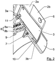
- figure 2 shows an enlarged and partially sectioned view of the digital camera (1) in the area of the mounted bracket (3).
- a section of the interior of the housing is shown in the left-hand area of the figure.
- a web (7) protrudes, which has a support profile for a filter.
- the circuit board stack (8) is arranged above it, which in the embodiment shown has two circuit boards connected to one another, which are designed as a main circuit board (8a) and as a sensor circuit board (8b).
- the sensor circuit board (8b) carries an image sensor (9) on its side shown below.
- the clip (3) is provided with material bends in its end regions.
- the bending area (3b) shown at the bottom right is used for a first hanging behind an associated profile (10) of the lower housing part (2b).
- the inside figure 2 A further bent area (3a) which can be seen at the top left of the clamp (3) is used for clipping into a counter-profile (11) of the housing upper part (2a).
- the perspective view in figure 3 shows the structure of the clip (3), which has a slightly angled bend (3c) in the direction of its longitudinal extent.
- the bend (3c) runs approximately in an area of the transition from the lower housing part (2b) to the upper housing part (2a).
- the bend (3c) supports an elastic elongation of the clip (3) when it is clipped in.
- the bent area (3a) associated with the housing upper part (2a) forms an undercut with the counter-profile (11) of the housing upper part (2a) in an assembled state.
- the bent area (3b) associated with the lower housing part (2b) is designed as a two-part spring element. The division into two enables an adaptation to the round outer contour of the lens mount (5) in the area of the profile (10).
- the clip (3) has two assembly aids (3d), which are implemented as recesses in the clip (3).
- the assembly process can be carried out in a very short time.
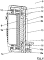
- FIG 4 shows a cross section of the circuit board stack (8).
- the circuit board stack (8) has two circuit boards, which are designed as a main circuit board (8a) and as a sensor circuit board (8b).
- electronic components (12) are arranged both on the sensor circuit board (8b) and on the main circuit board (8a), for example as capacitors, resistors, diodes and/or ICs can be trained.
- the main circuit board (8a) also carries the control element of the digital camera (1), which is designed as a main chip (13) and is implemented as an ASIC in the example shown.
- the sensor board (8b) has its in the figure 4 a contour milling (14) on the top and bottom sides, via which the position of the image sensor (9) in the digital camera (1) can be influenced. Furthermore, the sensor circuit board (8b) has two indentations (15) which are implemented as deep millings and which form pockets between the main circuit board (8a) and the sensor circuit board (8b) which serve to accommodate components (12) between the circuit boards.
- Electromagnetic shielding of the components (12) accommodated within a pocket formed in this way can be achieved by metallization in the region of the surfaces of the circuit boards delimiting the depressions (15).
- a connection device for an interface (16) is arranged on the main circuit board (8a), which has a fastening element (16a) and an I/O connector (16b).
- figure 5 shows in a cross-sectional representation of the digital camera (1) the use of contour milling (14) in the area of circuit boards in order to be able to carry out a height adjustment.
- the use of the clamps (3) for connecting the lower housing part (2b) and the upper housing part (2a) can also be seen in this cross-sectional view.
- the thickness (S) of the image sensor (9) is variable for different image sensors (9) that can be used in a digital camera (1) according to the invention, but is given in each individual case.
- a rough adjustment can be made by selecting the sensor circuit board (8b), which has a thickness (D) corresponding to the selection.
- the height (H) can be further adjusted by the adhesive used when assembling the circuit board stack (8) in the camera housing (2).
- the adhesive is applied to an assigned support (17) in the housing interior and/or the sensor circuit board (8b) in the area of the contour milling (14) and the sensor circuit board (8b) is aligned in the camera housing (2).
- the adhesive is then hardened and connects the sensor circuit board (8a) to the camera housing (2) in the area of the support (17).
- this possibility is only possible in a very limited range due to the shrinkage of the adhesive during curing and a temperature-dependent expansion of the adhesive after curing.
- an expansion board (18) which carries an additional electronic chip (19), e.g. designed as an FPGA, and a memory element (20), e.g. in the form of at least one RAM module, and which is connected via connecting plugs (21). the main circuit board (8a) can be connected.
- an additional electronic chip (19) e.g. designed as an FPGA
- a memory element (20) e.g. in the form of at least one RAM module, and which is connected via connecting plugs (21).
- the main circuit board (8a) can be connected.
- figure 6 illustrated in addition to figure 5 again the arrangement of the thickness (D) of the sensor board (8b) and the thickness (S) of the image sensor (9) and the depth (T) of the contour milling (14).
- Shown is a side view of a board stack (8) according to the invention, having a main board (8a) and a sensor board (8b).
- figure 7 illustrates in a perspective view the arrangement of an image sensor (9) on a sensor circuit board (8b) of a circuit board stack (8) according to the invention of a digital camera (1).
- a large number of electronic components (12) can be seen, which are arranged on the sensor circuit board (8b).
- a fastening element (16a) is arranged in the area of the main circuit board (8a), with which the mechanical securing of two connection devices of two interfaces (16) can be implemented.
- a two-part or multi-part design of the fastening element (16a) with an assignment of one part to at least one interface (16) can be implemented.
- a flash memory, a blocking capacitor, a voltage regulator, a power supply, a clock generator and/or a protective circuit can be used as associated electronic components (12).
- the corresponding components can also be used in multiple embodiments.
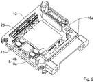
- a connector (23) and two external connecting devices (16) with a fastening element (16a) are arranged on the main board (8a) of the board stack (8) next to the main chip (13) and the other electronic components (12).
- the connector (23) serves as a connection option for an optional extension board (18), as shown in figure 5 shown.
- connection devices of the interfaces (16) each have an electrical connection device (16b) which implements the actual socket contact and which is electrically connected at least to the main circuit board (8a).
- a socket can be, for example, a USB, a CSI-2 or a Realize I/O interface.
- the associated fastening element (16a) is arranged in the area of an electrical connection device (16b) and is fastened to the main circuit board (8b) and/or the circuit board stack (8) by soldering and/or a mechanical connection, for example.
- a fastening element (16a) is advantageously made of a solid material, for example cast zinc, and has at least one mechanical connecting device (16c), which is designed, for example, as a screw thread.
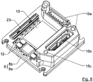
- This in figure 8 illustrated one-piece fastener (16a) is arranged in a 90 ° orientation to the main circuit board (8a).
- FIG 9 is an embodiment of the circuit board stack (8) of a digital camera (1) having a one-piece fastening element (16a) in a regional 90° orientation and a regional 180° orientation.
- figure 10 shows a perspective representation of the arrangement of a contour milling (14) of depth (T) in the area of the sensor circuit board (8b) and the arrangement of a small image sensor (9) on the sensor circuit board (8b).
- the image sensor (9) has an active surface (F).
- the thickness (D) of the sensor circuit board (8b) used is usually adapted to the image sensor (9) used.
- the image sensor (9) is usually covered with a glass plate (not shown).
- circuit board stack (8) makes it possible to implement a digital camera (1) with a very compact design. In particular, it is possible to minimize blocking capacitors that may be required due to the good connection of the main circuit board (8a) and the sensor circuit board (8b). In particular, direct soldering of the circuit boards can be carried out to avoid plug connectors. The exact positioning of the circuit boards on top of each other takes place automatically during soldering due to the surface tension of the liquid solder that connects the corresponding soldering pads on the circuit boards.
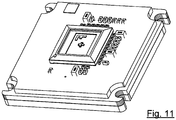
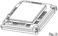
- figure 11 and figure 12 show the circuit board arrangement with image sensors (9) in different dimensions.
- FIG 13 shows a view of the underside of a sensor circuit board (8b) designed according to the invention.
- the sensor circuit board (8b) has two indentations (15) that accommodate two pockets form components (12) arranged on another circuit board. One of the pockets is divided into three sub-pockets. In the area of the unmilled structure, the sensor circuit board (8b) has a large number of soldering pads (25), which are used for contacting the circuit board to be connected.
- two holes are arranged in the area of the depressions (15), which serve as ventilation ducts for the space defined between the circuit board stack (8), camera housing (2) and filter or cover glass and enable pressure equalization. Without the possibility of pressure compensation, the optics can otherwise fog up from the inside if the ambient pressure changes.
- the structure formed by the soldered connections between the circuit boards of the circuit board stack (8) acts as a filter in the sense of a labyrinth for inflowing air and thus prevents the introduction of foreign bodies, such as dust, into the area of the image sensor (9).
- the flow chart in figure 14 illustrates the manufacturing process for the motherboard.
- a soldering paste is applied to the top of the circuit board. This is preferably lead-free.
- the application also preferably takes place in a printing process, similar to screen printing using a stencil. The thickness of the stencil determines the amount of solder paste applied.
- a first melting process is carried out (1st soldering process). This is followed by an automated optical inspection of the upper side. After rotating the board, solder paste is applied to the underside of the main board and then the intended components are positioned in the underside area. A melting process (2nd soldering process) is then carried out again and an automated optical inspection of the underside takes place again. After the optical inspection has been carried out, the individual boards are separated and the boards that have been separated from one another are placed in assigned trays. A test is then carried out with regard to the connections achieved and finally a function test.
- FIG 15 illustrates the manufacturing process for the sensor board.
- the soldering paste is first applied to the underside of the sensor board and a first melting process is carried out.
- the circuit board is then rotated and the soldering paste is applied to the top of the sensor circuit board.
- the intended electronic components are then positioned on the underside.
- the sensor is not yet positioned.
- the melting process is then carried out and also in this case Finally, an automated optical inspection of the underside takes place. Thereafter, the circuit boards are separated from one another and arranged separately from one another in trays.
- Solder paste usually contains solder and a flux.
- figure 16 illustrates the manufacturing process for combining the boards.
- An initially empty tray is provided with the main board and then the sensor board is added. Then the solder paste is applied to the underside of the sensor board.
- the sensor board is positioned on the main board and the sensor is added. Then the flux is placed on the underside of the sensor and the sensor is positioned on the sensor board. This is followed by a melting process for the sensor and finally a function test.
- electronic components are integrated in recesses within the circuit board stack in order to thereby support a compact structural realization.
- a height compensation takes place, in particular in relation to the image sensor, by means of at least one contour milling in the area of at least one circuit board.
- connection devices of interfaces is integrated into one or more fastening elements connected to the circuit board stack, and according to a further variant, a special soldering process is carried out to prevent damage to electronic components by the soldering process.
- housing parts are connected to each other through the use of at least one special spring clip to enable both a reliable connection of the housing components and a simple production flow.
- a corresponding data bus is preferably used.
- the definition of the individual camera functions and the envisaged coordination of the functions are preferably implemented via a main chip designed as an ASIC.
Landscapes
- Engineering & Computer Science (AREA)
- Multimedia (AREA)
- Signal Processing (AREA)
- Microelectronics & Electronic Packaging (AREA)
- Camera Bodies And Camera Details Or Accessories (AREA)
- Studio Devices (AREA)
- Cameras Adapted For Combination With Other Photographic Or Optical Apparatuses (AREA)
Applications Claiming Priority (2)
| Application Number | Priority Date | Filing Date | Title |
|---|---|---|---|
| DE102017004139 | 2017-04-27 | ||
| PCT/DE2018/000129 WO2018196900A1 (de) | 2017-04-27 | 2018-04-26 | Vorrichtung zur erfassung von daten |
Publications (2)
| Publication Number | Publication Date |
|---|---|
| EP3616397A1 EP3616397A1 (de) | 2020-03-04 |
| EP3616397B1 true EP3616397B1 (de) | 2022-01-12 |
Family
ID=62455282
Family Applications (1)
| Application Number | Title | Priority Date | Filing Date |
|---|---|---|---|
| EP18728012.8A Active EP3616397B1 (de) | 2017-04-27 | 2018-04-26 | Vorrichtung zur erfassung von daten |
Country Status (7)
| Country | Link |
|---|---|
| US (1) | US11838613B2 (es) |
| EP (1) | EP3616397B1 (es) |
| JP (1) | JP7291630B2 (es) |
| CN (1) | CN110521200A (es) |
| DE (2) | DE112018002209A5 (es) |
| ES (1) | ES2911193T3 (es) |
| WO (1) | WO2018196900A1 (es) |
Citations (2)
| Publication number | Priority date | Publication date | Assignee | Title |
|---|---|---|---|---|
| JP2005079408A (ja) * | 2003-09-01 | 2005-03-24 | Olympus Corp | 小型高密度実装モジュール及びその製造方法 |
| US20070007636A1 (en) * | 2005-06-30 | 2007-01-11 | Samsung Electro-Mechanics Co., Ltd. | Parallel chip embedded printed circuit board and manufacturing method thereof |
Family Cites Families (43)
| Publication number | Priority date | Publication date | Assignee | Title |
|---|---|---|---|---|
| US5221964A (en) | 1991-08-05 | 1993-06-22 | Dalsa Inc | Electronically expandable modular ccd camera |
| JP2002076314A (ja) * | 2000-08-30 | 2002-03-15 | Texas Instr Japan Ltd | 超小型撮像装置 |
| US20040121503A1 (en) | 2002-12-19 | 2004-06-24 | Albert Ferland | Image sensor positioning system and method |
| DE10328265A1 (de) | 2003-06-23 | 2005-01-27 | Infineon Technologies Ag | Sensorbauteil und Nutzen zu seiner Herstellung |
| TWI220307B (en) * | 2003-10-15 | 2004-08-11 | Benq Corp | Thermal enhanced package structure and its formation method |
| US7217045B2 (en) | 2005-01-03 | 2007-05-15 | Robert Bosch Gmbh | Connect/disconnect mechanism for a surveillance camera head |
| DE102005027892A1 (de) | 2005-06-16 | 2006-12-28 | Basler Ag | Verfahren zum genauen Ausrichten eines lichtempfindlichen Sensors in einem Kameragehäuse sowie Kameragehäuse |
| JP4589183B2 (ja) * | 2005-06-29 | 2010-12-01 | 株式会社Suwaオプトロニクス | 撮像装置および撮像システム |
| JP5111937B2 (ja) * | 2007-05-23 | 2013-01-09 | 京セラ株式会社 | 携帯電子機器 |
| US20090079863A1 (en) * | 2007-09-20 | 2009-03-26 | Susumu Aoki | Camera module, manufacturing method of imaging apparatus and hot melt molding method |
| KR100997343B1 (ko) * | 2008-07-29 | 2010-11-29 | 주식회사 동부하이텍 | 이미지센서 및 그 제조방법 |
| KR100915134B1 (ko) * | 2008-12-10 | 2009-09-03 | 옵토팩 주식회사 | 이미지 센서 카메라 모듈 및 그 제조 방법 |
| KR101070058B1 (ko) * | 2008-12-24 | 2011-10-04 | 삼성전기주식회사 | 카메라 모듈 패키지 |
| US9473681B2 (en) * | 2011-06-10 | 2016-10-18 | Flir Systems, Inc. | Infrared camera system housing with metalized surface |
| EP3438721B1 (en) * | 2009-03-25 | 2020-07-08 | Magna Electronics Inc. | Vehicular camera and lens assembly |
| US8623753B1 (en) * | 2009-05-28 | 2014-01-07 | Amkor Technology, Inc. | Stackable protruding via package and method |
| TWI561884B (en) * | 2010-04-06 | 2016-12-11 | Hon Hai Prec Ind Co Ltd | Camera module and method for making same |
| JP5565117B2 (ja) * | 2010-06-07 | 2014-08-06 | 株式会社リコー | 撮像装置 |
| US8308379B2 (en) * | 2010-12-01 | 2012-11-13 | Digitaloptics Corporation | Three-pole tilt control system for camera module |
| FR2968432B1 (fr) * | 2010-12-06 | 2012-12-28 | Oberthur Technologies | Procédé d'encartage d'un module dans une carte a microcircuit |
| JP5853389B2 (ja) * | 2011-03-28 | 2016-02-09 | ソニー株式会社 | 半導体装置及び半導体装置の製造方法。 |
| US10389953B2 (en) * | 2011-06-10 | 2019-08-20 | Flir Systems, Inc. | Infrared imaging device having a shutter |
| JP2013115289A (ja) * | 2011-11-30 | 2013-06-10 | Sony Corp | 半導体装置、半導体装置の製造方法、および電子機器 |
| WO2013118501A1 (ja) * | 2012-02-07 | 2013-08-15 | 株式会社ニコン | 撮像ユニットおよび撮像装置 |
| GB2502947A (en) * | 2012-04-17 | 2013-12-18 | St Microelectronics Res & Dev | Camera module with bridge-mounted image sensor located in substrate cavity |
| US20150001533A1 (en) * | 2013-06-28 | 2015-01-01 | Semiconductor Energy Laboratory Co., Ltd. | Semiconductor device |
| CN105452918B (zh) * | 2013-07-05 | 2019-02-05 | 古河电气工业株式会社 | 光模块、光模块的安装方法、光模块搭载电路基板、光模块评价仪器系统、电路基板以及通信系统 |
| WO2015015986A1 (ja) * | 2013-08-01 | 2015-02-05 | 富士フイルム株式会社 | 撮像モジュール、及びこれを備えた電子機器、並びに撮像モジュールの製造方法 |
| US9521754B1 (en) | 2013-08-19 | 2016-12-13 | Multek Technologies Limited | Embedded components in a substrate |
| CN104681510A (zh) * | 2013-12-03 | 2015-06-03 | 晟碟信息科技(上海)有限公司 | 用于嵌入半导体裸片的桥结构 |
| CN104752380B (zh) * | 2013-12-31 | 2018-10-09 | 晟碟信息科技(上海)有限公司 | 半导体装置 |
| US20170080255A1 (en) * | 2014-03-15 | 2017-03-23 | Cerevast Medical Inc. | Thin and wearable ultrasound phased array devices |
| US9607964B2 (en) * | 2014-03-28 | 2017-03-28 | Intel Corporation | Method and materials for warpage thermal and interconnect solutions |
| CN204316686U (zh) * | 2014-11-28 | 2015-05-06 | 歌尔声学股份有限公司 | 一种电路板外壳和一种麦克风单体 |
| US9997554B2 (en) * | 2014-12-24 | 2018-06-12 | Stmicroelectronics Pte Ltd | Chip scale package camera module with glass interposer having lateral conductive traces between a first and second glass layer and method for making the same |
| US10070088B2 (en) * | 2015-01-05 | 2018-09-04 | Canon Kabushiki Kaisha | Image sensor and image capturing apparatus for simultaneously performing focus detection and image generation |
| CN204836357U (zh) * | 2015-08-31 | 2015-12-02 | 成都动力视讯科技股份有限公司 | 图像传感器电路板平整装置及系统 |
| KR102458297B1 (ko) * | 2016-01-12 | 2022-10-25 | 삼성전자주식회사 | 전자 장치 및 그를 제조하는 방법 |
| US10660204B2 (en) * | 2016-04-14 | 2020-05-19 | Lg Innotek Co., Ltd. | Device for fixing camera module circuit board, and camera module |
| US10602039B2 (en) * | 2016-09-19 | 2020-03-24 | Microsoft Technology Licensing, Llc | Ultra-compact image sensor assembly for thin profile devices |
| US9888197B1 (en) * | 2017-01-04 | 2018-02-06 | Semiconductor Components Industries, Llc | Methods and apparatus for a CMOS image sensor with an in-pixel amplifier |
| US10306114B2 (en) * | 2017-02-10 | 2019-05-28 | Google Llc | Camera module mounting in an electronic device |
| JP7126167B2 (ja) * | 2019-03-28 | 2022-08-26 | パナソニックIpマネジメント株式会社 | はんだペーストおよび実装構造体 |
-
2018
- 2018-04-26 DE DE112018002209.9T patent/DE112018002209A5/de active Pending
- 2018-04-26 JP JP2019555674A patent/JP7291630B2/ja active Active
- 2018-04-26 DE DE102018003729.1A patent/DE102018003729A1/de not_active Withdrawn
- 2018-04-26 ES ES18728012T patent/ES2911193T3/es active Active
- 2018-04-26 CN CN201880025369.4A patent/CN110521200A/zh active Pending
- 2018-04-26 US US16/607,597 patent/US11838613B2/en active Active
- 2018-04-26 EP EP18728012.8A patent/EP3616397B1/de active Active
- 2018-04-26 WO PCT/DE2018/000129 patent/WO2018196900A1/de unknown
Patent Citations (2)
| Publication number | Priority date | Publication date | Assignee | Title |
|---|---|---|---|---|
| JP2005079408A (ja) * | 2003-09-01 | 2005-03-24 | Olympus Corp | 小型高密度実装モジュール及びその製造方法 |
| US20070007636A1 (en) * | 2005-06-30 | 2007-01-11 | Samsung Electro-Mechanics Co., Ltd. | Parallel chip embedded printed circuit board and manufacturing method thereof |
Also Published As
| Publication number | Publication date |
|---|---|
| JP7291630B2 (ja) | 2023-06-15 |
| JP2020520569A (ja) | 2020-07-09 |
| DE112018002209A5 (de) | 2020-05-07 |
| ES2911193T3 (es) | 2022-05-18 |
| CN110521200A (zh) | 2019-11-29 |
| US11838613B2 (en) | 2023-12-05 |
| DE102018003729A1 (de) | 2018-10-31 |
| WO2018196900A1 (de) | 2018-11-01 |
| US20210289109A1 (en) | 2021-09-16 |
| EP3616397A1 (de) | 2020-03-04 |
Similar Documents
| Publication | Publication Date | Title |
|---|---|---|
| DE602004003612T2 (de) | Kompaktes Kameramodul | |
| DE10344768B3 (de) | Optisches Modul mit federndem Element zwischen Linsenhalter und Schaltungsträger und optisches System | |
| EP0712265B1 (de) | Baugruppe | |
| DE102007057172B4 (de) | Stereokamera zur Umgebungserfassung | |
| EP3280127A1 (de) | Kamerasystem | |
| DE102007008109B4 (de) | Trägerplattenanordnung | |
| DE10122929A1 (de) | Festkörper-Abbildungsvorrichtung | |
| DE102011050895A1 (de) | Mikrosensor | |
| DE202008018126U1 (de) | Lötanschlusselement | |
| DE112019000620T5 (de) | Elektronische schaltung | |
| DE102016205938A1 (de) | Elektronische Vorrichtung | |
| WO2016124184A1 (de) | Kameramodul sowie verfahren zur herstellung | |
| DE10344767B4 (de) | Optisches Modul und optisches System | |
| DE102015225794B4 (de) | Justageelement für ein Kameramodul, Justagevorrichtung und Verfahren zur Einstellung eines axialen Abstandes | |
| DE3627372A1 (de) | Kuehlkoerper fuer elektronische bauelemente | |
| EP3616397B1 (de) | Vorrichtung zur erfassung von daten | |
| EP3477781A1 (de) | Steckerbuchse für leiterplatinen | |
| DE102017217317A1 (de) | Kameramodul mit Kompensationselement | |
| DE102014114569A1 (de) | Kamera für ein Kraftfahrzeug mit einer Haltevorrichtung | |
| DE102014207148A1 (de) | Antennenplatine für die Oberflächenmontage | |
| DE102017210379A1 (de) | Bildsensormodul | |
| DE102009056658B4 (de) | Objektiv für eine Halbleiterkamera und Verfahren zum Fokussieren einer Halbleiterkamera | |
| EP1771883B1 (de) | Image-modul | |
| DE102016223786A1 (de) | Oberflächenmontiertes Befestigungselement | |
| EP3056881B1 (de) | Passiv-infrarot-bewegungsmelder |
Legal Events
| Date | Code | Title | Description |
|---|---|---|---|
| STAA | Information on the status of an ep patent application or granted ep patent |
Free format text: STATUS: UNKNOWN |
|
| STAA | Information on the status of an ep patent application or granted ep patent |
Free format text: STATUS: THE INTERNATIONAL PUBLICATION HAS BEEN MADE |
|
| PUAI | Public reference made under article 153(3) epc to a published international application that has entered the european phase |
Free format text: ORIGINAL CODE: 0009012 |
|
| STAA | Information on the status of an ep patent application or granted ep patent |
Free format text: STATUS: REQUEST FOR EXAMINATION WAS MADE |
|
| 17P | Request for examination filed |
Effective date: 20190819 |
|
| AK | Designated contracting states |
Kind code of ref document: A1 Designated state(s): AL AT BE BG CH CY CZ DE DK EE ES FI FR GB GR HR HU IE IS IT LI LT LU LV MC MK MT NL NO PL PT RO RS SE SI SK SM TR |
|
| AX | Request for extension of the european patent |
Extension state: BA ME |
|
| DAV | Request for validation of the european patent (deleted) | ||
| DAX | Request for extension of the european patent (deleted) | ||
| STAA | Information on the status of an ep patent application or granted ep patent |
Free format text: STATUS: EXAMINATION IS IN PROGRESS |
|
| 17Q | First examination report despatched |
Effective date: 20210312 |
|
| GRAP | Despatch of communication of intention to grant a patent |
Free format text: ORIGINAL CODE: EPIDOSNIGR1 |
|
| STAA | Information on the status of an ep patent application or granted ep patent |
Free format text: STATUS: GRANT OF PATENT IS INTENDED |
|
| INTG | Intention to grant announced |
Effective date: 20210916 |
|
| GRAS | Grant fee paid |
Free format text: ORIGINAL CODE: EPIDOSNIGR3 |
|
| GRAA | (expected) grant |
Free format text: ORIGINAL CODE: 0009210 |
|
| STAA | Information on the status of an ep patent application or granted ep patent |
Free format text: STATUS: THE PATENT HAS BEEN GRANTED |
|
| AK | Designated contracting states |
Kind code of ref document: B1 Designated state(s): AL AT BE BG CH CY CZ DE DK EE ES FI FR GB GR HR HU IE IS IT LI LT LU LV MC MK MT NL NO PL PT RO RS SE SI SK SM TR |
|
| REG | Reference to a national code |
Ref country code: GB Ref legal event code: FG4D Free format text: NOT ENGLISH |
|
| REG | Reference to a national code |
Ref country code: CH Ref legal event code: EP |
|
| REG | Reference to a national code |
Ref country code: DE Ref legal event code: R096 Ref document number: 502018008512 Country of ref document: DE |
|
| REG | Reference to a national code |
Ref country code: IE Ref legal event code: FG4D Free format text: LANGUAGE OF EP DOCUMENT: GERMAN |
|
| REG | Reference to a national code |
Ref country code: AT Ref legal event code: REF Ref document number: 1463142 Country of ref document: AT Kind code of ref document: T Effective date: 20220215 |
|
| REG | Reference to a national code |
Ref country code: NL Ref legal event code: FP |
|
| REG | Reference to a national code |
Ref country code: LT Ref legal event code: MG9D |
|
| REG | Reference to a national code |
Ref country code: ES Ref legal event code: FG2A Ref document number: 2911193 Country of ref document: ES Kind code of ref document: T3 Effective date: 20220518 |
|
| PG25 | Lapsed in a contracting state [announced via postgrant information from national office to epo] |
Ref country code: SE Free format text: LAPSE BECAUSE OF FAILURE TO SUBMIT A TRANSLATION OF THE DESCRIPTION OR TO PAY THE FEE WITHIN THE PRESCRIBED TIME-LIMIT Effective date: 20220112 Ref country code: RS Free format text: LAPSE BECAUSE OF FAILURE TO SUBMIT A TRANSLATION OF THE DESCRIPTION OR TO PAY THE FEE WITHIN THE PRESCRIBED TIME-LIMIT Effective date: 20220112 Ref country code: PT Free format text: LAPSE BECAUSE OF FAILURE TO SUBMIT A TRANSLATION OF THE DESCRIPTION OR TO PAY THE FEE WITHIN THE PRESCRIBED TIME-LIMIT Effective date: 20220512 Ref country code: NO Free format text: LAPSE BECAUSE OF FAILURE TO SUBMIT A TRANSLATION OF THE DESCRIPTION OR TO PAY THE FEE WITHIN THE PRESCRIBED TIME-LIMIT Effective date: 20220412 Ref country code: LT Free format text: LAPSE BECAUSE OF FAILURE TO SUBMIT A TRANSLATION OF THE DESCRIPTION OR TO PAY THE FEE WITHIN THE PRESCRIBED TIME-LIMIT Effective date: 20220112 Ref country code: HR Free format text: LAPSE BECAUSE OF FAILURE TO SUBMIT A TRANSLATION OF THE DESCRIPTION OR TO PAY THE FEE WITHIN THE PRESCRIBED TIME-LIMIT Effective date: 20220112 Ref country code: BG Free format text: LAPSE BECAUSE OF FAILURE TO SUBMIT A TRANSLATION OF THE DESCRIPTION OR TO PAY THE FEE WITHIN THE PRESCRIBED TIME-LIMIT Effective date: 20220412 |
|
| PG25 | Lapsed in a contracting state [announced via postgrant information from national office to epo] |
Ref country code: PL Free format text: LAPSE BECAUSE OF FAILURE TO SUBMIT A TRANSLATION OF THE DESCRIPTION OR TO PAY THE FEE WITHIN THE PRESCRIBED TIME-LIMIT Effective date: 20220112 Ref country code: LV Free format text: LAPSE BECAUSE OF FAILURE TO SUBMIT A TRANSLATION OF THE DESCRIPTION OR TO PAY THE FEE WITHIN THE PRESCRIBED TIME-LIMIT Effective date: 20220112 Ref country code: GR Free format text: LAPSE BECAUSE OF FAILURE TO SUBMIT A TRANSLATION OF THE DESCRIPTION OR TO PAY THE FEE WITHIN THE PRESCRIBED TIME-LIMIT Effective date: 20220413 Ref country code: FI Free format text: LAPSE BECAUSE OF FAILURE TO SUBMIT A TRANSLATION OF THE DESCRIPTION OR TO PAY THE FEE WITHIN THE PRESCRIBED TIME-LIMIT Effective date: 20220112 |
|
| PG25 | Lapsed in a contracting state [announced via postgrant information from national office to epo] |
Ref country code: IS Free format text: LAPSE BECAUSE OF FAILURE TO SUBMIT A TRANSLATION OF THE DESCRIPTION OR TO PAY THE FEE WITHIN THE PRESCRIBED TIME-LIMIT Effective date: 20220512 |
|
| REG | Reference to a national code |
Ref country code: DE Ref legal event code: R097 Ref document number: 502018008512 Country of ref document: DE |
|
| PG25 | Lapsed in a contracting state [announced via postgrant information from national office to epo] |
Ref country code: SM Free format text: LAPSE BECAUSE OF FAILURE TO SUBMIT A TRANSLATION OF THE DESCRIPTION OR TO PAY THE FEE WITHIN THE PRESCRIBED TIME-LIMIT Effective date: 20220112 Ref country code: SK Free format text: LAPSE BECAUSE OF FAILURE TO SUBMIT A TRANSLATION OF THE DESCRIPTION OR TO PAY THE FEE WITHIN THE PRESCRIBED TIME-LIMIT Effective date: 20220112 Ref country code: RO Free format text: LAPSE BECAUSE OF FAILURE TO SUBMIT A TRANSLATION OF THE DESCRIPTION OR TO PAY THE FEE WITHIN THE PRESCRIBED TIME-LIMIT Effective date: 20220112 Ref country code: EE Free format text: LAPSE BECAUSE OF FAILURE TO SUBMIT A TRANSLATION OF THE DESCRIPTION OR TO PAY THE FEE WITHIN THE PRESCRIBED TIME-LIMIT Effective date: 20220112 Ref country code: DK Free format text: LAPSE BECAUSE OF FAILURE TO SUBMIT A TRANSLATION OF THE DESCRIPTION OR TO PAY THE FEE WITHIN THE PRESCRIBED TIME-LIMIT Effective date: 20220112 Ref country code: CZ Free format text: LAPSE BECAUSE OF FAILURE TO SUBMIT A TRANSLATION OF THE DESCRIPTION OR TO PAY THE FEE WITHIN THE PRESCRIBED TIME-LIMIT Effective date: 20220112 |
|
| PLBE | No opposition filed within time limit |
Free format text: ORIGINAL CODE: 0009261 |
|
| STAA | Information on the status of an ep patent application or granted ep patent |
Free format text: STATUS: NO OPPOSITION FILED WITHIN TIME LIMIT |
|
| REG | Reference to a national code |
Ref country code: DE Ref legal event code: R079 Ref document number: 502018008512 Country of ref document: DE Free format text: PREVIOUS MAIN CLASS: H04N0005225000 Ipc: H04N0023000000 |
|
| PG25 | Lapsed in a contracting state [announced via postgrant information from national office to epo] |
Ref country code: AL Free format text: LAPSE BECAUSE OF FAILURE TO SUBMIT A TRANSLATION OF THE DESCRIPTION OR TO PAY THE FEE WITHIN THE PRESCRIBED TIME-LIMIT Effective date: 20220112 |
|
| 26N | No opposition filed |
Effective date: 20221013 |
|
| PG25 | Lapsed in a contracting state [announced via postgrant information from national office to epo] |
Ref country code: MC Free format text: LAPSE BECAUSE OF FAILURE TO SUBMIT A TRANSLATION OF THE DESCRIPTION OR TO PAY THE FEE WITHIN THE PRESCRIBED TIME-LIMIT Effective date: 20220112 Ref country code: LU Free format text: LAPSE BECAUSE OF NON-PAYMENT OF DUE FEES Effective date: 20220426 |
|
| PG25 | Lapsed in a contracting state [announced via postgrant information from national office to epo] |
Ref country code: SI Free format text: LAPSE BECAUSE OF FAILURE TO SUBMIT A TRANSLATION OF THE DESCRIPTION OR TO PAY THE FEE WITHIN THE PRESCRIBED TIME-LIMIT Effective date: 20220112 |
|
| PG25 | Lapsed in a contracting state [announced via postgrant information from national office to epo] |
Ref country code: IE Free format text: LAPSE BECAUSE OF NON-PAYMENT OF DUE FEES Effective date: 20220426 |
|
| PGFP | Annual fee paid to national office [announced via postgrant information from national office to epo] |
Ref country code: IT Payment date: 20230426 Year of fee payment: 6 Ref country code: FR Payment date: 20230424 Year of fee payment: 6 Ref country code: ES Payment date: 20230627 Year of fee payment: 6 Ref country code: DE Payment date: 20230420 Year of fee payment: 6 Ref country code: CH Payment date: 20230502 Year of fee payment: 6 |
|
| PGFP | Annual fee paid to national office [announced via postgrant information from national office to epo] |
Ref country code: TR Payment date: 20230424 Year of fee payment: 6 Ref country code: AT Payment date: 20230420 Year of fee payment: 6 |
|
| PGFP | Annual fee paid to national office [announced via postgrant information from national office to epo] |
Ref country code: BE Payment date: 20230419 Year of fee payment: 6 |
|
| PGFP | Annual fee paid to national office [announced via postgrant information from national office to epo] |
Ref country code: GB Payment date: 20230419 Year of fee payment: 6 |
|
| PG25 | Lapsed in a contracting state [announced via postgrant information from national office to epo] |
Ref country code: MK Free format text: LAPSE BECAUSE OF FAILURE TO SUBMIT A TRANSLATION OF THE DESCRIPTION OR TO PAY THE FEE WITHIN THE PRESCRIBED TIME-LIMIT Effective date: 20220112 Ref country code: CY Free format text: LAPSE BECAUSE OF FAILURE TO SUBMIT A TRANSLATION OF THE DESCRIPTION OR TO PAY THE FEE WITHIN THE PRESCRIBED TIME-LIMIT Effective date: 20220112 |
|
| PGFP | Annual fee paid to national office [announced via postgrant information from national office to epo] |
Ref country code: NL Payment date: 20240418 Year of fee payment: 7 |