EP3602640B1 - Nanodrahtstruktur und verfahren zu ihrer herstellung - Google Patents
Nanodrahtstruktur und verfahren zu ihrer herstellung Download PDFInfo
- Publication number
- EP3602640B1 EP3602640B1 EP18711346.9A EP18711346A EP3602640B1 EP 3602640 B1 EP3602640 B1 EP 3602640B1 EP 18711346 A EP18711346 A EP 18711346A EP 3602640 B1 EP3602640 B1 EP 3602640B1
- Authority
- EP
- European Patent Office
- Prior art keywords
- nanowires
- membrane
- layer
- receiving ends
- nanowire
- Prior art date
- Legal status (The legal status is an assumption and is not a legal conclusion. Google has not performed a legal analysis and makes no representation as to the accuracy of the status listed.)
- Active
Links
Images

Classifications
-
- H—ELECTRICITY
- H10—SEMICONDUCTOR DEVICES; ELECTRIC SOLID-STATE DEVICES NOT OTHERWISE PROVIDED FOR
- H10H—INORGANIC LIGHT-EMITTING SEMICONDUCTOR DEVICES HAVING POTENTIAL BARRIERS
- H10H20/00—Individual inorganic light-emitting semiconductor devices having potential barriers, e.g. light-emitting diodes [LED]
- H10H20/80—Constructional details
- H10H20/83—Electrodes
- H10H20/832—Electrodes characterised by their material
- H10H20/833—Transparent materials
-
- H—ELECTRICITY
- H10—SEMICONDUCTOR DEVICES; ELECTRIC SOLID-STATE DEVICES NOT OTHERWISE PROVIDED FOR
- H10H—INORGANIC LIGHT-EMITTING SEMICONDUCTOR DEVICES HAVING POTENTIAL BARRIERS
- H10H20/00—Individual inorganic light-emitting semiconductor devices having potential barriers, e.g. light-emitting diodes [LED]
- H10H20/01—Manufacture or treatment
- H10H20/011—Manufacture or treatment of bodies, e.g. forming semiconductor layers
- H10H20/013—Manufacture or treatment of bodies, e.g. forming semiconductor layers having light-emitting regions comprising only Group III-V materials
- H10H20/0133—Manufacture or treatment of bodies, e.g. forming semiconductor layers having light-emitting regions comprising only Group III-V materials with a substrate not being Group III-V materials
- H10H20/01335—Manufacture or treatment of bodies, e.g. forming semiconductor layers having light-emitting regions comprising only Group III-V materials with a substrate not being Group III-V materials the light-emitting regions comprising nitride materials
-
- H—ELECTRICITY
- H10—SEMICONDUCTOR DEVICES; ELECTRIC SOLID-STATE DEVICES NOT OTHERWISE PROVIDED FOR
- H10H—INORGANIC LIGHT-EMITTING SEMICONDUCTOR DEVICES HAVING POTENTIAL BARRIERS
- H10H20/00—Individual inorganic light-emitting semiconductor devices having potential barriers, e.g. light-emitting diodes [LED]
- H10H20/01—Manufacture or treatment
- H10H20/011—Manufacture or treatment of bodies, e.g. forming semiconductor layers
- H10H20/018—Bonding of wafers
-
- H—ELECTRICITY
- H10—SEMICONDUCTOR DEVICES; ELECTRIC SOLID-STATE DEVICES NOT OTHERWISE PROVIDED FOR
- H10H—INORGANIC LIGHT-EMITTING SEMICONDUCTOR DEVICES HAVING POTENTIAL BARRIERS
- H10H20/00—Individual inorganic light-emitting semiconductor devices having potential barriers, e.g. light-emitting diodes [LED]
- H10H20/80—Constructional details
- H10H20/81—Bodies
- H10H20/813—Bodies having a plurality of light-emitting regions, e.g. multi-junction LEDs or light-emitting devices having photoluminescent regions within the bodies
-
- H—ELECTRICITY
- H10—SEMICONDUCTOR DEVICES; ELECTRIC SOLID-STATE DEVICES NOT OTHERWISE PROVIDED FOR
- H10H—INORGANIC LIGHT-EMITTING SEMICONDUCTOR DEVICES HAVING POTENTIAL BARRIERS
- H10H20/00—Individual inorganic light-emitting semiconductor devices having potential barriers, e.g. light-emitting diodes [LED]
- H10H20/80—Constructional details
- H10H20/81—Bodies
- H10H20/817—Bodies characterised by the crystal structures or orientations, e.g. polycrystalline, amorphous or porous
-
- H—ELECTRICITY
- H10—SEMICONDUCTOR DEVICES; ELECTRIC SOLID-STATE DEVICES NOT OTHERWISE PROVIDED FOR
- H10H—INORGANIC LIGHT-EMITTING SEMICONDUCTOR DEVICES HAVING POTENTIAL BARRIERS
- H10H20/00—Individual inorganic light-emitting semiconductor devices having potential barriers, e.g. light-emitting diodes [LED]
- H10H20/80—Constructional details
- H10H20/81—Bodies
- H10H20/822—Materials of the light-emitting regions
- H10H20/824—Materials of the light-emitting regions comprising only Group III-V materials, e.g. GaP
- H10H20/825—Materials of the light-emitting regions comprising only Group III-V materials, e.g. GaP containing nitrogen, e.g. GaN
-
- H—ELECTRICITY
- H10—SEMICONDUCTOR DEVICES; ELECTRIC SOLID-STATE DEVICES NOT OTHERWISE PROVIDED FOR
- H10H—INORGANIC LIGHT-EMITTING SEMICONDUCTOR DEVICES HAVING POTENTIAL BARRIERS
- H10H20/00—Individual inorganic light-emitting semiconductor devices having potential barriers, e.g. light-emitting diodes [LED]
- H10H20/80—Constructional details
- H10H20/81—Bodies
- H10H20/822—Materials of the light-emitting regions
- H10H20/826—Materials of the light-emitting regions comprising only Group IV materials
-
- H—ELECTRICITY
- H10—SEMICONDUCTOR DEVICES; ELECTRIC SOLID-STATE DEVICES NOT OTHERWISE PROVIDED FOR
- H10H—INORGANIC LIGHT-EMITTING SEMICONDUCTOR DEVICES HAVING POTENTIAL BARRIERS
- H10H20/00—Individual inorganic light-emitting semiconductor devices having potential barriers, e.g. light-emitting diodes [LED]
- H10H20/01—Manufacture or treatment
- H10H20/032—Manufacture or treatment of electrodes
Definitions
- the invention relates to a method for producing a nanowire structure.
- the invention also relates to a structure obtained by implementing the production method.
- the invention relates in particular to the field of light-emitting diodes (LEDs). These diodes can emit over an emission range extending from visible to ultraviolet. More precisely, the invention relates to the family of nanowire LEDs but can also be applied to other devices with nanostructures. In general, the invention relates to any LED or any device consisting of one, a few or a set of three-dimensional, non-coalesced nanostructures, deposited or etched on a substrate.
- LEDs light-emitting diodes
- the document KR 101 338 148 B1 discloses a method for producing a structure comprising a membrane of a first material in contact with receiving ends of a plurality of nanowires.
- the aim of the invention is to remedy the drawbacks cited above and to improve the methods for producing nanowire structures which must be electrically connected.
- the invention proposes a method making it possible to reliably produce structures with electrically connected nanowires.
- the method of producing a structure is defined by claim 1.
- the method may comprise a step of depositing a layer of a second electrically conductive material on the membrane, in particular a step of depositing a layer of a second material identical to the first material.
- the membrane may be transparent and electrically conductive and/or the membrane may be intended to form an electrode and/or the nanowires may be light-emitting diode structures.
- the structure is rinsed with a solvent so as to dissolve a layer of the membrane device, in particular so as to dissolve a layer of membrane device resin.
- the step of conforming the nanowire device can be implemented by molecular beam epitaxy or by metal-organic vapor phase epitaxy or by etching.
- the conformation step may include conforming the device so that it comprises a first substrate, the nanowires being arranged on the first substrate, in particular the nanowires being arranged perpendicularly or substantially perpendicularly on a surface of the first substrate, and/or so that the nanowires are prismatic or substantially prismatic and/or so that the nanowires have light-emitting diode structures.
- the shaping step may include shaping the receiving ends so that they form a planar or substantially planar discontinuous surface.
- the conformation step may include conforming the device so that the ratio of the sum of the areas of the surfaces of the receiving ends relative to the continuous area of the surface of a membrane intended to come into contact with the receiving ends either greater than 80% or greater than 90% or greater than 95%.
- the conformation step may include conforming nanowires such that the nanowires have a geometry that widens or flares toward the receiving ends and/or the conformation step may include conforming nanowires such that the nanowires constitute micro-pillars or nano-pillars including the receiving ends whose surfaces have dimensions greater than those of the diameters of the nanowires at a distance from the receiving end.
- the conforming step may include conforming nanowires such that they each include a body and a head, the head having a receiving end, the surface of the receiving end having an area 20% greater, or even 50% greater, than the area of a section of the body of a nanowire, in particular the area of a section of the nanowire measured parallel to the receiving end at at least 2 ⁇ m distance from the receiving end or to the area of a section of the nanowire measured parallel to the receiving end in the middle of the nanowire.
- the conformation step may comprise the conformation of the bodies of the nanowires into stacks of an n-type GaN layer, an InGa layer and a blocking layer.
- the conformation step may include the conformation of the heads of the nanowires into stacks of a p-type GaN layer and a p++-type GaN layer.
- the conformation step may include the conformation of the nanowires made of silicon-based material.
- a structure in particular a nanowire light-emitting diode, is obtained by implementing the production method defined above.
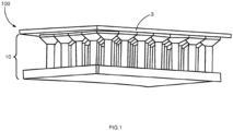
- nanowire light-emitting diode 100 One embodiment of a nanowire light-emitting diode 100 is described below with reference to the figure 1 .
- the diode includes a nanowire structure.
- the structure comprises a nanowire device 10 and a membrane 3 made of a first material, in particular indium-tin oxide.
- the nanowires have light-emitting diode structures.
- the membrane covers the nanowire device.
- the membrane covers in particular the ends of the nanowires, called receiving ends of the membrane or receiving ends.
- the nanowires are non-coalesced.
- the receiving ends form a discontinuous surface.
- discontinuous surface we mean for example that the receiving ends do not touch each other.
- at least certain receiving surfaces are arranged at a distance from others neighboring reception surfaces.
- each receiving surface is arranged at a distance from other neighboring receiving surfaces.
- the structure 100 may comprise a layer 4 of a second electrically conductive material, in particular a second material identical to the first material. This layer then covers the membrane 3 as shown in the Figure 9 .
- the membrane is electrically conductive. Indeed, it is intended to serve as an electrode for injecting current into the nanowires or as an electrode for applying a potential to the nanowires. In the case of a light-emitting diode structure, the membrane is advantageously transparent.
- the attached membrane must be thin enough and/or flexible enough to correctly match the surfaces of the receiving ends of the nanowires.
- the device 10 comprises at least one nanowire.
- the device 10 comprises a plurality of nanowires. These nanowires are, for example, distributed in a pattern, each at a distance from the others.
- the nanowires are non-coalesced.
- the receiving ends form a discontinuous surface.
- the nanowires are arranged on a substrate 2 in several successive rows.
- the nanowires can be arranged one behind the other in rows. Thus, lines of nanowires are oriented perpendicular to the rows of nanowires. Alternatively, the nanowires can be arranged in a staggered manner, with each nanowire in a subsequent row being placed between two nanowires of a previous row. Alternatively again, the nanowires can also be arranged more randomly.
- the nanowires have a geometry that widens or flares towards the receiving ends. More preferably, the nanowires constitute micro-pillars or nano-pillars including the receiving ends whose surfaces have dimensions greater than those of the diameters of the nanowires at a distance from the receiving end.
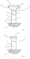
- nanowire preferably certain nanowires, more preferably all the nanowires, each comprise a body 11; 11' and a head 12; 12'.
- nanowire we preferably mean, throughout this document, any structure extending mainly in a direction A or along a curve and having a dimension transverse to this direction or this curve of the order of one micrometer or less than one micrometer. More preferably, all the dimensions of the structure measured transversely to direction A or to the curve are of the order of one micrometer or less than one micrometer.
- the nanowires are arranged perpendicularly or substantially perpendicularly on a surface 21 of the substrate 2.
- a direction A or a curve along which the nanowires extend at the surface 21 is perpendicular or substantially perpendicular to this surface 21.
- Surface 21 is a flat surface.
- the surface may be a non-planar ruled surface, or even a left surface.
- the nanowires are preferably prismatic or substantially prismatic, in particular in the shape of straight prisms.
- the nanowires can have a hexagonal section.
- the nanowires can have any other section shape.
- all the nanowires are similar or identical.
- the bodies connect the surface 21 of the substrate 2 to the nanowire heads.
- the nanowires have an axial type heterostructure as shown in the figure. figure 2 .
- the body comprises a stack of a layer 111 of n-type GaN, a layer 112 of InGa and a blocking layer 113.
- Layer 111 is in contact with surface 21 of the substrate.
- Layer 112 is in contact with layer 111.
- Layer 113 is in contact with layer 112 and with the head.
- the heads are in contact with the bodies, in particular in contact with the ends of the bodies which are not in contact with the surface 21.
- the ends of the heads opposite the ends in contact with the bodies have receiving ends 13. These receiving ends form free surfaces at the end of the conformation phase of the nanowires. These receiving ends are intended to receive the membrane 3 during a subsequent step of producing the structure 100.
- the surfaces of the receiving ends are planar or substantially planar. They may, however, present a certain concave or convex curvature.
- the surface of a receiving end of a nanowire is considered planar if its minimum radius of curvature is equal to or greater than the height of the nanowire body.
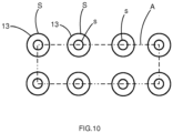
- the surfaces of the receiving ends have an area substantially greater than the area of a section s of the body of the nanowire, for example at least 20% greater, or even at least 50% greater.
- the section s considered of the body of the nanowire is positioned parallel to the receiving end or perpendicular to the axis A.
- the section s considered is positioned at least 2 ⁇ m away from the end reception.
- the considered section s of the nanowire is parallel to the receiving end in the middle of the nanowire or in the middle of the body of the nanowire.
- the area of the nanowires in contact with the membrane is significantly greater than the projected area of the base of the nanowires (perpendicular to the direction A along which the nanowires extend).
- the area of the nanowires in contact with the membrane can be greater than 10 times the projected area of the base of the nanowires.
- the head is distinguished from the body by a variation of at least one dimension measured transversely to the direction A along which the nanowire extends.
- the limit between the body and the head can for example be defined by an increase in a significant transverse dimension of the body, in particular an increase of more than 10%. More generally, the head has at least one transverse dimension greater than a transverse dimension of the body.
- the heads are frustoconical with a polygonal section or include a trunk of cone with polygonal section.
- the small base of the truncated cone is in contact with the body.
- the heads are stacks of a layer 121 of p-type GaN and a layer 122 of p++ type GaN.
- the heads can also be made differently, in particular in other exemplary embodiments, the layer 121 can be made up of InGaN and topped with a conformal or enlarged layer in turn of p-type GaN, itself topped with a conformal or enlarged layer in turn of p++ type GaN.
- Layer 121 is for example frustoconical with a polygonal section. One face of layer 122 forms the receiving end.
- the different receiving ends form a discontinuous surface. Indeed, between the different receiving ends, it is possible to connect the surfaces of the receiving ends to produce a continuous surface, in particular a surface without significant curvature discontinuity.
- the connected discontinuous surface may be planar or substantially planar. More generally, this connected discontinuous surface can also be a non-planar ruled surface or a left surface.
- the ratio of the sum of the areas of the surfaces of the receiving ends relative to the total area of the discontinuous surface connected between the receiving ends is for example greater than 80% or greater than 90% or greater than 95%.
- the membrane is in contact with the nanowires over more than 80% or more than 90% or more than 95% of its surface.
- the geometries of the heads therefore define a surface density of material against which the membrane can come into contact. This density is very important. The higher it is, the less risk there is of tearing or piercing the membrane when placing it on the nanowires and the more good electrical contact is ensured between the membrane and the nanowires.
- the membrane can be pierced, particularly at the edge of the structure, due to the fineness of the nanowires and/or the large distance which separates them. Such damage is of course not desirable.
- the density of the presence of matter (expressed as a percentage above) is sufficiently high.
- a nanowire device as described above is used.
- the combination of a high density of nanowires and a device with nanowires with particular geometry as described above are favorable for the transfer of a membrane without damage or tearing.
- the ratio of the sum of the areas of the surfaces of the receiving ends relative to the total area of the connected discontinuous surface between the receiving ends is for example strictly less than 100%.
- the transfer of the membrane can also be carried out in the case where the nanowires are further away from each other.
- the distance between the nanowires in other words the pitch of the nanowire network, can be greater than or equal to at least five times the transverse dimension of the body of the nanowires.
- the pitch of the nanowire network will be adjusted depending in particular on the mechanical resistance of the material forming the membrane.
- the heads of the nanowires may not be frustoconical with a polygonal section, but may have any other shape.
- the heads can be prismatic as shown in the Figure 3 .
- the diameter of the head 12' is greater than the diameter of the body 11'.
- the nanowires may not have a light-emitting diode structure. Indeed, a nanowire structure as described above may not be used to emit light.
- the nanowires can in particular be made from a material based on silicon or based on any other semiconductor material such as those belonging to the arsenide family or based on any other material (metal, polymer, ceramic). on which there is an interest in depositing a membrane making it possible to ensure the continuity of an electrical injection and/or the application of a potential.
- a membrane device 3, 34 is produced, comprising the membrane 3 covered with a layer 34.
- a nanowire device 10 is produced or shaped as described above or a nanowire device which differs from what has been described previously in that the nanowires have a structure in which a head cannot be distinguished. of a body, that is to say for example a structure with constant or substantially constant dimension or cross section over the entire length of the nanowires.
- the nanowires of device 10 form a discontinuous structure.
- the nanowires are non-coalesced, each at a distance from the others.
- the ends of the nanowires, called receiving ends of the membrane or receiving ends form a discontinuous surface.
- a fourth phase the structure is rinsed with a solvent, for example acetone, in particular so as to dissolve a layer 34 of the membrane device, in particular so as to dissolve a layer of resin from the membrane device.
- a solvent for example acetone
- the second material may be identical to the first material. This optional deposition step makes it possible, for example, to mechanically reinforce the membrane by thickening it.
- the first and second phases can be performed in any order. They can also be executed in parallel or simultaneously.
- a second substrate 31 is provided, for example a silicon wafer.
- a sacrificial layer 32 is deposited on the second substrate, for example a layer of metal, in particular a layer of nickel or copper.
- a layer 3 of the first material is deposited on the sacrificial layer, in particular for example a layer of approximately 30 nm thick or a layer of approximately 20 nm thick. This layer constitutes membrane 3.
- a layer 34 of resin is deposited on the layer of first material.
- the sacrificial layer 32 is chemically attacked, for example with a solution of FeCl 3 .
- a membrane formed of layers 3 and 34 as shown in the Figure 7 .
- the device 10 is shaped or produced, for example by molecular beam epitaxy or by organometallic vapor phase epitaxy or by etching.
- a judicious choice of the parameters of the process used makes it possible to obtain an enlarged head.
- a judicious choice of the growth conditions of the nanowires by molecular beam epitaxy makes it possible to obtain an enlarged head.
- an electrode transparent and conductive
- micro or nano pillars each comprising at its top a flat surface of dimension greater than the diameter of said pillars.
- the production is ensured by placing or transferring a membrane (transparent and conductive) on these summit surfaces.
- the geometry and density of the top surfaces make it possible to obtain optimized electrical contact while avoiding the possible piercing of the membrane by the pillars.
- the membrane makes it possible to ensure electrical continuity on the discontinuous structure of the nanowire device.
- an interesting application of the invention concerns the production of LED structures. It should be noted that in the case of organic LEDs which can be damaged by conventional techniques for deposition of metallic layers, the transfer solution is a gentle technique which allows the integrity of a membrane to be preserved during its installation. .
- any structure with wire elements can be concerned by the device and the method which is the subject of this document, independently of the density or the size of the wire elements. We can thus envisage making contact in particular on single photon emitters or on various photonic objects (microdiscs).
- conductive membranes are not a priori limited to the field of LEDs. This type of membrane can also be transferred to any type of nanowires or nanopillars obtained by “bottom-up” or “top-down” technology.
- ITO membrane The transfer of an indium tin oxide or ITO membrane has been described previously. However, in addition to ITO, any membrane made of another material can a priori be used, provided that it can be easily detached from the initial support, for example via chemical attack on a sacrificial layer.
Landscapes
- Led Devices (AREA)
- Light Receiving Elements (AREA)
- Crystals, And After-Treatments Of Crystals (AREA)
- Inorganic Fibers (AREA)
Claims (13)
- Verfahren zur Herstellung einer Struktur (100), die eine Membran (3) aus einem ersten Material, insbesondere Indiumzinnoxid, in Kontakt mit Empfangsenden (13) einer Vielzahl von Nanodrähten (1) enthält, wobei das Verfahren die folgenden Schritte enthält:- Gestaltung einer Vorrichtung (10) mit Nanodrähten, die die Empfangsenden (13) enthält, wobei die Empfangsenden so gestaltet sind, dass sie ebene Flächen bilden,- Herstellung einer Membranvorrichtung (3; 34), die die Membran (3) und eine Schicht (34) enthält,- Einsetzen, durch Verschiebung, der vorher hergestellten Membranvorrichtung (3; 34) direkt auf die Nanodrähte im Bereich der ebenen Flächen der Empfangsenden, so dass die Membran mit den Empfangsenden in Kontakt ist, wobei das Verhältnis der Summe der Flächeninhalte der Flächen der Empfangsenden bezogen auf den kontinuierlichen Flächeninhalt der Fläche der Membran auf den Empfangsenden strikt niedriger als 100% ist, und- nach dem Schritt des Einsetzens des Membranvorrichtung auf die Nanodrähte im Bereich der Empfangsenden, Spülen der Struktur mit einem Lösungsmittel, um die Schicht (34) der Membranvorrichtung aufzulösen, um die Membran (3) auf den Empfangsenden zu behalten.
- Verfahren nach Anspruch 1, dadurch gekennzeichnet, dass es einen Schritt des Abscheidens einer Schicht (4) eines zweiten elektrisch leitenden Materials auf die Membran (3) enthält, insbesondere einen Schritt des Abscheidens einer Schicht eines zweiten Materials gleich dem ersten Material.
- Verfahren nach einem der vorhergehenden Ansprüche, dadurch gekennzeichnet, dass die Membran transparent und elektrisch leitend ist und/oder dass die Membran dazu bestimmt ist, eine Elektrode zu bilden, und/oder dass Nanodrähte Strukturen von Elektrolumineszenzdioden sind.
- Verfahren nach einem der vorhergehenden Ansprüche, dadurch gekennzeichnet, dass der Schritt der Herstellung der Membranvorrichtung (3, 34) die folgenden Schritte enthält:- Bereitstellen eines zweiten Substrats (31), insbesondere eines Siliciumplättchens;- Abscheiden einer Opferschicht (32), vor allem von Metall, insbesondere von Nickel oder Kupfer, auf das zweite Substrat,- Abscheiden einer Schicht (3) eines ersten Materials, die dazu bestimmt ist, die Membran zu bilden, auf die Opferschicht, insbesondere einer Schicht von etwa 30 nm Dicke,- Abscheiden einer Harzschicht (34) auf die Schicht eines ersten Materials, wobei die Membran (3) und die Harzschicht (34) die Membranvorrichtung bilden,- Chemisches Ätzen der Opferschicht, zum Beispiel mit einer Lösung von FeCl3, um die Membranvorrichtung vom zweiten Substrat zu lösen.
- Verfahren nach einem der vorhergehenden Ansprüche, dadurch gekennzeichnet, dass der Schritt der Gestaltung der Vorrichtung mit Nanodrähten durch Molekularstrahlepitaxie oder durch metallorganische Gasphasenepitaxie oder durch Ätzen durchgeführt wird.
- Verfahren nach einem der vorhergehenden Ansprüche, dadurch gekennzeichnet, dass der Schritt der Gestaltung die Gestaltung der Vorrichtung derart enthält, dass sie ein erstes Substrat (2) enthält, wobei die Nanodrähte auf dem ersten Substrat angeordnet sind, wobei vor allem die Nanodrähte lotrecht oder im Wesentlichen lotrecht auf einer Fläche (21) des ersten Substrats angeordnet sind, und/oder dass die Nanodrähte prismatisch oder im Wesentlichen sind und/oder dass die Nanodrähte Strukturen von Elektrolumineszenzdioden aufweisen.
- Verfahren nach einem der vorhergehenden Ansprüche, dadurch gekennzeichnet, dass der Schritt der Gestaltung die Gestaltung der Empfangsenden derart enthält, dass sie eine ebene oder im Wesentlichen ebene diskontinuierliche Fläche bilden.
- Verfahren nach dem vorhergehenden Anspruch, dadurch gekennzeichnet, dass der Schritt der Gestaltung die Gestaltung der Vorrichtung derart enthält, dass das Verhältnis der Summe der Flächeninhalte der Flächen der Empfangsenden bezogen auf den kontinuierlichen Flächeninhalt der Fläche einer Membran, die dazu bestimmt ist, mit den Empfangsenden in Kontakt zu kommen, größer ist als 80% oder größer als 90% oder größer als 95%.
- Verfahren nach einem der vorhergehenden Ansprüche, dadurch gekennzeichnet, dass der Schritt der Gestaltung die Gestaltung von Nanodrähten derart enthält, dass die Nanodrähte eine Geometrie aufweisen, die sich in Richtung der Empfangsenden vergrößert oder ausweitet und/oder dass der Schritt der Gestaltung die Gestaltung von Nanodrähten derart enthält, dass die Nanodrähte Mikrosäulen oder Nanosäulen bilden, die die Empfangsenden umfassen, deren Flächen Abmessungen größer als diejenigen der Durchmesser der Nanodrähte in Abstand zum Empfangsende aufweisen.
- Verfahren nach einem der vorhergehenden Ansprüche, dadurch gekennzeichnet, dass der Schritt der Gestaltung die Gestaltung von Nanodrähten derart enthält, dass sie je einen Körper (11; 11') und einen Kopf (12; 12') enthalten, wobei der Kopf ein Empfangsende (13) aufweist, wobei die Fläche des Empfangsendes einen Flächeninhalt aufweist, der 20% größer, sogar 50% größer ist als der Flächeninhalt eines Querschnitts (s) des Körpers eines Nanodrahts, vor allem als der Flächeninhalt eines Querschnitts (s) des Nanodrahts gemessen parallel zum Empfangsende in mindestens 2 µm Abstand zum Empfangsende oder als der Flächeninhalt eines Querschnitts (s) des Nanodrahts gemessen parallel zum Empfangsende in der Mitte des Nanodrahts.
- Verfahren nach dem vorhergehenden Anspruch, dadurch gekennzeichnet, dass der Schritt der Gestaltung die Gestaltung der Körper der Nanodrähte in Stapeln einer Schicht (111) von GaN vom n-Typ, einer Schicht (112) von InGaN und einer Sperrschicht (113) enthält.
- Verfahren nach einem der Ansprüche 10 und 11, dadurch gekennzeichnet, dass der Schritt der Gestaltung die Gestaltung der Köpfe der Nanodrähte in Stapeln einer Schicht (121) von GaN vom p-Typ und einer Schicht (122) von GaN vom p++-Typ enthält.
- Verfahren nach einem der Ansprüche 1 bis 10, dadurch gekennzeichnet, dass der Schritt der Gestaltung die Gestaltung der Nanodrähte aus einem Material auf der Basis von Silicium enthält.
Applications Claiming Priority (2)
| Application Number | Priority Date | Filing Date | Title |
|---|---|---|---|
| FR1752286A FR3064109B1 (fr) | 2017-03-20 | 2017-03-20 | Structure a nanofils et procede de realisation d'une telle structure |
| PCT/EP2018/056881 WO2018172281A1 (fr) | 2017-03-20 | 2018-03-19 | Structure a nanofils et procede de realisation d'une telle structure |
Publications (3)
| Publication Number | Publication Date |
|---|---|
| EP3602640A1 EP3602640A1 (de) | 2020-02-05 |
| EP3602640B1 true EP3602640B1 (de) | 2024-07-24 |
| EP3602640C0 EP3602640C0 (de) | 2024-07-24 |
Family
ID=58707864
Family Applications (1)
| Application Number | Title | Priority Date | Filing Date |
|---|---|---|---|
| EP18711346.9A Active EP3602640B1 (de) | 2017-03-20 | 2018-03-19 | Nanodrahtstruktur und verfahren zu ihrer herstellung |
Country Status (7)
| Country | Link |
|---|---|
| US (1) | US11189752B2 (de) |
| EP (1) | EP3602640B1 (de) |
| JP (1) | JP7370863B2 (de) |
| KR (1) | KR102582831B1 (de) |
| CN (1) | CN110582858B (de) |
| FR (1) | FR3064109B1 (de) |
| WO (1) | WO2018172281A1 (de) |
Families Citing this family (3)
| Publication number | Priority date | Publication date | Assignee | Title |
|---|---|---|---|---|
| US20200091388A1 (en) | 2018-09-19 | 2020-03-19 | Vuereal Inc. | Highly efficient microdevices |
| KR102701758B1 (ko) | 2018-11-27 | 2024-09-04 | 삼성디스플레이 주식회사 | 발광 소자, 이의 제조 방법 및 발광 소자를 구비한 표시 장치 |
| CN113451108B (zh) * | 2020-03-24 | 2024-06-25 | 中国科学院苏州纳米技术与纳米仿生研究所 | 一种超柔性透明半导体薄膜及其制备方法 |
Citations (3)
| Publication number | Priority date | Publication date | Assignee | Title |
|---|---|---|---|---|
| WO2013165135A1 (ko) * | 2012-05-01 | 2013-11-07 | 주식회사 칩테크놀러지 | 반도체 발광 칩 및 그의 제조 방법 |
| FR3007574A1 (fr) * | 2013-06-21 | 2014-12-26 | Commissariat Energie Atomique | Procede de fabrication d'une structure semiconductrice et composant semiconducteur comportant une telle structure semiconductrice |
| US20150155443A1 (en) * | 2012-06-14 | 2015-06-04 | Konica Minolta, Inc. | Electroluminescent Element and Lighting Apparatus Comprising the Same |
Family Cites Families (28)
| Publication number | Priority date | Publication date | Assignee | Title |
|---|---|---|---|---|
| JP2002208483A (ja) * | 2001-01-11 | 2002-07-26 | Sharp Corp | 有機エレクトロルミネッセンス素子およびその製造方法 |
| TWI442456B (zh) * | 2004-08-31 | 2014-06-21 | Sophia School Corp | 發光元件 |
| KR100765722B1 (ko) * | 2005-05-27 | 2007-10-11 | 엘지전자 주식회사 | 나노 로드를 갖는 발광 소자 및 그의 제조 방법 |
| KR20070021671A (ko) * | 2005-08-19 | 2007-02-23 | 서울옵토디바이스주식회사 | 나노막대들의 어레이를 채택한 발광 다이오드 및 그것을제조하는 방법 |
| EP2091862B1 (de) * | 2006-12-22 | 2019-12-11 | QuNano AB | Erhöhte led und herstellungsverfahren dafür |
| JP5097460B2 (ja) * | 2007-06-26 | 2012-12-12 | パナソニック株式会社 | 化合物半導体素子およびそれを用いる照明装置ならびに化合物半導体素子の製造方法 |
| KR20100056478A (ko) * | 2007-08-21 | 2010-05-27 | 더 리전트 오브 더 유니버시티 오브 캘리포니아 | 고성능 열전 속성을 갖는 나노구조체 |
| JP5097532B2 (ja) * | 2007-12-21 | 2012-12-12 | パナソニック株式会社 | 化合物半導体発光素子の製造方法 |
| KR101469979B1 (ko) | 2008-03-24 | 2014-12-05 | 엘지이노텍 주식회사 | 그룹 3족 질화물계 반도체 발광다이오드 소자 및 이의 제조방법 |
| WO2009125983A2 (ko) * | 2008-04-08 | 2009-10-15 | Song June O | 발광 소자 및 그 제조방법 |
| FR2984599B1 (fr) * | 2011-12-20 | 2014-01-17 | Commissariat Energie Atomique | Procede de fabrication d'un micro- ou nano- fil semiconducteur, structure semiconductrice comportant un tel micro- ou nano- fil et procede de fabrication d'une structure semiconductrice |
| FR2988904B1 (fr) * | 2012-04-02 | 2015-01-16 | Commissariat Energie Atomique | Structure semiconductrice optoelectronique a nanofils et procede de fabrication d'une telle structure |
| TWI541992B (zh) * | 2012-05-14 | 2016-07-11 | 國立清華大學 | 發光二極體顯示器與其製造方法 |
| CN102709410B (zh) * | 2012-06-04 | 2014-08-27 | 中国科学院半导体研究所 | 纳米柱发光二极管的制作方法 |
| CN102881762A (zh) * | 2012-10-17 | 2013-01-16 | 长春理工大学 | MgZnO纳米线阵列紫外光电探测器 |
| US9012883B2 (en) * | 2012-12-21 | 2015-04-21 | Sol Voltaics Ab | Recessed contact to semiconductor nanowires |
| FR3004006B1 (fr) * | 2013-03-28 | 2016-10-07 | Aledia | Dispositif electroluminescent a nanofils actifs et nanofils de contact et procede de fabrication |
| JP6147542B2 (ja) * | 2013-04-01 | 2017-06-14 | 株式会社東芝 | 透明導電フィルムおよび電気素子 |
| CN103681962B (zh) * | 2013-11-21 | 2016-02-17 | 中国科学院上海技术物理研究所 | 基于竖直排列半导体纳米线的光电探测器制备方法 |
| CN103943754A (zh) * | 2014-03-06 | 2014-07-23 | 京东方科技集团股份有限公司 | 一种电致发光器件及其制备方法和显示装置 |
| JP2015212213A (ja) * | 2014-05-07 | 2015-11-26 | 国立大学法人 名古屋工業大学 | グラフェンシートとの一体化ZnOナノロッド、およびグラフェンシート上へのZnOナノロッドの製造方法 |
| JP6482388B2 (ja) * | 2015-06-02 | 2019-03-13 | シャープ株式会社 | 窒化物半導体発光素子 |
| US10290767B2 (en) * | 2015-06-09 | 2019-05-14 | The Royal Institution For The Advancement Of Learning/Mcgill University | High efficiency visible and ultraviolet nanowire emitters |
| DK3323152T3 (da) * | 2015-07-13 | 2021-12-20 | Crayonano As | Nanowire-/nanopyramideformede lysdioder og fotodetektorer |
| WO2017068450A1 (en) * | 2015-10-20 | 2017-04-27 | King Abdullah University Of Science And Technology | Nanowires-based light emitters on thermally and electrically conductive substrates and of making same |
| FR3044470B1 (fr) * | 2015-11-30 | 2018-03-23 | Commissariat A L'energie Atomique Et Aux Energies Alternatives | Dispositif optoelectronique comportant des structures semiconductrices tridimensionnelles en configuration axiale |
| CN105741979B (zh) * | 2016-03-02 | 2018-03-30 | 武汉华星光电技术有限公司 | 柔性石墨烯导电薄膜的制备方法 |
| US10651343B2 (en) * | 2017-02-28 | 2020-05-12 | King Abdullah University Of Science And Technology | Integration of III-nitride nanowire on transparent conductive substrates for optoelectronic and electronic devices |
-
2017
- 2017-03-20 FR FR1752286A patent/FR3064109B1/fr active Active
-
2018
- 2018-03-19 WO PCT/EP2018/056881 patent/WO2018172281A1/fr not_active Ceased
- 2018-03-19 US US16/495,579 patent/US11189752B2/en active Active
- 2018-03-19 EP EP18711346.9A patent/EP3602640B1/de active Active
- 2018-03-19 CN CN201880029732.XA patent/CN110582858B/zh active Active
- 2018-03-19 KR KR1020197030967A patent/KR102582831B1/ko active Active
- 2018-03-19 JP JP2019552287A patent/JP7370863B2/ja active Active
Patent Citations (4)
| Publication number | Priority date | Publication date | Assignee | Title |
|---|---|---|---|---|
| WO2013165135A1 (ko) * | 2012-05-01 | 2013-11-07 | 주식회사 칩테크놀러지 | 반도체 발광 칩 및 그의 제조 방법 |
| KR101338148B1 (ko) * | 2012-05-01 | 2014-01-06 | 주식회사 칩테크놀러지 | 반도체 발광 칩 및 그의 제조 방법 |
| US20150155443A1 (en) * | 2012-06-14 | 2015-06-04 | Konica Minolta, Inc. | Electroluminescent Element and Lighting Apparatus Comprising the Same |
| FR3007574A1 (fr) * | 2013-06-21 | 2014-12-26 | Commissariat Energie Atomique | Procede de fabrication d'une structure semiconductrice et composant semiconducteur comportant une telle structure semiconductrice |
Also Published As
| Publication number | Publication date |
|---|---|
| US20200028027A1 (en) | 2020-01-23 |
| JP2020515078A (ja) | 2020-05-21 |
| CN110582858B (zh) | 2023-01-13 |
| KR20190131076A (ko) | 2019-11-25 |
| FR3064109B1 (fr) | 2025-03-14 |
| EP3602640C0 (de) | 2024-07-24 |
| WO2018172281A1 (fr) | 2018-09-27 |
| US11189752B2 (en) | 2021-11-30 |
| KR102582831B1 (ko) | 2023-09-25 |
| JP7370863B2 (ja) | 2023-10-30 |
| FR3064109A1 (fr) | 2018-09-21 |
| CN110582858A (zh) | 2019-12-17 |
| EP3602640A1 (de) | 2020-02-05 |
Similar Documents
| Publication | Publication Date | Title |
|---|---|---|
| EP2203939B1 (de) | Optoelektronische anordnung mit nanodrähten und entsprechende verfahren | |
| EP2491591B1 (de) | Herstellungsverfahren eines sehr hochauflösenden bildschirms mit einer anisotropischen emittierenden leiterschicht auf basis von lichtemittierenden dioden nanodrähten und entsprechendem bildschirm | |
| EP2211387B1 (de) | Verfahren zur Herstellung eines homogenen pn-Übergangs in einer Nanostruktur | |
| EP3144272B1 (de) | Method for orienting elongate objects arranged on the surface of a substrate | |
| WO2012163899A1 (fr) | Structure semiconductrice destinée a émettre de la lumière et procede de fabrication d'une telle structure | |
| EP3602640B1 (de) | Nanodrahtstruktur und verfahren zu ihrer herstellung | |
| FR2923651A1 (fr) | Procede de realisation d'une jonction pn dans un nanofil, et d'un nanofil avec au moins une jonction pn. | |
| FR2967813A1 (fr) | Procédé de réalisation d'une structure a couche métallique enterrée | |
| EP3161883B1 (de) | Tandemzellen mit mehreren fäden | |
| FR3004006A1 (fr) | Dispositif electroluminescent a nanofils actifs et nanofils de contact et procede de fabrication | |
| EP2807681A1 (de) | Verfahren zur herstellung einer mikroelektronischen vorrichtung mit einer vielzahl von drahtleuchtdioden | |
| EP3891813B1 (de) | Mehrfarbige elektrolumineszierende anzeigevorrichtung und verfahren zur herstellung einer solchen vorrichtung | |
| EP3011603B1 (de) | Verfahren zur herstellung einer halbleiterstruktur und halbleiterkomponente mit solch einer halbleiterstruktur | |
| WO2018122517A1 (fr) | Procede de realisation d'un dispositif optoelectronique comportant une etape de gravure de la face arriere du substrat de croissance | |
| EP3836235B1 (de) | Verfahren zum aufbringen einer strukturierten materialschicht | |
| EP2827390B1 (de) | Emissionsstruktur mit seitlicher Einspritzung von Trägerstoffen | |
| EP3263519B1 (de) | Homogenisierungsverfahren der höhe einer vielzahl von fäden | |
| WO2020094944A1 (fr) | Procede de fabrication collective d'une pluralite de structures semi-conductrices | |
| FR3143850A1 (fr) | Procédé de réalisation d’un dispositif électronique |
Legal Events
| Date | Code | Title | Description |
|---|---|---|---|
| STAA | Information on the status of an ep patent application or granted ep patent |
Free format text: STATUS: UNKNOWN |
|
| STAA | Information on the status of an ep patent application or granted ep patent |
Free format text: STATUS: THE INTERNATIONAL PUBLICATION HAS BEEN MADE |
|
| PUAI | Public reference made under article 153(3) epc to a published international application that has entered the european phase |
Free format text: ORIGINAL CODE: 0009012 |
|
| STAA | Information on the status of an ep patent application or granted ep patent |
Free format text: STATUS: REQUEST FOR EXAMINATION WAS MADE |
|
| 17P | Request for examination filed |
Effective date: 20190927 |
|
| AK | Designated contracting states |
Kind code of ref document: A1 Designated state(s): AL AT BE BG CH CY CZ DE DK EE ES FI FR GB GR HR HU IE IS IT LI LT LU LV MC MK MT NL NO PL PT RO RS SE SI SK SM TR |
|
| AX | Request for extension of the european patent |
Extension state: BA ME |
|
| DAV | Request for validation of the european patent (deleted) | ||
| DAX | Request for extension of the european patent (deleted) | ||
| STAA | Information on the status of an ep patent application or granted ep patent |
Free format text: STATUS: EXAMINATION IS IN PROGRESS |
|
| 17Q | First examination report despatched |
Effective date: 20200914 |
|
| GRAP | Despatch of communication of intention to grant a patent |
Free format text: ORIGINAL CODE: EPIDOSNIGR1 |
|
| STAA | Information on the status of an ep patent application or granted ep patent |
Free format text: STATUS: GRANT OF PATENT IS INTENDED |
|
| INTG | Intention to grant announced |
Effective date: 20240219 |
|
| GRAS | Grant fee paid |
Free format text: ORIGINAL CODE: EPIDOSNIGR3 |
|
| GRAA | (expected) grant |
Free format text: ORIGINAL CODE: 0009210 |
|
| STAA | Information on the status of an ep patent application or granted ep patent |
Free format text: STATUS: THE PATENT HAS BEEN GRANTED |
|
| AK | Designated contracting states |
Kind code of ref document: B1 Designated state(s): AL AT BE BG CH CY CZ DE DK EE ES FI FR GB GR HR HU IE IS IT LI LT LU LV MC MK MT NL NO PL PT RO RS SE SI SK SM TR |
|
| REG | Reference to a national code |
Ref country code: GB Ref legal event code: FG4D Free format text: NOT ENGLISH |
|
| REG | Reference to a national code |
Ref country code: CH Ref legal event code: EP |
|
| REG | Reference to a national code |
Ref country code: IE Ref legal event code: FG4D Free format text: LANGUAGE OF EP DOCUMENT: FRENCH Ref country code: DE Ref legal event code: R096 Ref document number: 602018072129 Country of ref document: DE |
|
| U01 | Request for unitary effect filed |
Effective date: 20240821 |
|
| U07 | Unitary effect registered |
Designated state(s): AT BE BG DE DK EE FI FR IT LT LU LV MT NL PT RO SE SI Effective date: 20240902 |
|
| RAP4 | Party data changed (patent owner data changed or rights of a patent transferred) |
Owner name: COMMISSARIAT A L'ENERGIE ATOMIQUE ET AUX ENERGIESALTERNATIVES |
|
| U1H | Name or address of the proprietor changed after the registration of the unitary effect |
Owner name: COMMISSARIAT A L'ENERGIE ATOMIQUE ET AUX ENERGIESALTERNATIVES; FR |
|
| PG25 | Lapsed in a contracting state [announced via postgrant information from national office to epo] |
Ref country code: NO Free format text: LAPSE BECAUSE OF FAILURE TO SUBMIT A TRANSLATION OF THE DESCRIPTION OR TO PAY THE FEE WITHIN THE PRESCRIBED TIME-LIMIT Effective date: 20241024 |
|
| PG25 | Lapsed in a contracting state [announced via postgrant information from national office to epo] |
Ref country code: GR Free format text: LAPSE BECAUSE OF FAILURE TO SUBMIT A TRANSLATION OF THE DESCRIPTION OR TO PAY THE FEE WITHIN THE PRESCRIBED TIME-LIMIT Effective date: 20241025 Ref country code: PL Free format text: LAPSE BECAUSE OF FAILURE TO SUBMIT A TRANSLATION OF THE DESCRIPTION OR TO PAY THE FEE WITHIN THE PRESCRIBED TIME-LIMIT Effective date: 20240724 |
|
| PG25 | Lapsed in a contracting state [announced via postgrant information from national office to epo] |
Ref country code: IS Free format text: LAPSE BECAUSE OF FAILURE TO SUBMIT A TRANSLATION OF THE DESCRIPTION OR TO PAY THE FEE WITHIN THE PRESCRIBED TIME-LIMIT Effective date: 20241124 |
|
| PG25 | Lapsed in a contracting state [announced via postgrant information from national office to epo] |
Ref country code: HR Free format text: LAPSE BECAUSE OF FAILURE TO SUBMIT A TRANSLATION OF THE DESCRIPTION OR TO PAY THE FEE WITHIN THE PRESCRIBED TIME-LIMIT Effective date: 20240724 |
|
| PG25 | Lapsed in a contracting state [announced via postgrant information from national office to epo] |
Ref country code: RS Free format text: LAPSE BECAUSE OF FAILURE TO SUBMIT A TRANSLATION OF THE DESCRIPTION OR TO PAY THE FEE WITHIN THE PRESCRIBED TIME-LIMIT Effective date: 20241024 Ref country code: ES Free format text: LAPSE BECAUSE OF FAILURE TO SUBMIT A TRANSLATION OF THE DESCRIPTION OR TO PAY THE FEE WITHIN THE PRESCRIBED TIME-LIMIT Effective date: 20240724 |
|
| PG25 | Lapsed in a contracting state [announced via postgrant information from national office to epo] |
Ref country code: RS Free format text: LAPSE BECAUSE OF FAILURE TO SUBMIT A TRANSLATION OF THE DESCRIPTION OR TO PAY THE FEE WITHIN THE PRESCRIBED TIME-LIMIT Effective date: 20241024 Ref country code: PL Free format text: LAPSE BECAUSE OF FAILURE TO SUBMIT A TRANSLATION OF THE DESCRIPTION OR TO PAY THE FEE WITHIN THE PRESCRIBED TIME-LIMIT Effective date: 20240724 Ref country code: NO Free format text: LAPSE BECAUSE OF FAILURE TO SUBMIT A TRANSLATION OF THE DESCRIPTION OR TO PAY THE FEE WITHIN THE PRESCRIBED TIME-LIMIT Effective date: 20241024 Ref country code: IS Free format text: LAPSE BECAUSE OF FAILURE TO SUBMIT A TRANSLATION OF THE DESCRIPTION OR TO PAY THE FEE WITHIN THE PRESCRIBED TIME-LIMIT Effective date: 20241124 Ref country code: HR Free format text: LAPSE BECAUSE OF FAILURE TO SUBMIT A TRANSLATION OF THE DESCRIPTION OR TO PAY THE FEE WITHIN THE PRESCRIBED TIME-LIMIT Effective date: 20240724 Ref country code: GR Free format text: LAPSE BECAUSE OF FAILURE TO SUBMIT A TRANSLATION OF THE DESCRIPTION OR TO PAY THE FEE WITHIN THE PRESCRIBED TIME-LIMIT Effective date: 20241025 Ref country code: ES Free format text: LAPSE BECAUSE OF FAILURE TO SUBMIT A TRANSLATION OF THE DESCRIPTION OR TO PAY THE FEE WITHIN THE PRESCRIBED TIME-LIMIT Effective date: 20240724 |
|
| U20 | Renewal fee for the european patent with unitary effect paid |
Year of fee payment: 8 Effective date: 20250225 |
|
| PG25 | Lapsed in a contracting state [announced via postgrant information from national office to epo] |
Ref country code: SM Free format text: LAPSE BECAUSE OF FAILURE TO SUBMIT A TRANSLATION OF THE DESCRIPTION OR TO PAY THE FEE WITHIN THE PRESCRIBED TIME-LIMIT Effective date: 20240724 |
|
| PG25 | Lapsed in a contracting state [announced via postgrant information from national office to epo] |
Ref country code: CZ Free format text: LAPSE BECAUSE OF FAILURE TO SUBMIT A TRANSLATION OF THE DESCRIPTION OR TO PAY THE FEE WITHIN THE PRESCRIBED TIME-LIMIT Effective date: 20240724 |
|
| PG25 | Lapsed in a contracting state [announced via postgrant information from national office to epo] |
Ref country code: SK Free format text: LAPSE BECAUSE OF FAILURE TO SUBMIT A TRANSLATION OF THE DESCRIPTION OR TO PAY THE FEE WITHIN THE PRESCRIBED TIME-LIMIT Effective date: 20240724 |
|
| PGFP | Annual fee paid to national office [announced via postgrant information from national office to epo] |
Ref country code: GB Payment date: 20250324 Year of fee payment: 8 |
|
| PLBE | No opposition filed within time limit |
Free format text: ORIGINAL CODE: 0009261 |
|
| STAA | Information on the status of an ep patent application or granted ep patent |
Free format text: STATUS: NO OPPOSITION FILED WITHIN TIME LIMIT |
|
| 26N | No opposition filed |
Effective date: 20250425 |
|
| PG25 | Lapsed in a contracting state [announced via postgrant information from national office to epo] |
Ref country code: MC Free format text: LAPSE BECAUSE OF FAILURE TO SUBMIT A TRANSLATION OF THE DESCRIPTION OR TO PAY THE FEE WITHIN THE PRESCRIBED TIME-LIMIT Effective date: 20240724 |
|
| REG | Reference to a national code |
Ref country code: CH Ref legal event code: H13 Free format text: ST27 STATUS EVENT CODE: U-0-0-H10-H13 (AS PROVIDED BY THE NATIONAL OFFICE) Effective date: 20251023 |