EP3588682B1 - Kontakt für direktsteckverbindung und direktsteckverbindung - Google Patents
Kontakt für direktsteckverbindung und direktsteckverbindung Download PDFInfo
- Publication number
- EP3588682B1 EP3588682B1 EP19179478.3A EP19179478A EP3588682B1 EP 3588682 B1 EP3588682 B1 EP 3588682B1 EP 19179478 A EP19179478 A EP 19179478A EP 3588682 B1 EP3588682 B1 EP 3588682B1
- Authority
- EP
- European Patent Office
- Prior art keywords
- contact
- strip
- bulge
- section
- circuit board
- Prior art date
- Legal status (The legal status is an assumption and is not a legal conclusion. Google has not performed a legal analysis and makes no representation as to the accuracy of the status listed.)
- Active
Links
Images



Classifications
-
- H—ELECTRICITY
- H01—ELECTRIC ELEMENTS
- H01R—ELECTRICALLY-CONDUCTIVE CONNECTIONS; STRUCTURAL ASSOCIATIONS OF A PLURALITY OF MUTUALLY-INSULATED ELECTRICAL CONNECTING ELEMENTS; COUPLING DEVICES; CURRENT COLLECTORS
- H01R12/00—Structural associations of a plurality of mutually-insulated electrical connecting elements, specially adapted for printed circuits, e.g. printed circuit boards [PCB], flat or ribbon cables, or like generally planar structures, e.g. terminal strips, terminal blocks; Coupling devices specially adapted for printed circuits, flat or ribbon cables, or like generally planar structures; Terminals specially adapted for contact with, or insertion into, printed circuits, flat or ribbon cables, or like generally planar structures
- H01R12/50—Fixed connections
- H01R12/51—Fixed connections for rigid printed circuits or like structures
- H01R12/55—Fixed connections for rigid printed circuits or like structures characterised by the terminals
- H01R12/58—Fixed connections for rigid printed circuits or like structures characterised by the terminals terminals for insertion into holes
- H01R12/585—Terminals having a press fit or a compliant portion and a shank passing through a hole in the printed circuit board
-
- H—ELECTRICITY
- H01—ELECTRIC ELEMENTS
- H01R—ELECTRICALLY-CONDUCTIVE CONNECTIONS; STRUCTURAL ASSOCIATIONS OF A PLURALITY OF MUTUALLY-INSULATED ELECTRICAL CONNECTING ELEMENTS; COUPLING DEVICES; CURRENT COLLECTORS
- H01R12/00—Structural associations of a plurality of mutually-insulated electrical connecting elements, specially adapted for printed circuits, e.g. printed circuit boards [PCB], flat or ribbon cables, or like generally planar structures, e.g. terminal strips, terminal blocks; Coupling devices specially adapted for printed circuits, flat or ribbon cables, or like generally planar structures; Terminals specially adapted for contact with, or insertion into, printed circuits, flat or ribbon cables, or like generally planar structures
- H01R12/70—Coupling devices
-
- H—ELECTRICITY
- H01—ELECTRIC ELEMENTS
- H01R—ELECTRICALLY-CONDUCTIVE CONNECTIONS; STRUCTURAL ASSOCIATIONS OF A PLURALITY OF MUTUALLY-INSULATED ELECTRICAL CONNECTING ELEMENTS; COUPLING DEVICES; CURRENT COLLECTORS
- H01R13/00—Details of coupling devices of the kinds covered by groups H01R12/70 or H01R24/00 - H01R33/00
- H01R13/40—Securing contact members in or to a base or case; Insulating of contact members
- H01R13/405—Securing in non-demountable manner, e.g. moulding, riveting
- H01R13/415—Securing in non-demountable manner, e.g. moulding, riveting by permanent deformation of contact member
-
- H—ELECTRICITY
- H01—ELECTRIC ELEMENTS
- H01R—ELECTRICALLY-CONDUCTIVE CONNECTIONS; STRUCTURAL ASSOCIATIONS OF A PLURALITY OF MUTUALLY-INSULATED ELECTRICAL CONNECTING ELEMENTS; COUPLING DEVICES; CURRENT COLLECTORS
- H01R12/00—Structural associations of a plurality of mutually-insulated electrical connecting elements, specially adapted for printed circuits, e.g. printed circuit boards [PCB], flat or ribbon cables, or like generally planar structures, e.g. terminal strips, terminal blocks; Coupling devices specially adapted for printed circuits, flat or ribbon cables, or like generally planar structures; Terminals specially adapted for contact with, or insertion into, printed circuits, flat or ribbon cables, or like generally planar structures
- H01R12/50—Fixed connections
- H01R12/51—Fixed connections for rigid printed circuits or like structures
- H01R12/53—Fixed connections for rigid printed circuits or like structures connecting to cables except for flat or ribbon cables
-
- H—ELECTRICITY
- H01—ELECTRIC ELEMENTS
- H01R—ELECTRICALLY-CONDUCTIVE CONNECTIONS; STRUCTURAL ASSOCIATIONS OF A PLURALITY OF MUTUALLY-INSULATED ELECTRICAL CONNECTING ELEMENTS; COUPLING DEVICES; CURRENT COLLECTORS
- H01R13/00—Details of coupling devices of the kinds covered by groups H01R12/70 or H01R24/00 - H01R33/00
- H01R13/02—Contact members
Definitions
- the invention relates to a contact for a direct plug-in connection with a connection section for connecting a cable strand and a contact section for making electrical contact with a through-hole in a circuit board and an insertion section forming a free end of the contact, the contact section and the insertion section on a strip of sheet metal material are formed with two side edges, a front and a back.
- the invention also relates to a direct plug-in connection with at least one plug and a printed circuit board, the printed circuit board having at least one through opening which is designed to be electrically conductive on the inside.
- a contact which has a strip of sheet-like sheet metal material, the strip being bent over its entire width and thereby forming a bulge.
- a contact for a direct plug connection is known, which is formed in one piece, wherein a strip of sheet metal material is provided with a central recess and then twisted. The twisted area is then used to make contact with a through hole in a printed circuit board.
- a contact for a direct plug connection according to the preamble of claim 1 is known, the contact having a hollow cylindrical design in the area which is provided for contacting a through hole of a circuit board.
- the hollow-cylindrical design is created by placing two half-cylinders on top of one another, each of which is formed by bulging out a sheet-metal strip.
- the contact according to the invention relates to a direct plug-in connection with a connection section for connecting a cable strand and a contact section for making electrical contact with a through-hole in a printed circuit board and an insertion section forming a free end of the contact, the contact section and the insertion section on a strip of sheet metal material with two Side edges, a front side and a rear side are formed, wherein the strip in the contact section on the front side or the rear side has a convex bulge to rest against the inside of the through opening.
- the strip Since the strip has a convex bulge to bear against the inside of the through opening, the area of a contact area with the inside of the through opening of a circuit board can be enlarged. Above all, it is possible to process galvanized raw material, since further post-processing, especially post-processing by electroplating, is not necessary.
- the contact can be used in a particularly advantageous manner for a so-called SKEDD direct plug connection.
- the convex bulge can be designed in any way, for example as a spherical segment, oval design, free-form surface or the like.
- the convex bulge is designed in such a way that there is point, line or area contact with the inside of the through opening of the circuit board.
- Flat-shaped contacts are obtained when the radii of the through opening in the circuit board and the convex bulge are approximately the same, preferably are the same.
- the convex bulge is spaced from the side edges of the strip.
- pre-treated or pre-coated sheet metal materials can be used in a particularly advantageous manner.
- the convex bulge is arranged on the front side of the strip and a concave depression is arranged on the rear side of the strip, opposite the convex bulge.
- the concave depression is formed as an impression and the convex bulge is formed as an impression.
- the convex bulge can be produced in a very simple and reliable manner by means of a simple embossing process.
- connection section is arranged between the connection section and the contact section, the connection section, the contact section and the insertion section being formed from a strip of sheet metal material and the strip having a first bending point between the connection section and the contact section at which the strip is twisted is.
- the convex bulge in the Contact portion are arranged so that when the contact is inserted into a through-opening of a circuit board, it reliably comes into contact with the inner wall of the through-opening.
- the strip has a second bending point between the contact section and the insertion section, at which the strip is twisted.
- the insertion section can be arranged in such a way that it can reliably fulfill the function intended for it, that is to say to enable the contact to be safely inserted into the through-opening of the printed circuit board.
- the twists i.e. the bends around the longitudinal axis of the strip, at the first bending point and at the second bending point are designed so that the connecting section of the strip and the insertion section of the strip are aligned with one another.
- the contact section can be arranged at an angle to the connecting section and to the insertion section in order to achieve an optimal position of the contact section and, above all, the convex bulge, so that the convex bulge is secure after the contact has been inserted into a through opening of a circuit board can make electrical contact with the inner wall of the through opening.
- the twist angle at the first bending point and / or the second bending point is in the range between 35 ° and 55 °, in particular 45 °.
- At least four strips of sheet metal material are provided in the contact section and in the insertion section, two strips in each case being arranged in a common plane in the insertion section and all strips having a convex bulge in the contact section.
- the contact area can be enlarged even further with four strips.
- the convex bulges are each aligned in such a way that, viewed in cross section, at least one point of each convex bulge touches a common, imaginary circumference.
- the problem on which the invention is based is also solved by a direct plug connection with at least one plug and a printed circuit board, the printed circuit board having at least one through opening which is designed to be electrically conductive on the inside, and the plug having at least one contact according to the invention and the contact of the Connector is inserted into the through opening of the circuit board, in which the contact touches the inner wall of the through opening with the convex bulge.
- Fig. 1 shows a direct plug-in connection 10 according to the invention with a contact 12 and a circuit board 14, which is only shown in sections.
- the through opening 16 is designed to be electrically conductive on its inner wall and the electrically conductive inner wall is electrically connected to conductor tracks on the circuit board 14 in a manner also not shown. Electrical contact with the conductor tracks of the circuit board 14 can thus be established by means of the contact 12.
- the contact 12 can either be designed as a single contact or form part of a single plug or a multiple plug. In both cases, the contact 12 is received in a housing, not shown, and connected to a cable strand, also not shown. In the case of a multiple plug, several of the contacts 12 are arranged next to one another in a housing and each of the contacts 12 is then assigned a separate through opening 16 in the circuit board 14.
- the contact 12 has a connection section 18 for connecting a cable strand.
- the connection section 18 is shown only schematically and can be designed, for example, as an insulation displacement contact or as a crimp contact.
- To the connection section 18 are followed by two connecting sections 20, 22, each of which connects the connecting section 18 with two, in Fig. 1 Connect unrecognizable contact sections.
- the contact sections are shown in the Fig. 1 covered by the circuit board 14.
- Fig. 1 Two insertion sections 24, 26 can still be seen below the printed circuit board 14, which allow the contact 12 to be inserted into the through opening 16 and which will be explained in more detail below.
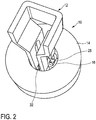
- Fig. 2 shows the direct plug-in arrangement 10 of FIG Fig. 1 from diagonally above.
- Two contact sections 28, 32 can be seen in sections within the through opening 16 of the printed circuit board 14, the structure of which will be explained below.
- Fig. 3 shows the contact 12 in a view obliquely from above.
- the two connection sections 20, 22 which start from the connection section 18 can now be seen.
- the connecting section 22 has two strips 22a, 22b, the strip 22a being connected to the contact section 32 and the strip 22b to the contact section 30.
- the connecting section 20 has two strips 20a, 20b, the strip 20a being connected to the contact section 28 and the strip 20b being connected to the contact section 34.
- An insertion section 36, 38, 40 and 42 each adjoins the contact sections 28 to 34.
- the insertion sections 36, 42 are arranged in the same plane and in alignment with one another and the insertion sections 38, 40 are arranged in the same plane and in alignment with one another.
- the insertion sections 36, 40 are roughly hook-shaped and longer than the insertion sections 38, 42.
- the geometric shapes of the insertion sections 36, 42 and those of the identical insertion sections 38, 40 correspond to the usual design of so-called SKEDD contacts and allow the safe insertion of the Contacts 12 into the through opening 16.
- the contact 12 is made from a sheet metal material, the sheet metal material being stamped and bent. Both the connection section 18, the connection sections 20 and 22, the contact sections 28 to 34 and the connection sections 36 to 42 are thus formed from strips of sheet-like sheet metal.
- the connecting section 20, starting from the connecting section 18, is still designed as a single sheet-metal strip, but then divides into two strips 20a, 20b. Each of these strips 20a, 20b is then connected to a contact section 28, 34.
- the connecting section 22 adjoining the connecting section 18 is initially designed as a sheet metal strip, but then divides into two Strips 22a, 22b. The strip 22a is connected to the contact portion 32 and the strip 22b is connected to the contact portion 30.
- the front and back are larger in area than the side edges.
- the strip 20a is in Fig. 3 only the right side edge and the back can be seen.
- On the strip 22a is in Fiig. 3 the front and the right side edge can be seen.
- the strip 22b is in Fig. 3 only the front and the right side edge can be seen.
- On strip 20b is in Fig. 3 only the back can be seen.
- the rear sides of the strips 20a and 22b or 20b and 22a face one another.
- a first bending point 44a is provided at the transition between the connecting section 20 and the contact section 34, in which the strip 20 is twisted by approximately 45 °.
- the sheet metal strip in the contact section 28 is thus bent by 45 ° with respect to the strip in the connecting section 20.
- the contact section 28 is followed by a second bending point 46a in which the strip is twisted again.
- the angle by which the strip is twisted at the second bending point 46a is of the same magnitude, but opposite to the angle by which the strip is twisted at the first bending point 44a.
- the insertion section 36 which follows the contact section 28, is again arranged in the same plane as the strip 20a in the connecting section.
- the strip is arranged at an angle to the strip 20a in the connecting section 20 and in the insertion section 36.
- the angle by which the strip in the contact section 28 is twisted with respect to the connecting section 20 and the insertion section 36 is approximately 45 ° in the illustrated embodiment and can be between 35 ° and 55 ° within the scope of the invention.
- the contact section 28 is provided with a bulge 48a on its front side.
- This bulge is convex.
- the bulge serves to contact the inner wall of the through opening 16 in the circuit board 14. Due to the convex shape of the bulge 48a, electrically very reliable contact can be made between the convex bulge 48a and the inside of the through opening 16. Between the convex bulge 48a and the inside of the through opening 16 there can be a point-like, line-like or planar contact, a planar contact being preferred.
- the strip 20b is provided with a bending point 44d, in which the strip 20b, before it merges into the contact section 34, is twisted by an angle, approximately 45 °.
- a second bending point 46d leads this twist back again, so that the insertion section 42 is arranged in the same plane and in alignment with the strip 20b of the connecting section 20.
- the connecting section 22 with the strips 22a, 22b is also formed in the same way.
- the contact sections 28, 30 are each twisted by approximately 45 ° with respect to the strips 22a and 22b, and the insertion sections 38, 40 are then each again arranged in a common plane and in alignment with the strips 22a and 22b.
- Each of the contact sections 28 to 34 has a convex bulge 48a, 48b, 48c, 48d. Each of the contact sections 28 to 34 can thereby ensure reliable electrical contact with the inner wall of the through opening 16 in the area of the convex bulge.
- the representation of the Fig. 4 shows enlarged and in sections the contact 12 of FIG Fig. 3 with the strip 20a of the connecting section 20, the bending point 44a adjoining the strip 20a, the contact section 28 following the bending point 44a, the bending point 46a following the contact section 28 and the insertion section 36 following the bending point 46a its lower end has a curved shape and enables the contact 12 to be introduced into the through opening 16 of the circuit board 14.
- the contact section 34 follows the bending point 44d.
- the contact section 34 is followed by a bending point 46d.
- the bending point 46d is followed by the insertion section 38, which is shorter than the opposite insertion section 36 but is rounded at its lower end in order to enable the contact 12 to be inserted into the through opening 14 of the circuit board 16.
- the strip 20a, the bending point 44a, the contact section 28, the bending point 46a and the insertion section 36 consist of a single strip of sheet metal material that was twisted by approximately 45 ° in the area of the bending points 44a, 46a. It can also be seen that this strip of sheet metal material is used in all of the described and in Fig. 4 Sections shown each have two side edges, a front side 50 and a rear side 52. The front side 50 and the rear side 52 have been designated in the area of the contact section 28.
- the Contact section 34 has the bulge 48 a, which is arranged on the front side 50.
- a recess 54a is provided on the opposite rear side 52.
- the bulge 48a is formed as an impression and the depression 54a is formed as an impression. The bulge 48a is thus created when the impression 54a is impressed, for example by pressing a pressing tool from the rear side 52 into the rear side 52.
- the contact portion 34 in Fig. 4 can only be seen from its rear side 56.
- the depression 54d embodied as an impression can be seen here.
- the edge of the recess 54d is still arranged at a small distance from the side edges 60 and 62 of the contact section 28.
- the opposite bulge or embossing is designed such that its edge is at a small distance from the side edges 60, 62 of the contact section 28.
- the recess 54a and the bulge 48a are formed on the contact section 28. Since the edge of the bulge 48a is at a distance from the side edges of the contact section 34, the side edges themselves are not deformed at the same time.
- a pretreated material can be used for the strip of sheet metal material from which the contact 12 is made, for example a galvanized sheet metal material.
- all punched edges are then blank, for example the side edges 60, 62 on the in Fig. 4 left strip 20b and the side edges on the in Fig. 4 right strip 20a, in particular no longer galvanized.
- the side edges 60, 62 extend the entire length of the strip 20b. In addition, all other punched edges are also no longer pretreated.
- the bulge 48a the outer surface of which forms the contact surface with the inner wall of the through opening 14 in the circuit board 16, but still carries the pretreatment layer, for example the electroplating. Any corrosion of the side edges does not affect the electrical properties of the contact between the bulge 48a and the inner wall of the through opening 16 of the circuit board 14. Subsequent treatment of the finished contact 12, for example by means of electroplating, can thus be omitted. The production costs of the contact 12 can be reduced considerably as a result.
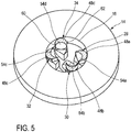
- Fig. 5 shows a sectional view of the direct plug connection of FIG Fig. 1 from obliquely above, a section plane being arranged parallel to the circuit board 14 and approximately halfway up the circuit board 14.
- the cutting plane runs through the contact sections 28, 30, 32, 34 of the contact 12, cf. Fig. 3 . It is in Fig. 5 it can be seen that the bulge 48a of the contact portion 28, the bulge 48b of the contact portion 30, the bulge 48c of the contact portion 22 and the bulge 48d of the contact section 34 rest against the inside of the through opening 16 of the circuit board 14.
- the bulges 48a to 48d are each formed as an embossed area and were created by pressing in the depressions 54a to 54d. Both the bulges 48a to 48d and the depressions 54a to 54d are each shaped like a spherical segment and are formed in that a spherical segment-shaped punch is pressed into the respective rear side of the contact segments 34, 32, 30 and 28, respectively.
- the bulges can also be elongated or flat in sections. How was executed and how in Fig. 5 can be seen, there is a small distance between the side edges of the respective contact section and the edge of the respective bulge, in Fig. 5 recognizable by a small paragraph between the respective side edge and the border of the respective bulge.
- FIG Fig. 5 denoted by the reference numerals 60 and 62 and between the end of the side edges 60, 62 and the beginning of the bulge 48d is shown in FIG Fig. 5 a small paragraph can be seen in each case.
- Fig. 5 also shows that the bulges 48a to 48d are arranged in such a way that at least one point of the bulges 48a to 48d lies on a common circumference, which is in the inserted state of the Fig. 5 is determined by the inner wall of the through opening 16 of the circuit board 14. Even in the relaxed, unplugged state of the contact 12, as shown in FIG Fig. 3 is shown, the bulges 48a to 48d are arranged such that at least one point of the bulges 48a to 48d lies on a common circumference. The apex of the bulges 48a to 48d is advantageously located on a common circumference.
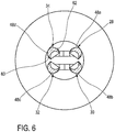
- Fig. 6 shows the sectional view of Fig. 5 in a top view.
- the steps between the side edges 60, 62 of the contact section 34 and the edge of the bulge 48d can be seen in the example of the contact section 34.
- the bulges 48a to 48d do not rest with their apex on the inner wall of the through opening 16 of the printed circuit board 14, but are slightly offset to the side.
- the twist angle by which the contact sections 28, 30, 32 and 34 are twisted can be selected to be smaller than if the contact were to take place at the respective vertex.
- the contact 12 for a direct connection can be produced much more cheaply than conventional contacts, without adversely affecting the functional reliability, since the contact 12 can be produced from pretreated sheet metal material, for example galvanized sheet metal material. This can be done by punching, bending and embossing processes. A Subsequent electroplating of the finished contact 12 is no longer necessary, however, since the electrical contact is produced by means of the bulges 48a to 48d which are pressed out of a flat surface, typically the front side of the pretreated sheet metal material.
Landscapes
- Coupling Device And Connection With Printed Circuit (AREA)
Description
- Die Erfindung betrifft einen Kontakt für eine Direktsteckverbindung mit einem Anschlussabschnitt zum Anschließen einer Kabellitze und einem Kontaktabschnitt zum Herstellen eines elektrischen Kontakts mit einer Durchgangsbohrung einer Leiterplatte und einem, ein freies Ende des Kontakts bildenden Einführabschnitt, wobei der Kontaktabschnitt und der Einführabschnitt an einem Streifen flächigen Blechmaterials mit zwei Seitenkanten, einer Vorderseite und einer Rückseite ausgebildet sind. Die Erfindung betrifft auch eine Direktsteckverbindung mit wenigstens einem Stecker und einer Leiterplatte, wobei die Leiterplatte wenigstens eine Durchgangsöffnung aufweist, die an der Innenseite elektrisch leitfähig ausgebildet ist.
- Aus der internationalen Offenlegungsschrift
WO 2011/155380 A1 ist ein Kontakt bekannt, der einen Streifen flächigen Blechmaterials aufweist, wobei der Streifen über seine gesamte Breite gebogen ist und dadurch eine Auswölbung bildet. - Aus der US-Offenlegungsschrift
US 2007/0010139 A1 ist ein Kontakt für eine Direktsteckverbindung bekannt, der einstückig ausgebildet ist, wobei ein Streifen flächigen Blechmaterials mit einer zentralen Ausnehmung versehen und dann verdrillt worden ist. Der verdrillte Bereich wird dann für eine Kontaktierung einer Durchgangsbohrung einer Leiterplatte genutzt. - Aus der deutschen Offenlegungsschrift
DE 103 25 134 A1 ist ein Kontakt für eine Direktsteckverbindung gemäss dem Oberbegriff des Anspruchs 1 bekannt, wobei der Kontakt in dem Bereich, der für die Kontaktierung einer Durchgangsbohrung einer Leiterplatte vorgesehen ist, eine hohlzylindrische Ausbildung aufweist. Die hohlzylindrische Ausbildung entsteht durch Aufeinanderlegen zweier Halbzylinder, die jeweils durch Auswölben eines Blechstreifens gebildet sind. - Aus der europäischen Offenlegungsschrift
EP 2 105 995 A1 ist eine Kontaktausbildung bekannt, die eine Ausprägung an einem Kontaktstreifen aufweist. Die Auswölbung ist zum mechanischen Festlegen einer Position des Kontaktstreifens in einem nicht leitenden Gehäuse vorgesehen. - Mit der Erfindung sollen ein Kontakt für eine Direktsteckverbindung und eine Direktsteckverbindung verbessert werden.
- Erfindungsgemäß ist hierzu ein Kontakt mit den Merkmalen von Anspruch 1 und eine Direktsteckverbindung mit den Merkmalen von Anspruch 13 vorgesehen.
- Der erfindungsgemäße Kontakt betrifft eine Direktsteckverbindung mit einem Anschlussabschnitt zum Anschließen einer Kabellitze und einem Kontaktabschnitt zum Herstellen eines elektrischen Kontakts mit einer Durchgangsbohrung einer Leiterplatte und einem, ein freies Ende des Kontakts bildenden Einführabschnitt, wobei der Kontaktabschnitt und der Einführabschnitt an einem Streifen flächigen Blechmaterials mit zwei Seitenkanten, einer Vorderseite und einer Rückseite ausgebildet sind, wobei der Streifen im Kontaktabschnitt auf der Vorderseite oder der Rückseite eine konvexe Auswölbung zur Anlage an der Innenseite der Durchgangsöffnung aufweist.
- Indem der Streifen eine konvexe Auswölbung zur Anlage an der Innenseite der Durchgangsöffnung aufweist, kann die Fläche eines Kontaktbereichs mit der Innenseite der Durchgangsöffnung einer Leiterplatte vergrößert werden. Vor allem ist es möglich, galvanisiertes Rohmaterial zu verarbeiten, da eine weitere Nachbearbeitung, speziell eine Nachbearbeitung durch Galvanisieren, entfällt. Der Kontakt kann für eine sogenannte SKEDD-Direktsteckverbindung in besonders vorteilhafter Weise eingesetzt werden. Durch die Verwendung von vorbehandeltem Blechmaterial, beispielsweise galvanisiertem Blechmaterial, können die Herstellkosten wesentlich gesenkt werden, da eine Nachbehandlung, beispielsweise eine galvanische Nachbehandlung, der bezüglich ihrer Geometrie fertiggestellten Kontakte entfallen kann.
- Die konvexe Auswölbung kann in beliebiger Weise gestaltet sein, beispielsweise als Kugelabschnitt, ovale Ausbildung, Freiformfläche oder dergleichen. Die konvexe Auswölbung ist so gestaltet, dass sich ein punktförmiger, linienförmiger oder flächenförmiger Kontakt mit der Innenseite der Durchgangsöffnung der Leiterplatte ergibt. Flächenförmige Kontakte ergeben sich, wenn die Radien der Durchgangsöffnung in der Leiterplatte und der konvexen Auswölbung annähernd gleich sind, bevorzugt gleich sind.
- Gemäß der Erfindung ist die konvexe Auswölbung von den Seitenkanten des Streifens beabstandet.
- Auf diese Weise können vorbehandelte oder vorbeschichtete Blechmaterialien in besonders vorteilhafter Weise eingesetzt werden. Speziell ist nicht zu befürchten, dass beim Herstellen der konvexen Auswölbung nach dem Stanzen die zwangsläufig nicht beschichteten Seitenkanten in den Bereich der konvexen Auswölbung und damit in den Bereich gelangen, der für die Kontaktierung der Innenwand der Durchgangsöffnung in der Leiterplatte vorgesehen ist.
- In Weiterbildung der Erfindung ist die konvexe Auswölbung auf der Vorderseite des Streifens angeordnet und eine konkave Vertiefung ist auf der Rückseite des Streifens, gegenüber der konvexen Auswölbung, angeordnet.
- Auf diese Weise lässt sich die konvexe Auswölbung in besonders einfacher Weise realisieren.
- In Weiterbildung der Erfindung ist die konkave Vertiefung als Einprägung und die konvexe Auswölbung als Ausprägung ausgebildet.
- Durch einen einfachen Prägevorgang lässt sich dadurch in sehr einfacher und prozesssicherer Weise die konvexe Auswölbung herstellen.
- Gemäß der Erfindung ist zwischen dem Anschlussabschnitt und dem Kontaktabschnitt ein Verbindungsabschnitt angeordnet, wobei der Verbindungsabschnitt, der Kontaktabschnitt und der Einführabschnitt aus einem Streifen flächigen Blechmaterials ausgebildet sind und wobei der Streifen zwischen dem Verbindungsabschnitt und dem Kontaktabschnitt eine erste Biegestelle aufweist, an der der Streifen verdrillt ist.
- Durch eine Verdrillung, also eine Biegung um die Längsachse des Streifens zwischen dem Verbindungsabschnitt und dem Kontaktabschnitt, kann die konvexe Auswölbung im Kontaktabschnitt so angeordnet werden, dass sie beim Einstecken des Kontakts in eine Durchgangsöffnung einer Leiterplatte zuverlässig mit der Innenwand der Durchgangsöffnung in Kontakt kommt.
- In Weiterbildung der Erfindung weist der Streifen zwischen dem Kontaktabschnitt und dem Einführabschnitt eine zweite Biegestelle auf, an der der Streifen verdrillt ist.
- Auf diese Weise kann der Einführabschnitt so angeordnet werden, dass er die ihm zugedachte Funktion, also das sichere Einführen des Kontakts in die Durchgangsöffnung der Leiterplatte zu ermöglichen, zuverlässig erfüllen kann.
- In Weiterbildung der Erfindung sind die Verdrillungen, also die Biegungen um die Längsachse des Streifens, an der ersten Biegestelle und an der zweiten Biegestelle so ausgebildet, dass der Verbindungsabschnitt des Streifens und der Einführabschnitt des Streifens fluchtend zueinander ausgerichtet sind.
- Auf diese Weise kann also lediglich der Kontaktabschnitt im Winkel zum Verbindungsabschnitt und zum Einführabschnitt angeordnet werden, um eine optimale Position des Kontaktabschnitts und vor allem der konvexen Auswölbung zu erzielen, so dass die konvexe Auswölbung nach dem Einführen des Kontakts in eine Durchgangsöffnung einer Leiterplatte einen sicheren elektrischen Kontakt mit der Innenwand der Durchgangsöffnung herstellen kann.
- In Weiterbildung der Erfindung beträgt der Verdrillungswinkel an der ersten Biegestelle und/oder der zweiten Biegestelle im Bereich zwischen 35° und 55°, insbesondere 45°.
- In Weiterbildung der Erfindung sind im Kontaktabschnitt und im Einführabschnitt jeweils wenigstens vier Streifen aus flächigem Blechmaterial vorgesehen, wobei im Einführabschnitt jeweils zwei Streifen in einer gemeinsamen Ebene angeordnet sind und alle Streifen im Kontaktabschnitt eine konvexe Auswölbung aufweisen.
- Durch vier Streifen lässt sich die Kontaktfläche noch weiter vergrößern.
- In Weiterbildung der Erfindung sind die konvexen Auswölbungen jeweils so ausgerichtet, dass im Querschnitt gesehen wenigstens ein Punkt jeder konvexen Auswölbung einen gemeinsamen, gedachten Umkreis berührt.
- Im Falle einer kreisförmigen Durchgangsöffnung in einer Leiterplatte kann dadurch eine optimale Kontaktgabe der konvexen Auswölbungen mit der Innenseite der Durchgangsöffnung realisiert werden.
- In Weiterbildung der Erfindung berühren im Querschnitt gesehen die Scheitelpunkte aller konvexen Auswölbungen einen gemeinsamen, gedachten Umkreis.
- Das der Erfindung zugrunde liegende Problem wird auch durch eine Direktsteckverbindung mit wenigstens einem Stecker und einer Leiterplatte gelöst, wobei die Leiterplatte wenigstens eine Durchgangsöffnung aufweist, die an der Innenseite elektrisch leitfähig ausgebildet ist, und wobei der Stecker wenigstens einen erfindungsgemäßen Kontakt aufweist und der Kontakt des Steckers in die Durchgangsöffnung der Leiterplatte eingesteckt ist, bei der der Kontakt die Innenwand der Durchgangsöffnung mit der konvexen Auswölbung berührt.
- Weitere Merkmale und Vorteile der Erfindung ergeben sich aus den Ansprüchen und der nachfolgenden Beschreibung bevorzugter Ausführungsformen der Erfindung im Zusammenhang mit den Zeichnungen. Einzelmerkmale der unterschiedlichen, dargestellten Ausführungsformen lassen sich dabei in beliebiger Weise miteinander kombinieren, ohne den Rahmen der Erfindung zu überschreiten. In den Zeichnungen zeigen:
- Fig. 1
- eine Ansicht einer erfindungsgemäßen Direktsteckverbindung mit einem Kontakt und einer abschnittsweise dargestellten Leiterplatte von schräg oben,
- Fig. 2
- eine weitere Ansicht der Direktsteckverbindung der
Fig. 1 von schräg oben, - Fig. 3
- den Kontakt der Direktsteckverbindung der
Fig. 1 und2 von schräg vorne, - Fig. 4
- eine abschnittsweise Darstellung des Kontakts der
Fig. 3 im Bereich zweier Kontaktabschnitte, - Fig. 5
- eine Schnittansicht der Direktsteckverbindung der
Fig. 2 und - Fig. 6
- die Schnittansicht der
Fig. 5 aus einem anderen Winkel. -
Fig. 1 zeigt eine erfindungsgemäße Direktsteckverbindung 10 mit einem Kontakt 12 und einer lediglich abschnittsweise dargestellten Leiterplatte 14. Die Leiterplatte 14 ist lediglich im Bereich einer Durchgangsöffnung 16 dargestellt. In nicht zu erkennender Weise ist die Durchgangsöffnung 16 auf ihrer Innenwand elektrisch leitfähig ausgeführt und die elektrisch leitfähige Innenwand ist in ebenfalls nicht dargestellter Weise mit Leiterbahnen an der Leiterplatte 14 elektrisch verbunden. Mittels des Kontakts 12 kann damit ein elektrischer Kontakt mit den Leiterbahnen der Leiterplatte 14 hergestellt werden. Der Kontakt 12 kann entweder als Einzelkontakt ausgebildet sein oder Teil eines Einfachsteckers oder eines Mehrfachsteckers bilden. In beiden Fällen ist der Kontakt 12 in einem nicht dargestellten Gehäuse aufgenommen und mit einer ebenfalls nicht dargestellten Kabellitze verbunden. Im Falle eines Mehrfachsteckers sind mehrere der Kontakte 12 nebeneinander in einem Gehäuse angeordnet und jedem der Kontakte 12 ist dann eine separate Durchgangsöffnung 16 in der Leiterplatte 14 zugeordnet. - Der Kontakt 12 weist einen Anschlussabschnitt 18 zum Anschließen einer Kabellitze auf. Der Anschlussabschnitt 18 ist lediglich schematisch dargestellt und kann beispielsweise als Schneidklemmkontakt oder als Crimpkontakt ausgebildet sein. An den Anschlussabschnitt 18 schließen sich zwei Verbindungsabschnitte 20, 22 an, die den Anschlussabschnitt 18 mit jeweils zwei, in
Fig. 1 nicht erkennbaren Kontaktabschnitten verbinden. Die Kontaktabschnitte sind in der Darstellung derFig. 1 durch die Leiterplatte 14 verdeckt. - In
Fig. 1 sind unterhalb der Leiterplatte 14 noch zwei Einführabschnitte 24, 26 zu erkennen, die ein Einführen des Kontakts 12 in die Durchgangsöffnung 16 ermöglichen und die nachfolgend noch detaillierter erläutert werden. -
Fig. 2 zeigt die Direktsteckanordnung 10 derFig. 1 von schräg oben. Innerhalb der Durchgangsöffnung 16 der Leiterplatte 14 sind abschnittsweise zwei Kontaktabschnitte 28, 32 zu erkennen, deren Aufbau nachfolgend noch erläutert wird. -
Fig. 3 zeigt den Kontakt 12 in einer Ansicht von schräg oben. Zu erkennen sind nun die beiden Verbindungsabschnitte 20, 22, die von dem Anschlussabschnitt 18 ausgehen. Der Verbindungsabschnitt 22 weist zwei Streifen 22a, 22b auf, wobei der Streifen 22a mit dem Kontaktabschnitt 32 und der Streifen 22b mit dem Kontaktabschnitt 30 verbunden ist. Der Verbindungsabschnitt 20 weist zwei Streifen 20a, 20b auf, wobei der Streifen 20a mit dem Kontaktabschnitt 28 und der Streifen 20b mit dem Kontaktabschnitt 34 verbunden ist.. - An die Kontaktabschnitte 28 bis 34 schließt sich jeweils ein Einführabschnitt 36, 38, 40 und 42 an. Die Einführabschnitte 36, 42 sind in der gleichen Ebene und zueinander fluchtend angeordnet und die Einführabschnitte 38, 40 sind in der gleichen Ebene und zueinander fluchtend angeordnet. Die Einführabschnitte 36, 40 sind etwa hakenförmig ausgebildet und länger als die Einführabschnitte 38, 42. Die geometrischen Formen der Einführabschnitte 36, 42 und die der gleich ausgeführten Einführabschnitte 38, 40 entsprechen der üblichen Gestaltung von sogenannten SKEDD-Kontakten und erlauben das sichere Einführen des Kontakts 12 in die Durchgangsöffnung 16.
- Der Kontakt 12 ist aus einem Blechmaterial hergestellt, wobei das Blechmaterial gestanzt und gebogen wird. Sowohl der Anschlussabschnitt 18, die Verbindungsabschnitte 20 und 22, die Kontaktabschnitte 28 bis 34 und die Verbindungsabschnitte 36 bis 42 sind somit aus Streifen flächigen Blechmaterials gebildet. Der Verbindungsabschnitt 20 ist ausgehend vom Anschlussabschnitt 18 noch als einziger Blechstreifen ausgebildet, teilt sich dann aber in zwei Streifen 20a, 20b. Jeder dieser Streifen 20a, 20b ist dann mit einem Kontaktabschnitt 28, 34 verbunden. In gleicher Weise ist der Verbindungsabschnitt 22 anschließend an den Anschlussabschnitt 18 zunächst als ein Blechstreifen ausgebildet, teilt sich dann aber in zwei Streifen 22a, 22b. Der Streifen 22a ist mit dem Kontaktabschnitt 32 verbunden und der Streifen 22b ist mit dem Kontaktabschnitt 30 verbunden.
- Die Streifen 20a, 20b, 22a, 22b sowie die ebenfalls jeweils aus der Fortsetzung des jeweiligen Streifens 20a, 20b, 22a, 22b bestehenden Kontaktabschnitte 28 bis 34 und Einführabschnitte 36 bis 42 weisen jeweils eine Vorderseite, eine Rückseite und zwei Seitenkanten auf. Die Vorderseite und Rückseite sind gegenüber den Seitenkanten flächenmäßig größer. Am Streifen 20a ist in
Fig. 3 lediglich die rechte Seitenkante und die Rückseite zu erkennen. Am Streifen 22a ist in Fiig. 3 die Vorderseite und die rechte Seitenkante zu erkennen. Am Streifen 22b ist inFig. 3 lediglich die Vorderseite und die rechte Seitenkante zu erkennen. Am Streifen 20b ist inFig. 3 lediglich die Rückseite zu erkennen. Die Rückseiten der Streifen 20a und 22b beziehungsweise 20b und 22a sind einander zugewandt. -
Fig. 3 lässt erkennen, dass am Übergang zwischen dem Verbindungsabschnitt 20 und dem Kontaktabschnitt 34 eine erste Biegestelle 44a vorgesehen ist, in der eine Verdrillung des Streifens 20 um etwa 45° vorgenommen ist. Der Blechstreifen ist im Kontaktabschnitt 28 damit um 45° gegenüber dem Streifen im Verbindungsabschnitt 20 gebogen. Auf den Kontaktabschnitt 28 folgt eine zweite Biegestelle 46a, in der der Streifen wieder verdrillt ist. Der Winkel, um den der Streifen an der zweiten Biegestelle 46a verdrillt wird, ist betragsmäßig genauso groß, aber entgegengesetzt zu dem Winkel, um den der Streifen an der ersten Biegestelle 44a verdrillt wird. Dadurch ist der Einführabschnitt 36, der auf den Kontaktabschnitt 28 folgt, wieder in der gleichen Ebene wie der Streifen 20a im Verbindungsabschnitt angeordnet. Im Kontaktabschnitt 28 ist der Streifen hingegen im Winkel zu dem Streifen 20a im Verbindungsabschnitt 20 und im Einführabschnitt 36 angeordnet. Der Winkel, um den der Streifen im Kontaktabschnitt 28 gegenüber dem Verbindungsabschnitt 20 und dem Einführabschnitt 36 verdrillt ist, beträgt bei der dargestellten Ausführungsform etwa 45° und kann im Rahmen der Erfindung zwischen 35° und 55° liegen.. - In
Fig. 3 ist weiter zu erkennen, dass der Kontaktabschnitt 28 auf seiner Vorderseite mit einer Auswölbung 48a versehen ist. Diese Auswölbung ist konvex ausgebildet. Die Auswölbung dient dazu, die Innenwand der Durchgangsöffnung 16 in der Leiterplatte 14 zu kontaktieren. Durch die konvexe Form der Auswölbung 48akann eine elektrisch sehr zuverlässige Kontaktierung zwischen der konvexen Auswölbung 48a und der Innenseite der Durchgangsöffnung 16 erfolgen. Zwischen der konvexen Auswölbung 48a und der Innenseite der Durchgangsöffnung 16 kann ein punktförmiger, linienförmiger oder flächenförmiger Kontakt vorliegen, wobei ein flächenförmiger Kontakt bevorzugt ist. - Der Streifen 20b ist mit einer Biegestelle 44d versehen, in der der Streifen 20b, bevor er in den Kontaktabschnitt 34 übergeht, um einen Winkel, etwa 45°, verdrillt ist. Eine zweite Biegestelle 46d führt diese Verdrillung wieder zurück, so dass der Einführabschnitt 42 in der gleichen Ebene und fluchtend zu dem Streifen 20b des Verbindungsabschnitts 20 angeordnet ist.
- In gleicher Weise ist auch der Verbindungsabschnitt 22 mit den Streifen 22a, 22b ausgebildet. Die Kontaktabschnitte 28, 30 sind jeweils um etwa 45° gegenüber den Streifen 22a bzw. 22b verdrillt und die Einführabschnitte 38, 40 sind dann jeweils wieder in einer gemeinsamen Ebene und fluchtend zu den Streifen 22a bzw. 22b angeordnet.
- Jeder der Kontaktabschnitte 28 bis 34 weist eine konvexe Auswölbung 48a, 48b, 48c, 48d auf. Jeder der Kontaktabschnitte 28 bis 34 kann dadurch im Bereich der konvexen Auswölbung für einen zuverlässigen elektrischen Kontakt mit der Innenwand der Durchgangsöffnung 16 sorgen.
- Die Darstellung der
Fig. 4 zeigt vergrößert und abschnittsweise den Kontakt 12 derFig. 3 mit dem Streifen 20a des Verbindungsabschnitts 20, der sich an den Streifen 20a anschließenden Biegestelle 44a, dem auf die Biegestelle 44a folgenden Kontaktabschnitt 28, der auf den Kontaktabschnitt 28 folgenden Biegestelle 46a und dem auf die Biegestelle 46a folgenden Einführabschnitt 36. Der Einführabschnitt 36 weist an seinem unteren Ende eine gekrümmte Form auf und ermöglicht das Einführen des Kontakts 12 in die Durchgangsöffnung 16 der Leiterplatte 14. - In der gleichen Ebene wie die eben beschriebenen Elemente des Kontakts liegt der Streifen 22b des Verbindungsabschnitts 20, auf den eine Biegestelle 44d folgt. Auf die Biegestelle 44d folgt der Kontaktabschnitt 34. Auf den Kontaktabschnitt 34 folgt eine Biegestelle 46d. Auf die Biegestelle 46d folgt dann der Einführabschnitt 38, der kürzer ist als der gegenüberliegende Einführabschnitt 36, aber an seinem unteren Ende abgerundet ausgebildet ist, um das Einführen des Kontakts 12 in die Durchgangsöffnung 14 der Leiterplatte 16 zu ermöglichen.
- Es ist zu erkennen, dass der Streifen 20a, die Biegestelle 44a, der Kontaktabschnitt 28, die Biegestelle 46a und der Einführabschnitt 36 aus einem einzigen Streifen aus flächigem Blechmaterial bestehen, der im Bereich der Biegestellen 44a, 46a um jeweils etwa 45° verdrillt wurde. Es ist auch zu erkennen, dass dieser Streifen aus Blechmaterial in allen beschriebenen und in
Fig. 4 dargestellten Abschnitten jeweils zwei Seitenkanten, eine Vorderseite 50 und eine Rückseite 52 aufweist. Die Vorderseite 50 und die Rückseite 52 wurden im Bereich des Kontaktabschnitts 28 bezeichnet. Bei der dargestellten Ausführungsform weist der Kontaktabschnitt 34 die Auswölbung 48a auf, die auf der Vorderseite 50 angeordnet ist. Auf der gegenüberliegenden Rückseite 52 ist eine Vertiefung 54a vorgesehen. Die Auswölbung 48a ist als Ausprägung und die Vertiefung 54a ist als Einprägung ausgebildet. Die Auswölbung 48a entsteht somit beim Einprägen der Einprägung 54a, indem beispielsweise ein Presswerkzeug von der Rückseite 52 her in die Rückseite 52 eingedrückt wird. - Der Kontaktabschnitt 34 in
Fig. 4 ist lediglich von seiner Rückseite 56 her zu erkennen. Infolgedessen ist hier lediglich die als Einprägung ausgebildete Vertiefung 54d zu erkennen. Anhand der Vertiefung 54d ist zu erkennen, dass die Berandung der Vertiefung 54d noch in einem kleinen Abstand zu den Seitenkanten 60 bzw. 62 des Kontaktabschnitts 28 angeordnet ist. In gleicher Weise ist die gegenüberliegende Auswölbung bzw. Ausprägung so ausgebildet, dass ihre Berandung in einem geringen Abstand von den Seitenkanten 60, 62 des Kontaktabschnitts 28 liegt. In gleicher Weise sind die Vertiefung 54a und die Auswölbung 48a am Kontaktabschnitt 28 ausgebildet. Da die Berandung der Auswölbung 48a einen Abstand von den Seitenkanten des Kontaktabschnitts 34 hat, werden die Seitenkanten selbst nicht mitverformt. Die Auswölbung 48a wird also lediglich aus der Vorderseite 50 des Kontaktabschnitts 28 herausgedrückt. Dadurch kann für den Streifen flächigen Blechmaterials, aus dem der Kontakt 12 hergestellt wird, ein vorbehandeltes Material verwendet werden, beispielsweise ein galvanisiertes flächiges Blechmaterial. Nach dem Ausstanzen sind dann alle Stanzkanten blank, beispielsweise die Seitenkanten 60, 62 an dem inFig. 4 linken Streifen 20b und die Seitenkanten an dem inFig. 4 rechten Streifen 20a , insbesondere nicht mehr galvanisiert. Die Seitenkanten 60, 62 erstrecken sich über die gesamte Länge des Streifens 20b. Darüber hinaus sind alle weiteren Stanzkanten ebenfalls nicht mehr vorbehandelt. Die Auswölbung 48a, deren Außenfläche ja die Kontaktfläche zur Innenwand der Durchgangsöffnung 14 in der Leiterplatte 16 bildet, trägt aber noch die Vorbehandlungsschicht, beispielsweise die Galvanisierung. Eine eventuelle Korrosion der Seitenkanten beeinflusst dadurch die elektrischen Eigenschaften des Kontakts zwischen der Auswölbung 48a und der Innenwand der Durchgangsöffnung 16 der Leiterplatte 14 nicht. Eine nachträgliche Behandlung des fertiggestellten Kontakts 12, beispielsweise mittels Galvanisierung, kann dadurch unterbleiben. Die Herstellungskosten des Kontakts 12 können dadurch erheblich gesenkt werden. -
Fig. 5 zeigt eine Schnittansicht der Direktsteckverbindung derFig. 1 von schräg oben, wobei eine Schnittebene parallel zur Leiterplatte 14 und etwa auf halber Höhe der Leiterplatte 14 angeordnet wurde. Die Schnittebene läuft durch die Kontaktabschnitte 28, 30, 32, 34 des Kontakts 12, vgl.Fig. 3 . Es ist inFig. 5 zu erkennen, dass die Auswölbung 48a des Kontaktabschnitts28, die Auswölbung 48b des Kontaktabschnitts 30, die Auswölbung 48c des Kontaktabschnitts 22 und die Auswölbung 48d des Kontaktabschnitts 34 an der Innenseite der Durchgangsöffnung 16 der Leiterplatte 14 anliegen. Wie bereits ausgeführt wurde und wie inFig. 5 gut zu erkennen ist, sind die Auswölbungen 48a bis 48d jeweils als Ausprägungen ausgebildet und sind entstanden durch Einpressen der Vertiefungen 54a bis 54d. Sowohl die Auswölbungen 48a bis 48d als auch die Vertiefungen 54a bis 54d sind jeweils kugelabschnittsförmig und werden dadurch ausgebildet, dass ein kugelabschnittsförmiger Stempel in die jeweilige Rückseite der Kontaktabschnitte 34, 32, 30 bzw. 28 eingepresst wird. Die Auswölbungen können auch länglich oder abschnittsweise flächig ausgebildet sein. Wie ausgeführt wurde und wie inFig. 5 zu erkennen ist, liegt zwischen den Seitenkanten des jeweiligen Kontaktabschnitts und dem Rand der jeweiligen Auswölbung ein kleiner Abstand, inFig. 5 zu erkennen durch jeweils einen kleinen Absatz zwischen der jeweiligen Seitenkante und der Berandung der jeweiligen Auswölbung. Anhand des Kontaktabschnitts 34 sind die beiden Seitenkanten inFig. 5 mit den Bezugsziffern 60 bzw. 62 bezeichnet und zwischen dem Ende der Seitenkanten 60, 62 und dem Beginn der Auswölbung 48d ist inFig. 5 jeweils ein kleiner Absatz zu erkennen. -
Fig. 5 lässt darüber hinaus erkennen, dass die Auswölbungen 48a bis 48d so angeordnet sind, dass jeweils wenigstens ein Punkt der Auswölbungen 48a bis 48d auf einem gemeinsamen Umkreis liegt, der im eingesteckten Zustand derFig. 5 durch die Innenwand der Durchgangsöffnung 16 der Leiterplatte 14 bestimmt ist. Auch im entspannten, nicht eingesteckten Zustand des Kontakts 12, wie er inFig. 3 dargestellt ist, sind die Auswölbungen 48a bis 48d so angeordnet, dass wenigstens ein Punkt der Auswölbungen 48a bis 48d auf einem gemeinsamen Umkreis liegt. In vorteilhafter Weise liegt der Scheitelpunkt der Auswölbungen 48a bis 48d auf einem gemeinsamen Umkreis. -
Fig. 6 zeigt die Schnittansicht derFig. 5 in einer Ansicht von oben. Zu erkennen sind am Beispiel des Kontaktabschnitts 34 die Absätze zwischen den Seitenkanten 60, 62 des Kontaktabschnitts 34 und der Berandung der Auswölbung 48d. Weiter ist zu erkennen, dass die Auswölbungen 48a bis 48d nicht mit ihrem Scheitelpunkt an der Innenwand der Durchgangsöffnung 16 der Leiterplatte 14 anliegen, sondern leicht seitlich versetzt hierzu. Dadurch kann der Verdrillungswinkel, um den die Kontaktabschnitte 28, 30, 32 und 34 verdrillt sind, kleiner gewählt werden als dann, wenn der Kontakt im jeweiligen Scheitelpunkt erfolgen würde. - Mit der Erfindung lässt sich der Kontakt 12 für eine Direktverbindung wesentlich günstiger herstellen, ohne die Funktionssicherheit negativ zu beeinflussen, als herkömmliche Kontakte, da der Kontakt 12 aus vorbehandeltem Blechmaterial, beispielsweise galvanisiertem Blechmaterial, hergestellt werden kann. Dies kann durch Stanz-, Biege- und Prägevorgänge erfolgen. Eine nachträgliche Galvanisierung des fertiggestellten Kontakts 12 ist aber nicht mehr erforderlich, da der elektrische Kontakt mittels den Auswölbungen 48a bis 48d hergestellt wird, die aus einer ebenen Fläche, typischerweise der Vorderseite des vorbehandelten Blechmaterials, herausgedrückt werden.
Claims (10)
- Kontakt (12) für Direktsteckverbindung (10) mit einem Anschlussabschnitt (18) zum Anschließen einer Kabellitze und einem Kontaktabschnitt (28, 30, 32, 34) zum Herstellen eines elektrischen Kontakts mit einer Durchgangsöffnung (16) einer Leiterplatte (14) und einem, ein freies Ende des Kontakts (12) bildenden Einführabschnitt (36, 38), wobei der Kontaktabschnitt (28, 30, 32, 34) und der Einführabschnitt (36, 38) an einem Streifen (20a, 20b, 22a, 22b) flächigen Blechmaterials mit zwei Seitenkanten (60, 62), einer Vorderseite (50) und einer Rückseite (52) ausgebildet sind, wobei zwischen dem Anschlussabschnitt (18) und dem Kontaktabschnitt (28, 30, 32, 34) ein Verbindungsabschnitt (20, 22) angeordnet ist, wobei der Verbindungsabschnitt (20, 22), der Kontaktabschnitt (28, 30, 32, 34) und der Einführabschnitt (36, 38) aus einem Streifen flächigen Blechmaterials ausgebildet sind und wobei der Streifen (20a, 20b, 22a, 22b) im Kontaktabschnitt (28, 30, 32, 34) auf der Vorderseite (50) oder der Rückseite (52) eine insbesondere konvexe Auswölbung (48a, 48b, 48c, 48d) zur Anlage an der Innenseite der Durchgangsöffnung (16) aufweist, dadurch gekennzeichnet,
dass die Auswölbung (48a, 48b, 48c, 48d) von den Seitenkanten (60, 62) des Streifens (20a, 20b, 22a, 22b) beabstandet ist und wobei der Streifen zwischen dem Verbindungsabschnitt (20, 22) und dem Kontaktabschnitt (28, 30, 32, 34) eine erste Biegestelle (44a, 44b, 44c, 44d) aufweist, an der der Streifen verdrillt ist. - Kontakt nach Anspruch 1, dadurch gekennzeichnet, dass die insbesondere konvexe Auswölbung (48a, 48b, 48c, 48d) auf der Vorderseite (50) des Streifens (20a, 20b, 22a, 22b) angeordnet ist und dass eine insbesondere konkave Vertiefung (54a, 54b, 54c, 54d) auf der Rückseite (52) des Streifens (20a, 20b, 22a, 22b), gegenüber der Auswölbung (48a, 48b, 48c, 48d), angeordnet ist.
- Kontakt nach Anspruch 2, dadurch gekennzeichnet, dass die Vertiefung (54a, 54b, 54c, 54d) als Einprägung und die Auswölbung (48a, 48b, 48c, 48d) als Ausprägung ausgebildet ist.
- Kontakt nach einem der vorstehenden Ansprüche, dadurch gekennzeichnet, dass der Streifen zwischen dem Kontaktabschnitt (28, 30, 32, 34) und dem Einführabschnitt (36, 38) eine zweite Biegestelle (46a, 46b, 46c, 46d) aufweist, an der der Streifen verdrillt ist.
- Kontakt nach Anspruch 4, dadurch gekennzeichnet, dass die Verdrillungen an der ersten Biegestelle (44a, 44b, 44c, 44d) und an der zweiten Biegestelle (46a, 46b, 46c, 46d) so ausgebildet sind, dass der Verbindungsabschnitt (20, 22) des Streifens und der Einführabschnitt (36, 38) des Streifens fluchtend zueinander ausgerichtet ist.
- Kontakt nach einem der Ansprüche 4 oder 5, dadurch gekennzeichnet, dass der Verdrillungswinkel an der ersten Biegestelle (44a, 44b, 44c, 44d) und/oder der zweiten Biegestelle (46a, 46b, 46c, 46d) im Bereich zwischen 35 Winkelgrad und 55 Winkelgrad, insbesondere 45 Winkelgrad, beträgt.
- Kontakt nach wenigstens einem der vorstehenden Ansprüche, dadurch gekennzeichnet, dass im Kontaktabschnitt und im Einführabschnitt jeweils wenigstens vier Streifen aus flächigem Blechmaterial vorgesehen sind, wobei im Einführabschnitt jeweils zwei Streifen in einer gemeinsamen Ebene angeordnet sind und alle Streifen im Kontaktabschnitt eine Auswölbung (48a, 48b, 48c, 48d) aufweisen.
- Kontakt nach Anspruch 7, dadurch gekennzeichnet, dass die konvexen Auswölbungen (48a, 48b, 48c, 48d) jeweils so ausgerichtet sind, dass im Querschnitt gesehen wenigstens ein Punkt von jeder Auswölbung (48a, 48b, 48c, 48d) einen gemeinsamen, gedachten Umkreis berührt.
- Kontakt nach Anspruch 8, dadurch gekennzeichnet, dass im Querschnitt gesehen die Scheitelpunkte aller Auswölbungen (48a, 48b, 48c, 48d) einen gemeinsamen, gedachten Umkreis berühren.
- Direktsteckverbindung (10) mit wenigstens einem Stecker und einer Leiterplatte (14), wobei die Leiterplatte (14) wenigstens eine Durchgangsöffnung (16) aufweist, die an der Innenseite elektrisch leitfähig ausgebildet ist und wobei der Stecker wenigstens einen Kontakt (12) nach wenigstens einem der vorstehenden Ansprüche aufweist und der Kontakt (12) des Steckers in die Durchgangsöffnung der Leiterplatte (14) eingesteckt ist, dadurch gekennzeichnet, dass der Kontakt (12) die Innenwand der Durchgangsöffnung mit der Auswölbung (48a, 48b, 48c, 48d) berührt.
Applications Claiming Priority (1)
| Application Number | Priority Date | Filing Date | Title |
|---|---|---|---|
| DE102018210234.1A DE102018210234B3 (de) | 2018-06-22 | 2018-06-22 | Kontakt für Direktsteckverbindung und Direktsteckverbindung |
Publications (2)
| Publication Number | Publication Date |
|---|---|
| EP3588682A1 EP3588682A1 (de) | 2020-01-01 |
| EP3588682B1 true EP3588682B1 (de) | 2021-04-28 |
Family
ID=66821106
Family Applications (1)
| Application Number | Title | Priority Date | Filing Date |
|---|---|---|---|
| EP19179478.3A Active EP3588682B1 (de) | 2018-06-22 | 2019-06-11 | Kontakt für direktsteckverbindung und direktsteckverbindung |
Country Status (7)
| Country | Link |
|---|---|
| US (1) | US10797415B2 (de) |
| EP (1) | EP3588682B1 (de) |
| JP (1) | JP6841868B2 (de) |
| KR (1) | KR102735280B1 (de) |
| CN (1) | CN110635267B (de) |
| DE (1) | DE102018210234B3 (de) |
| TW (1) | TWI708435B (de) |
Families Citing this family (1)
| Publication number | Priority date | Publication date | Assignee | Title |
|---|---|---|---|---|
| DE102018210237A1 (de) * | 2018-06-22 | 2019-12-24 | Würth Elektronik eiSos Gmbh & Co. KG | Kontakt für Direktsteckverbinder und Direktsteckverbinder |
Family Cites Families (34)
| Publication number | Priority date | Publication date | Assignee | Title |
|---|---|---|---|---|
| US3760340A (en) * | 1971-10-29 | 1973-09-18 | Du Pont | Circuit board socket |
| JPS5135064A (de) * | 1974-09-19 | 1976-03-25 | Nippon Emp Kk | |
| US4260216A (en) * | 1979-08-14 | 1981-04-07 | Universal Instruments Corporation | Spade terminal |
| US4363529A (en) * | 1980-07-25 | 1982-12-14 | Amp Incorporated | Terminal having improved mounting means |
| US4498724A (en) * | 1981-09-18 | 1985-02-12 | Bicc Public Limited Company | Circuit board composite connector |
| US4780958A (en) * | 1986-10-06 | 1988-11-01 | Amp Incorporated | Method of making an electrical terminal for a printed circuit board |
| WO1992005606A1 (de) | 1990-09-24 | 1992-04-02 | Siemens Aktiengesellschaft | Koaxial-steckverbinderelement zur verbindung mit einer leiterplatte |
| US5147227A (en) * | 1991-10-17 | 1992-09-15 | Amp Incorporated | Terminal retention device |
| US5112249A (en) * | 1991-10-18 | 1992-05-12 | Amp Incorporated | Connector locking clip |
| US5374204A (en) * | 1993-11-30 | 1994-12-20 | The Whitake Corporation | Electrical terminal with compliant pin section |
| JP2923518B2 (ja) * | 1994-03-18 | 1999-07-26 | 矢崎総業株式会社 | 大電流用端子及び加工方法 |
| US6080008A (en) * | 1998-05-28 | 2000-06-27 | The Whitaker Corporation | Push-wire contact |
| WO2001059885A2 (en) * | 2000-02-09 | 2001-08-16 | Solid State Stamping, Inc. | Compliant pin and its method of manufacture |
| US6354849B1 (en) * | 2000-10-10 | 2002-03-12 | Hon Hai Precision Ind. Co., Ltd. | Board-engaging structure for contacts of an electrical connector |
| JP2002298962A (ja) | 2001-03-30 | 2002-10-11 | Jst Mfg Co Ltd | 樹脂ハンダを用いた電気接触子、電気コネクタ及びこれらのプリント配線板への接続方法 |
| DE10325134A1 (de) * | 2003-06-04 | 2004-12-23 | Conti Temic Microelectronic Gmbh | Einpresskontakt |
| JP2005129274A (ja) * | 2003-10-21 | 2005-05-19 | Fujitsu Ten Ltd | プレスフィット端子および接続構造 |
| JP2005222821A (ja) * | 2004-02-05 | 2005-08-18 | Auto Network Gijutsu Kenkyusho:Kk | プレスフィット端子 |
| US7377823B2 (en) * | 2005-05-23 | 2008-05-27 | J.S.T. Corporation | Press-fit pin |
| US7249981B2 (en) * | 2005-07-08 | 2007-07-31 | J.S.T. Corporation | Press-fit pin |
| JP2008053091A (ja) * | 2006-08-25 | 2008-03-06 | Honda Tsushin Kogyo Co Ltd | プレスフィットコンタクト |
| ITMI20080513A1 (it) * | 2008-03-27 | 2009-09-28 | Cabur S R L | Dispositivo connettore perfezionato per il collegamento elettrico tra morsetti elettrici, metodo per la realizzazione di tale dispositivo connettore e gruppo di collegamento elettrico dotato di tale dispositivo connettore perfezionato |
| WO2011155380A1 (ja) * | 2010-06-09 | 2011-12-15 | シャープ株式会社 | コネクタ |
| DE102011003809A1 (de) | 2011-02-08 | 2012-08-09 | Robert Bosch Gmbh | Direktsteckverbinder zur elektrischen Direktkontaktierung einer Leiterplatte |
| DE102011005073A1 (de) * | 2011-03-03 | 2012-09-06 | Würth Elektronik Ics Gmbh & Co. Kg | Tandem Multi Fork Einpresspin |
| JP5445605B2 (ja) * | 2011-08-30 | 2014-03-19 | 第一精工株式会社 | プレスフィット用コネクタ端子 |
| US8902605B2 (en) * | 2012-06-13 | 2014-12-02 | International Business Machines Corporation | Adapter for plated through hole mounting of surface mount component |
| US9362630B2 (en) * | 2012-11-27 | 2016-06-07 | Molex, Llc | Wire to board terminal |
| US9300069B2 (en) * | 2014-02-13 | 2016-03-29 | Delphi Technologies, Inc. | Electrical terminal with enhanced clamping force |
| DE102015110070A1 (de) * | 2015-06-23 | 2016-12-29 | Johnson Electric S.A. | Elektrische Verbindungsanordnung |
| CN204927573U (zh) | 2015-08-07 | 2015-12-30 | 浙江绍兴苏泊尔生活电器有限公司 | 线路板直插结构和食物料理机 |
| DE102015119478A1 (de) * | 2015-11-11 | 2017-05-11 | Phoenix Contact Gmbh & Co. Kg | Elektrische Anschlussklemme |
| DE202016008242U1 (de) | 2016-04-22 | 2017-05-10 | Phoenix Contact Gmbh & Co. Kg | Steckkontakt |
| DE102016107482A1 (de) * | 2016-04-22 | 2017-10-26 | Phoenix Contact Gmbh & Co. Kg | Steckkontakt |
-
2018
- 2018-06-22 DE DE102018210234.1A patent/DE102018210234B3/de active Active
-
2019
- 2019-06-11 EP EP19179478.3A patent/EP3588682B1/de active Active
- 2019-06-18 US US16/444,247 patent/US10797415B2/en active Active
- 2019-06-19 KR KR1020190073126A patent/KR102735280B1/ko active Active
- 2019-06-21 JP JP2019115544A patent/JP6841868B2/ja active Active
- 2019-06-21 CN CN201910542168.8A patent/CN110635267B/zh active Active
- 2019-06-21 TW TW108121703A patent/TWI708435B/zh active
Non-Patent Citations (1)
| Title |
|---|
| None * |
Also Published As
| Publication number | Publication date |
|---|---|
| JP2020004719A (ja) | 2020-01-09 |
| TW202002410A (zh) | 2020-01-01 |
| KR20200000357A (ko) | 2020-01-02 |
| KR102735280B1 (ko) | 2024-11-28 |
| JP6841868B2 (ja) | 2021-03-10 |
| CN110635267A (zh) | 2019-12-31 |
| EP3588682A1 (de) | 2020-01-01 |
| CN110635267B (zh) | 2021-07-09 |
| TWI708435B (zh) | 2020-10-21 |
| DE102018210234B3 (de) | 2019-09-19 |
| US10797415B2 (en) | 2020-10-06 |
| US20190393630A1 (en) | 2019-12-26 |
Similar Documents
| Publication | Publication Date | Title |
|---|---|---|
| DE102013223570B4 (de) | Stiftkontakt mit einem als Stanzbiegeteil gefertigten Kontaktkörper und einem massiven Kontaktstift | |
| DE112013005813B4 (de) | Weiblicher Anschluss | |
| EP2131449A1 (de) | Einzelklemme | |
| EP1133013B1 (de) | Kontaktstück für eine elektrische Steckverbindung sowie Verfahren zu dessen Herstellung | |
| EP1594193B1 (de) | Kontaktvorrichtung | |
| CH624795A5 (de) | ||
| EP2561582B1 (de) | Elektrischer steckkontakt | |
| EP2437360B1 (de) | Stockwerksbrücker | |
| EP3497753B1 (de) | Flaches blechteil | |
| DE2914242C2 (de) | Elektrische Kontaktbuchse | |
| DE69413627T2 (de) | Wasserdichter Stopfen und damit ausgerüstete Drahtanschlussklemme | |
| DE102018210234B3 (de) | Kontakt für Direktsteckverbindung und Direktsteckverbindung | |
| DE69935292T2 (de) | Elektrischer Steckverbinder | |
| DE102016108254B9 (de) | Elektrische Steckverbinderbuchse sowie ein Verfahren zur Herstellung einer solchen elektrischen Steckverbinderbuchse | |
| DE8235771U1 (de) | Elektrischer Aktivstiftkontakt | |
| WO2013110489A1 (de) | Bandförmiges kontaktelement, insbesondere für hochvolt-steckverbindungen | |
| DE10110190A1 (de) | Vorrichtung zum Crimpen von Crimpabschnitten einer Anschlußklemme aus Metall | |
| DE3447654A1 (de) | Elektrischer stecker | |
| EP2551963B1 (de) | Elektrisches Anschlusselement | |
| EP2019454A2 (de) | Stiftförmiges Kontaktelement und Steckverbindung | |
| EP2965385B1 (de) | Klippkontaktelement für eine leiterplatte und verfahren zu dessen herstellung | |
| DE68905399T2 (de) | Elektrischer Mehrstiftsteckverbinder der Art mit geringer Steckkraft. | |
| WO2015049076A1 (de) | Elektrische verbindungsanordnung an einem schaltungsträger, verfahren zum herstellen der verbindungsanordnung und steuergerät mit einer verbindungsanordnung | |
| EP1643598A1 (de) | Elektrisches Anschlusselement | |
| EP3811468B1 (de) | Kontakt für direktsteckverbinder und direktsteckverbinder |
Legal Events
| Date | Code | Title | Description |
|---|---|---|---|
| PUAI | Public reference made under article 153(3) epc to a published international application that has entered the european phase |
Free format text: ORIGINAL CODE: 0009012 |
|
| STAA | Information on the status of an ep patent application or granted ep patent |
Free format text: STATUS: THE APPLICATION HAS BEEN PUBLISHED |
|
| AK | Designated contracting states |
Kind code of ref document: A1 Designated state(s): AL AT BE BG CH CY CZ DE DK EE ES FI FR GB GR HR HU IE IS IT LI LT LU LV MC MK MT NL NO PL PT RO RS SE SI SK SM TR |
|
| AX | Request for extension of the european patent |
Extension state: BA ME |
|
| STAA | Information on the status of an ep patent application or granted ep patent |
Free format text: STATUS: REQUEST FOR EXAMINATION WAS MADE |
|
| 17P | Request for examination filed |
Effective date: 20200312 |
|
| RBV | Designated contracting states (corrected) |
Designated state(s): AL AT BE BG CH CY CZ DE DK EE ES FI FR GB GR HR HU IE IS IT LI LT LU LV MC MK MT NL NO PL PT RO RS SE SI SK SM TR |
|
| REG | Reference to a national code |
Ref country code: DE Ref legal event code: R079 Free format text: PREVIOUS MAIN CLASS: H01R0012580000 Ipc: H01R0012530000 |
|
| GRAP | Despatch of communication of intention to grant a patent |
Free format text: ORIGINAL CODE: EPIDOSNIGR1 |
|
| STAA | Information on the status of an ep patent application or granted ep patent |
Free format text: STATUS: GRANT OF PATENT IS INTENDED |
|
| RIC1 | Information provided on ipc code assigned before grant |
Ipc: H01R 12/58 20110101ALI20201016BHEP Ipc: H01R 12/53 20110101AFI20201016BHEP |
|
| GRAJ | Information related to disapproval of communication of intention to grant by the applicant or resumption of examination proceedings by the epo deleted |
Free format text: ORIGINAL CODE: EPIDOSDIGR1 |
|
| INTG | Intention to grant announced |
Effective date: 20201103 |
|
| STAA | Information on the status of an ep patent application or granted ep patent |
Free format text: STATUS: REQUEST FOR EXAMINATION WAS MADE |
|
| GRAP | Despatch of communication of intention to grant a patent |
Free format text: ORIGINAL CODE: EPIDOSNIGR1 |
|
| STAA | Information on the status of an ep patent application or granted ep patent |
Free format text: STATUS: GRANT OF PATENT IS INTENDED |
|
| INTC | Intention to grant announced (deleted) | ||
| INTG | Intention to grant announced |
Effective date: 20201221 |
|
| GRAS | Grant fee paid |
Free format text: ORIGINAL CODE: EPIDOSNIGR3 |
|
| GRAA | (expected) grant |
Free format text: ORIGINAL CODE: 0009210 |
|
| STAA | Information on the status of an ep patent application or granted ep patent |
Free format text: STATUS: THE PATENT HAS BEEN GRANTED |
|
| RBV | Designated contracting states (corrected) |
Designated state(s): AL AT BE BG CH CY CZ DK EE ES FI FR GB GR HR HU IE IS IT LI LT LU LV MC MK MT NL NO PL PT RO RS SE SI SK SM TR |
|
| REG | Reference to a national code |
Ref country code: DE Ref legal event code: R108 |
|
| AK | Designated contracting states |
Kind code of ref document: B1 Designated state(s): AL AT BE BG CH CY CZ DK EE ES FI FR GB GR HR HU IE IS IT LI LT LU LV MC MK MT NL NO PL PT RO RS SE SI SK SM TR |
|
| REG | Reference to a national code |
Ref country code: GB Ref legal event code: FG4D Free format text: NOT ENGLISH |
|
| REG | Reference to a national code |
Ref country code: CH Ref legal event code: EP |
|
| REG | Reference to a national code |
Ref country code: AT Ref legal event code: REF Ref document number: 1388176 Country of ref document: AT Kind code of ref document: T Effective date: 20210515 |
|
| REG | Reference to a national code |
Ref country code: IE Ref legal event code: FG4D Free format text: LANGUAGE OF EP DOCUMENT: GERMAN |
|
| REG | Reference to a national code |
Ref country code: LT Ref legal event code: MG9D |
|
| PG25 | Lapsed in a contracting state [announced via postgrant information from national office to epo] |
Ref country code: HR Free format text: LAPSE BECAUSE OF FAILURE TO SUBMIT A TRANSLATION OF THE DESCRIPTION OR TO PAY THE FEE WITHIN THE PRESCRIBED TIME-LIMIT Effective date: 20210428 Ref country code: LT Free format text: LAPSE BECAUSE OF FAILURE TO SUBMIT A TRANSLATION OF THE DESCRIPTION OR TO PAY THE FEE WITHIN THE PRESCRIBED TIME-LIMIT Effective date: 20210428 Ref country code: FI Free format text: LAPSE BECAUSE OF FAILURE TO SUBMIT A TRANSLATION OF THE DESCRIPTION OR TO PAY THE FEE WITHIN THE PRESCRIBED TIME-LIMIT Effective date: 20210428 Ref country code: BG Free format text: LAPSE BECAUSE OF FAILURE TO SUBMIT A TRANSLATION OF THE DESCRIPTION OR TO PAY THE FEE WITHIN THE PRESCRIBED TIME-LIMIT Effective date: 20210728 Ref country code: NL Free format text: LAPSE BECAUSE OF FAILURE TO SUBMIT A TRANSLATION OF THE DESCRIPTION OR TO PAY THE FEE WITHIN THE PRESCRIBED TIME-LIMIT Effective date: 20210428 |
|
| PG25 | Lapsed in a contracting state [announced via postgrant information from national office to epo] |
Ref country code: PL Free format text: LAPSE BECAUSE OF FAILURE TO SUBMIT A TRANSLATION OF THE DESCRIPTION OR TO PAY THE FEE WITHIN THE PRESCRIBED TIME-LIMIT Effective date: 20210428 Ref country code: NO Free format text: LAPSE BECAUSE OF FAILURE TO SUBMIT A TRANSLATION OF THE DESCRIPTION OR TO PAY THE FEE WITHIN THE PRESCRIBED TIME-LIMIT Effective date: 20210728 Ref country code: LV Free format text: LAPSE BECAUSE OF FAILURE TO SUBMIT A TRANSLATION OF THE DESCRIPTION OR TO PAY THE FEE WITHIN THE PRESCRIBED TIME-LIMIT Effective date: 20210428 Ref country code: SE Free format text: LAPSE BECAUSE OF FAILURE TO SUBMIT A TRANSLATION OF THE DESCRIPTION OR TO PAY THE FEE WITHIN THE PRESCRIBED TIME-LIMIT Effective date: 20210428 Ref country code: PT Free format text: LAPSE BECAUSE OF FAILURE TO SUBMIT A TRANSLATION OF THE DESCRIPTION OR TO PAY THE FEE WITHIN THE PRESCRIBED TIME-LIMIT Effective date: 20210830 Ref country code: RS Free format text: LAPSE BECAUSE OF FAILURE TO SUBMIT A TRANSLATION OF THE DESCRIPTION OR TO PAY THE FEE WITHIN THE PRESCRIBED TIME-LIMIT Effective date: 20210428 Ref country code: GR Free format text: LAPSE BECAUSE OF FAILURE TO SUBMIT A TRANSLATION OF THE DESCRIPTION OR TO PAY THE FEE WITHIN THE PRESCRIBED TIME-LIMIT Effective date: 20210729 Ref country code: IS Free format text: LAPSE BECAUSE OF FAILURE TO SUBMIT A TRANSLATION OF THE DESCRIPTION OR TO PAY THE FEE WITHIN THE PRESCRIBED TIME-LIMIT Effective date: 20210828 |
|
| REG | Reference to a national code |
Ref country code: NL Ref legal event code: MP Effective date: 20210428 |
|
| PG25 | Lapsed in a contracting state [announced via postgrant information from national office to epo] |
Ref country code: SM Free format text: LAPSE BECAUSE OF FAILURE TO SUBMIT A TRANSLATION OF THE DESCRIPTION OR TO PAY THE FEE WITHIN THE PRESCRIBED TIME-LIMIT Effective date: 20210428 Ref country code: MC Free format text: LAPSE BECAUSE OF FAILURE TO SUBMIT A TRANSLATION OF THE DESCRIPTION OR TO PAY THE FEE WITHIN THE PRESCRIBED TIME-LIMIT Effective date: 20210428 Ref country code: RO Free format text: LAPSE BECAUSE OF FAILURE TO SUBMIT A TRANSLATION OF THE DESCRIPTION OR TO PAY THE FEE WITHIN THE PRESCRIBED TIME-LIMIT Effective date: 20210428 Ref country code: CZ Free format text: LAPSE BECAUSE OF FAILURE TO SUBMIT A TRANSLATION OF THE DESCRIPTION OR TO PAY THE FEE WITHIN THE PRESCRIBED TIME-LIMIT Effective date: 20210428 Ref country code: DK Free format text: LAPSE BECAUSE OF FAILURE TO SUBMIT A TRANSLATION OF THE DESCRIPTION OR TO PAY THE FEE WITHIN THE PRESCRIBED TIME-LIMIT Effective date: 20210428 Ref country code: SK Free format text: LAPSE BECAUSE OF FAILURE TO SUBMIT A TRANSLATION OF THE DESCRIPTION OR TO PAY THE FEE WITHIN THE PRESCRIBED TIME-LIMIT Effective date: 20210428 Ref country code: EE Free format text: LAPSE BECAUSE OF FAILURE TO SUBMIT A TRANSLATION OF THE DESCRIPTION OR TO PAY THE FEE WITHIN THE PRESCRIBED TIME-LIMIT Effective date: 20210428 Ref country code: ES Free format text: LAPSE BECAUSE OF FAILURE TO SUBMIT A TRANSLATION OF THE DESCRIPTION OR TO PAY THE FEE WITHIN THE PRESCRIBED TIME-LIMIT Effective date: 20210428 |
|
| PLBE | No opposition filed within time limit |
Free format text: ORIGINAL CODE: 0009261 |
|
| STAA | Information on the status of an ep patent application or granted ep patent |
Free format text: STATUS: NO OPPOSITION FILED WITHIN TIME LIMIT |
|
| REG | Reference to a national code |
Ref country code: BE Ref legal event code: MM Effective date: 20210630 |
|
| PG25 | Lapsed in a contracting state [announced via postgrant information from national office to epo] |
Ref country code: LU Free format text: LAPSE BECAUSE OF NON-PAYMENT OF DUE FEES Effective date: 20210611 |
|
| 26N | No opposition filed |
Effective date: 20220131 |
|
| PG25 | Lapsed in a contracting state [announced via postgrant information from national office to epo] |
Ref country code: IE Free format text: LAPSE BECAUSE OF NON-PAYMENT OF DUE FEES Effective date: 20210611 |
|
| PG25 | Lapsed in a contracting state [announced via postgrant information from national office to epo] |
Ref country code: IS Free format text: LAPSE BECAUSE OF FAILURE TO SUBMIT A TRANSLATION OF THE DESCRIPTION OR TO PAY THE FEE WITHIN THE PRESCRIBED TIME-LIMIT Effective date: 20210828 Ref country code: AL Free format text: LAPSE BECAUSE OF FAILURE TO SUBMIT A TRANSLATION OF THE DESCRIPTION OR TO PAY THE FEE WITHIN THE PRESCRIBED TIME-LIMIT Effective date: 20210428 |
|
| PG25 | Lapsed in a contracting state [announced via postgrant information from national office to epo] |
Ref country code: BE Free format text: LAPSE BECAUSE OF NON-PAYMENT OF DUE FEES Effective date: 20210630 |
|
| REG | Reference to a national code |
Ref country code: CH Ref legal event code: PL |
|
| PG25 | Lapsed in a contracting state [announced via postgrant information from national office to epo] |
Ref country code: LI Free format text: LAPSE BECAUSE OF NON-PAYMENT OF DUE FEES Effective date: 20220630 Ref country code: CH Free format text: LAPSE BECAUSE OF NON-PAYMENT OF DUE FEES Effective date: 20220630 |
|
| PG25 | Lapsed in a contracting state [announced via postgrant information from national office to epo] |
Ref country code: CY Free format text: LAPSE BECAUSE OF FAILURE TO SUBMIT A TRANSLATION OF THE DESCRIPTION OR TO PAY THE FEE WITHIN THE PRESCRIBED TIME-LIMIT Effective date: 20210428 |
|
| P01 | Opt-out of the competence of the unified patent court (upc) registered |
Effective date: 20230525 |
|
| PG25 | Lapsed in a contracting state [announced via postgrant information from national office to epo] |
Ref country code: HU Free format text: LAPSE BECAUSE OF FAILURE TO SUBMIT A TRANSLATION OF THE DESCRIPTION OR TO PAY THE FEE WITHIN THE PRESCRIBED TIME-LIMIT; INVALID AB INITIO Effective date: 20190611 |
|
| PG25 | Lapsed in a contracting state [announced via postgrant information from national office to epo] |
Ref country code: MK Free format text: LAPSE BECAUSE OF FAILURE TO SUBMIT A TRANSLATION OF THE DESCRIPTION OR TO PAY THE FEE WITHIN THE PRESCRIBED TIME-LIMIT Effective date: 20210428 |
|
| PG25 | Lapsed in a contracting state [announced via postgrant information from national office to epo] |
Ref country code: MT Free format text: LAPSE BECAUSE OF FAILURE TO SUBMIT A TRANSLATION OF THE DESCRIPTION OR TO PAY THE FEE WITHIN THE PRESCRIBED TIME-LIMIT Effective date: 20210428 |
|
| PGFP | Annual fee paid to national office [announced via postgrant information from national office to epo] |
Ref country code: GB Payment date: 20250618 Year of fee payment: 7 |
|
| PGFP | Annual fee paid to national office [announced via postgrant information from national office to epo] |
Ref country code: FR Payment date: 20250626 Year of fee payment: 7 |
|
| PGFP | Annual fee paid to national office [announced via postgrant information from national office to epo] |
Ref country code: AT Payment date: 20250620 Year of fee payment: 7 |
|
| PGFP | Annual fee paid to national office [announced via postgrant information from national office to epo] |
Ref country code: IT Payment date: 20250624 Year of fee payment: 7 |
|
| PG25 | Lapsed in a contracting state [announced via postgrant information from national office to epo] |
Ref country code: TR Free format text: LAPSE BECAUSE OF FAILURE TO SUBMIT A TRANSLATION OF THE DESCRIPTION OR TO PAY THE FEE WITHIN THE PRESCRIBED TIME-LIMIT Effective date: 20210428 |