EP3574528B1 - Optoelectronic foil and manufacturing method of optoelectronic foil - Google Patents
Optoelectronic foil and manufacturing method of optoelectronic foil Download PDFInfo
- Publication number
- EP3574528B1 EP3574528B1 EP18711714.8A EP18711714A EP3574528B1 EP 3574528 B1 EP3574528 B1 EP 3574528B1 EP 18711714 A EP18711714 A EP 18711714A EP 3574528 B1 EP3574528 B1 EP 3574528B1
- Authority
- EP
- European Patent Office
- Prior art keywords
- oxide
- layer
- optoelectronic
- barrier layer
- foil
- Prior art date
- Legal status (The legal status is an assumption and is not a legal conclusion. Google has not performed a legal analysis and makes no representation as to the accuracy of the status listed.)
- Active
Links
Images
Classifications
-
- H—ELECTRICITY
- H10—SEMICONDUCTOR DEVICES; ELECTRIC SOLID-STATE DEVICES NOT OTHERWISE PROVIDED FOR
- H10F—INORGANIC SEMICONDUCTOR DEVICES SENSITIVE TO INFRARED RADIATION, LIGHT, ELECTROMAGNETIC RADIATION OF SHORTER WAVELENGTH OR CORPUSCULAR RADIATION
- H10F77/00—Constructional details of devices covered by this subclass
- H10F77/20—Electrodes
- H10F77/244—Electrodes made of transparent conductive layers, e.g. transparent conductive oxide [TCO] layers
-
- C—CHEMISTRY; METALLURGY
- C23—COATING METALLIC MATERIAL; COATING MATERIAL WITH METALLIC MATERIAL; CHEMICAL SURFACE TREATMENT; DIFFUSION TREATMENT OF METALLIC MATERIAL; COATING BY VACUUM EVAPORATION, BY SPUTTERING, BY ION IMPLANTATION OR BY CHEMICAL VAPOUR DEPOSITION, IN GENERAL; INHIBITING CORROSION OF METALLIC MATERIAL OR INCRUSTATION IN GENERAL
- C23C—COATING METALLIC MATERIAL; COATING MATERIAL WITH METALLIC MATERIAL; SURFACE TREATMENT OF METALLIC MATERIAL BY DIFFUSION INTO THE SURFACE, BY CHEMICAL CONVERSION OR SUBSTITUTION; COATING BY VACUUM EVAPORATION, BY SPUTTERING, BY ION IMPLANTATION OR BY CHEMICAL VAPOUR DEPOSITION, IN GENERAL
- C23C14/00—Coating by vacuum evaporation, by sputtering or by ion implantation of the coating forming material
- C23C14/02—Pretreatment of the material to be coated
- C23C14/021—Cleaning or etching treatments
- C23C14/022—Cleaning or etching treatments by means of bombardment with energetic particles or radiation
-
- C—CHEMISTRY; METALLURGY
- C23—COATING METALLIC MATERIAL; COATING MATERIAL WITH METALLIC MATERIAL; CHEMICAL SURFACE TREATMENT; DIFFUSION TREATMENT OF METALLIC MATERIAL; COATING BY VACUUM EVAPORATION, BY SPUTTERING, BY ION IMPLANTATION OR BY CHEMICAL VAPOUR DEPOSITION, IN GENERAL; INHIBITING CORROSION OF METALLIC MATERIAL OR INCRUSTATION IN GENERAL
- C23C—COATING METALLIC MATERIAL; COATING MATERIAL WITH METALLIC MATERIAL; SURFACE TREATMENT OF METALLIC MATERIAL BY DIFFUSION INTO THE SURFACE, BY CHEMICAL CONVERSION OR SUBSTITUTION; COATING BY VACUUM EVAPORATION, BY SPUTTERING, BY ION IMPLANTATION OR BY CHEMICAL VAPOUR DEPOSITION, IN GENERAL
- C23C14/00—Coating by vacuum evaporation, by sputtering or by ion implantation of the coating forming material
- C23C14/06—Coating by vacuum evaporation, by sputtering or by ion implantation of the coating forming material characterised by the coating material
- C23C14/08—Oxides
- C23C14/081—Oxides of aluminium, magnesium or beryllium
-
- C—CHEMISTRY; METALLURGY
- C23—COATING METALLIC MATERIAL; COATING MATERIAL WITH METALLIC MATERIAL; CHEMICAL SURFACE TREATMENT; DIFFUSION TREATMENT OF METALLIC MATERIAL; COATING BY VACUUM EVAPORATION, BY SPUTTERING, BY ION IMPLANTATION OR BY CHEMICAL VAPOUR DEPOSITION, IN GENERAL; INHIBITING CORROSION OF METALLIC MATERIAL OR INCRUSTATION IN GENERAL
- C23C—COATING METALLIC MATERIAL; COATING MATERIAL WITH METALLIC MATERIAL; SURFACE TREATMENT OF METALLIC MATERIAL BY DIFFUSION INTO THE SURFACE, BY CHEMICAL CONVERSION OR SUBSTITUTION; COATING BY VACUUM EVAPORATION, BY SPUTTERING, BY ION IMPLANTATION OR BY CHEMICAL VAPOUR DEPOSITION, IN GENERAL
- C23C14/00—Coating by vacuum evaporation, by sputtering or by ion implantation of the coating forming material
- C23C14/06—Coating by vacuum evaporation, by sputtering or by ion implantation of the coating forming material characterised by the coating material
- C23C14/08—Oxides
- C23C14/083—Oxides of refractory metals or yttrium
-
- C—CHEMISTRY; METALLURGY
- C23—COATING METALLIC MATERIAL; COATING MATERIAL WITH METALLIC MATERIAL; CHEMICAL SURFACE TREATMENT; DIFFUSION TREATMENT OF METALLIC MATERIAL; COATING BY VACUUM EVAPORATION, BY SPUTTERING, BY ION IMPLANTATION OR BY CHEMICAL VAPOUR DEPOSITION, IN GENERAL; INHIBITING CORROSION OF METALLIC MATERIAL OR INCRUSTATION IN GENERAL
- C23C—COATING METALLIC MATERIAL; COATING MATERIAL WITH METALLIC MATERIAL; SURFACE TREATMENT OF METALLIC MATERIAL BY DIFFUSION INTO THE SURFACE, BY CHEMICAL CONVERSION OR SUBSTITUTION; COATING BY VACUUM EVAPORATION, BY SPUTTERING, BY ION IMPLANTATION OR BY CHEMICAL VAPOUR DEPOSITION, IN GENERAL
- C23C14/00—Coating by vacuum evaporation, by sputtering or by ion implantation of the coating forming material
- C23C14/06—Coating by vacuum evaporation, by sputtering or by ion implantation of the coating forming material characterised by the coating material
- C23C14/08—Oxides
- C23C14/086—Oxides of zinc, germanium, cadmium, indium, tin, thallium or bismuth
-
- C—CHEMISTRY; METALLURGY
- C23—COATING METALLIC MATERIAL; COATING MATERIAL WITH METALLIC MATERIAL; CHEMICAL SURFACE TREATMENT; DIFFUSION TREATMENT OF METALLIC MATERIAL; COATING BY VACUUM EVAPORATION, BY SPUTTERING, BY ION IMPLANTATION OR BY CHEMICAL VAPOUR DEPOSITION, IN GENERAL; INHIBITING CORROSION OF METALLIC MATERIAL OR INCRUSTATION IN GENERAL
- C23C—COATING METALLIC MATERIAL; COATING MATERIAL WITH METALLIC MATERIAL; SURFACE TREATMENT OF METALLIC MATERIAL BY DIFFUSION INTO THE SURFACE, BY CHEMICAL CONVERSION OR SUBSTITUTION; COATING BY VACUUM EVAPORATION, BY SPUTTERING, BY ION IMPLANTATION OR BY CHEMICAL VAPOUR DEPOSITION, IN GENERAL
- C23C14/00—Coating by vacuum evaporation, by sputtering or by ion implantation of the coating forming material
- C23C14/06—Coating by vacuum evaporation, by sputtering or by ion implantation of the coating forming material characterised by the coating material
- C23C14/14—Metallic material, boron or silicon
- C23C14/20—Metallic material, boron or silicon on organic substrates
- C23C14/205—Metallic material, boron or silicon on organic substrates by cathodic sputtering
-
- C—CHEMISTRY; METALLURGY
- C23—COATING METALLIC MATERIAL; COATING MATERIAL WITH METALLIC MATERIAL; CHEMICAL SURFACE TREATMENT; DIFFUSION TREATMENT OF METALLIC MATERIAL; COATING BY VACUUM EVAPORATION, BY SPUTTERING, BY ION IMPLANTATION OR BY CHEMICAL VAPOUR DEPOSITION, IN GENERAL; INHIBITING CORROSION OF METALLIC MATERIAL OR INCRUSTATION IN GENERAL
- C23C—COATING METALLIC MATERIAL; COATING MATERIAL WITH METALLIC MATERIAL; SURFACE TREATMENT OF METALLIC MATERIAL BY DIFFUSION INTO THE SURFACE, BY CHEMICAL CONVERSION OR SUBSTITUTION; COATING BY VACUUM EVAPORATION, BY SPUTTERING, BY ION IMPLANTATION OR BY CHEMICAL VAPOUR DEPOSITION, IN GENERAL
- C23C14/00—Coating by vacuum evaporation, by sputtering or by ion implantation of the coating forming material
- C23C14/22—Coating by vacuum evaporation, by sputtering or by ion implantation of the coating forming material characterised by the process of coating
- C23C14/34—Sputtering
- C23C14/35—Sputtering by application of a magnetic field, e.g. magnetron sputtering
-
- G—PHYSICS
- G02—OPTICS
- G02F—OPTICAL DEVICES OR ARRANGEMENTS FOR THE CONTROL OF LIGHT BY MODIFICATION OF THE OPTICAL PROPERTIES OF THE MEDIA OF THE ELEMENTS INVOLVED THEREIN; NON-LINEAR OPTICS; FREQUENCY-CHANGING OF LIGHT; OPTICAL LOGIC ELEMENTS; OPTICAL ANALOGUE/DIGITAL CONVERTERS
- G02F1/00—Devices or arrangements for the control of the intensity, colour, phase, polarisation or direction of light arriving from an independent light source, e.g. switching, gating or modulating; Non-linear optics
- G02F1/01—Devices or arrangements for the control of the intensity, colour, phase, polarisation or direction of light arriving from an independent light source, e.g. switching, gating or modulating; Non-linear optics for the control of the intensity, phase, polarisation or colour
- G02F1/13—Devices or arrangements for the control of the intensity, colour, phase, polarisation or direction of light arriving from an independent light source, e.g. switching, gating or modulating; Non-linear optics for the control of the intensity, phase, polarisation or colour based on liquid crystals, e.g. single liquid crystal display cells
- G02F1/133—Constructional arrangements; Operation of liquid crystal cells; Circuit arrangements
- G02F1/1333—Constructional arrangements; Manufacturing methods
- G02F1/133305—Flexible substrates, e.g. plastics, organic film
-
- H—ELECTRICITY
- H10—SEMICONDUCTOR DEVICES; ELECTRIC SOLID-STATE DEVICES NOT OTHERWISE PROVIDED FOR
- H10F—INORGANIC SEMICONDUCTOR DEVICES SENSITIVE TO INFRARED RADIATION, LIGHT, ELECTROMAGNETIC RADIATION OF SHORTER WAVELENGTH OR CORPUSCULAR RADIATION
- H10F77/00—Constructional details of devices covered by this subclass
- H10F77/10—Semiconductor bodies
- H10F77/16—Material structures, e.g. crystalline structures, film structures or crystal plane orientations
- H10F77/169—Thin semiconductor films on metallic or insulating substrates
- H10F77/1698—Thin semiconductor films on metallic or insulating substrates the metallic or insulating substrates being flexible
-
- H—ELECTRICITY
- H10—SEMICONDUCTOR DEVICES; ELECTRIC SOLID-STATE DEVICES NOT OTHERWISE PROVIDED FOR
- H10K—ORGANIC ELECTRIC SOLID-STATE DEVICES
- H10K30/00—Organic devices sensitive to infrared radiation, light, electromagnetic radiation of shorter wavelength or corpuscular radiation
- H10K30/80—Constructional details
- H10K30/81—Electrodes
- H10K30/82—Transparent electrodes, e.g. indium tin oxide [ITO] electrodes
-
- H—ELECTRICITY
- H10—SEMICONDUCTOR DEVICES; ELECTRIC SOLID-STATE DEVICES NOT OTHERWISE PROVIDED FOR
- H10K—ORGANIC ELECTRIC SOLID-STATE DEVICES
- H10K59/00—Integrated devices, or assemblies of multiple devices, comprising at least one organic light-emitting element covered by group H10K50/00
- H10K59/80—Constructional details
- H10K59/805—Electrodes
- H10K59/8051—Anodes
- H10K59/80517—Multilayers, e.g. transparent multilayers
-
- H—ELECTRICITY
- H10—SEMICONDUCTOR DEVICES; ELECTRIC SOLID-STATE DEVICES NOT OTHERWISE PROVIDED FOR
- H10K—ORGANIC ELECTRIC SOLID-STATE DEVICES
- H10K2102/00—Constructional details relating to the organic devices covered by this subclass
- H10K2102/10—Transparent electrodes, e.g. using graphene
- H10K2102/101—Transparent electrodes, e.g. using graphene comprising transparent conductive oxides [TCO]
- H10K2102/103—Transparent electrodes, e.g. using graphene comprising transparent conductive oxides [TCO] comprising indium oxides, e.g. ITO
-
- H—ELECTRICITY
- H10—SEMICONDUCTOR DEVICES; ELECTRIC SOLID-STATE DEVICES NOT OTHERWISE PROVIDED FOR
- H10K—ORGANIC ELECTRIC SOLID-STATE DEVICES
- H10K77/00—Constructional details of devices covered by this subclass and not covered by groups H10K10/80, H10K30/80, H10K50/80 or H10K59/80
- H10K77/10—Substrates, e.g. flexible substrates
- H10K77/111—Flexible substrates
-
- Y—GENERAL TAGGING OF NEW TECHNOLOGICAL DEVELOPMENTS; GENERAL TAGGING OF CROSS-SECTIONAL TECHNOLOGIES SPANNING OVER SEVERAL SECTIONS OF THE IPC; TECHNICAL SUBJECTS COVERED BY FORMER USPC CROSS-REFERENCE ART COLLECTIONS [XRACs] AND DIGESTS
- Y02—TECHNOLOGIES OR APPLICATIONS FOR MITIGATION OR ADAPTATION AGAINST CLIMATE CHANGE
- Y02E—REDUCTION OF GREENHOUSE GAS [GHG] EMISSIONS, RELATED TO ENERGY GENERATION, TRANSMISSION OR DISTRIBUTION
- Y02E10/00—Energy generation through renewable energy sources
- Y02E10/50—Photovoltaic [PV] energy
- Y02E10/549—Organic PV cells
-
- Y—GENERAL TAGGING OF NEW TECHNOLOGICAL DEVELOPMENTS; GENERAL TAGGING OF CROSS-SECTIONAL TECHNOLOGIES SPANNING OVER SEVERAL SECTIONS OF THE IPC; TECHNICAL SUBJECTS COVERED BY FORMER USPC CROSS-REFERENCE ART COLLECTIONS [XRACs] AND DIGESTS
- Y02—TECHNOLOGIES OR APPLICATIONS FOR MITIGATION OR ADAPTATION AGAINST CLIMATE CHANGE
- Y02P—CLIMATE CHANGE MITIGATION TECHNOLOGIES IN THE PRODUCTION OR PROCESSING OF GOODS
- Y02P70/00—Climate change mitigation technologies in the production process for final industrial or consumer products
- Y02P70/50—Manufacturing or production processes characterised by the final manufactured product
Definitions
- the present invention relates to an optoelectronic foil and a method for the production thereof.
- the optoelectronic foil consists of a flexible polymer foil substrate and a transparent electrode. It is the basis for the construction of a wide array of optoelectronic devices that are produced on said foils using a variety of techniques. Optoelectronic devices, for the construction of which optoelectronic foils are used, include flexible emission displays (OLED, QD LCD), flexible photovoltaic devices, touch screen sensors, flexible random access memory (RAM) and gas sensors.
- OLED flexible emission displays
- QD LCD flexible photovoltaic devices
- touch screen sensors touch screen sensors
- RAM flexible random access memory
- optoelectronic flexible foils lies in the poor tightness of the flexible substrate constituted by polymer foils with a high oxygen and water permeability coefficient, which result in the short lifespan of optoelectronic devices.
- OLEDs Organic Light Emitting Diodes
- Moisture and oxygen penetration from the air cause the degradation of the active material, which, as a result, precludes the optoelectronic device from operating.
- patent literature discloses structures of conductive materials used for the construction of optoelectronic devices.
- WO2015/179834A1 discloses a structure of a conductive film consisting of silver (Ag) in an amount of no less than 80% of the total atomic content of the conductive film and a conductive metal selected from the group consisting of: Al, Ti, Ni, Cr, Au, Mg, Ta, Ge in an amount of no more than 20% of the total atomic content of the conductive film.
- the manufacturing process of the electrically conductive layer comprises the co-deposition of gold, copper and a conductive metal on a substrate to form a continuous conductive film.
- WO2015/179834A1 does not provide information on the method for preparing a barrier layer to limit the moisture or oxygen penetration into the conductive film. Examples of structures disclosing a substrate, a barrier layer and a conductive layer are disclosed in patent publications EP2871681A1 and US2014/054578A1 .
- the invention relates to an optoelectronic foil and a method for manufacturing an optoelectronic foil according to the appended claims.
- the optoelectronic foil according to the invention has a transparency of no less than 50% and is characterised by low water vapor permeability, as the water vapor transmission rate (WVTR) of the optoelectronic foil 10 is between 10 -3 and 10 -6 g/m 2 per day. Due to optoelectronic properties and high transparency, the foil can be used for the manufacture of various devices, including, but not limited to, devices from the field of imaging optoelectronics and photovoltaic optoelectronics.
- WVTR water vapor transmission rate
- the foil can be used for the manufacture of flexible OLED or QD LCD displays, in photovoltaic systems, including, but not limited to, ultra-thin, transparent photovoltaic cells that can be placed on window panes, computer screens, mobile phones, clothing parts, and other everyday use items. Due to improved barrier properties and improved lifespan, the foil can also be used in the automotive or construction industry.
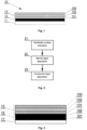
- Fig. 1 schematically illustrates the optoelectronic foil in a cross-section, showing the layered foil construction.
- the optoelectronic foil has a substrate 11 with a barrier layer 12 on which a conductive layer 13 comprising at least one oxide layer 131 and at least one metal layer 132 is deposited.
- the substrate 11 of the optoelectronic foil 10 may be made of a variety of transparent substrate materials selected from the group consisting of plastics and/or plastics with nanocomposites of inorganic materials.
- plastics for the substrate 11 may be provided in the form of at least one type of material selected from the group consisting of polyethylene terephthalate (PET), polyethylene naphthalene (PEN), polyethylene (PE), polypropylene (PP), polyethersulfone (PES), polyimide (PI), polystyrene (PS), ethylene/tetrafluoroethylene (ETFE) and polymers evaporated onto the surface from the group of poly-p-xylenes collectively referred to as parylene.
- PET polyethylene terephthalate
- PEN polyethylene naphthalene
- PE polyethylene
- PP polypropylene
- PES polyethersulfone
- PI polyimide
- PS polystyrene
- EFE ethylene/tetrafluoro
- the barrier layer 12 of the foil 10 has a barrier function and prevents against moisture and oxygen penetration from the substrate 11 into the conductive layer 13, thus ensuring a significant reduction of degradation processes of the conductive layer that constitutes the optoelectronic element of the foil 10 and of the active layers of the device that can be deposited onto the optoelectronic foil 10.
- the barrier layer 12 consists of at least one material selected from the group consisting of silicon oxides (SiO x ), aluminium oxides (Al 2 O 3 , AlO x N y ), titanium oxides (TiO x ), silicon oxynitrides SiON, silicon nitrides (Si 3 N 4 , SiN x ), organic silicon compounds (SiC x H y ), zirconium oxide (ZrO 2 ), hafnium oxide (HfO 2 ), chromium oxides (CrO, Cr 2 O 3 , CrO 2 , CrO 3 , CrO 5 ) and parylene.
- the barrier layer may consist of at least two different materials selected from the group consisting of silicon oxides (SiO x ), aluminium oxides (Al 2 O 3 , AlO x N y ), titanium oxides (TiO x ), silicon oxynitride SiON, silicon nitrides (Si 3 N 4 , SiN x ), organic silicon compounds (SiC x H y ), zirconium oxide (ZrO 2 ), hafnium oxide (HfO 2 ), chromium oxides (CrO, Cr 2 O 3 , CrO 2 , CrO 3 , CrO 5 ) and parylene.
- silicon oxides SiO x
- aluminium oxides Al 2 O 3 , AlO x N y
- titanium oxides TiO x
- silicon oxynitride SiON silicon nitrides
- Si 3 N 4 silicon nitrides
- SiN x organic silicon compounds
- ZrO 2 zirconium oxide
- the barrier layer may take, for example, the form of a monolayer consisting of only one material, such as Al 2 O 3 .
- the barrier layer may take the form of a monolayer comprising at least two different materials and may be made, for example, of Al 2 O 3 doped with TiO 2 .
- the barrier layer 12 may consist of at least two different materials, and it may take the form of a multi-layer comprising, within the barrier layer 12, at least two sub-layers stacked one on the other, wherein each sub-layer may be made of different material or materials.
- the barrier layer may have two sublayers, where one sublayer is made of Al 2 O 3 , and the other sublayer is made of TiO 2 .
- Each sublayer within the barrier layer 12 may be of the same or different thickness, preferably in the range between 5 and 500 nm, regardless of the thickness of another sublayer.
- the barrier layer 12 may comprise two sublayers, each made of a different material, selected from the group of materials listed above.
- the barrier layer 12 may have a total thickness preferably in the range between 5 and 1000 nm.
- the conductive layer 13 is an optoelectronic active layer of the foil with conductive properties.
- the conductive layer 13 comprises at least one oxide layer 131, 133 and at least one metal layer 132 stacked one on the other.
- the conductive layer comprises at least two oxide layers 131 and 133, or more than two oxide layers, separated by metal layers 132 to form a sandwich architecture. All layers 131, 132, 133 are stacked in the conductive layer 13 one on the other, substantially in parallel.
- the oxide layer 131, 133 is made of at least one oxide selected from the group consisting of: ZnO, AZO (aluminium zinc oxide), SnO 2 , IZO (indium zinc oxide), FTO (fluorine tin oxide), ZTO (tin zinc oxide), ITO (tin indium oxide), GZO (zinc gallium oxide), GIO (indium gallium oxide), In 2 O 3 , Sb:SnO 2 , IO:H (hydrogen indium oxide), CdO, Zn 2 SnO 4 , ZnSnO 3 , Zn 2 In 2 O 5 , NiO x , NiO x :Li, TiO x , ZnS, ZnSe, Te 2 O 3 , MoO x , V 2 O 5 and WO 3 .
- the oxide layer 13 of the optoelectronic foil 10 the oxide selected from the group consisting of: ZnO, AZO (aluminium zinc oxide), SnO 2
- the oxide layer 131, 133 may take the form of a monolayer and consist of one type of oxide, from the group of oxides listed above, for example ZnO.
- the oxide layer may take the form of a monolayer and consist of more than one material, for example the oxide layer 131, 133, in the form of a monolayer may be made of ZnO doped with Al.
- the oxide layer 131, 133 may consist of at least two different oxides and may take the form of a multilayer comprising, within one oxide layer 131, 133, at least two sublayers, wherein each sublayer is made of a different oxide material comprising at least one oxide.
- the oxide layer 131, 133 may consist of two sublayers stacked one on the other within one oxide layer 131, 133, wherein one sublayer is made of ZnO and the other sublayer is made of AZO or IZTO doped with Al.
- the optoelectronic foil may comprise at least two oxide layers 131, 133, wherein one oxide layer takes the form of a monolayer and another oxide layer takes the form of a multilayer comprising at least two sublayers made of different oxide materials.
- the metal layer 132 is made of at least one metal selected from the group consisting of: Al, Ti, Ni, Cr, Au, Mg, Ta, Ge, Ag, Cu, Zr, Pt and W.
- the metal layer 132 may preferably have a thickness in the range between 2 and 20 nm.
- the conductive layer 13 may comprise, as schematically shown in Fig. 1 , two oxide layers 131, 133, each of which may be a multi- or monolayer, and one metal layer 132 separating the two oxide layers.
- the conductive layer 13 may have three oxide layers and two metal layers stacked within the conductive layer one alternately on the other, so that each of the metal layers separates the two adjacent oxide layers.
- the conductive layer may have n oxide layers 131, 133, each of which may be a multi- or monolayer, and n-1 metal layers stacked one on the other, so that each metal layer 132 separates two adjacent oxide layers 132, 133 forming a sandwich structure, where n is any number selected from the set of natural numbers.
- n may be 2, 3, 4, 5, 6 or 7.
- n may be up to 33, or n may be more than 33.
- Fig. 2 schematically shows a manufacturing method of the optoelectronic foil.
- a substrate material 11 is prepared in order to produce the optoelectronic foil in step 21.
- the preparation process involves thorough cleaning and activation of the selected substrate surface.
- the cleaning and activation process of step 21 is implemented using at least one technique selected from the group consisting of plasma treatment, corona discharge treatment, carbon dioxide treatment, cleaning with solvents such as acetone, isopropanol, water, or mixtures of acetone and water or a mixture of isopropanol and water, as well as surface treatment with ultraviolet (UV) radiation and ozone.
- a barrier layer 12 is deposited onto the cleaned and activated surface of the substrate 11.
- step 22 may include one or more steps.
- the barrier layer may be deposited in one step.
- the deposition step 22 may comprise several sub-steps, each involving depositing one sublayer onto the barrier layer 12.
- the deposition in step 22 is implemented so that a sublayer of one material is deposited in the first step, and then a sublayer of another material selected from the material group for the barrier layer 12 listed above is deposited.
- the processes of depositing the barrier layer 12 having both the structure of a multilayer and monolayer may be implemented using at least one known deposition technique selected from the group consisting of: atomic layer deposition (ALD) technique, magnetron sputtering technique, electron-beam sputtering technique and thermal evaporation technique.
- ALD atomic layer deposition
- a conductive layer 13 is deposited onto the barrier layer having a multi- or monolayer structure, wherein each of the sublayers of the conductive layer 13, that is at least two oxide layers 131, 132 and at least one metal layer 132, is deposited onto the barrier layer 12 individually, in order to obtain the appropriate functionality and architecture of the conductive layer 13, e.g. a sandwich architecture.
- Each of the sublayers 131, 132, 133 of the conductive layer can be deposited using various deposition methods also known from the art, selected from the group consisting of: atomic layer deposition (ALD) technique, magnetron sputtering, electron-beam sputtering technique and thermal evaporation technique.
- ALD atomic layer deposition
- Each of the sub-layers 131, 132, 133 may be deposited using the same or different deposition techniques.
- the oxide layer 131, 133 may be deposited in step 23 in single step or several steps, each of which may be implemented using one technique as well as different deposition techniques.
- the oxide layer 131, 133 may be deposited in single step 23.
- the oxide layer may be deposited in several steps in step 23, each step including depositing one sublayer within the oxide layer 131, 133.
- the optoelectronic foil obtained combines barrier properties and an efficient conductive layer 13, which preferably may have the architecture of an electrode, depending on the materials used as the materials for oxide and metal layers 131, 132, 133, respectively.
- the conductive layer 13 is integrated with an flexible substrate 11, 12 having barrier properties.
- the barrier layer of the optoelectronic foil has water vapor permeability rates (WVTR) ranging between 10 -3 and 10 -6 g/m 2 per day and has stable barrier properties, including high hydrophobicity and UV radiation resistance, which improves the lifespan of the conductive layer of the foil according to the present invention.
- WVTR water vapor permeability rates
- the optoelectronic foil is flexible and is characterised by relatively high transparency, while the conductive layer of the foil has good conductivity and is an alternative to the single, thicker conductive ITO (indium tin oxide) layer known in the prior art that is relatively brittle, has limited conductivity and is expensive.
- ITO indium tin oxide
- the optoelectronic foil according to one embodiment of the present invention is schematically shown as a cross-section in Fig. 1 .
- the optoelectronic foil comprises a substrate 11, which in this embodiment is made of a plastic, namely polyethylene terephthalate (PET).
- PET polyethylene terephthalate
- the top surface of substrate 11 was cleaned and activated using oxygen plasma treatment.
- a single barrier layer 12 made of AlO x with a thickness of 300 nm, which is an amorphous layer was deposited onto the top surface of substrate 11 thus prepared in the reactive magnetron sputtering process.
- a conductive layer 13 was deposited onto the barrier layer 12 in the reactive magnetron sputtering process, comprising the first oxide layer 131 made of ITO with a thickness of 20 nm, a metal layer 132 made of Ag with a thickness of 9 nm and a second oxide layer 133 made of ITO with a thickness of 20 nm.
- the tests conducted yielded a surface resistance of the conductive layer 13 of 12 ⁇ / ⁇ , a WVTR permeability rate of 10 -3 g/m 2 per day and light transmission in the visible spectrum in the range of 70-78%.
- the optoelectronic foil according to another embodiment of the present invention is schematically shown as a cross-section in Fig. 3 .
- the optoelectronic foil comprises a substrate 11, which in this embodiment is made of a plastic, namely polyethylene terephthalate (PET).
- PET polyethylene terephthalate
- the top surface of substrate 11 was cleaned and activated using oxygen plasma treatment.
- a barrier layer 12 in the form of an AlO x layer 121 with a thickness of 100 nm and a TiO x layer 122 with a thickness of 150 nm, which constitute amorphous layers, were deposited onto the top surface of substrate 11 thus prepared in the reactive magnetron sputtering process.
- a conductive layer 13 was deposited onto the barrier layer 12 in the reactive magnetron sputtering process, containing the first oxide layer 131 made of ITO with a thickness of 20 nm, a metal layer 132 made of Ag with a thickness of 9 nm and a second oxide layer 133 made of ITO with a thickness of 20 nm.
- the tests conducted yielded a surface resistance of the conductive layer 13 of 12 ⁇ / ⁇ , a WVTR permeability rate of less than 5*10 -4 g/m 2 per day and light transmission in the visible spectrum in the range of 67-80%.
Landscapes
- Chemical & Material Sciences (AREA)
- Chemical Kinetics & Catalysis (AREA)
- Engineering & Computer Science (AREA)
- Materials Engineering (AREA)
- Mechanical Engineering (AREA)
- Metallurgy (AREA)
- Organic Chemistry (AREA)
- Physics & Mathematics (AREA)
- Nonlinear Science (AREA)
- General Physics & Mathematics (AREA)
- Crystallography & Structural Chemistry (AREA)
- Mathematical Physics (AREA)
- Optics & Photonics (AREA)
- Electromagnetism (AREA)
- Laminated Bodies (AREA)
- Electroluminescent Light Sources (AREA)
Applications Claiming Priority (2)
| Application Number | Priority Date | Filing Date | Title |
|---|---|---|---|
| PL420300A PL233211B1 (pl) | 2017-01-25 | 2017-01-25 | Folia optoelektroniczna oraz sposób wytwarzania folii optoelektronicznej |
| PCT/PL2018/000008 WO2018139945A1 (en) | 2017-01-25 | 2018-01-24 | Optoelectronic foil and manufacturing method of optoelectronic foil |
Publications (2)
| Publication Number | Publication Date |
|---|---|
| EP3574528A1 EP3574528A1 (en) | 2019-12-04 |
| EP3574528B1 true EP3574528B1 (en) | 2024-03-13 |
Family
ID=61683865
Family Applications (1)
| Application Number | Title | Priority Date | Filing Date |
|---|---|---|---|
| EP18711714.8A Active EP3574528B1 (en) | 2017-01-25 | 2018-01-24 | Optoelectronic foil and manufacturing method of optoelectronic foil |
Country Status (8)
| Country | Link |
|---|---|
| US (1) | US20190348621A1 (enExample) |
| EP (1) | EP3574528B1 (enExample) |
| JP (1) | JP7206559B2 (enExample) |
| CN (1) | CN110291647B (enExample) |
| ES (1) | ES2975275T3 (enExample) |
| FI (1) | FI3574528T3 (enExample) |
| PL (1) | PL233211B1 (enExample) |
| WO (1) | WO2018139945A1 (enExample) |
Families Citing this family (8)
| Publication number | Priority date | Publication date | Assignee | Title |
|---|---|---|---|---|
| PL425218A1 (pl) * | 2018-04-13 | 2019-10-21 | Centrum Badań I Rozwoju Technologii Dla Przemysłu Spółka Akcyjna | Krzemowe ogniwo fotowoltaiczne i sposób wytwarzania krzemowych ogniw fotowoltaicznych |
| CN109979977A (zh) | 2019-03-28 | 2019-07-05 | 武汉华星光电半导体显示技术有限公司 | Oled显示面板及其制备方法 |
| WO2021157373A1 (ja) * | 2020-02-04 | 2021-08-12 | 三井金属鉱業株式会社 | キャリア付金属箔 |
| CN111638610A (zh) * | 2020-07-20 | 2020-09-08 | 宁波材料所杭州湾研究院 | 一种兼具可见光高透过和隔热的柔性智能调光膜及其制备方法 |
| EP4209341A4 (en) * | 2020-09-04 | 2024-10-23 | Dexerials Corporation | CONDUCTIVE LAMINATED PRODUCT, OPTICAL DEVICE USING SAME, AND MANUFACTURING METHOD FOR CONDUCTIVE LAMINATED PRODUCT |
| JP7230131B2 (ja) * | 2020-09-04 | 2023-02-28 | デクセリアルズ株式会社 | 導電性積層体及びこれを用いた光学装置、導電性積層体の製造方法 |
| ES2980711T3 (es) | 2021-03-23 | 2024-10-02 | Saule S A | Una estructura multicapa transmisora de luz para dispositivos optoelectrónicos |
| US11545453B2 (en) * | 2021-04-19 | 2023-01-03 | Nanya Technology Corporation | Semiconductor device with barrier layer and method for fabricating the same |
Citations (1)
| Publication number | Priority date | Publication date | Assignee | Title |
|---|---|---|---|---|
| WO2012029780A1 (ja) * | 2010-09-03 | 2012-03-08 | 大日本印刷株式会社 | 太陽電池および太陽電池モジュール |
Family Cites Families (19)
| Publication number | Priority date | Publication date | Assignee | Title |
|---|---|---|---|---|
| US5667853A (en) * | 1995-03-22 | 1997-09-16 | Toppan Printing Co., Ltd. | Multilayered conductive film, and transparent electrode substrate and liquid crystal device using the same |
| JPH1024520A (ja) * | 1996-07-11 | 1998-01-27 | Mitsui Petrochem Ind Ltd | 透明導電性積層体 |
| US6379509B2 (en) * | 1998-01-20 | 2002-04-30 | 3M Innovative Properties Company | Process for forming electrodes |
| EP1921491A1 (en) * | 1998-11-30 | 2008-05-14 | Teijin Limited | Liquid crystal device and transparent conductive substrate suitable for the same |
| JP3862466B2 (ja) * | 2000-02-29 | 2006-12-27 | 三井化学株式会社 | 透明電極 |
| US20040229051A1 (en) * | 2003-05-15 | 2004-11-18 | General Electric Company | Multilayer coating package on flexible substrates for electro-optical devices |
| JP4742584B2 (ja) * | 2004-03-23 | 2011-08-10 | 株式会社豊田中央研究所 | 電極 |
| CN102714228A (zh) * | 2010-01-18 | 2012-10-03 | 应用材料公司 | 制造具有高转换效率的薄膜太阳能电池 |
| FR2973946B1 (fr) * | 2011-04-08 | 2013-03-22 | Saint Gobain | Dispositif électronique a couches |
| EP2720276A4 (en) * | 2011-06-10 | 2014-12-24 | Posco | SOLAR CELL SUBSTRATE, MANUFACTURING METHOD AND SOLAR CELL THEREFOR |
| US9018715B2 (en) * | 2012-11-30 | 2015-04-28 | Silicon Laboratories Inc. | Gas-diffusion barriers for MEMS encapsulation |
| TWI495404B (zh) * | 2013-06-21 | 2015-08-01 | Chi Mei Corp | 軟性基板用組成物及軟性基板 |
| EP3016162B1 (en) * | 2013-09-30 | 2020-07-22 | LG Chem, Ltd. | Substrate for organic electronic devices and production method therefor |
| EP2871681A1 (en) * | 2013-11-07 | 2015-05-13 | Saint-Gobain Glass France | Back contact substrate for a photovoltaic cell or module |
| JP2016103443A (ja) * | 2014-11-28 | 2016-06-02 | パイオニア株式会社 | 発光装置 |
| JP5994884B2 (ja) * | 2015-03-03 | 2016-09-21 | コニカミノルタ株式会社 | 有機エレクトロルミネッセンス素子および照明装置 |
| CN106158901B (zh) * | 2015-03-24 | 2020-06-23 | 上海和辉光电有限公司 | 一种混合型薄膜及其制备方法、以及柔性oled显示器 |
| US10573856B2 (en) * | 2015-05-14 | 2020-02-25 | GM Global Technology Operations LLC | Barrier layer coatings for battery pouch cell seal |
| WO2016190283A1 (ja) * | 2015-05-26 | 2016-12-01 | 東レ株式会社 | ピロメテンホウ素錯体、色変換組成物、色変換フィルムならびにそれを含む光源ユニット、ディスプレイおよび照明 |
-
2017
- 2017-01-25 PL PL420300A patent/PL233211B1/pl unknown
-
2018
- 2018-01-24 CN CN201880008575.4A patent/CN110291647B/zh active Active
- 2018-01-24 ES ES18711714T patent/ES2975275T3/es active Active
- 2018-01-24 JP JP2019539927A patent/JP7206559B2/ja active Active
- 2018-01-24 EP EP18711714.8A patent/EP3574528B1/en active Active
- 2018-01-24 FI FIEP18711714.8T patent/FI3574528T3/fi active
- 2018-01-24 WO PCT/PL2018/000008 patent/WO2018139945A1/en not_active Ceased
-
2019
- 2019-07-25 US US16/521,645 patent/US20190348621A1/en active Pending
Patent Citations (1)
| Publication number | Priority date | Publication date | Assignee | Title |
|---|---|---|---|---|
| WO2012029780A1 (ja) * | 2010-09-03 | 2012-03-08 | 大日本印刷株式会社 | 太陽電池および太陽電池モジュール |
Also Published As
| Publication number | Publication date |
|---|---|
| EP3574528A1 (en) | 2019-12-04 |
| PL233211B1 (pl) | 2019-09-30 |
| ES2975275T3 (es) | 2024-07-04 |
| US20190348621A1 (en) | 2019-11-14 |
| PL420300A1 (pl) | 2018-07-30 |
| JP2020505736A (ja) | 2020-02-20 |
| CN110291647B (zh) | 2024-03-26 |
| JP7206559B2 (ja) | 2023-01-18 |
| FI3574528T3 (fi) | 2024-04-23 |
| WO2018139945A1 (en) | 2018-08-02 |
| CN110291647A (zh) | 2019-09-27 |
Similar Documents
| Publication | Publication Date | Title |
|---|---|---|
| EP3574528B1 (en) | Optoelectronic foil and manufacturing method of optoelectronic foil | |
| US9059425B2 (en) | Multilayer electronic device having one or more barrier stacks | |
| US8766280B2 (en) | Protective substrate for a device that collects or emits radiation | |
| EP3001428B1 (en) | Conductive film and electronic device having conductive film | |
| CN113299426B (zh) | 一种透明导电阻隔薄膜、其制备方法及应用 | |
| JP2020505736A5 (enExample) | ||
| KR101809296B1 (ko) | 투명전극 및 이를 포함하는 전자 소자 | |
| US9704610B2 (en) | Manganese tin oxide based transparent conducting oxide and transparent conductive film and method for fabricating transparent conductive film using the same | |
| CN106887274A (zh) | 一种柔性透明导电薄膜及其制备方法 | |
| KR20140090876A (ko) | 다층 구조의 투명 전극 | |
| KR101816972B1 (ko) | TiO2/Ag/TiO2 다층박막 구조를 갖는 플렉시블 투명 전극 및 그 제조방법 | |
| KR20160020834A (ko) | 배리어 필름 구조체 및 이를 구비하는 유기전자소자 | |
| EP4064378B1 (en) | A light-transmissive multilayer structure for optoelectronic devices | |
| CN113614926A (zh) | 透明的多层组件和制造方法 |
Legal Events
| Date | Code | Title | Description |
|---|---|---|---|
| STAA | Information on the status of an ep patent application or granted ep patent |
Free format text: STATUS: UNKNOWN |
|
| STAA | Information on the status of an ep patent application or granted ep patent |
Free format text: STATUS: THE INTERNATIONAL PUBLICATION HAS BEEN MADE |
|
| PUAI | Public reference made under article 153(3) epc to a published international application that has entered the european phase |
Free format text: ORIGINAL CODE: 0009012 |
|
| STAA | Information on the status of an ep patent application or granted ep patent |
Free format text: STATUS: REQUEST FOR EXAMINATION WAS MADE |
|
| 17P | Request for examination filed |
Effective date: 20190823 |
|
| AK | Designated contracting states |
Kind code of ref document: A1 Designated state(s): AL AT BE BG CH CY CZ DE DK EE ES FI FR GB GR HR HU IE IS IT LI LT LU LV MC MK MT NL NO PL PT RO RS SE SI SK SM TR |
|
| AX | Request for extension of the european patent |
Extension state: BA ME |
|
| RAP1 | Party data changed (applicant data changed or rights of an application transferred) |
Owner name: SAULE SPOLKA AKCYJNA |
|
| DAV | Request for validation of the european patent (deleted) | ||
| DAX | Request for extension of the european patent (deleted) | ||
| STAA | Information on the status of an ep patent application or granted ep patent |
Free format text: STATUS: EXAMINATION IS IN PROGRESS |
|
| 17Q | First examination report despatched |
Effective date: 20200528 |
|
| GRAP | Despatch of communication of intention to grant a patent |
Free format text: ORIGINAL CODE: EPIDOSNIGR1 |
|
| STAA | Information on the status of an ep patent application or granted ep patent |
Free format text: STATUS: GRANT OF PATENT IS INTENDED |
|
| RIC1 | Information provided on ipc code assigned before grant |
Ipc: H10K 50/816 20230101ALI20231012BHEP Ipc: H10K 30/82 20230101ALI20231012BHEP Ipc: H10K 102/10 20230101ALI20231012BHEP Ipc: H01L 31/0392 20060101ALI20231012BHEP Ipc: H01L 31/0224 20060101AFI20231012BHEP |
|
| INTG | Intention to grant announced |
Effective date: 20231031 |
|
| GRAS | Grant fee paid |
Free format text: ORIGINAL CODE: EPIDOSNIGR3 |
|
| GRAA | (expected) grant |
Free format text: ORIGINAL CODE: 0009210 |
|
| STAA | Information on the status of an ep patent application or granted ep patent |
Free format text: STATUS: THE PATENT HAS BEEN GRANTED |
|
| RAP3 | Party data changed (applicant data changed or rights of an application transferred) |
Owner name: SAULE SPOLKA AKCYJNA |
|
| AK | Designated contracting states |
Kind code of ref document: B1 Designated state(s): AL AT BE BG CH CY CZ DE DK EE ES FI FR GB GR HR HU IE IS IT LI LT LU LV MC MK MT NL NO PL PT RO RS SE SI SK SM TR |
|
| REG | Reference to a national code |
Ref country code: GB Ref legal event code: FG4D |
|
| REG | Reference to a national code |
Ref country code: CH Ref legal event code: EP |
|
| REG | Reference to a national code |
Ref country code: DE Ref legal event code: R096 Ref document number: 602018066536 Country of ref document: DE |
|
| P01 | Opt-out of the competence of the unified patent court (upc) registered |
Effective date: 20240301 |
|
| REG | Reference to a national code |
Ref country code: IE Ref legal event code: FG4D |
|
| REG | Reference to a national code |
Ref country code: SE Ref legal event code: TRGR |
|
| REG | Reference to a national code |
Ref country code: FI Ref legal event code: FGE |
|
| REG | Reference to a national code |
Ref country code: NL Ref legal event code: FP |
|
| REG | Reference to a national code |
Ref country code: ES Ref legal event code: FG2A Ref document number: 2975275 Country of ref document: ES Kind code of ref document: T3 Effective date: 20240704 |
|
| PG25 | Lapsed in a contracting state [announced via postgrant information from national office to epo] |
Ref country code: LT Free format text: LAPSE BECAUSE OF FAILURE TO SUBMIT A TRANSLATION OF THE DESCRIPTION OR TO PAY THE FEE WITHIN THE PRESCRIBED TIME-LIMIT Effective date: 20240313 |
|
| REG | Reference to a national code |
Ref country code: LT Ref legal event code: MG9D |
|
| PG25 | Lapsed in a contracting state [announced via postgrant information from national office to epo] |
Ref country code: GR Free format text: LAPSE BECAUSE OF FAILURE TO SUBMIT A TRANSLATION OF THE DESCRIPTION OR TO PAY THE FEE WITHIN THE PRESCRIBED TIME-LIMIT Effective date: 20240614 |
|
| PG25 | Lapsed in a contracting state [announced via postgrant information from national office to epo] |
Ref country code: RS Free format text: LAPSE BECAUSE OF FAILURE TO SUBMIT A TRANSLATION OF THE DESCRIPTION OR TO PAY THE FEE WITHIN THE PRESCRIBED TIME-LIMIT Effective date: 20240613 Ref country code: HR Free format text: LAPSE BECAUSE OF FAILURE TO SUBMIT A TRANSLATION OF THE DESCRIPTION OR TO PAY THE FEE WITHIN THE PRESCRIBED TIME-LIMIT Effective date: 20240313 |
|
| PG25 | Lapsed in a contracting state [announced via postgrant information from national office to epo] |
Ref country code: RS Free format text: LAPSE BECAUSE OF FAILURE TO SUBMIT A TRANSLATION OF THE DESCRIPTION OR TO PAY THE FEE WITHIN THE PRESCRIBED TIME-LIMIT Effective date: 20240613 Ref country code: NO Free format text: LAPSE BECAUSE OF FAILURE TO SUBMIT A TRANSLATION OF THE DESCRIPTION OR TO PAY THE FEE WITHIN THE PRESCRIBED TIME-LIMIT Effective date: 20240613 Ref country code: LT Free format text: LAPSE BECAUSE OF FAILURE TO SUBMIT A TRANSLATION OF THE DESCRIPTION OR TO PAY THE FEE WITHIN THE PRESCRIBED TIME-LIMIT Effective date: 20240313 Ref country code: HR Free format text: LAPSE BECAUSE OF FAILURE TO SUBMIT A TRANSLATION OF THE DESCRIPTION OR TO PAY THE FEE WITHIN THE PRESCRIBED TIME-LIMIT Effective date: 20240313 Ref country code: GR Free format text: LAPSE BECAUSE OF FAILURE TO SUBMIT A TRANSLATION OF THE DESCRIPTION OR TO PAY THE FEE WITHIN THE PRESCRIBED TIME-LIMIT Effective date: 20240614 Ref country code: BG Free format text: LAPSE BECAUSE OF FAILURE TO SUBMIT A TRANSLATION OF THE DESCRIPTION OR TO PAY THE FEE WITHIN THE PRESCRIBED TIME-LIMIT Effective date: 20240313 |
|
| REG | Reference to a national code |
Ref country code: AT Ref legal event code: MK05 Ref document number: 1666590 Country of ref document: AT Kind code of ref document: T Effective date: 20240313 |
|
| PG25 | Lapsed in a contracting state [announced via postgrant information from national office to epo] |
Ref country code: LV Free format text: LAPSE BECAUSE OF FAILURE TO SUBMIT A TRANSLATION OF THE DESCRIPTION OR TO PAY THE FEE WITHIN THE PRESCRIBED TIME-LIMIT Effective date: 20240313 |
|
| PG25 | Lapsed in a contracting state [announced via postgrant information from national office to epo] |
Ref country code: IS Free format text: LAPSE BECAUSE OF FAILURE TO SUBMIT A TRANSLATION OF THE DESCRIPTION OR TO PAY THE FEE WITHIN THE PRESCRIBED TIME-LIMIT Effective date: 20240713 |
|
| PG25 | Lapsed in a contracting state [announced via postgrant information from national office to epo] |
Ref country code: PT Free format text: LAPSE BECAUSE OF FAILURE TO SUBMIT A TRANSLATION OF THE DESCRIPTION OR TO PAY THE FEE WITHIN THE PRESCRIBED TIME-LIMIT Effective date: 20240715 Ref country code: SM Free format text: LAPSE BECAUSE OF FAILURE TO SUBMIT A TRANSLATION OF THE DESCRIPTION OR TO PAY THE FEE WITHIN THE PRESCRIBED TIME-LIMIT Effective date: 20240313 |
|
| PG25 | Lapsed in a contracting state [announced via postgrant information from national office to epo] |
Ref country code: EE Free format text: LAPSE BECAUSE OF FAILURE TO SUBMIT A TRANSLATION OF THE DESCRIPTION OR TO PAY THE FEE WITHIN THE PRESCRIBED TIME-LIMIT Effective date: 20240313 Ref country code: CZ Free format text: LAPSE BECAUSE OF FAILURE TO SUBMIT A TRANSLATION OF THE DESCRIPTION OR TO PAY THE FEE WITHIN THE PRESCRIBED TIME-LIMIT Effective date: 20240313 |
|
| PG25 | Lapsed in a contracting state [announced via postgrant information from national office to epo] |
Ref country code: AT Free format text: LAPSE BECAUSE OF FAILURE TO SUBMIT A TRANSLATION OF THE DESCRIPTION OR TO PAY THE FEE WITHIN THE PRESCRIBED TIME-LIMIT Effective date: 20240313 |
|
| PG25 | Lapsed in a contracting state [announced via postgrant information from national office to epo] |
Ref country code: PL Free format text: LAPSE BECAUSE OF FAILURE TO SUBMIT A TRANSLATION OF THE DESCRIPTION OR TO PAY THE FEE WITHIN THE PRESCRIBED TIME-LIMIT Effective date: 20240313 |
|
| PG25 | Lapsed in a contracting state [announced via postgrant information from national office to epo] |
Ref country code: SK Free format text: LAPSE BECAUSE OF FAILURE TO SUBMIT A TRANSLATION OF THE DESCRIPTION OR TO PAY THE FEE WITHIN THE PRESCRIBED TIME-LIMIT Effective date: 20240313 |
|
| PG25 | Lapsed in a contracting state [announced via postgrant information from national office to epo] |
Ref country code: SM Free format text: LAPSE BECAUSE OF FAILURE TO SUBMIT A TRANSLATION OF THE DESCRIPTION OR TO PAY THE FEE WITHIN THE PRESCRIBED TIME-LIMIT Effective date: 20240313 Ref country code: SK Free format text: LAPSE BECAUSE OF FAILURE TO SUBMIT A TRANSLATION OF THE DESCRIPTION OR TO PAY THE FEE WITHIN THE PRESCRIBED TIME-LIMIT Effective date: 20240313 Ref country code: RO Free format text: LAPSE BECAUSE OF FAILURE TO SUBMIT A TRANSLATION OF THE DESCRIPTION OR TO PAY THE FEE WITHIN THE PRESCRIBED TIME-LIMIT Effective date: 20240313 Ref country code: PT Free format text: LAPSE BECAUSE OF FAILURE TO SUBMIT A TRANSLATION OF THE DESCRIPTION OR TO PAY THE FEE WITHIN THE PRESCRIBED TIME-LIMIT Effective date: 20240715 Ref country code: PL Free format text: LAPSE BECAUSE OF FAILURE TO SUBMIT A TRANSLATION OF THE DESCRIPTION OR TO PAY THE FEE WITHIN THE PRESCRIBED TIME-LIMIT Effective date: 20240313 Ref country code: IS Free format text: LAPSE BECAUSE OF FAILURE TO SUBMIT A TRANSLATION OF THE DESCRIPTION OR TO PAY THE FEE WITHIN THE PRESCRIBED TIME-LIMIT Effective date: 20240713 Ref country code: EE Free format text: LAPSE BECAUSE OF FAILURE TO SUBMIT A TRANSLATION OF THE DESCRIPTION OR TO PAY THE FEE WITHIN THE PRESCRIBED TIME-LIMIT Effective date: 20240313 Ref country code: CZ Free format text: LAPSE BECAUSE OF FAILURE TO SUBMIT A TRANSLATION OF THE DESCRIPTION OR TO PAY THE FEE WITHIN THE PRESCRIBED TIME-LIMIT Effective date: 20240313 Ref country code: AT Free format text: LAPSE BECAUSE OF FAILURE TO SUBMIT A TRANSLATION OF THE DESCRIPTION OR TO PAY THE FEE WITHIN THE PRESCRIBED TIME-LIMIT Effective date: 20240313 |
|
| REG | Reference to a national code |
Ref country code: DE Ref legal event code: R079 Ref document number: 602018066536 Country of ref document: DE Free format text: PREVIOUS MAIN CLASS: H01L0031022400 Ipc: H10F0077200000 |
|
| REG | Reference to a national code |
Ref country code: DE Ref legal event code: R097 Ref document number: 602018066536 Country of ref document: DE |
|
| PG25 | Lapsed in a contracting state [announced via postgrant information from national office to epo] |
Ref country code: DK Free format text: LAPSE BECAUSE OF FAILURE TO SUBMIT A TRANSLATION OF THE DESCRIPTION OR TO PAY THE FEE WITHIN THE PRESCRIBED TIME-LIMIT Effective date: 20240313 |
|
| PLBE | No opposition filed within time limit |
Free format text: ORIGINAL CODE: 0009261 |
|
| STAA | Information on the status of an ep patent application or granted ep patent |
Free format text: STATUS: NO OPPOSITION FILED WITHIN TIME LIMIT |
|
| PG25 | Lapsed in a contracting state [announced via postgrant information from national office to epo] |
Ref country code: DK Free format text: LAPSE BECAUSE OF FAILURE TO SUBMIT A TRANSLATION OF THE DESCRIPTION OR TO PAY THE FEE WITHIN THE PRESCRIBED TIME-LIMIT Effective date: 20240313 |
|
| PGFP | Annual fee paid to national office [announced via postgrant information from national office to epo] |
Ref country code: NL Payment date: 20250127 Year of fee payment: 8 |
|
| 26N | No opposition filed |
Effective date: 20241216 |
|
| PGFP | Annual fee paid to national office [announced via postgrant information from national office to epo] |
Ref country code: DE Payment date: 20250127 Year of fee payment: 8 |
|
| PGFP | Annual fee paid to national office [announced via postgrant information from national office to epo] |
Ref country code: FI Payment date: 20250127 Year of fee payment: 8 |
|
| PGFP | Annual fee paid to national office [announced via postgrant information from national office to epo] |
Ref country code: ES Payment date: 20250211 Year of fee payment: 8 |
|
| PGFP | Annual fee paid to national office [announced via postgrant information from national office to epo] |
Ref country code: SE Payment date: 20250127 Year of fee payment: 8 |
|
| PG25 | Lapsed in a contracting state [announced via postgrant information from national office to epo] |
Ref country code: SI Free format text: LAPSE BECAUSE OF FAILURE TO SUBMIT A TRANSLATION OF THE DESCRIPTION OR TO PAY THE FEE WITHIN THE PRESCRIBED TIME-LIMIT Effective date: 20240313 |
|
| PGFP | Annual fee paid to national office [announced via postgrant information from national office to epo] |
Ref country code: CH Payment date: 20250201 Year of fee payment: 8 |
|
| PGFP | Annual fee paid to national office [announced via postgrant information from national office to epo] |
Ref country code: FR Payment date: 20250127 Year of fee payment: 8 |
|
| PGFP | Annual fee paid to national office [announced via postgrant information from national office to epo] |
Ref country code: IT Payment date: 20250127 Year of fee payment: 8 Ref country code: GB Payment date: 20250127 Year of fee payment: 8 |
|
| PG25 | Lapsed in a contracting state [announced via postgrant information from national office to epo] |
Ref country code: LU Free format text: LAPSE BECAUSE OF NON-PAYMENT OF DUE FEES Effective date: 20250124 Ref country code: MC Free format text: LAPSE BECAUSE OF FAILURE TO SUBMIT A TRANSLATION OF THE DESCRIPTION OR TO PAY THE FEE WITHIN THE PRESCRIBED TIME-LIMIT Effective date: 20240313 |
|
| PG25 | Lapsed in a contracting state [announced via postgrant information from national office to epo] |
Ref country code: BE Free format text: LAPSE BECAUSE OF NON-PAYMENT OF DUE FEES Effective date: 20250131 |
|
| REG | Reference to a national code |
Ref country code: BE Ref legal event code: MM Effective date: 20250131 |