EP3574528B1 - Optoelectronic foil and manufacturing method of optoelectronic foil - Google Patents
Optoelectronic foil and manufacturing method of optoelectronic foil Download PDFInfo
- Publication number
- EP3574528B1 EP3574528B1 EP18711714.8A EP18711714A EP3574528B1 EP 3574528 B1 EP3574528 B1 EP 3574528B1 EP 18711714 A EP18711714 A EP 18711714A EP 3574528 B1 EP3574528 B1 EP 3574528B1
- Authority
- EP
- European Patent Office
- Prior art keywords
- oxide
- layer
- optoelectronic
- barrier layer
- foil
- Prior art date
- Legal status (The legal status is an assumption and is not a legal conclusion. Google has not performed a legal analysis and makes no representation as to the accuracy of the status listed.)
- Active
Links
- 239000011888 foil Substances 0.000 title claims description 63
- 230000005693 optoelectronics Effects 0.000 title claims description 57
- 238000004519 manufacturing process Methods 0.000 title claims description 11
- 239000010410 layer Substances 0.000 claims description 196
- 230000004888 barrier function Effects 0.000 claims description 59
- 238000000034 method Methods 0.000 claims description 42
- 239000000463 material Substances 0.000 claims description 34
- 229910052751 metal Inorganic materials 0.000 claims description 34
- 239000002184 metal Substances 0.000 claims description 34
- 239000000758 substrate Substances 0.000 claims description 30
- 238000000151 deposition Methods 0.000 claims description 22
- PNEYBMLMFCGWSK-UHFFFAOYSA-N aluminium oxide Inorganic materials [O-2].[O-2].[O-2].[Al+3].[Al+3] PNEYBMLMFCGWSK-UHFFFAOYSA-N 0.000 claims description 21
- -1 silicon nitrides Chemical class 0.000 claims description 18
- 239000002356 single layer Substances 0.000 claims description 18
- 229910052814 silicon oxide Inorganic materials 0.000 claims description 12
- XOLBLPGZBRYERU-UHFFFAOYSA-N tin dioxide Chemical compound O=[Sn]=O XOLBLPGZBRYERU-UHFFFAOYSA-N 0.000 claims description 12
- OGIDPMRJRNCKJF-UHFFFAOYSA-N titanium oxide Inorganic materials [Ti]=O OGIDPMRJRNCKJF-UHFFFAOYSA-N 0.000 claims description 12
- 229910052593 corundum Inorganic materials 0.000 claims description 11
- XLYOFNOQVPJJNP-UHFFFAOYSA-N water Substances O XLYOFNOQVPJJNP-UHFFFAOYSA-N 0.000 claims description 11
- 229910001845 yogo sapphire Inorganic materials 0.000 claims description 11
- 238000000231 atomic layer deposition Methods 0.000 claims description 10
- CSCPPACGZOOCGX-UHFFFAOYSA-N Acetone Chemical compound CC(C)=O CSCPPACGZOOCGX-UHFFFAOYSA-N 0.000 claims description 8
- KFZMGEQAYNKOFK-UHFFFAOYSA-N Isopropanol Chemical compound CC(C)O KFZMGEQAYNKOFK-UHFFFAOYSA-N 0.000 claims description 8
- WGLPBDUCMAPZCE-UHFFFAOYSA-N Trioxochromium Chemical compound O=[Cr](=O)=O WGLPBDUCMAPZCE-UHFFFAOYSA-N 0.000 claims description 8
- AYTAKQFHWFYBMA-UHFFFAOYSA-N chromium dioxide Chemical compound O=[Cr]=O AYTAKQFHWFYBMA-UHFFFAOYSA-N 0.000 claims description 8
- QDOXWKRWXJOMAK-UHFFFAOYSA-N dichromium trioxide Chemical compound O=[Cr]O[Cr]=O QDOXWKRWXJOMAK-UHFFFAOYSA-N 0.000 claims description 8
- 229920000139 polyethylene terephthalate Polymers 0.000 claims description 8
- 239000005020 polyethylene terephthalate Substances 0.000 claims description 8
- 229910052710 silicon Inorganic materials 0.000 claims description 8
- 239000010703 silicon Substances 0.000 claims description 8
- 238000001755 magnetron sputter deposition Methods 0.000 claims description 7
- RVTZCBVAJQQJTK-UHFFFAOYSA-N oxygen(2-);zirconium(4+) Chemical compound [O-2].[O-2].[Zr+4] RVTZCBVAJQQJTK-UHFFFAOYSA-N 0.000 claims description 7
- 229910001928 zirconium oxide Inorganic materials 0.000 claims description 7
- 229910005855 NiOx Inorganic materials 0.000 claims description 6
- AJNVQOSZGJRYEI-UHFFFAOYSA-N digallium;oxygen(2-) Chemical compound [O-2].[O-2].[O-2].[Ga+3].[Ga+3] AJNVQOSZGJRYEI-UHFFFAOYSA-N 0.000 claims description 6
- 229910001195 gallium oxide Inorganic materials 0.000 claims description 6
- 239000004033 plastic Substances 0.000 claims description 6
- 229920003023 plastic Polymers 0.000 claims description 6
- 229920000052 poly(p-xylylene) Polymers 0.000 claims description 6
- XLOMVQKBTHCTTD-UHFFFAOYSA-N zinc oxide Inorganic materials [Zn]=O XLOMVQKBTHCTTD-UHFFFAOYSA-N 0.000 claims description 6
- 239000011787 zinc oxide Substances 0.000 claims description 6
- BNEMLSQAJOPTGK-UHFFFAOYSA-N zinc;dioxido(oxo)tin Chemical compound [Zn+2].[O-][Sn]([O-])=O BNEMLSQAJOPTGK-UHFFFAOYSA-N 0.000 claims description 6
- 229910052581 Si3N4 Inorganic materials 0.000 claims description 5
- 238000004140 cleaning Methods 0.000 claims description 5
- 230000008021 deposition Effects 0.000 claims description 5
- MRNHPUHPBOKKQT-UHFFFAOYSA-N indium;tin;hydrate Chemical compound O.[In].[Sn] MRNHPUHPBOKKQT-UHFFFAOYSA-N 0.000 claims description 5
- 239000011701 zinc Substances 0.000 claims description 5
- 229910017105 AlOxNy Inorganic materials 0.000 claims description 4
- CURLTUGMZLYLDI-UHFFFAOYSA-N Carbon dioxide Chemical compound O=C=O CURLTUGMZLYLDI-UHFFFAOYSA-N 0.000 claims description 4
- 239000004698 Polyethylene Substances 0.000 claims description 4
- 239000004642 Polyimide Substances 0.000 claims description 4
- 239000004743 Polypropylene Substances 0.000 claims description 4
- 229910004012 SiCx Inorganic materials 0.000 claims description 4
- 229910004205 SiNX Inorganic materials 0.000 claims description 4
- XUIMIQQOPSSXEZ-UHFFFAOYSA-N Silicon Chemical compound [Si] XUIMIQQOPSSXEZ-UHFFFAOYSA-N 0.000 claims description 4
- 229910052782 aluminium Inorganic materials 0.000 claims description 4
- 229910052804 chromium Inorganic materials 0.000 claims description 4
- 239000011651 chromium Substances 0.000 claims description 4
- UOUJSJZBMCDAEU-UHFFFAOYSA-N chromium(3+);oxygen(2-) Chemical class [O-2].[O-2].[O-2].[Cr+3].[Cr+3] UOUJSJZBMCDAEU-UHFFFAOYSA-N 0.000 claims description 4
- 229910000424 chromium(II) oxide Inorganic materials 0.000 claims description 4
- 229910052802 copper Inorganic materials 0.000 claims description 4
- 239000010949 copper Substances 0.000 claims description 4
- CJNBYAVZURUTKZ-UHFFFAOYSA-N hafnium(iv) oxide Chemical compound O=[Hf]=O CJNBYAVZURUTKZ-UHFFFAOYSA-N 0.000 claims description 4
- 239000000203 mixture Substances 0.000 claims description 4
- 229910052759 nickel Inorganic materials 0.000 claims description 4
- PXHVJJICTQNCMI-UHFFFAOYSA-N nickel Substances [Ni] PXHVJJICTQNCMI-UHFFFAOYSA-N 0.000 claims description 4
- SOQBVABWOPYFQZ-UHFFFAOYSA-N oxygen(2-);titanium(4+) Chemical class [O-2].[O-2].[Ti+4] SOQBVABWOPYFQZ-UHFFFAOYSA-N 0.000 claims description 4
- 238000009832 plasma treatment Methods 0.000 claims description 4
- 229920000573 polyethylene Polymers 0.000 claims description 4
- 229920001721 polyimide Polymers 0.000 claims description 4
- 229920001155 polypropylene Polymers 0.000 claims description 4
- 150000003377 silicon compounds Chemical class 0.000 claims description 4
- LIVNPJMFVYWSIS-UHFFFAOYSA-N silicon monoxide Chemical class [Si-]#[O+] LIVNPJMFVYWSIS-UHFFFAOYSA-N 0.000 claims description 4
- 229910052709 silver Inorganic materials 0.000 claims description 4
- 229910052719 titanium Inorganic materials 0.000 claims description 4
- 239000010936 titanium Substances 0.000 claims description 4
- 229910015711 MoOx Inorganic materials 0.000 claims description 3
- HCHKCACWOHOZIP-UHFFFAOYSA-N Zinc Chemical compound [Zn] HCHKCACWOHOZIP-UHFFFAOYSA-N 0.000 claims description 3
- 229910003107 Zn2SnO4 Inorganic materials 0.000 claims description 3
- 229910007694 ZnSnO3 Inorganic materials 0.000 claims description 3
- NPNMHHNXCILFEF-UHFFFAOYSA-N [F].[Sn]=O Chemical compound [F].[Sn]=O NPNMHHNXCILFEF-UHFFFAOYSA-N 0.000 claims description 3
- CXKCTMHTOKXKQT-UHFFFAOYSA-N cadmium oxide Inorganic materials [Cd]=O CXKCTMHTOKXKQT-UHFFFAOYSA-N 0.000 claims description 3
- ZWPVWTIRZYDPKW-UHFFFAOYSA-N chromium(VI) oxide peroxide Inorganic materials [O-2].[O-][Cr]([O-])(=O)=O ZWPVWTIRZYDPKW-UHFFFAOYSA-N 0.000 claims description 3
- 238000001017 electron-beam sputter deposition Methods 0.000 claims description 3
- 239000001257 hydrogen Substances 0.000 claims description 3
- 229910052739 hydrogen Inorganic materials 0.000 claims description 3
- 229910052738 indium Inorganic materials 0.000 claims description 3
- APFVFJFRJDLVQX-UHFFFAOYSA-N indium atom Chemical compound [In] APFVFJFRJDLVQX-UHFFFAOYSA-N 0.000 claims description 3
- 229910003437 indium oxide Inorganic materials 0.000 claims description 3
- PJXISJQVUVHSOJ-UHFFFAOYSA-N indium(III) oxide Inorganic materials [O-2].[O-2].[O-2].[In+3].[In+3] PJXISJQVUVHSOJ-UHFFFAOYSA-N 0.000 claims description 3
- 229910052697 platinum Inorganic materials 0.000 claims description 3
- 230000005855 radiation Effects 0.000 claims description 3
- SBIBMFFZSBJNJF-UHFFFAOYSA-N selenium;zinc Chemical compound [Se]=[Zn] SBIBMFFZSBJNJF-UHFFFAOYSA-N 0.000 claims description 3
- 238000002207 thermal evaporation Methods 0.000 claims description 3
- 229910052721 tungsten Inorganic materials 0.000 claims description 3
- 229910052725 zinc Inorganic materials 0.000 claims description 3
- YVTHLONGBIQYBO-UHFFFAOYSA-N zinc indium(3+) oxygen(2-) Chemical compound [O--].[Zn++].[In+3] YVTHLONGBIQYBO-UHFFFAOYSA-N 0.000 claims description 3
- 229910052726 zirconium Inorganic materials 0.000 claims description 3
- VGGSQFUCUMXWEO-UHFFFAOYSA-N Ethene Chemical compound C=C VGGSQFUCUMXWEO-UHFFFAOYSA-N 0.000 claims description 2
- 239000005977 Ethylene Substances 0.000 claims description 2
- CBENFWSGALASAD-UHFFFAOYSA-N Ozone Chemical compound [O-][O+]=O CBENFWSGALASAD-UHFFFAOYSA-N 0.000 claims description 2
- 229920012266 Poly(ether sulfone) PES Polymers 0.000 claims description 2
- 239000004793 Polystyrene Substances 0.000 claims description 2
- JYMITAMFTJDTAE-UHFFFAOYSA-N aluminum zinc oxygen(2-) Chemical compound [O-2].[Al+3].[Zn+2] JYMITAMFTJDTAE-UHFFFAOYSA-N 0.000 claims description 2
- 229910002092 carbon dioxide Inorganic materials 0.000 claims description 2
- 239000001569 carbon dioxide Substances 0.000 claims description 2
- 238000003851 corona treatment Methods 0.000 claims description 2
- 239000002114 nanocomposite Substances 0.000 claims description 2
- 239000002904 solvent Substances 0.000 claims description 2
- BFKJFAAPBSQJPD-UHFFFAOYSA-N tetrafluoroethene Chemical group FC(F)=C(F)F BFKJFAAPBSQJPD-UHFFFAOYSA-N 0.000 claims description 2
- 230000003213 activating effect Effects 0.000 claims 1
- JAONJTDQXUSBGG-UHFFFAOYSA-N dialuminum;dizinc;oxygen(2-) Chemical compound [O-2].[O-2].[O-2].[O-2].[O-2].[Al+3].[Al+3].[Zn+2].[Zn+2] JAONJTDQXUSBGG-UHFFFAOYSA-N 0.000 claims 1
- 229910044991 metal oxide Inorganic materials 0.000 claims 1
- 150000004706 metal oxides Chemical group 0.000 claims 1
- 230000008569 process Effects 0.000 description 9
- GWEVSGVZZGPLCZ-UHFFFAOYSA-N Titan oxide Chemical compound O=[Ti]=O GWEVSGVZZGPLCZ-UHFFFAOYSA-N 0.000 description 8
- 238000005259 measurement Methods 0.000 description 8
- 230000035699 permeability Effects 0.000 description 8
- QVGXLLKOCUKJST-UHFFFAOYSA-N atomic oxygen Chemical compound [O] QVGXLLKOCUKJST-UHFFFAOYSA-N 0.000 description 6
- 239000001301 oxygen Substances 0.000 description 6
- 229910052760 oxygen Inorganic materials 0.000 description 6
- 230000005540 biological transmission Effects 0.000 description 5
- 238000010276 construction Methods 0.000 description 5
- 238000000623 plasma-assisted chemical vapour deposition Methods 0.000 description 4
- 238000001429 visible spectrum Methods 0.000 description 4
- 230000008901 benefit Effects 0.000 description 3
- 239000007789 gas Substances 0.000 description 3
- 230000035515 penetration Effects 0.000 description 3
- 229910017107 AlOx Inorganic materials 0.000 description 2
- OYPRJOBELJOOCE-UHFFFAOYSA-N Calcium Chemical compound [Ca] OYPRJOBELJOOCE-UHFFFAOYSA-N 0.000 description 2
- VYPSYNLAJGMNEJ-UHFFFAOYSA-N Silicium dioxide Chemical compound O=[Si]=O VYPSYNLAJGMNEJ-UHFFFAOYSA-N 0.000 description 2
- 238000001994 activation Methods 0.000 description 2
- 229910052791 calcium Inorganic materials 0.000 description 2
- 239000011575 calcium Substances 0.000 description 2
- 238000000576 coating method Methods 0.000 description 2
- 238000006731 degradation reaction Methods 0.000 description 2
- 238000005538 encapsulation Methods 0.000 description 2
- 238000005516 engineering process Methods 0.000 description 2
- 239000012530 fluid Substances 0.000 description 2
- 229920000642 polymer Polymers 0.000 description 2
- 238000002360 preparation method Methods 0.000 description 2
- 239000000523 sample Substances 0.000 description 2
- 238000007789 sealing Methods 0.000 description 2
- RYGMFSIKBFXOCR-UHFFFAOYSA-N Copper Chemical compound [Cu] RYGMFSIKBFXOCR-UHFFFAOYSA-N 0.000 description 1
- BQCADISMDOOEFD-UHFFFAOYSA-N Silver Chemical compound [Ag] BQCADISMDOOEFD-UHFFFAOYSA-N 0.000 description 1
- 230000004913 activation Effects 0.000 description 1
- 239000011149 active material Substances 0.000 description 1
- 230000015556 catabolic process Effects 0.000 description 1
- 239000004020 conductor Substances 0.000 description 1
- 230000006866 deterioration Effects 0.000 description 1
- 230000003203 everyday effect Effects 0.000 description 1
- 229920005570 flexible polymer Polymers 0.000 description 1
- 239000011521 glass Substances 0.000 description 1
- PCHJSUWPFVWCPO-UHFFFAOYSA-N gold Chemical group [Au] PCHJSUWPFVWCPO-UHFFFAOYSA-N 0.000 description 1
- 229910052737 gold Inorganic materials 0.000 description 1
- 239000010931 gold Substances 0.000 description 1
- 238000003384 imaging method Methods 0.000 description 1
- AMGQUBHHOARCQH-UHFFFAOYSA-N indium;oxotin Chemical compound [In].[Sn]=O AMGQUBHHOARCQH-UHFFFAOYSA-N 0.000 description 1
- 229910010272 inorganic material Inorganic materials 0.000 description 1
- 239000011147 inorganic material Substances 0.000 description 1
- 150000004767 nitrides Chemical class 0.000 description 1
- 239000011368 organic material Substances 0.000 description 1
- 150000002938 p-xylenes Chemical class 0.000 description 1
- 239000002245 particle Substances 0.000 description 1
- 239000011241 protective layer Substances 0.000 description 1
- 230000009467 reduction Effects 0.000 description 1
- 235000012239 silicon dioxide Nutrition 0.000 description 1
- 239000000377 silicon dioxide Substances 0.000 description 1
- HQVNEWCFYHHQES-UHFFFAOYSA-N silicon nitride Chemical compound N12[Si]34N5[Si]62N3[Si]51N64 HQVNEWCFYHHQES-UHFFFAOYSA-N 0.000 description 1
- 239000004332 silver Substances 0.000 description 1
- 238000004381 surface treatment Methods 0.000 description 1
Images
Classifications
-
- H—ELECTRICITY
- H01—ELECTRIC ELEMENTS
- H01L—SEMICONDUCTOR DEVICES NOT COVERED BY CLASS H10
- H01L31/00—Semiconductor devices sensitive to infrared radiation, light, electromagnetic radiation of shorter wavelength or corpuscular radiation and specially adapted either for the conversion of the energy of such radiation into electrical energy or for the control of electrical energy by such radiation; Processes or apparatus specially adapted for the manufacture or treatment thereof or of parts thereof; Details thereof
- H01L31/02—Details
- H01L31/0224—Electrodes
- H01L31/022466—Electrodes made of transparent conductive layers, e.g. TCO, ITO layers
-
- C—CHEMISTRY; METALLURGY
- C23—COATING METALLIC MATERIAL; COATING MATERIAL WITH METALLIC MATERIAL; CHEMICAL SURFACE TREATMENT; DIFFUSION TREATMENT OF METALLIC MATERIAL; COATING BY VACUUM EVAPORATION, BY SPUTTERING, BY ION IMPLANTATION OR BY CHEMICAL VAPOUR DEPOSITION, IN GENERAL; INHIBITING CORROSION OF METALLIC MATERIAL OR INCRUSTATION IN GENERAL
- C23C—COATING METALLIC MATERIAL; COATING MATERIAL WITH METALLIC MATERIAL; SURFACE TREATMENT OF METALLIC MATERIAL BY DIFFUSION INTO THE SURFACE, BY CHEMICAL CONVERSION OR SUBSTITUTION; COATING BY VACUUM EVAPORATION, BY SPUTTERING, BY ION IMPLANTATION OR BY CHEMICAL VAPOUR DEPOSITION, IN GENERAL
- C23C14/00—Coating by vacuum evaporation, by sputtering or by ion implantation of the coating forming material
- C23C14/22—Coating by vacuum evaporation, by sputtering or by ion implantation of the coating forming material characterised by the process of coating
- C23C14/34—Sputtering
- C23C14/35—Sputtering by application of a magnetic field, e.g. magnetron sputtering
-
- C—CHEMISTRY; METALLURGY
- C23—COATING METALLIC MATERIAL; COATING MATERIAL WITH METALLIC MATERIAL; CHEMICAL SURFACE TREATMENT; DIFFUSION TREATMENT OF METALLIC MATERIAL; COATING BY VACUUM EVAPORATION, BY SPUTTERING, BY ION IMPLANTATION OR BY CHEMICAL VAPOUR DEPOSITION, IN GENERAL; INHIBITING CORROSION OF METALLIC MATERIAL OR INCRUSTATION IN GENERAL
- C23C—COATING METALLIC MATERIAL; COATING MATERIAL WITH METALLIC MATERIAL; SURFACE TREATMENT OF METALLIC MATERIAL BY DIFFUSION INTO THE SURFACE, BY CHEMICAL CONVERSION OR SUBSTITUTION; COATING BY VACUUM EVAPORATION, BY SPUTTERING, BY ION IMPLANTATION OR BY CHEMICAL VAPOUR DEPOSITION, IN GENERAL
- C23C14/00—Coating by vacuum evaporation, by sputtering or by ion implantation of the coating forming material
- C23C14/02—Pretreatment of the material to be coated
- C23C14/021—Cleaning or etching treatments
- C23C14/022—Cleaning or etching treatments by means of bombardment with energetic particles or radiation
-
- C—CHEMISTRY; METALLURGY
- C23—COATING METALLIC MATERIAL; COATING MATERIAL WITH METALLIC MATERIAL; CHEMICAL SURFACE TREATMENT; DIFFUSION TREATMENT OF METALLIC MATERIAL; COATING BY VACUUM EVAPORATION, BY SPUTTERING, BY ION IMPLANTATION OR BY CHEMICAL VAPOUR DEPOSITION, IN GENERAL; INHIBITING CORROSION OF METALLIC MATERIAL OR INCRUSTATION IN GENERAL
- C23C—COATING METALLIC MATERIAL; COATING MATERIAL WITH METALLIC MATERIAL; SURFACE TREATMENT OF METALLIC MATERIAL BY DIFFUSION INTO THE SURFACE, BY CHEMICAL CONVERSION OR SUBSTITUTION; COATING BY VACUUM EVAPORATION, BY SPUTTERING, BY ION IMPLANTATION OR BY CHEMICAL VAPOUR DEPOSITION, IN GENERAL
- C23C14/00—Coating by vacuum evaporation, by sputtering or by ion implantation of the coating forming material
- C23C14/06—Coating by vacuum evaporation, by sputtering or by ion implantation of the coating forming material characterised by the coating material
- C23C14/08—Oxides
- C23C14/081—Oxides of aluminium, magnesium or beryllium
-
- C—CHEMISTRY; METALLURGY
- C23—COATING METALLIC MATERIAL; COATING MATERIAL WITH METALLIC MATERIAL; CHEMICAL SURFACE TREATMENT; DIFFUSION TREATMENT OF METALLIC MATERIAL; COATING BY VACUUM EVAPORATION, BY SPUTTERING, BY ION IMPLANTATION OR BY CHEMICAL VAPOUR DEPOSITION, IN GENERAL; INHIBITING CORROSION OF METALLIC MATERIAL OR INCRUSTATION IN GENERAL
- C23C—COATING METALLIC MATERIAL; COATING MATERIAL WITH METALLIC MATERIAL; SURFACE TREATMENT OF METALLIC MATERIAL BY DIFFUSION INTO THE SURFACE, BY CHEMICAL CONVERSION OR SUBSTITUTION; COATING BY VACUUM EVAPORATION, BY SPUTTERING, BY ION IMPLANTATION OR BY CHEMICAL VAPOUR DEPOSITION, IN GENERAL
- C23C14/00—Coating by vacuum evaporation, by sputtering or by ion implantation of the coating forming material
- C23C14/06—Coating by vacuum evaporation, by sputtering or by ion implantation of the coating forming material characterised by the coating material
- C23C14/08—Oxides
- C23C14/083—Oxides of refractory metals or yttrium
-
- C—CHEMISTRY; METALLURGY
- C23—COATING METALLIC MATERIAL; COATING MATERIAL WITH METALLIC MATERIAL; CHEMICAL SURFACE TREATMENT; DIFFUSION TREATMENT OF METALLIC MATERIAL; COATING BY VACUUM EVAPORATION, BY SPUTTERING, BY ION IMPLANTATION OR BY CHEMICAL VAPOUR DEPOSITION, IN GENERAL; INHIBITING CORROSION OF METALLIC MATERIAL OR INCRUSTATION IN GENERAL
- C23C—COATING METALLIC MATERIAL; COATING MATERIAL WITH METALLIC MATERIAL; SURFACE TREATMENT OF METALLIC MATERIAL BY DIFFUSION INTO THE SURFACE, BY CHEMICAL CONVERSION OR SUBSTITUTION; COATING BY VACUUM EVAPORATION, BY SPUTTERING, BY ION IMPLANTATION OR BY CHEMICAL VAPOUR DEPOSITION, IN GENERAL
- C23C14/00—Coating by vacuum evaporation, by sputtering or by ion implantation of the coating forming material
- C23C14/06—Coating by vacuum evaporation, by sputtering or by ion implantation of the coating forming material characterised by the coating material
- C23C14/08—Oxides
- C23C14/086—Oxides of zinc, germanium, cadmium, indium, tin, thallium or bismuth
-
- C—CHEMISTRY; METALLURGY
- C23—COATING METALLIC MATERIAL; COATING MATERIAL WITH METALLIC MATERIAL; CHEMICAL SURFACE TREATMENT; DIFFUSION TREATMENT OF METALLIC MATERIAL; COATING BY VACUUM EVAPORATION, BY SPUTTERING, BY ION IMPLANTATION OR BY CHEMICAL VAPOUR DEPOSITION, IN GENERAL; INHIBITING CORROSION OF METALLIC MATERIAL OR INCRUSTATION IN GENERAL
- C23C—COATING METALLIC MATERIAL; COATING MATERIAL WITH METALLIC MATERIAL; SURFACE TREATMENT OF METALLIC MATERIAL BY DIFFUSION INTO THE SURFACE, BY CHEMICAL CONVERSION OR SUBSTITUTION; COATING BY VACUUM EVAPORATION, BY SPUTTERING, BY ION IMPLANTATION OR BY CHEMICAL VAPOUR DEPOSITION, IN GENERAL
- C23C14/00—Coating by vacuum evaporation, by sputtering or by ion implantation of the coating forming material
- C23C14/06—Coating by vacuum evaporation, by sputtering or by ion implantation of the coating forming material characterised by the coating material
- C23C14/14—Metallic material, boron or silicon
- C23C14/20—Metallic material, boron or silicon on organic substrates
- C23C14/205—Metallic material, boron or silicon on organic substrates by cathodic sputtering
-
- G—PHYSICS
- G02—OPTICS
- G02F—OPTICAL DEVICES OR ARRANGEMENTS FOR THE CONTROL OF LIGHT BY MODIFICATION OF THE OPTICAL PROPERTIES OF THE MEDIA OF THE ELEMENTS INVOLVED THEREIN; NON-LINEAR OPTICS; FREQUENCY-CHANGING OF LIGHT; OPTICAL LOGIC ELEMENTS; OPTICAL ANALOGUE/DIGITAL CONVERTERS
- G02F1/00—Devices or arrangements for the control of the intensity, colour, phase, polarisation or direction of light arriving from an independent light source, e.g. switching, gating or modulating; Non-linear optics
- G02F1/01—Devices or arrangements for the control of the intensity, colour, phase, polarisation or direction of light arriving from an independent light source, e.g. switching, gating or modulating; Non-linear optics for the control of the intensity, phase, polarisation or colour
- G02F1/13—Devices or arrangements for the control of the intensity, colour, phase, polarisation or direction of light arriving from an independent light source, e.g. switching, gating or modulating; Non-linear optics for the control of the intensity, phase, polarisation or colour based on liquid crystals, e.g. single liquid crystal display cells
- G02F1/133—Constructional arrangements; Operation of liquid crystal cells; Circuit arrangements
- G02F1/1333—Constructional arrangements; Manufacturing methods
- G02F1/133305—Flexible substrates, e.g. plastics, organic film
-
- H—ELECTRICITY
- H01—ELECTRIC ELEMENTS
- H01L—SEMICONDUCTOR DEVICES NOT COVERED BY CLASS H10
- H01L31/00—Semiconductor devices sensitive to infrared radiation, light, electromagnetic radiation of shorter wavelength or corpuscular radiation and specially adapted either for the conversion of the energy of such radiation into electrical energy or for the control of electrical energy by such radiation; Processes or apparatus specially adapted for the manufacture or treatment thereof or of parts thereof; Details thereof
- H01L31/0248—Semiconductor devices sensitive to infrared radiation, light, electromagnetic radiation of shorter wavelength or corpuscular radiation and specially adapted either for the conversion of the energy of such radiation into electrical energy or for the control of electrical energy by such radiation; Processes or apparatus specially adapted for the manufacture or treatment thereof or of parts thereof; Details thereof characterised by their semiconductor bodies
- H01L31/036—Semiconductor devices sensitive to infrared radiation, light, electromagnetic radiation of shorter wavelength or corpuscular radiation and specially adapted either for the conversion of the energy of such radiation into electrical energy or for the control of electrical energy by such radiation; Processes or apparatus specially adapted for the manufacture or treatment thereof or of parts thereof; Details thereof characterised by their semiconductor bodies characterised by their crystalline structure or particular orientation of the crystalline planes
- H01L31/0392—Semiconductor devices sensitive to infrared radiation, light, electromagnetic radiation of shorter wavelength or corpuscular radiation and specially adapted either for the conversion of the energy of such radiation into electrical energy or for the control of electrical energy by such radiation; Processes or apparatus specially adapted for the manufacture or treatment thereof or of parts thereof; Details thereof characterised by their semiconductor bodies characterised by their crystalline structure or particular orientation of the crystalline planes including thin films deposited on metallic or insulating substrates ; characterised by specific substrate materials or substrate features or by the presence of intermediate layers, e.g. barrier layers, on the substrate
- H01L31/03926—Semiconductor devices sensitive to infrared radiation, light, electromagnetic radiation of shorter wavelength or corpuscular radiation and specially adapted either for the conversion of the energy of such radiation into electrical energy or for the control of electrical energy by such radiation; Processes or apparatus specially adapted for the manufacture or treatment thereof or of parts thereof; Details thereof characterised by their semiconductor bodies characterised by their crystalline structure or particular orientation of the crystalline planes including thin films deposited on metallic or insulating substrates ; characterised by specific substrate materials or substrate features or by the presence of intermediate layers, e.g. barrier layers, on the substrate comprising a flexible substrate
-
- H—ELECTRICITY
- H10—SEMICONDUCTOR DEVICES; ELECTRIC SOLID-STATE DEVICES NOT OTHERWISE PROVIDED FOR
- H10K—ORGANIC ELECTRIC SOLID-STATE DEVICES
- H10K30/00—Organic devices sensitive to infrared radiation, light, electromagnetic radiation of shorter wavelength or corpuscular radiation
- H10K30/80—Constructional details
- H10K30/81—Electrodes
- H10K30/82—Transparent electrodes, e.g. indium tin oxide [ITO] electrodes
-
- H—ELECTRICITY
- H10—SEMICONDUCTOR DEVICES; ELECTRIC SOLID-STATE DEVICES NOT OTHERWISE PROVIDED FOR
- H10K—ORGANIC ELECTRIC SOLID-STATE DEVICES
- H10K59/00—Integrated devices, or assemblies of multiple devices, comprising at least one organic light-emitting element covered by group H10K50/00
- H10K59/80—Constructional details
- H10K59/805—Electrodes
- H10K59/8051—Anodes
- H10K59/80517—Multilayers, e.g. transparent multilayers
-
- H—ELECTRICITY
- H10—SEMICONDUCTOR DEVICES; ELECTRIC SOLID-STATE DEVICES NOT OTHERWISE PROVIDED FOR
- H10K—ORGANIC ELECTRIC SOLID-STATE DEVICES
- H10K2102/00—Constructional details relating to the organic devices covered by this subclass
- H10K2102/10—Transparent electrodes, e.g. using graphene
- H10K2102/101—Transparent electrodes, e.g. using graphene comprising transparent conductive oxides [TCO]
- H10K2102/103—Transparent electrodes, e.g. using graphene comprising transparent conductive oxides [TCO] comprising indium oxides, e.g. ITO
-
- H—ELECTRICITY
- H10—SEMICONDUCTOR DEVICES; ELECTRIC SOLID-STATE DEVICES NOT OTHERWISE PROVIDED FOR
- H10K—ORGANIC ELECTRIC SOLID-STATE DEVICES
- H10K77/00—Constructional details of devices covered by this subclass and not covered by groups H10K10/80, H10K30/80, H10K50/80 or H10K59/80
- H10K77/10—Substrates, e.g. flexible substrates
- H10K77/111—Flexible substrates
-
- Y—GENERAL TAGGING OF NEW TECHNOLOGICAL DEVELOPMENTS; GENERAL TAGGING OF CROSS-SECTIONAL TECHNOLOGIES SPANNING OVER SEVERAL SECTIONS OF THE IPC; TECHNICAL SUBJECTS COVERED BY FORMER USPC CROSS-REFERENCE ART COLLECTIONS [XRACs] AND DIGESTS
- Y02—TECHNOLOGIES OR APPLICATIONS FOR MITIGATION OR ADAPTATION AGAINST CLIMATE CHANGE
- Y02E—REDUCTION OF GREENHOUSE GAS [GHG] EMISSIONS, RELATED TO ENERGY GENERATION, TRANSMISSION OR DISTRIBUTION
- Y02E10/00—Energy generation through renewable energy sources
- Y02E10/50—Photovoltaic [PV] energy
- Y02E10/549—Organic PV cells
-
- Y—GENERAL TAGGING OF NEW TECHNOLOGICAL DEVELOPMENTS; GENERAL TAGGING OF CROSS-SECTIONAL TECHNOLOGIES SPANNING OVER SEVERAL SECTIONS OF THE IPC; TECHNICAL SUBJECTS COVERED BY FORMER USPC CROSS-REFERENCE ART COLLECTIONS [XRACs] AND DIGESTS
- Y02—TECHNOLOGIES OR APPLICATIONS FOR MITIGATION OR ADAPTATION AGAINST CLIMATE CHANGE
- Y02P—CLIMATE CHANGE MITIGATION TECHNOLOGIES IN THE PRODUCTION OR PROCESSING OF GOODS
- Y02P70/00—Climate change mitigation technologies in the production process for final industrial or consumer products
- Y02P70/50—Manufacturing or production processes characterised by the final manufactured product
Definitions
- the present invention relates to an optoelectronic foil and a method for the production thereof.
- the optoelectronic foil consists of a flexible polymer foil substrate and a transparent electrode. It is the basis for the construction of a wide array of optoelectronic devices that are produced on said foils using a variety of techniques. Optoelectronic devices, for the construction of which optoelectronic foils are used, include flexible emission displays (OLED, QD LCD), flexible photovoltaic devices, touch screen sensors, flexible random access memory (RAM) and gas sensors.
- OLED flexible emission displays
- QD LCD flexible photovoltaic devices
- touch screen sensors touch screen sensors
- RAM flexible random access memory
- optoelectronic flexible foils lies in the poor tightness of the flexible substrate constituted by polymer foils with a high oxygen and water permeability coefficient, which result in the short lifespan of optoelectronic devices.
- OLEDs Organic Light Emitting Diodes
- Moisture and oxygen penetration from the air cause the degradation of the active material, which, as a result, precludes the optoelectronic device from operating.
- patent literature discloses structures of conductive materials used for the construction of optoelectronic devices.
- WO2015/179834A1 discloses a structure of a conductive film consisting of silver (Ag) in an amount of no less than 80% of the total atomic content of the conductive film and a conductive metal selected from the group consisting of: Al, Ti, Ni, Cr, Au, Mg, Ta, Ge in an amount of no more than 20% of the total atomic content of the conductive film.
- the manufacturing process of the electrically conductive layer comprises the co-deposition of gold, copper and a conductive metal on a substrate to form a continuous conductive film.
- WO2015/179834A1 does not provide information on the method for preparing a barrier layer to limit the moisture or oxygen penetration into the conductive film. Examples of structures disclosing a substrate, a barrier layer and a conductive layer are disclosed in patent publications EP2871681A1 and US2014/054578A1 .
- the invention relates to an optoelectronic foil and a method for manufacturing an optoelectronic foil according to the appended claims.
- the optoelectronic foil according to the invention has a transparency of no less than 50% and is characterised by low water vapor permeability, as the water vapor transmission rate (WVTR) of the optoelectronic foil 10 is between 10 -3 and 10 -6 g/m 2 per day. Due to optoelectronic properties and high transparency, the foil can be used for the manufacture of various devices, including, but not limited to, devices from the field of imaging optoelectronics and photovoltaic optoelectronics.
- WVTR water vapor transmission rate
- the foil can be used for the manufacture of flexible OLED or QD LCD displays, in photovoltaic systems, including, but not limited to, ultra-thin, transparent photovoltaic cells that can be placed on window panes, computer screens, mobile phones, clothing parts, and other everyday use items. Due to improved barrier properties and improved lifespan, the foil can also be used in the automotive or construction industry.
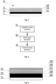
- Fig. 1 schematically illustrates the optoelectronic foil in a cross-section, showing the layered foil construction.
- the optoelectronic foil has a substrate 11 with a barrier layer 12 on which a conductive layer 13 comprising at least one oxide layer 131 and at least one metal layer 132 is deposited.
- the substrate 11 of the optoelectronic foil 10 may be made of a variety of transparent substrate materials selected from the group consisting of plastics and/or plastics with nanocomposites of inorganic materials.
- plastics for the substrate 11 may be provided in the form of at least one type of material selected from the group consisting of polyethylene terephthalate (PET), polyethylene naphthalene (PEN), polyethylene (PE), polypropylene (PP), polyethersulfone (PES), polyimide (PI), polystyrene (PS), ethylene/tetrafluoroethylene (ETFE) and polymers evaporated onto the surface from the group of poly-p-xylenes collectively referred to as parylene.
- PET polyethylene terephthalate
- PEN polyethylene naphthalene
- PE polyethylene
- PP polypropylene
- PES polyethersulfone
- PI polyimide
- PS polystyrene
- EFE ethylene/tetrafluoro
- the barrier layer 12 of the foil 10 has a barrier function and prevents against moisture and oxygen penetration from the substrate 11 into the conductive layer 13, thus ensuring a significant reduction of degradation processes of the conductive layer that constitutes the optoelectronic element of the foil 10 and of the active layers of the device that can be deposited onto the optoelectronic foil 10.
- the barrier layer 12 consists of at least one material selected from the group consisting of silicon oxides (SiO x ), aluminium oxides (Al 2 O 3 , AlO x N y ), titanium oxides (TiO x ), silicon oxynitrides SiON, silicon nitrides (Si 3 N 4 , SiN x ), organic silicon compounds (SiC x H y ), zirconium oxide (ZrO 2 ), hafnium oxide (HfO 2 ), chromium oxides (CrO, Cr 2 O 3 , CrO 2 , CrO 3 , CrO 5 ) and parylene.
- the barrier layer may consist of at least two different materials selected from the group consisting of silicon oxides (SiO x ), aluminium oxides (Al 2 O 3 , AlO x N y ), titanium oxides (TiO x ), silicon oxynitride SiON, silicon nitrides (Si 3 N 4 , SiN x ), organic silicon compounds (SiC x H y ), zirconium oxide (ZrO 2 ), hafnium oxide (HfO 2 ), chromium oxides (CrO, Cr 2 O 3 , CrO 2 , CrO 3 , CrO 5 ) and parylene.
- silicon oxides SiO x
- aluminium oxides Al 2 O 3 , AlO x N y
- titanium oxides TiO x
- silicon oxynitride SiON silicon nitrides
- Si 3 N 4 silicon nitrides
- SiN x organic silicon compounds
- ZrO 2 zirconium oxide
- the barrier layer may take, for example, the form of a monolayer consisting of only one material, such as Al 2 O 3 .
- the barrier layer may take the form of a monolayer comprising at least two different materials and may be made, for example, of Al 2 O 3 doped with TiO 2 .
- the barrier layer 12 may consist of at least two different materials, and it may take the form of a multi-layer comprising, within the barrier layer 12, at least two sub-layers stacked one on the other, wherein each sub-layer may be made of different material or materials.
- the barrier layer may have two sublayers, where one sublayer is made of Al 2 O 3 , and the other sublayer is made of TiO 2 .
- Each sublayer within the barrier layer 12 may be of the same or different thickness, preferably in the range between 5 and 500 nm, regardless of the thickness of another sublayer.
- the barrier layer 12 may comprise two sublayers, each made of a different material, selected from the group of materials listed above.
- the barrier layer 12 may have a total thickness preferably in the range between 5 and 1000 nm.
- the conductive layer 13 is an optoelectronic active layer of the foil with conductive properties.
- the conductive layer 13 comprises at least one oxide layer 131, 133 and at least one metal layer 132 stacked one on the other.
- the conductive layer comprises at least two oxide layers 131 and 133, or more than two oxide layers, separated by metal layers 132 to form a sandwich architecture. All layers 131, 132, 133 are stacked in the conductive layer 13 one on the other, substantially in parallel.
- the oxide layer 131, 133 is made of at least one oxide selected from the group consisting of: ZnO, AZO (aluminium zinc oxide), SnO 2 , IZO (indium zinc oxide), FTO (fluorine tin oxide), ZTO (tin zinc oxide), ITO (tin indium oxide), GZO (zinc gallium oxide), GIO (indium gallium oxide), In 2 O 3 , Sb:SnO 2 , IO:H (hydrogen indium oxide), CdO, Zn 2 SnO 4 , ZnSnO 3 , Zn 2 In 2 O 5 , NiO x , NiO x :Li, TiO x , ZnS, ZnSe, Te 2 O 3 , MoO x , V 2 O 5 and WO 3 .
- the oxide layer 13 of the optoelectronic foil 10 the oxide selected from the group consisting of: ZnO, AZO (aluminium zinc oxide), SnO 2
- the oxide layer 131, 133 may take the form of a monolayer and consist of one type of oxide, from the group of oxides listed above, for example ZnO.
- the oxide layer may take the form of a monolayer and consist of more than one material, for example the oxide layer 131, 133, in the form of a monolayer may be made of ZnO doped with Al.
- the oxide layer 131, 133 may consist of at least two different oxides and may take the form of a multilayer comprising, within one oxide layer 131, 133, at least two sublayers, wherein each sublayer is made of a different oxide material comprising at least one oxide.
- the oxide layer 131, 133 may consist of two sublayers stacked one on the other within one oxide layer 131, 133, wherein one sublayer is made of ZnO and the other sublayer is made of AZO or IZTO doped with Al.
- the optoelectronic foil may comprise at least two oxide layers 131, 133, wherein one oxide layer takes the form of a monolayer and another oxide layer takes the form of a multilayer comprising at least two sublayers made of different oxide materials.
- the metal layer 132 is made of at least one metal selected from the group consisting of: Al, Ti, Ni, Cr, Au, Mg, Ta, Ge, Ag, Cu, Zr, Pt and W.
- the metal layer 132 may preferably have a thickness in the range between 2 and 20 nm.
- the conductive layer 13 may comprise, as schematically shown in Fig. 1 , two oxide layers 131, 133, each of which may be a multi- or monolayer, and one metal layer 132 separating the two oxide layers.
- the conductive layer 13 may have three oxide layers and two metal layers stacked within the conductive layer one alternately on the other, so that each of the metal layers separates the two adjacent oxide layers.
- the conductive layer may have n oxide layers 131, 133, each of which may be a multi- or monolayer, and n-1 metal layers stacked one on the other, so that each metal layer 132 separates two adjacent oxide layers 132, 133 forming a sandwich structure, where n is any number selected from the set of natural numbers.
- n may be 2, 3, 4, 5, 6 or 7.
- n may be up to 33, or n may be more than 33.
- Fig. 2 schematically shows a manufacturing method of the optoelectronic foil.
- a substrate material 11 is prepared in order to produce the optoelectronic foil in step 21.
- the preparation process involves thorough cleaning and activation of the selected substrate surface.
- the cleaning and activation process of step 21 is implemented using at least one technique selected from the group consisting of plasma treatment, corona discharge treatment, carbon dioxide treatment, cleaning with solvents such as acetone, isopropanol, water, or mixtures of acetone and water or a mixture of isopropanol and water, as well as surface treatment with ultraviolet (UV) radiation and ozone.
- a barrier layer 12 is deposited onto the cleaned and activated surface of the substrate 11.
- step 22 may include one or more steps.
- the barrier layer may be deposited in one step.
- the deposition step 22 may comprise several sub-steps, each involving depositing one sublayer onto the barrier layer 12.
- the deposition in step 22 is implemented so that a sublayer of one material is deposited in the first step, and then a sublayer of another material selected from the material group for the barrier layer 12 listed above is deposited.
- the processes of depositing the barrier layer 12 having both the structure of a multilayer and monolayer may be implemented using at least one known deposition technique selected from the group consisting of: atomic layer deposition (ALD) technique, magnetron sputtering technique, electron-beam sputtering technique and thermal evaporation technique.
- ALD atomic layer deposition
- a conductive layer 13 is deposited onto the barrier layer having a multi- or monolayer structure, wherein each of the sublayers of the conductive layer 13, that is at least two oxide layers 131, 132 and at least one metal layer 132, is deposited onto the barrier layer 12 individually, in order to obtain the appropriate functionality and architecture of the conductive layer 13, e.g. a sandwich architecture.
- Each of the sublayers 131, 132, 133 of the conductive layer can be deposited using various deposition methods also known from the art, selected from the group consisting of: atomic layer deposition (ALD) technique, magnetron sputtering, electron-beam sputtering technique and thermal evaporation technique.
- ALD atomic layer deposition
- Each of the sub-layers 131, 132, 133 may be deposited using the same or different deposition techniques.
- the oxide layer 131, 133 may be deposited in step 23 in single step or several steps, each of which may be implemented using one technique as well as different deposition techniques.
- the oxide layer 131, 133 may be deposited in single step 23.
- the oxide layer may be deposited in several steps in step 23, each step including depositing one sublayer within the oxide layer 131, 133.
- the optoelectronic foil obtained combines barrier properties and an efficient conductive layer 13, which preferably may have the architecture of an electrode, depending on the materials used as the materials for oxide and metal layers 131, 132, 133, respectively.
- the conductive layer 13 is integrated with an flexible substrate 11, 12 having barrier properties.
- the barrier layer of the optoelectronic foil has water vapor permeability rates (WVTR) ranging between 10 -3 and 10 -6 g/m 2 per day and has stable barrier properties, including high hydrophobicity and UV radiation resistance, which improves the lifespan of the conductive layer of the foil according to the present invention.
- WVTR water vapor permeability rates
- the optoelectronic foil is flexible and is characterised by relatively high transparency, while the conductive layer of the foil has good conductivity and is an alternative to the single, thicker conductive ITO (indium tin oxide) layer known in the prior art that is relatively brittle, has limited conductivity and is expensive.
- ITO indium tin oxide
- the optoelectronic foil according to one embodiment of the present invention is schematically shown as a cross-section in Fig. 1 .
- the optoelectronic foil comprises a substrate 11, which in this embodiment is made of a plastic, namely polyethylene terephthalate (PET).
- PET polyethylene terephthalate
- the top surface of substrate 11 was cleaned and activated using oxygen plasma treatment.
- a single barrier layer 12 made of AlO x with a thickness of 300 nm, which is an amorphous layer was deposited onto the top surface of substrate 11 thus prepared in the reactive magnetron sputtering process.
- a conductive layer 13 was deposited onto the barrier layer 12 in the reactive magnetron sputtering process, comprising the first oxide layer 131 made of ITO with a thickness of 20 nm, a metal layer 132 made of Ag with a thickness of 9 nm and a second oxide layer 133 made of ITO with a thickness of 20 nm.
- the tests conducted yielded a surface resistance of the conductive layer 13 of 12 ⁇ / ⁇ , a WVTR permeability rate of 10 -3 g/m 2 per day and light transmission in the visible spectrum in the range of 70-78%.
- the optoelectronic foil according to another embodiment of the present invention is schematically shown as a cross-section in Fig. 3 .
- the optoelectronic foil comprises a substrate 11, which in this embodiment is made of a plastic, namely polyethylene terephthalate (PET).
- PET polyethylene terephthalate
- the top surface of substrate 11 was cleaned and activated using oxygen plasma treatment.
- a barrier layer 12 in the form of an AlO x layer 121 with a thickness of 100 nm and a TiO x layer 122 with a thickness of 150 nm, which constitute amorphous layers, were deposited onto the top surface of substrate 11 thus prepared in the reactive magnetron sputtering process.
- a conductive layer 13 was deposited onto the barrier layer 12 in the reactive magnetron sputtering process, containing the first oxide layer 131 made of ITO with a thickness of 20 nm, a metal layer 132 made of Ag with a thickness of 9 nm and a second oxide layer 133 made of ITO with a thickness of 20 nm.
- the tests conducted yielded a surface resistance of the conductive layer 13 of 12 ⁇ / ⁇ , a WVTR permeability rate of less than 5*10 -4 g/m 2 per day and light transmission in the visible spectrum in the range of 67-80%.
Description
- The present invention relates to an optoelectronic foil and a method for the production thereof.
- In terms of design, the optoelectronic foil consists of a flexible polymer foil substrate and a transparent electrode. It is the basis for the construction of a wide array of optoelectronic devices that are produced on said foils using a variety of techniques. Optoelectronic devices, for the construction of which optoelectronic foils are used, include flexible emission displays (OLED, QD LCD), flexible photovoltaic devices, touch screen sensors, flexible random access memory (RAM) and gas sensors.
- The disadvantage of optoelectronic flexible foils lies in the poor tightness of the flexible substrate constituted by polymer foils with a high oxygen and water permeability coefficient, which result in the short lifespan of optoelectronic devices. Especially devices containing organic materials in active layers, for example OLEDs (Organic Light Emitting Diodes) are sensitive to weather conditions. Moisture and oxygen penetration from the air cause the degradation of the active material, which, as a result, precludes the optoelectronic device from operating.
- Various technologies are known for the production of protective layers in the structure of optoelectronic foils designed to extend the lifespan of optoelectronic devices, including:
- "Dam-and-fill" encapsulation technique. During this process, a high viscosity fluid is distributed, forming a rectangular barrier around the device (e.g. an OLED). Said fluid is distributed during the droplet application process so as to fill the space between the substrate and the barrier film within the barrier. This method is characterized by simplicity and high stability;
- technique of sealing using a thin multi-layer foil, i.e. "thin-film-encapsulation" (TFE). The most common TFE technologies include plasma-enhanced chemical vapor deposition (PECVD) and atomic layer deposition (ALD);
- Plasma-enhanced chemical vapor deposition (PECVD) involves preparation of an inorganic-and-inorganic or organic-and-organic barrier, with the process typically using silicon nitride or silicon dioxide; the advantage of this technique lies in the low temperature process (below 600°C), and the possibility of deposition of nonequilibrium phases, as well as the relatively high purity of the resulting coatings;
- atomic layer deposition technique, (ALD), which involves depositing a barrier film; this technique uses e.g. aluminium oxides and nitrides for deposition; the advantage of this method is that it allows for obtaining coatings characterised by relatively good tightness.
- Moreover, some techniques that are known for improving barrier characteristics and general sealing of a FOLED (Flexible Organic Light Emitting Diode) display, involve using ultra-thin metal or glass foils. The advantage of this type of solutions is the achievement of foils with good gas permeability properties, while it is their disadvantage that the foils obtained are matte, opaque and easily damaged.
- Further, patent literature discloses structures of conductive materials used for the construction of optoelectronic devices.
- International patent application
WO2015/179834A1 discloses a structure of a conductive film consisting of silver (Ag) in an amount of no less than 80% of the total atomic content of the conductive film and a conductive metal selected from the group consisting of: Al, Ti, Ni, Cr, Au, Mg, Ta, Ge in an amount of no more than 20% of the total atomic content of the conductive film. The manufacturing process of the electrically conductive layer comprises the co-deposition of gold, copper and a conductive metal on a substrate to form a continuous conductive film.WO2015/179834A1 , however, does not provide information on the method for preparing a barrier layer to limit the moisture or oxygen penetration into the conductive film. Examples of structures disclosing a substrate, a barrier layer and a conductive layer are disclosed in patent publicationsEP2871681A1 andUS2014/054578A1 . - Therefore, it is desirable to provide a flexible optoelectronic foil structure with improved barrier properties against particles of gas and water vapour, which would allow for the manufacture of optoelectronic devices with an extended lifespan without deterioration of the transparency of the entire foil material. It is also desirable to provide the optoelectronic foil, which would be useful for both, passive devices incorporating barrier solutions and active optoelectronic devices including flexible, transparent electrodes.
- The invention relates to an optoelectronic foil and a method for manufacturing an optoelectronic foil according to the appended claims.
- An embodiment of the present invention will now be described by way of example with reference to the accompanying drawings, wherein:
-
Fig. 1 schematically shows a cross-section of the structure of an optoelectronic foil according to one embodiment of the present invention; -
Fig. 2 shows a flowchart of the optoelectronic foil manufacturing process, and -
Fig. 3 schematically shows a cross-section of the structure of an optoelectronic foil according to another embodiment of the present invention. - The optoelectronic foil according to the invention has a transparency of no less than 50% and is characterised by low water vapor permeability, as the water vapor transmission rate (WVTR) of the
optoelectronic foil 10 is between 10-3 and 10-6 g/m2 per day. Due to optoelectronic properties and high transparency, the foil can be used for the manufacture of various devices, including, but not limited to, devices from the field of imaging optoelectronics and photovoltaic optoelectronics. For example, the foil can be used for the manufacture of flexible OLED or QD LCD displays, in photovoltaic systems, including, but not limited to, ultra-thin, transparent photovoltaic cells that can be placed on window panes, computer screens, mobile phones, clothing parts, and other everyday use items. Due to improved barrier properties and improved lifespan, the foil can also be used in the automotive or construction industry. -
Fig. 1 schematically illustrates the optoelectronic foil in a cross-section, showing the layered foil construction.
The optoelectronic foil has asubstrate 11 with abarrier layer 12 on which aconductive layer 13 comprising at least oneoxide layer 131 and at least onemetal layer 132 is deposited. - The
substrate 11 of theoptoelectronic foil 10 may be made of a variety of transparent substrate materials selected from the group consisting of plastics and/or plastics with nanocomposites of inorganic materials. For example, plastics for thesubstrate 11 may be provided in the form of at least one type of material selected from the group consisting of polyethylene terephthalate (PET), polyethylene naphthalene (PEN), polyethylene (PE), polypropylene (PP), polyethersulfone (PES), polyimide (PI), polystyrene (PS), ethylene/tetrafluoroethylene (ETFE) and polymers evaporated onto the surface from the group of poly-p-xylenes collectively referred to as parylene. - The
barrier layer 12 of thefoil 10 has a barrier function and prevents against moisture and oxygen penetration from thesubstrate 11 into theconductive layer 13, thus ensuring a significant reduction of degradation processes of the conductive layer that constitutes the optoelectronic element of thefoil 10 and of the active layers of the device that can be deposited onto theoptoelectronic foil 10. - The
barrier layer 12 consists of at least one material selected from the group consisting of silicon oxides (SiOx), aluminium oxides (Al2O3, AlOxNy), titanium oxides (TiOx), silicon oxynitrides SiON, silicon nitrides (Si3N4, SiNx), organic silicon compounds (SiCxHy), zirconium oxide (ZrO2), hafnium oxide (HfO2), chromium oxides (CrO, Cr2O3, CrO2, CrO3, CrO5) and parylene. More preferably, the barrier layer may consist of at least two different materials selected from the group consisting of silicon oxides (SiOx), aluminium oxides (Al2O3, AlOxNy), titanium oxides (TiOx), silicon oxynitride SiON, silicon nitrides (Si3N4, SiNx), organic silicon compounds (SiCxHy), zirconium oxide (ZrO2), hafnium oxide (HfO2), chromium oxides (CrO, Cr2O3, CrO2, CrO3, CrO5) and parylene. - In one embodiment, the barrier layer may take, for example, the form of a monolayer consisting of only one material, such as Al2O3. In another embodiment, the barrier layer may take the form of a monolayer comprising at least two different materials and may be made, for example, of Al2O3 doped with TiO2. In yet another embodiment, the
barrier layer 12 may consist of at least two different materials, and it may take the form of a multi-layer comprising, within thebarrier layer 12, at least two sub-layers stacked one on the other, wherein each sub-layer may be made of different material or materials. For example, the barrier layer may have two sublayers, where one sublayer is made of Al2O3, and the other sublayer is made of TiO2. Each sublayer within thebarrier layer 12 may be of the same or different thickness, preferably in the range between 5 and 500 nm, regardless of the thickness of another sublayer. - Preferably, the
barrier layer 12 may comprise two sublayers, each made of a different material, selected from the group of materials listed above. Thebarrier layer 12 may have a total thickness preferably in the range between 5 and 1000 nm. - The
conductive layer 13 is an optoelectronic active layer of the foil with conductive properties. Theconductive layer 13 comprises at least oneoxide layer metal layer 132 stacked one on the other. - Moreover, as shown in
Fig. 1 , the conductive layer comprises at least twooxide layers metal layers 132 to form a sandwich architecture. Alllayers conductive layer 13 one on the other, substantially in parallel. - In each embodiment of the
conductive layer 13, comprising more than one, for example twooxide layers oxide layer conductive layer 13 of theoptoelectronic foil 10, theoxide layer - In one embodiment, the
oxide layer oxide layer oxide layer oxide layer oxide layer oxide layer - Depending on the intended use and the required parameters, the optoelectronic foil may comprise at least two
oxide layers conductive layer 13 comprising more than one oxide layer, themetal layer 132 is made of at least one metal selected from the group consisting of: Al, Ti, Ni, Cr, Au, Mg, Ta, Ge, Ag, Cu, Zr, Pt and W. For each embodiment of theconductive layer 13 of theoptoelectronic foil 10, themetal layer 132 may preferably have a thickness in the range between 2 and 20 nm. - Depending on the target utility parameters of the optoelectronic foil, the
conductive layer 13 may comprise, as schematically shown inFig. 1 , twooxide layers metal layer 132 separating the two oxide layers. In another embodiment, theconductive layer 13 may have three oxide layers and two metal layers stacked within the conductive layer one alternately on the other, so that each of the metal layers separates the two adjacent oxide layers. In yet another embodiment, the conductive layer may have n oxide layers 131, 133, each of which may be a multi- or monolayer, and n-1 metal layers stacked one on the other, so that eachmetal layer 132 separates twoadjacent oxide layers -
Fig. 2 schematically shows a manufacturing method of the optoelectronic foil. - A
substrate material 11 is prepared in order to produce the optoelectronic foil instep 21. The preparation process involves thorough cleaning and activation of the selected substrate surface. The cleaning and activation process ofstep 21 is implemented using at least one technique selected from the group consisting of plasma treatment, corona discharge treatment, carbon dioxide treatment, cleaning with solvents such as acetone, isopropanol, water, or mixtures of acetone and water or a mixture of isopropanol and water, as well as surface treatment with ultraviolet (UV) radiation and ozone. - Then, in
step 22, abarrier layer 12 is deposited onto the cleaned and activated surface of thesubstrate 11. - Depending on the structure of the
barrier layer 12,step 22 may include one or more steps. For example, in order to form a barrier layer having a monolayer structure and made of at least one type of material, for example Al2O3, or Al2O3 doped with TiO2, instep 22 the barrier layer may be deposited in one step. However, in order to form a barrier layer with a multilayer structure comprising at least two sublayers made of different materials, thedeposition step 22 may comprise several sub-steps, each involving depositing one sublayer onto thebarrier layer 12. For example, to form a barrier layer comprising two sublayers, the deposition instep 22 is implemented so that a sublayer of one material is deposited in the first step, and then a sublayer of another material selected from the material group for thebarrier layer 12 listed above is deposited. The processes of depositing thebarrier layer 12 having both the structure of a multilayer and monolayer may be implemented using at least one known deposition technique selected from the group consisting of: atomic layer deposition (ALD) technique, magnetron sputtering technique, electron-beam sputtering technique and thermal evaporation technique. - Then, in
step 23, aconductive layer 13 is deposited onto the barrier layer having a multi- or monolayer structure, wherein each of the sublayers of theconductive layer 13, that is at least twooxide layers metal layer 132, is deposited onto thebarrier layer 12 individually, in order to obtain the appropriate functionality and architecture of theconductive layer 13, e.g. a sandwich architecture. Each of thesublayers - For example, the
conductive layer 13 having the architecture, as shown inFig. 1 , comprising twooxide layers metal layer 132 between the oxide layers, is deposited instep 23 so that in the first step, thefirst oxide layer 131 is deposited directly onto the surface of thebarrier layer 12, then ametal layer 132 is deposited onto the first oxide layer, and then asecond oxide layer 133 is deposited onto themetal layer 132. Each of thesub-layers - Furthermore, depending on the target structure of the oxide layers 131, 133, each of which may take the form of a monolayer or a multilayer, the
oxide layer step 23 in single step or several steps, each of which may be implemented using one technique as well as different deposition techniques. For example, for anoxide layer oxide layer single step 23. Now, in order to form theoxide layer step 23, each step including depositing one sublayer within theoxide layer - The optoelectronic foil obtained combines barrier properties and an efficient
conductive layer 13, which preferably may have the architecture of an electrode, depending on the materials used as the materials for oxide andmetal layers foil 10, theconductive layer 13 is integrated with anflexible substrate - The barrier layer of the optoelectronic foil has water vapor permeability rates (WVTR) ranging between 10-3 and 10-6 g/m2 per day and has stable barrier properties, including high hydrophobicity and UV radiation resistance, which improves the lifespan of the conductive layer of the foil according to the present invention.
- Moreover, the optoelectronic foil is flexible and is characterised by relatively high transparency, while the conductive layer of the foil has good conductivity and is an alternative to the single, thicker conductive ITO (indium tin oxide) layer known in the prior art that is relatively brittle, has limited conductivity and is expensive.
- The optoelectronic foil according to one embodiment of the present invention is schematically shown as a cross-section in
Fig. 1 . The optoelectronic foil comprises asubstrate 11, which in this embodiment is made of a plastic, namely polyethylene terephthalate (PET). The top surface ofsubstrate 11 was cleaned and activated using oxygen plasma treatment. Then, asingle barrier layer 12 made of AlOx with a thickness of 300 nm, which is an amorphous layer, was deposited onto the top surface ofsubstrate 11 thus prepared in the reactive magnetron sputtering process. Next, aconductive layer 13 was deposited onto thebarrier layer 12 in the reactive magnetron sputtering process, comprising thefirst oxide layer 131 made of ITO with a thickness of 20 nm, ametal layer 132 made of Ag with a thickness of 9 nm and asecond oxide layer 133 made of ITO with a thickness of 20 nm. The optoelectronic foil thus obtained was subjected to tests involving a measurement of surface resistance by means of a four-point probe, a WVTR permeability measurement by means of a calcium test (measurement conditions RH=40%, T = 25°C) and measurement of light transmission in the visible spectrum using a UV-Vis spectrophotometer. The tests conducted yielded a surface resistance of theconductive layer 13 of 12 Ω/□, a WVTR permeability rate of 10-3 g/m2 per day and light transmission in the visible spectrum in the range of 70-78%. - The use of a three-layer electrode structure (conductive layer 13), where the two
oxide layers thin metal layer 132, provided high flexibility to the conductive layer 13 (due to the presence of the metal layer 12), and, as a result, to the entire optoelectronic foil, together with high conductivity are ensured, as demonstrated in the tests described above. - The optoelectronic foil according to another embodiment of the present invention is schematically shown as a cross-section in
Fig. 3 . The optoelectronic foil comprises asubstrate 11, which in this embodiment is made of a plastic, namely polyethylene terephthalate (PET). The top surface ofsubstrate 11 was cleaned and activated using oxygen plasma treatment. Then, abarrier layer 12 in the form of an AlOx layer 121 with a thickness of 100 nm and a TiOx layer 122 with a thickness of 150 nm, which constitute amorphous layers, were deposited onto the top surface ofsubstrate 11 thus prepared in the reactive magnetron sputtering process. Next, aconductive layer 13 was deposited onto thebarrier layer 12 in the reactive magnetron sputtering process, containing thefirst oxide layer 131 made of ITO with a thickness of 20 nm, ametal layer 132 made of Ag with a thickness of 9 nm and asecond oxide layer 133 made of ITO with a thickness of 20 nm. The optoelectronic foil thus obtained was subjected to tests involving a measurement of surface resistance by means of a four-point probe, a WVTR permeability measurement by means of a calcium test (measurement conditions RH=40%, T = 25°C) and measurement of light transmission in the visible spectrum using a UV-Vis spectrophotometer. The tests conducted yielded a surface resistance of theconductive layer 13 of 12 Ω/□, a WVTR permeability rate of less than 5*10-4 g/m2 per day and light transmission in the visible spectrum in the range of 67-80%.
Claims (15)
- An optoelectronic foil comprising a substrate (11) and a conductive layer (13) comprising at least one metal layer (132), wherein:between the conductive layer (13) and the substrate (11), the foil (10) comprises a barrier layer (12) comprising at least one material selected from the group consisting of silicon oxides (SiOx), aluminium oxides (Al2O3, AlOxNy), titanium oxides (TiOx), silicon oxynitrides SiON, silicon nitrides (Si3N4, SiNx), organic silicon compounds (SiCxHy), zirconium oxide (Zr02), hafnium oxide (HfO2), chromium oxides (CrO, Cr2O3, CrO2, CrO3, CrO5) and parylene,characterized in that the conductive layer (13) further comprises n oxide layers (131, 133) and n-1 metal layers (132), wherein the layers (131, 133, 132) are stacked one on the other, so that each metal layer (132) separates two adjacent oxide layers (132, 133) forming a sandwich structure, wherein n is a natural number not less than 2,wherein each oxide layer (131, 133) is made of at least one oxide selected from the group consisting of: ZnO, AZO (aluminium zinc oxide), SnO2, IZO (indium zinc oxide), FTO (fluorine tin oxide), ZTO (tin zinc oxide), ITO (tin indium oxide), GZO (zinc gallium oxide), GIO (indium gallium oxide), In2O3, Sb:SnO2, IO:H (hydrogen indium oxide), CdO, Zn2SnO4, ZnSnO3, Zn2In2O5, NiOx, NiOx:Li, TiOx, ZnS, ZnSe, Te2O3, MoOx, V2O5 and WO3,and wherein at least one of the oxide layers (131, 133) is:- either a monolayer structure- or a multi-layer structure consisting of at least two sublayers stacked one on the other within the oxide layer (131, 133) and wherein one of the sublayers is made of a different material than another sublayer.
- The optoelectronic foil according to claim 1 characterised in that the barrier layer (12) is a monolayer structure.
- The optoelectronic foil according to claim 1 , characterised in that the barrier layer (12) is a multi-layer structure consisting of at least two sublayers stacked one on the other within the barrier layer (12) and wherein one of the sublayers is made of a different material than another sublayer.
- The optoelectronic foil according to any of the claims 1 to 3, characterised in that the substrate (1 1 ) is made of at least one plastic selected from the group consisting of: polyethylene terephthalate (PET), polyethylene naphthalene (PEN), polyethylene (PE), polypropylene (PP), polyethersulfone (PES), polyimide (PI), polystyrene (PS), ethylene/tetrafluoroethylene (ETFE) and parylene.
- The optoelectronic foil according to claim 4, characterised in that the substrate (11 ) is doped with inorganic nanocomposites.
- The optoelectronic foil according to any of the claims 1 to 5, characterised in that the metal layer (132) is made of a material selected from the group consisting of: Al, Ti, Ni, Cr, Au, Mg, Ta, Ge, Ag, Cu, Zr, Pt and W.
- The optoelectronic foil according to any of the claims 1 to 6, characterised in that the conductive layer (13), comprises n oxide layers (131, 133) and n-1 metal layers (132) arranged alternately between adjacent oxide layers (131, 133).
- A method for manufacturing the optoelectronic foil of claim 1 comprising the steps of:- cleaning and activating a selected surface of the substrate onto which a barrier layer (12) is to be deposited,- forming the barrier layer (12) on said cleaned and activated substrate (11),- and, after forming the barrier layer (12), forming a conductive layer (13) comprising deposition of at least one metal layer (132) wherein- the step of forming the barrier layer (12) comprises depositing of at least one material selected from the group consisting of silicon oxides (SiOx), aluminium oxides (Al2O3, AlOxNy), titanium oxides (TiOx), silicon oxynitrides SiON, silicon nitrides (Si3N4, SiNx), organic silicon compounds (SiCxHy), zirconium oxide (ZrO2), hafnium oxide (HfO2), chromium oxides (CrO, Cr2O3, CrO2, CrO3, CrOs) and parylene,
characterized in that- the step of forming the conductive layer (13) further comprises depositing of at least two adjacent metal oxide layers (131, 133) each comprising at least one oxide selected from the group consisting of: ZnO, AZO (aluminum zinc oxide), SnO2, IZO (indium zinc oxide), FTO (fluorine tin oxide), ZTO (tin zinc oxide), ITO (tin indium oxide), GZO (zinc gallium oxide), GIO (indium gallium oxide), In2O3, Sb:SnO2, IO:H (hydrogen indium oxide), CdO, Zn2SnO4, ZnSnO3, Zn2ln2O5, NiOx, NiOx:Li, TiOx, ZnS, ZnSe, Te2O3, MoOx, V2O5 and WO3, and wherein depositing of the metal layer (132) comprises depositing of a single layer of metal selected from the group consisting of: Al, Ti, Ni, Cr, Au, Mg, Ta, Ge, Ag, Cu, Zr, Pt and W,wherein forming the conductive layer (13) comprises forming on the barrier layer (12) consecutively: the first oxide layer (131), the single metal layer (132) and the second oxide layer (133). - The method according to claim 8, characterised in that the barrier layer (12) is formed by depositing one layer of material onto the substrate (11) to form a barrier layer (12) having a monolayer structure.
- The method according to claim 8 or 9, characterised in that the barrier layer (12) is formed by depositing at least two sublayers of different material onto the substrate (11) to form the barrier layer (12) having a multi-layer structure.
- The method according to any of the claims 8 to 10, characterised in that the conductive layer (13) is formed so that on the barrier layer (12) there are individually formed one on another, with the alternating arrangement of oxide layers (131 , 133) and metal layers (132), n oxide layers (131, 133) and n-1 metal layers (132), where n is a natural number.
- The method according to any of the claims 8 to 11, characterised in that at least one oxide layer (131, 133) is formed by depositing one layer of oxide material to form an oxide layer (131, 133) having a monolayer structure.
- The method according to any of the claims 8 to 11, characterised in that at least one oxide layer (131 , 133) is formed by depositing at least two oxide sublayers of different material to form an oxide layer (12) having a multi-layer structure.
- The method according to any of the claims 8 to 13 , characterised in that the substrate (11) is cleaned and activated using at least one technique selected from the group consisting of: plasma treatment, corona discharge treatment, carbon dioxide treatment, ultraviolet radiation and ozone treatment, and cleaning with solvents selected from the group consisting of acetone, isopropanol, water, mixture of acetone and water and mixture of isopropanol and water.
- The method according to any of the claims 8 to 14, characterised in that the barrier layer (12) and the conductive layer (13) are independently deposited onto the substrate (11) using at least one technique selected from the group consisting of atomic layer deposition (ALD), magnetron sputtering, electron-beam sputtering technique and thermal evaporation technique.
Applications Claiming Priority (2)
| Application Number | Priority Date | Filing Date | Title |
|---|---|---|---|
| PL420300A PL233211B1 (en) | 2017-01-25 | 2017-01-25 | Optoelectronic film and method for producing optoelectronic film |
| PCT/PL2018/000008 WO2018139945A1 (en) | 2017-01-25 | 2018-01-24 | Optoelectronic foil and manufacturing method of optoelectronic foil |
Publications (2)
| Publication Number | Publication Date |
|---|---|
| EP3574528A1 EP3574528A1 (en) | 2019-12-04 |
| EP3574528B1 true EP3574528B1 (en) | 2024-03-13 |
Family
ID=61683865
Family Applications (1)
| Application Number | Title | Priority Date | Filing Date |
|---|---|---|---|
| EP18711714.8A Active EP3574528B1 (en) | 2017-01-25 | 2018-01-24 | Optoelectronic foil and manufacturing method of optoelectronic foil |
Country Status (7)
| Country | Link |
|---|---|
| US (1) | US20190348621A1 (en) |
| EP (1) | EP3574528B1 (en) |
| JP (1) | JP7206559B2 (en) |
| CN (1) | CN110291647B (en) |
| FI (1) | FI3574528T3 (en) |
| PL (1) | PL233211B1 (en) |
| WO (1) | WO2018139945A1 (en) |
Families Citing this family (7)
| Publication number | Priority date | Publication date | Assignee | Title |
|---|---|---|---|---|
| PL425218A1 (en) * | 2018-04-13 | 2019-10-21 | Centrum Badań I Rozwoju Technologii Dla Przemysłu Spółka Akcyjna | Silicon photovoltaic cell and method for producing silicon photovoltaic cells |
| CN109979977A (en) | 2019-03-28 | 2019-07-05 | 武汉华星光电半导体显示技术有限公司 | OLED display panel and preparation method thereof |
| KR20220090558A (en) * | 2020-02-04 | 2022-06-29 | 미쓰이금속광업주식회사 | Metal foil with carrier |
| CN111638610A (en) * | 2020-07-20 | 2020-09-08 | 宁波材料所杭州湾研究院 | Flexible intelligent light adjusting film with high visible light transmittance and heat insulation and preparation method thereof |
| JP7230131B2 (en) * | 2020-09-04 | 2023-02-28 | デクセリアルズ株式会社 | Conductive laminate, optical device using same, method for manufacturing conductive laminate |
| EP4209341A1 (en) * | 2020-09-04 | 2023-07-12 | Dexerials Corporation | Conductive layered product, optical device using same, and manufacturing method for conductive layered product |
| EP4064378B1 (en) | 2021-03-23 | 2024-03-06 | Saule S.A. | A light-transmissive multilayer structure for optoelectronic devices |
Citations (1)
| Publication number | Priority date | Publication date | Assignee | Title |
|---|---|---|---|---|
| WO2012029780A1 (en) * | 2010-09-03 | 2012-03-08 | 大日本印刷株式会社 | Solar cell and solar cell module |
Family Cites Families (13)
| Publication number | Priority date | Publication date | Assignee | Title |
|---|---|---|---|---|
| JPH1024520A (en) * | 1996-07-11 | 1998-01-27 | Mitsui Petrochem Ind Ltd | Transparent conductive laminate |
| JP3862466B2 (en) | 2000-02-29 | 2006-12-27 | 三井化学株式会社 | Transparent electrode |
| JP4742584B2 (en) | 2004-03-23 | 2011-08-10 | 株式会社豊田中央研究所 | electrode |
| US8252624B2 (en) * | 2010-01-18 | 2012-08-28 | Applied Materials, Inc. | Method of manufacturing thin film solar cells having a high conversion efficiency |
| FR2973946B1 (en) * | 2011-04-08 | 2013-03-22 | Saint Gobain | ELECTRONIC LAYER DEVICE |
| WO2012169845A2 (en) * | 2011-06-10 | 2012-12-13 | 주식회사 포스코 | Solar cell substrate, method for manufacturing same, and solar cell using same |
| KR101642589B1 (en) * | 2013-09-30 | 2016-07-29 | 주식회사 엘지화학 | Substrate for organic electronic device and manufacturing method thereof |
| EP2871681A1 (en) * | 2013-11-07 | 2015-05-13 | Saint-Gobain Glass France | Back contact substrate for a photovoltaic cell or module |
| JP2016103443A (en) | 2014-11-28 | 2016-06-02 | パイオニア株式会社 | Light-emitting device |
| JP5994884B2 (en) | 2015-03-03 | 2016-09-21 | コニカミノルタ株式会社 | ORGANIC ELECTROLUMINESCENT ELEMENT AND LIGHTING DEVICE |
| CN106158901B (en) | 2015-03-24 | 2020-06-23 | 上海和辉光电有限公司 | Hybrid film, preparation method thereof and flexible OLED display |
| US10573856B2 (en) * | 2015-05-14 | 2020-02-25 | GM Global Technology Operations LLC | Barrier layer coatings for battery pouch cell seal |
| US10836959B2 (en) * | 2015-05-26 | 2020-11-17 | Toray Industries, Inc. | Pyrromethene-boron complex, color-changing composition, color-changing film, light source unit including same, display, and lighting |
-
2017
- 2017-01-25 PL PL420300A patent/PL233211B1/en unknown
-
2018
- 2018-01-24 JP JP2019539927A patent/JP7206559B2/en active Active
- 2018-01-24 FI FIEP18711714.8T patent/FI3574528T3/en active
- 2018-01-24 WO PCT/PL2018/000008 patent/WO2018139945A1/en unknown
- 2018-01-24 CN CN201880008575.4A patent/CN110291647B/en active Active
- 2018-01-24 EP EP18711714.8A patent/EP3574528B1/en active Active
-
2019
- 2019-07-25 US US16/521,645 patent/US20190348621A1/en active Pending
Patent Citations (1)
| Publication number | Priority date | Publication date | Assignee | Title |
|---|---|---|---|---|
| WO2012029780A1 (en) * | 2010-09-03 | 2012-03-08 | 大日本印刷株式会社 | Solar cell and solar cell module |
Also Published As
| Publication number | Publication date |
|---|---|
| CN110291647B (en) | 2024-03-26 |
| JP7206559B2 (en) | 2023-01-18 |
| PL420300A1 (en) | 2018-07-30 |
| JP2020505736A (en) | 2020-02-20 |
| US20190348621A1 (en) | 2019-11-14 |
| FI3574528T3 (en) | 2024-04-23 |
| EP3574528A1 (en) | 2019-12-04 |
| PL233211B1 (en) | 2019-09-30 |
| CN110291647A (en) | 2019-09-27 |
| WO2018139945A1 (en) | 2018-08-02 |
Similar Documents
| Publication | Publication Date | Title |
|---|---|---|
| EP3574528B1 (en) | Optoelectronic foil and manufacturing method of optoelectronic foil | |
| US8766280B2 (en) | Protective substrate for a device that collects or emits radiation | |
| US9059425B2 (en) | Multilayer electronic device having one or more barrier stacks | |
| EP3001428B1 (en) | Conductive film and electronic device having conductive film | |
| JP2020505736A5 (en) | ||
| KR101809296B1 (en) | Transparent electode and electronic device comprising the same | |
| KR20140106567A (en) | Translucent gas barrier film, method for producing translucent gas barrier film, organic el element, solar cell, and thin-film cell | |
| CN106887274A (en) | A kind of flexible transparent conductive film and preparation method thereof | |
| US9704610B2 (en) | Manganese tin oxide based transparent conducting oxide and transparent conductive film and method for fabricating transparent conductive film using the same | |
| EP4064378B1 (en) | A light-transmissive multilayer structure for optoelectronic devices | |
| KR20160020834A (en) | Barrier film structure and organic electronic device having the same | |
| KR101816972B1 (en) | Transparent electrode with TiO2/Ag/TiO2 multilayered structure and method for preparing the same | |
| KR20170021619A (en) | Transparent electrode with AZO/Ag/AZO mulilayered structure and method for preparing the same | |
| CN113614926A (en) | Transparent multilayer component and method of manufacture |
Legal Events
| Date | Code | Title | Description |
|---|---|---|---|
| STAA | Information on the status of an ep patent application or granted ep patent |
Free format text: STATUS: UNKNOWN |
|
| STAA | Information on the status of an ep patent application or granted ep patent |
Free format text: STATUS: THE INTERNATIONAL PUBLICATION HAS BEEN MADE |
|
| PUAI | Public reference made under article 153(3) epc to a published international application that has entered the european phase |
Free format text: ORIGINAL CODE: 0009012 |
|
| STAA | Information on the status of an ep patent application or granted ep patent |
Free format text: STATUS: REQUEST FOR EXAMINATION WAS MADE |
|
| 17P | Request for examination filed |
Effective date: 20190823 |
|
| AK | Designated contracting states |
Kind code of ref document: A1 Designated state(s): AL AT BE BG CH CY CZ DE DK EE ES FI FR GB GR HR HU IE IS IT LI LT LU LV MC MK MT NL NO PL PT RO RS SE SI SK SM TR |
|
| AX | Request for extension of the european patent |
Extension state: BA ME |
|
| RAP1 | Party data changed (applicant data changed or rights of an application transferred) |
Owner name: SAULE SPOLKA AKCYJNA |
|
| DAV | Request for validation of the european patent (deleted) | ||
| DAX | Request for extension of the european patent (deleted) | ||
| STAA | Information on the status of an ep patent application or granted ep patent |
Free format text: STATUS: EXAMINATION IS IN PROGRESS |
|
| 17Q | First examination report despatched |
Effective date: 20200528 |
|
| STAA | Information on the status of an ep patent application or granted ep patent |
Free format text: STATUS: EXAMINATION IS IN PROGRESS |
|
| GRAP | Despatch of communication of intention to grant a patent |
Free format text: ORIGINAL CODE: EPIDOSNIGR1 |
|
| STAA | Information on the status of an ep patent application or granted ep patent |
Free format text: STATUS: GRANT OF PATENT IS INTENDED |
|
| RIC1 | Information provided on ipc code assigned before grant |
Ipc: H10K 50/816 20230101ALI20231012BHEP Ipc: H10K 30/82 20230101ALI20231012BHEP Ipc: H10K 102/10 20230101ALI20231012BHEP Ipc: H01L 31/0392 20060101ALI20231012BHEP Ipc: H01L 31/0224 20060101AFI20231012BHEP |
|
| INTG | Intention to grant announced |
Effective date: 20231031 |
|
| GRAS | Grant fee paid |
Free format text: ORIGINAL CODE: EPIDOSNIGR3 |
|
| GRAA | (expected) grant |
Free format text: ORIGINAL CODE: 0009210 |
|
| STAA | Information on the status of an ep patent application or granted ep patent |
Free format text: STATUS: THE PATENT HAS BEEN GRANTED |
|
| RAP3 | Party data changed (applicant data changed or rights of an application transferred) |
Owner name: SAULE SPOLKA AKCYJNA |
|
| AK | Designated contracting states |
Kind code of ref document: B1 Designated state(s): AL AT BE BG CH CY CZ DE DK EE ES FI FR GB GR HR HU IE IS IT LI LT LU LV MC MK MT NL NO PL PT RO RS SE SI SK SM TR |
|
| REG | Reference to a national code |
Ref country code: GB Ref legal event code: FG4D |
|
| REG | Reference to a national code |
Ref country code: CH Ref legal event code: EP |
|
| REG | Reference to a national code |
Ref country code: DE Ref legal event code: R096 Ref document number: 602018066536 Country of ref document: DE |
|
| P01 | Opt-out of the competence of the unified patent court (upc) registered |
Effective date: 20240301 |
|
| REG | Reference to a national code |
Ref country code: SE Ref legal event code: TRGR |