EP3563406B1 - Iodine-containing compounds for etching semiconductor structures - Google Patents
Iodine-containing compounds for etching semiconductor structures Download PDFInfo
- Publication number
- EP3563406B1 EP3563406B1 EP17889218.8A EP17889218A EP3563406B1 EP 3563406 B1 EP3563406 B1 EP 3563406B1 EP 17889218 A EP17889218 A EP 17889218A EP 3563406 B1 EP3563406 B1 EP 3563406B1
- Authority
- EP
- European Patent Office
- Prior art keywords
- iodine
- etching
- silicon
- layer
- reaction chamber
- Prior art date
- Legal status (The legal status is an assumption and is not a legal conclusion. Google has not performed a legal analysis and makes no representation as to the accuracy of the status listed.)
- Active
Links
Images


Classifications
-
- H—ELECTRICITY
- H01—ELECTRIC ELEMENTS
- H01L—SEMICONDUCTOR DEVICES NOT COVERED BY CLASS H10
- H01L21/00—Processes or apparatus adapted for the manufacture or treatment of semiconductor or solid state devices or of parts thereof
- H01L21/02—Manufacture or treatment of semiconductor devices or of parts thereof
- H01L21/04—Manufacture or treatment of semiconductor devices or of parts thereof the devices having potential barriers, e.g. a PN junction, depletion layer or carrier concentration layer
- H01L21/18—Manufacture or treatment of semiconductor devices or of parts thereof the devices having potential barriers, e.g. a PN junction, depletion layer or carrier concentration layer the devices having semiconductor bodies comprising elements of Group IV of the Periodic Table or AIIIBV compounds with or without impurities, e.g. doping materials
- H01L21/30—Treatment of semiconductor bodies using processes or apparatus not provided for in groups H01L21/20 - H01L21/26
- H01L21/31—Treatment of semiconductor bodies using processes or apparatus not provided for in groups H01L21/20 - H01L21/26 to form insulating layers thereon, e.g. for masking or by using photolithographic techniques; After treatment of these layers; Selection of materials for these layers
- H01L21/3105—After-treatment
- H01L21/311—Etching the insulating layers by chemical or physical means
- H01L21/31105—Etching inorganic layers
- H01L21/31111—Etching inorganic layers by chemical means
- H01L21/31116—Etching inorganic layers by chemical means by dry-etching
-
- H—ELECTRICITY
- H01—ELECTRIC ELEMENTS
- H01L—SEMICONDUCTOR DEVICES NOT COVERED BY CLASS H10
- H01L21/00—Processes or apparatus adapted for the manufacture or treatment of semiconductor or solid state devices or of parts thereof
- H01L21/02—Manufacture or treatment of semiconductor devices or of parts thereof
- H01L21/04—Manufacture or treatment of semiconductor devices or of parts thereof the devices having potential barriers, e.g. a PN junction, depletion layer or carrier concentration layer
- H01L21/18—Manufacture or treatment of semiconductor devices or of parts thereof the devices having potential barriers, e.g. a PN junction, depletion layer or carrier concentration layer the devices having semiconductor bodies comprising elements of Group IV of the Periodic Table or AIIIBV compounds with or without impurities, e.g. doping materials
- H01L21/30—Treatment of semiconductor bodies using processes or apparatus not provided for in groups H01L21/20 - H01L21/26
- H01L21/302—Treatment of semiconductor bodies using processes or apparatus not provided for in groups H01L21/20 - H01L21/26 to change their surface-physical characteristics or shape, e.g. etching, polishing, cutting
- H01L21/306—Chemical or electrical treatment, e.g. electrolytic etching
- H01L21/3065—Plasma etching; Reactive-ion etching
-
- H—ELECTRICITY
- H01—ELECTRIC ELEMENTS
- H01L—SEMICONDUCTOR DEVICES NOT COVERED BY CLASS H10
- H01L21/00—Processes or apparatus adapted for the manufacture or treatment of semiconductor or solid state devices or of parts thereof
- H01L21/02—Manufacture or treatment of semiconductor devices or of parts thereof
- H01L21/04—Manufacture or treatment of semiconductor devices or of parts thereof the devices having potential barriers, e.g. a PN junction, depletion layer or carrier concentration layer
- H01L21/18—Manufacture or treatment of semiconductor devices or of parts thereof the devices having potential barriers, e.g. a PN junction, depletion layer or carrier concentration layer the devices having semiconductor bodies comprising elements of Group IV of the Periodic Table or AIIIBV compounds with or without impurities, e.g. doping materials
- H01L21/30—Treatment of semiconductor bodies using processes or apparatus not provided for in groups H01L21/20 - H01L21/26
- H01L21/302—Treatment of semiconductor bodies using processes or apparatus not provided for in groups H01L21/20 - H01L21/26 to change their surface-physical characteristics or shape, e.g. etching, polishing, cutting
- H01L21/306—Chemical or electrical treatment, e.g. electrolytic etching
- H01L21/308—Chemical or electrical treatment, e.g. electrolytic etching using masks
- H01L21/3083—Chemical or electrical treatment, e.g. electrolytic etching using masks characterised by their size, orientation, disposition, behaviour, shape, in horizontal or vertical plane
- H01L21/3085—Chemical or electrical treatment, e.g. electrolytic etching using masks characterised by their size, orientation, disposition, behaviour, shape, in horizontal or vertical plane characterised by their behaviour during the process, e.g. soluble masks, redeposited masks
-
- H—ELECTRICITY
- H01—ELECTRIC ELEMENTS
- H01L—SEMICONDUCTOR DEVICES NOT COVERED BY CLASS H10
- H01L21/00—Processes or apparatus adapted for the manufacture or treatment of semiconductor or solid state devices or of parts thereof
- H01L21/02—Manufacture or treatment of semiconductor devices or of parts thereof
- H01L21/04—Manufacture or treatment of semiconductor devices or of parts thereof the devices having potential barriers, e.g. a PN junction, depletion layer or carrier concentration layer
- H01L21/18—Manufacture or treatment of semiconductor devices or of parts thereof the devices having potential barriers, e.g. a PN junction, depletion layer or carrier concentration layer the devices having semiconductor bodies comprising elements of Group IV of the Periodic Table or AIIIBV compounds with or without impurities, e.g. doping materials
- H01L21/30—Treatment of semiconductor bodies using processes or apparatus not provided for in groups H01L21/20 - H01L21/26
- H01L21/31—Treatment of semiconductor bodies using processes or apparatus not provided for in groups H01L21/20 - H01L21/26 to form insulating layers thereon, e.g. for masking or by using photolithographic techniques; After treatment of these layers; Selection of materials for these layers
- H01L21/3105—After-treatment
- H01L21/311—Etching the insulating layers by chemical or physical means
- H01L21/31144—Etching the insulating layers by chemical or physical means using masks
-
- H—ELECTRICITY
- H01—ELECTRIC ELEMENTS
- H01L—SEMICONDUCTOR DEVICES NOT COVERED BY CLASS H10
- H01L21/00—Processes or apparatus adapted for the manufacture or treatment of semiconductor or solid state devices or of parts thereof
- H01L21/02—Manufacture or treatment of semiconductor devices or of parts thereof
- H01L21/04—Manufacture or treatment of semiconductor devices or of parts thereof the devices having potential barriers, e.g. a PN junction, depletion layer or carrier concentration layer
- H01L21/18—Manufacture or treatment of semiconductor devices or of parts thereof the devices having potential barriers, e.g. a PN junction, depletion layer or carrier concentration layer the devices having semiconductor bodies comprising elements of Group IV of the Periodic Table or AIIIBV compounds with or without impurities, e.g. doping materials
- H01L21/30—Treatment of semiconductor bodies using processes or apparatus not provided for in groups H01L21/20 - H01L21/26
- H01L21/31—Treatment of semiconductor bodies using processes or apparatus not provided for in groups H01L21/20 - H01L21/26 to form insulating layers thereon, e.g. for masking or by using photolithographic techniques; After treatment of these layers; Selection of materials for these layers
- H01L21/3205—Deposition of non-insulating-, e.g. conductive- or resistive-, layers on insulating layers; After-treatment of these layers
- H01L21/321—After treatment
- H01L21/3213—Physical or chemical etching of the layers, e.g. to produce a patterned layer from a pre-deposited extensive layer
- H01L21/32133—Physical or chemical etching of the layers, e.g. to produce a patterned layer from a pre-deposited extensive layer by chemical means only
- H01L21/32135—Physical or chemical etching of the layers, e.g. to produce a patterned layer from a pre-deposited extensive layer by chemical means only by vapour etching only
- H01L21/32136—Physical or chemical etching of the layers, e.g. to produce a patterned layer from a pre-deposited extensive layer by chemical means only by vapour etching only using plasmas
- H01L21/32137—Physical or chemical etching of the layers, e.g. to produce a patterned layer from a pre-deposited extensive layer by chemical means only by vapour etching only using plasmas of silicon-containing layers
-
- H—ELECTRICITY
- H10—SEMICONDUCTOR DEVICES; ELECTRIC SOLID-STATE DEVICES NOT OTHERWISE PROVIDED FOR
- H10B—ELECTRONIC MEMORY DEVICES
- H10B12/00—Dynamic random access memory [DRAM] devices
-
- H—ELECTRICITY
- H10—SEMICONDUCTOR DEVICES; ELECTRIC SOLID-STATE DEVICES NOT OTHERWISE PROVIDED FOR
- H10B—ELECTRONIC MEMORY DEVICES
- H10B41/00—Electrically erasable-and-programmable ROM [EEPROM] devices comprising floating gates
- H10B41/20—Electrically erasable-and-programmable ROM [EEPROM] devices comprising floating gates characterised by three-dimensional arrangements, e.g. with cells on different height levels
-
- H—ELECTRICITY
- H10—SEMICONDUCTOR DEVICES; ELECTRIC SOLID-STATE DEVICES NOT OTHERWISE PROVIDED FOR
- H10B—ELECTRONIC MEMORY DEVICES
- H10B43/00—EEPROM devices comprising charge-trapping gate insulators
- H10B43/20—EEPROM devices comprising charge-trapping gate insulators characterised by three-dimensional arrangements, e.g. with cells on different height levels
- H10B43/23—EEPROM devices comprising charge-trapping gate insulators characterised by three-dimensional arrangements, e.g. with cells on different height levels with source and drain on different levels, e.g. with sloping channels
- H10B43/27—EEPROM devices comprising charge-trapping gate insulators characterised by three-dimensional arrangements, e.g. with cells on different height levels with source and drain on different levels, e.g. with sloping channels the channels comprising vertical portions, e.g. U-shaped channels
-
- H—ELECTRICITY
- H10—SEMICONDUCTOR DEVICES; ELECTRIC SOLID-STATE DEVICES NOT OTHERWISE PROVIDED FOR
- H10D—INORGANIC ELECTRIC SEMICONDUCTOR DEVICES
- H10D1/00—Resistors, capacitors or inductors
Definitions
- the method includes the steps of introducing the vapor of an iodine-containing etching compound into a reaction chamber containing the silicon-containing film on a substrate.
- the iodine-containing etching compound iodine-containing etching compound is selected from the group comprising C 2 H 2 FI, C 2 H 3 F 2 I, C 2 H 4 FI, C 3 HF 4 I, C 3 H 2 F 3 I, C 3 HF 6 I, C 3 H 2 F 5 I, C 3 H 3 F 4 I, and C 3 H 4 F 3 I; or combinations thereof.
- An inert gas is introduced into the reaction chamber.
- a plasma is activated to produce an activated iodine-containing etching compound capable of etching the silicon-containing film from the substrate.
- plasma etching removes silicon-containing films, such as silicon oxide or silicon nitride layers, from semiconductor substrates.
- DRAM and 2D NAND are exemplary memory applications.
- etching of stacks of multiple SiO/SiN or SiO/poly-Silicon (p-Si) layers is critical. See, e.g., US 2011/0180941 to Samsung Electronics Co. , Ltd.
- An etchant having high selectivity between the mask and layers being etched is essential.
- the etched structure should have a straight vertical profile without bowing and low line etch roughness (LER).
- etch gases include octafluorocyclobutane ( C C 4 F 8 ), hexafluoro-1,3-butadiene (C 4 F 6 ), CF 4 , CH 2 F 2 , CH 3 F, and/or CHF 3 . It is well known that selectivity and polymer deposition rate increase as the ratio of C:F increases ( i.e ., C 4 F 6 > C 4 F 8 > CF 4 ). See, e.g., US6387287 to Hung et al .
- inert gases like Ar, Kr, or Xe
- Ar, Kr, or Xe are added to the plasma where they are ionized and accelerated to the wafer surface bombarding the surface and supporting the etching process. Because they are inert gases, they do not directly participate in the chemical reactions of the etching process.
- etch chemistries may not be able to provide a feature, such as a hole or trench, having an aspect ratio higher than 20:1, which is necessary in the newer applications (e.g., 3D NAND), at least due to insufficient etch resistant polymer deposition on sidewalls during the plasma etching processes.
- the sidewall - C x F y - polymers, wherein x ranges from 0.01 to 1 and y ranges from 0.01 to 4 may be susceptible to etching.
- the etched patterns may not be vertical and the etch structures may show bowing, change in dimensions, pattern collapse and/or increased roughness.
- Bowing may result from sidewall etching of the mask layer, which may often be an amorphous carbon (a-C) material.
- the a-C materials may be etched by oxygen radicals in the plasma which may cause increased opening of the mask and result in bow-like, or angled/curved, etch structures.
- Iodine-containing compounds have been used as etching gases.
- Chung US Pat. No. 9,460,935 discloses etching first and second etching layers under plasma generated using, among others, 1,1,2,2-tetrafluoro-1-iodoethane. See also Karecki et al., Plasma etching of dielectric films with novel iodofluorocarbon chemistries: iodotrifluoroethylene and 1-iodoheptafluoropropane, J. Vac. Sci. Technol. A 16, 755 (1998 ); JP2006/108484 to Ulvac ; TWI343601 to Ulvac.
- etching today has not been limited to selectivity to the photoresist mask. It is equally important to get high selectivity among other materials such as a-C, SiN, p-Si, SiC or other forms of Si a C b O c H d N e materials (where a>0; b, c, d and e ⁇ 0).
- the methods include the steps of: introducing a vapor of an iodine-containing etching compound into a reaction chamber containing a silicon-containing film on a substrate, wherein the iodine-containing etching is selected from the group consisting of C 2 H 2 FI, C 2 H 3 F 2 I, C 2 H 4 FI, C 3 HF 4 I, C 3 H 2 F 3 I, C 3 HF 6 I, C 3 H 2 F 5 I, C 3 H 3 F 4 I, and C 3 H 4 F 3 I; introducing an inert gas into the reaction chamber; and activating a plasma to produce an activated iodine-containing etching compound capable of etching the silicon-containing film from the substrate.
- the disclosed methods include one or more of the following aspects:
- the disclosed iodine-containing etching compounds include one or more of the following aspects:
- Table 1 a or an one or more than one approximately or about ⁇ 10% of the value stated LCD-TFT liquid-crystal display-thin-film transistor DRAM dynamic random-access memory FinFET fin-shaped field-effect transistor Bulk CMOS Bulk complementary metal-oxide-semiconductor FD-SOI fully depleted silicon-on-insulator FEOL front end of the line BEOL back end of the line TSV through silicon via RIE reactive ion etching CCP capacitively coupled plasma ICP inductively coupled plasma Sccm standard cubic centimeters per minute Slm standard liter per minute ONON silicon oxide and silicon nitride alternating layers TCAT terabit cell array transistor P-BICS pipe-shaped bit cost scalable QMS Quadrupole mass spectrometer ARC or BARC Anti-reflecting coating or Bottom anti-reflecting coating a-C amorphous carbon CAS chemical abstract service PCTFE Polychlorotrifluoroethene PVDF polyvinylidene fluor
- etch means to use a plasma to remove material via ion bombardment, remote plasma, or chemical vapor reaction between the etching gas and substrate.
- the etch process may be anisotropic or isotropic.
- plasma dry etching process produces anisotropic etching; chemical etching or wet etching process produces isotropic etching.
- the etching process may be used to produce apertures, such as vias, trenches, channel holes, gate trenches, staircase contacts, capacitor holes, contact holes, etc., in the substrate.
- pattern etch or “patterned etch” refers to etching a non-planar structure, such as a patterned mask layer on a stack of silicon-containing films.
- mask refers to a layer that resists etching.
- the mask layer may be located above the layer to be etched.
- etch stop layer refers to a layer below the layer to be etched that protects layers underneath.
- device channel refers to layers that are part of actual device and any damage to it will affect device performance.
- the term "aspect ratio” refers to a ratio of the height of a trench (or via) to the width of the trench (or the diameter of the via).
- selectivity means the ratio of the etch rate of one material to the etch rate of another material.
- selective etch or “selectively etch” means to etch one material more than another material, or in other words to have a greater or less than 1:1 etch selectivity between two materials.
- R groups independently selected relative to other R groups bearing the same or different subscripts or superscripts, but is also independently selected relative to any additional species of that same R group.
- R groups may, but need not be identical to each other or to R 2 or to R 3 .
- values of R groups are independent of each other when used in different formulas.
- film and “layer” may be used interchangeably. It is understood that a film may correspond to, or related to a layer, and that the layer may refer to the film. Furthermore, one of ordinary skill in the art will recognize that the terms “film” or “layer” used herein refer to a thickness of some material laid on or spread over a surface and that the surface may range from as large as the entire wafer to as small as a trench or a line.
- etching compound and “etching gas” may be used interchangeably. It is understood that an etching compound may correspond to, or related to an etching gas, and that the etching gas may refer to the etching compound.
- the abbreviation "2D” refers to 2 dimensional gate structures on a planar substrate;
- the abbreviation “3D” refers to 3 dimensional or vertical gate structures, wherein the gate structures are stacked in the vertical direction.
- the silicon-containing films such as silicon nitride and silicon oxide, are listed throughout the specification and claims without reference to their proper stoichoimetry.
- the silicon-containing films may include pure silicon (Si) layers, such as crystalline Si, poly-silicon (p-Si or polycrystalline Si), or amorphous silicon; silicon nitride (Si k N l ) layers; or silicon oxide (Si n O m ) layers; or mixtures thereof, wherein k, I, m, and n, inclusively range from 0.1 to 6.
- silicon nitride is Si k N l , where k and I each range from 0.5 to 1.5. More preferably silicon nitride is Si 3 N 4 .
- silicon oxide is Si n O m , where n ranges from 0.5 to 1.5 and m ranges from 1.5 to 3.5. More preferably, silicon oxide is SiO 2 .
- SiN and SiO in the following description are used to represent Si k N l and Si n O m containing layers, respectively.
- the silicon-containing film could also be a silicon oxide based dielectric material such as organic based or silicon oxide based low- k dielectric materials such as the Black Diamond II or III material by Applied Materials, Inc. with a formula of SiOCH. Silicon-containing film may also include Si a O b N c where a, b, c range from 0.1 to 6.
- the silicon-containing films may also include dopants, such as B, C, P, As and/or Ge.
- the disclosed methods include the steps of i) introducing a vapor of an iodine-containing etching compound into a reaction chamber containing a silicon-containing film on a substrate, wherein the iodine-containing etching compound is is selected from the group as defined in the claims; ii) introducing an inert gas into the reaction chamber; and iii) activating a plasma to produce an activated iodine-containing etching compound capable of etching the silicon-containing film from the substrate.
- the iodide ion of the disclosed iodine-containing etching compounds dissociates from the compounds at low energies (eV)( i.e ., ⁇ 20 eV).
- eV low energies
- the disclosed etching compounds may be used in dry plasma etch processes that produce less damage to the underlying substrates because they can be performed at lower plasma energies.
- the disclosed iodine-containing etching compounds may be particularly suitable for low k etch processes in which damage is a particular concern because lower plasma energy may produce less damage to the porous low k material surrounding the etch site.
- the disclosed iodine-containing etching compounds may also prevent loss of the critical dimension and decrease low k surface roughness.
- molecules with two iodine atoms may enhance these benefits, although at a loss of volatility due to the size of the iodine atoms.
- Iodine (10.5eV) has a lower ionization threshold than Fluorine (17.4eV) and the inert gases: Ar (15.8eV), Xe (12.1eV), and Kr (14eV). Iodine may therefore be more easily ionized by the plasma than fluorine. Iodine may also behave similarly to the inert gases in the plasma and accelerate towards the wafer. Fluorine's ionization threshold serves to maintain it as a neutral species. As a result, fluorine typically participates in the etching process via chemical reactions. Iodine exhibits less chemical reactivity than fluorine and is ionized and bombards the surface during the plasma etch process. The bond energy for C-I is also less than the bond energy for C-F, thereby causing the C-I bond to more easily break in the plasma compared to C-F bonds.
- the iodide ion dissociates from the disclosed etching compounds at low eVs (i.e., ⁇ 20 eV).
- the resulting iodide ion may be too large to enter features having narrow widths or diameters.
- iodide ion implantation into the mask feature is likely. This implantation may help to strengthen the mask feature and help it maintain its shape during the etching process.
- iodine-containing etching compounds are listed in Table 2. These molecules are commercially available or may be synthesized by methods known in the art. Their structure formula, CAS numbers and boiling points are included in Table 2. Table 2. Commercially available etching compounds Etching compounds Formula Structure CAS number Boiling point (°C)* Trifluoroiodo-methane CF 3 I 2314-97-8 -22.5 Difluorodiiodo-methane CF 2 I 2 1184-76-5 ⁇ 89 Difluoroiodo-methane CHF 2 I 1493-03-4 21.6 Fluoroiodomethane CH 2 FI 373-53-5 53.4 1,1,2-trifluoro-2-iodo-ethene C 2 F 3 I 359-37-5 30 1,2-difluoro-1-iodo-ethene (1E)-1,2-difluoro-1-iodo-ethene C 2 HF 2 I 2925-16-8 183106-80-1 35.5
- Exemplary non-claimed compounds include CF 2 I 2 . Applicants believe that the etch rate of SiN may be enhanced while maintaining high selectivity to the mask layer when the disclosed iodine-containing etching compounds include at least one H.
- the molecules having 2-3 carbon atoms may provide better sidewall protection during the etching process than the C1 molecules.
- C3 molecules are preferred because Applicants believe they will produce thicker passivation layers.
- Exemplary C3 iodine-containing etching compounds include C 3 H 2 F 5 I, C 3 H 3 F 4 I, or C 3 H 4 F 3 I, even more preferably, C 3 H 2 F 3 I, or C 3 H 4 F 3 I;
- Exemplary C2 iodine-containing etching compounds include C 2 H 2 FI, C 2 H 3 F 2 I, C 2 H 4 FI. and more preferably 1,1-difluoro-1-iodo-ethane.
- the etch rate of SiN may be enhanced while maintaining high selectivity to the mask layer when the disclosed iodine-containing etching compounds include at least one H, thus being C 2 H 2 FI, C 2 H 4 FI, C 3 HF 4 I, C 3 H 2 F 3 I, C 3 HF 6 I, C 3 H 2 F 5 I, C 3 H 3 F 4 I, and C 3 H 4 F 3 I.
- the C3 molecules are preferred for sidewall protection and include C 3 HF 4 I, C 3 H 2 F 3 I, C 3 H 3 F 4 I, and C 3 H 4 F 3 I.
- the C2 molecules may be easier to deliver to the reactor. and include C 2 H 2 FI, C 2 H 3 F 2 I, and more preferably 1,1-difluoro-1-iodo-ethane.
- the disclosed iodine-containing etching compounds may provide high selectivity to mask layers, etch stop layers and device channel materials and no profile distortion in high aspect ratio structures, such as those having an aspect ratio ranging from 10:1 to 200:1 such as DRAM and 3D NAND applications.
- the disclosed iodine-containing etching compounds may also provide high selectivity to mask layers or silicon nitride, such as those having an aspect ratio ranging from 1:1 to 50:1 in contact etch applications.
- the disclosed iodine-containing etching compounds may provide infinite selectivity for wide process conditions of etching.
- the selectivity refers to the etching rate ratio of two different layers.
- the selectivity for SiO layer vs. a-C layer is the etch rate of the SiO divided by the etching rate of the a-C layer.
- the disclosed iodine-containing etching compounds may provide improved selectivity between the silicon-containing films and mask materials, less damage to channel region, and reduced bowing in pattern high aspect ratio structures.
- the disclosed iodine-containing etching compounds may also etch through alternating layers of p-Si, SiO, and/or SiN, resulting in a vertical etch profile (i.e., demonstrating selectivity ranging from 2:1 to 1:2 between the alternating layers).
- the disclosed iodine-containing etching compounds are provided at greater than 95% v/v purity, preferably at greater than 99.99% v/v purity, and more preferably at greater than 99.999% v/v purity.
- the disclosed iodine-containing etching compounds contain less than 5% by volume trace gas impurities, with less than 150 ppm by volume of impurity gases, such as N 2 and/or H 2 O and/or CO 2 , contained in said trace gaseous impurities.
- the water content in the plasma etching gas is less than 20 ppmw by weight.
- the purified product may be produced by distillation and/or passing the gas or liquid through a suitable adsorbent, such as a 4A molecular sieve.
- the disclosed iodine-containing etching compounds contain less than 10% v/v, preferably less than 1% v/v, more preferably less than 0.1% v/v, and even more preferably less than 0.01% v/v of any of its isomers, which may be purified by distillation of the gas or liquid to remove isomers and may provide better process repeatability.
- the disclosed iodine-containing etching compounds may contain between 5% v/v and 50% v/v of its isomers, particularly when the isomer mixture provides improved process parameters or if isolation of the target isomer is too difficult or expensive.
- the disclosed iodine-containing etching compounds may comprise between approximately 50% v/v and approximately 75% v/v (1E)-1,2-difluoro-1-iodo-ethene and between approximately 25% v/v and approximately 50% v/v (1Z)-1,2-difluoro-1-iodo-ethene.
- the mixture of isomers may also reduce the need for two or more gas lines to the reaction chamber.
- Some of the disclosed iodine-containing etching compounds are gaseous at room temperature and atmospheric pressure.
- the non-gaseous (i.e., liquid or solid) compounds their gas form may be produced by vaporizing the compounds through a conventional vaporization step, such as direct vaporization or by bubbling with inert gas (N 2 , Ar, He).
- the non-gaseous compounds may be fed in liquid state to a vaporizer where it is vaporized before it is introduced into a reactor.
- the disclosed iodine-containing etching compounds are suitable for plasma etching semiconductor structures, such as, channel holes, gate trenches, staircase contacts, capacitor holes, contact holes, etc., in the silicon-containing films.
- the disclosed iodine-containing etching compounds are not only compatible with currently available mask materials but also compatible with the future generations of mask materials because the disclosed iodine-containing etching compounds induce little to no damage on the mask along with good profile of high aspect ratio structures.
- the disclosed iodine-containing etching compounds may produce vertical etched patterns having minimal to no bowing, pattern collapse, or roughness.
- the disclosed iodine-containing etching compounds may deposit an etch-resistant polymer layer during etching to help reduce the direct impact of the oxygen and fluorine radicals during the etching process.
- the disclosed iodine-containing etching compounds may also reduce damage to p-Si or crystalline Si channel structure during etching.
- the disclosed iodine-containing etching compounds are suitably volatile and stable during the etching process for delivery into the reactor/chamber.
- Material compatibility tests are important to determine if any of the disclosed iodine-containing etching compounds will react with chamber materials and degrade the performance of the chamber with short term or long term use.
- Key materials involved in parts of the chamber, valves, etc. include stainless steel, aluminum, nickel, PCTFE, PVDF, PTFE and other metals and polymers. At times these materials are exposed to high temperatures, for example, higher than 20°C, and high pressures, for example, higher than 1 atm, which may enhance their degradation.
- the metrology methods may include visual inspection, weight measurement, measuring nanometer scale changes in scanning electron microscopy (SEM), tensile strength, hardness, etc.
- the disclosed iodine-containing etching compounds may be used to plasma etch silicon-containing films on a substrate.
- the disclosed plasma etching method may be useful in the manufacture of semiconductor devices such as NAND or 3D NAND gates or Flash or DRAM memory or transistors such as fin-shaped field-effect transistor (FinFET), Bulk complementary metal-oxide-semiconductor (Bulk CMOS), fully depleted silicon-on-insulator (FD-SOI) structures.
- the disclosed iodine-containing etching compounds may be used in other areas of applications, such as different front end of the line (FEOL) and back end of the line (BEOL) etch applications. Additionally, the disclosed iodine-containing etching compounds may also be used for etching Si in 3D through silicon via (TSV) etch applications for interconnecting memory to logic on a substrate.
- TSV silicon via
- the plasma etching method includes providing a reaction chamber having a substrate disposed therein.
- the reaction chamber may be any enclosure or chamber within a device in which etching methods take place such as, and without limitation, reactive ion etching (RIE), capacitively coupled plasma (CCP) with single or multiple frequency RF sources, inductively coupled plasma (ICP), or microwave plasma reactors, or other types of etching systems capable of selectively removing a portion of the silicon-containing film or generating active species.
- RIE reactive ion etching
- CCP capacitively coupled plasma
- ICP inductively coupled plasma
- microwave plasma reactors or other types of etching systems capable of selectively removing a portion of the silicon-containing film or generating active species.
- Suitable commercially available plasma reaction chambers include but are not limited to the Applied Materials magnetically enhanced reactive ion etcher sold under the trademark eMAX TM or the Lam Research Dual CCP reactive ion etcher dielectric etch product family sold under the trademark 2300 ® Flex TM .
- the RF power in such may be pulsed to control plasma properties and thereby improving the etch performance (selectivity and damage) further.
- the plasma-treated reactant may be produced outside of the reaction chamber.
- the MKS Instruments' ASTRONi ® reactive gas generator may be used to treat the reactant prior to passage into the reaction chamber.
- the reactant O 2 Operated at 2.45 GHz, 7kW plasma power, and a pressure ranging from approximately 0.5 Torr to approximately 10 Torr, the reactant O 2 may be decomposed into two O radicals.
- the remote plasma may be generated with a power ranging from about 1 kW to about 10 kW, more preferably from about 2.5 kW to about 7.5 kW.
- the reaction chamber may contain one or more than one substrate.
- the reaction chamber may contain from 1 to 200 silicon wafers having from 25.4 mm to 450 mm diameters.
- the substrates may be any suitable substrates used in semiconductor, photovoltaic, flat panel or LCD-TFT device manufacturing. Examples of suitable substrates include wafers, such as silicon, silica, glass, or GaAs wafers. The wafer will have multiple films or layers on it from previous manufacturing steps, including silicon-containing films or layers. The layers may or may not be patterned.
- suitable layers include without limitation silicon (such as amorphous silicon, p-Si, crystalline silicon, any of which may further be p-doped or n-doped with B, C, P, As, and/or Ge), silica, silicon nitride, silicon oxide, silicon oxynitride, Si a O b H c C d N e , (wherein a>0; b, c, d, e ⁇ 0) , mask layer materials such as amorphous carbon, antireflective coatings, photoresist materials, tungsten, titanium nitride, tantalum nitride or combinations thereof, etch stop layer materials such as silicon nitride, polysilicon, crystalline silicon, silicon carbide, SiCN or combinations thereof, device channel materials such crystalline silicon, epitaxial silicon, doped silicon, Si a O b H c C d N e , (wherein a>0; b, c, d,
- the silicon oxide layer may form a dielectric material, such as an organic based or silicon oxide based low-k dielectric material (e.g ., a porous SiCOH film).
- a dielectric material such as an organic based or silicon oxide based low-k dielectric material (e.g ., a porous SiCOH film).
- An exemplary low-k dielectric material is sold by Applied Materials under the trade name Black Diamond II or III.
- layers comprising tungsten or noble metals e.g. platinum, palladium, rhodium or gold
- examples of the silicon-containing films may be Si a O b H c C d N e , (wherein a>0; b, c, d, e ⁇ 0).
- the wafer and any associated layers thereon are referred to as substrates.
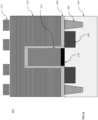
- a substrate 100 may include a stack of multiple layers as shown in FIG 1a.
- FIG. 1a is a cross-sectional side view of exemplary layers in a 3D NAND stack to produce a 3D NAND gate.
- a stack of seven alternative SiO/SiN (i.e ., 104a/104b) layers 104 is located on top of a silicon wafer 102 ( i.e ., ONON or TCAT technology).
- a silicon wafer 102 i.e ., ONON or TCAT technology.
- p-Si layers e.g. , SiO/p-Si or P-BICS technology.
- An amorphous carbon (a-C) mask layer 106 is located on the top of the seven SiO/SiN layers 104.
- the a-C mask layer 106 may contain C and H, as well as other elements, such as boron, nitrogen, etc., to improve etch resistance during SiO/SiN layer etch.
- An antireflective coating layer 108 is located on top of the a-C mask layer 106.
- a patterned photoresist layer 110 is located on top of the antireflective coating layer 108.
- a SiON layer (not shown) may be present between the antireflective coating layer 108 and the a-C mask layer 106 to transfer pattern in photoresist layer 110 to the a-C layer 106.
- the stack of layers in the substrate 100 in FIG. 1a is provided for exemplary purposes only and that the disclosed iodine-containing etching compounds may be used to etch other types of stacks of layers.
- the number alternating SiO/SiN or SiO/p-Si layers 104 in the stack of the substrate 100 may vary ( i.e., may include more or less than the seven SiO/SiN (104a/104b) layers depicted).
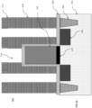
- FIG. 1b is a cross-sectional side view of the exemplary layers in the 3D NAND stack of FIG. 1a showing polymer deposited on a sidewall during etching.
- the disclosed iodine-containing etching compounds may produce fragments during the plasma process that are suitable for both anisotropically etching the silicon-containing films 104 and depositing an I-containing polymer passivation layer 212 on sidewalls of a structure being etched as shown in FIG. 1b .
- the difference between FIG. 1b and FIG. 1a is in FIG. 1b via 214 is formed in substrate 100 by plasma etching using the disclosed iodine-containing etch compounds, which also deposit the polymer passivation layer 212 on the sidewalls of the via 214 .
- the polymer passivation layer 212 also provides smoother sidewall, less bowing and less deformation at the bottom of the via 214.
- the polymer passivation layer 212 may however be easily removed or cleaned by dry or wet etch chemistries known in the art.
- FIG. 1c is a cross-sectional side view of the exemplary layers in the 3D NAND stack of FIG. 1a showing particles 316 generated during alternating SiO/SiN layer etching in a 3D NAND stack.
- the particles 316 generated on the sidewalls of the alternative SiO/SiN ( i.e ., 104a/104b) layers 104 as shown in FIG. 1c may be minimized by using the disclosed iodine-containing etching compounds.
- the difference between FIG. 1c and FIG. 1b is in FIG. 1c the alternative SiO/SiN exposed sidewall has particles 316 generated during plasma etching. Applicants do not believe that the disclosed iodine-containing etching compounds will generate the particles 316 shown in Fig. 1c .
- FIG. 1d is a cross-sectional side view of the exemplary layers in the 3D NAND stack of FIG. 1a showing selective isotropic etching of the SiN layers 104b exposed on the sidewall in the 3D NAND stack after the anisotropic etching process.
- the SiN exposed sidewall in stack 100 may be etched selectively as shown in FIG. 1d by using the disclosed iodine-containing etching compounds to selectively break the SiN bonds in the SiN layers 104b over the Si-O bond in the SiO layers 104a forming a selective sidewall SiN etch 418 on the stack of SiO/SiN layers 104 in the via 214.
- the difference between FIG. 1d and FIG. 1b is in FIG.
- the selective sidewall SiN etch 418 is performed by wet etching using mixtures with phosphoric acid. Replacing wet etch process with dry plasma etch processes is known to greatly improve the economics of semiconductor device fabrication process since wet etching requires moving the substrate to different wet etching equipments. With the disclosed methods, all etching, including the selective sidewall SiN etch of FIG. 1d , may be performed in one piece of etching equipment, which may reduce the cost of the semiconductor fabrication.
- substrate 100 may include a stack of multiple layers thereon as shown in FIG. 2.
- FIG. 2 is a cross-sectional side view of exemplary layers in a DRAM stack to produce a DRAM memory.
- a stack of four layers is located on top of a silicon wafer 102.
- An a-C mask layer 106 is located on top of a large SiO layer 104a.
- An antireflective coating layer 108 is located on top of the a-C mask 106.
- a pattern photoresist layer 110 is located on top of the antireflective coating 108.
- a SiON layer (not shown) may be present between the antireflective coating layer 108 and the a-C mask layer 106 to transfer pattern in photoresist layer 110 to the a-C layer 106.
- the stack of layers in FIG. 2 is provided for exemplary purposes only and that the disclosed iodine-containing etching compounds may be used to etch other stacks of layers, for example, for a stack where the a-C mask layer 106 is replaced with a TiN layer.
- the number of layers in the stack may vary (i.e., may include more or less than the layers depicted).
- FIG. 3a is a cross-sectional side view of exemplary layers showing photoresist pattern over SiO insulation layer surrounding a typical transistor device region to produce a transistor structure.
- Substrate 600 may include a stack of four layers surrounding a transistor gate electrode region supported on the Silicon wafer 602 as shown in FIG 3a .
- the transistor region shown in FIG. 3a includes two doped silicon regions 606 acting as source and drain.
- Transistor gate dielectric 614 is present underneath gate electrode 616.
- the whole transistor, i.e ., transistor gate dielectric 614 and gate electrode 616, is surrounded by a thin SiN layer 608 which may later act as etch stop layer during contact etch.
- Each transistor device region 616/606 is separated by SiO isolation regions 604 in the silicon wafer 602 to minimize electrical interference.
- layer 602 may be located on top of a silicon oxide layer of the Silicon on Insulator (SOI) wafer.
- SOI Silicon on Insulator
- Another SiO layer 610 is deposited on the transistor and used to insulate any metal contact to the transistor device regions 606.
- Photoresist mask 612 is used to pattern the SiO layer 610. Etching is performed using the disclosed iodine-containing etching compounds in plasma environment. The photoresist mask 612 serves as a template to etch the SiO layer 610 and etching is stopped on the SiN layer 608 as shown in FIG 3b .
- FIG. 3b is a cross-sectional side view of the exemplary layers of FIG. 3a after etching the SiO insulation layer.
- the difference between FIG.3b and FIG. 3a is in FIG. 3b vias 718 are formed in the SiO layer 610 through etching by the disclosed iodine-containing etching compounds.
- the SiO layer 610 may be etched with photoresist layer 612 as a mask layer.
- the mask layer may be any suitable photoresist mask materials, such as TiN, a-C and so on. The etching may be stopped at the underlying SiN layer 608.
- the disclosed iodine-containing etching compounds may also be used to etch the SiN layer 608 with different plasma conditions and different mixtures.
- the stack and geometry of layers in FIG. 3a and FIG. 3b is provided for exemplary purposes only and that the disclosed iodine-containing etching compounds may be used to etch other types of stacks of layers.
- the number of layers in the stack may vary ( i . e ., may include more or less than the four layers depicted).
- the vapor of the disclosed iodine-containing etching compounds is introduced into the reaction chamber containing the substrate and silicon-containing films.
- the vapor may be introduced to the chamber at a flow rate ranging from approximately 0.1 sccm to approximately 1 slm.
- the vapor may be introduced to the chamber at a flow rate ranging from approximately 5 sccm to approximately 50 sccm.
- the vapor may be introduced to the chamber at a flow rate ranging from approximately 25 sccm to approximately 250 sccm.
- the flow rate may vary from tool to tool.
- the disclosed iodine-containing etching compounds may be supplied either in neat form or in a blend with an inert gas, such as N 2 , Ar, He, Xe, etc, or solvent.
- the disclosed iodine-containing etching compounds may be present in varying concentrations in the blend.
- the vapor form of the iodine-containing etching compounds may be produced by vaporizing the neat or blended iodine-containing etching compound solution through a conventional vaporization step such as direct vaporization or by bubbling.
- the neat or blended iodine-containing etching compounds may be fed in liquid state to a vaporizer where it is vaporized before it is introduced into the reactor.
- the neat or blended iodine-containing etching compounds may be vaporized by passing a carrier gas into a container containing the disclosed iodine-containing etching compounds or by bubbling the carrier gas into the disclosed iodine-containing etching compounds.
- the carrier gas may include, but is not limited to, Ar, He, N 2 , and mixtures thereof. Bubbling with a carrier gas may also remove any dissolved oxygen present in the neat or blended iodine-containing etching compound solution.
- the carrier gas and disclosed iodine-containing etching compounds are then introduced into the reactor as a vapor.
- the container containing the disclosed iodine-containing etching compounds may be heated to a temperature that permits the iodine-containing etching compounds to be in liquid phase and to have a sufficient vapor pressure for delivery into an etching tool.
- the container may be maintained at temperatures in the range of, for example, approximately 0°C to approximately 150°C, preferably from approximately 25°C to approximately 100°C, more preferably from approximately 25°C to approximately 50°C. More preferably, the container is maintained at room temperature (approximately 25°C) in order to avoid heating lines to the etch tool.
- the temperature of the container may be adjusted in a known manner to control the amount of iodine-containing etching compound vaporized.
- the iodine-containing etching compounds are delivered in purity ranging from 95% to 99.999% by volume and may be purified with known standard purification techniques for removal of CO, CO 2 , N 2 , H 2 O, HF, H 2 S, SO 2 , halides, and other hydrocarbons or hydrohalocarbons.
- An inert gas is also introduced into the reaction chamber in order to sustain the plasma.
- the inert gas may be He, Ar, Xe, Kr, Ne, N 2 or combinations thereof.
- the etching gas and the inert gas may be mixed prior to introduction to the chamber, with the inert gas comprising between approximately 0.01% v/v and approximately 99.9% v/v of the resulting mixture.
- the inert gas may be introduced to the chamber continuously while the etching gas is introduced to the chamber in pulses.
- the vapor of the disclosed etching gas and inert gas are activated by plasma to produce an activated etching gas.
- the plasma decomposes the etching gas into radical form (i.e ., the activated etching gas).
- the plasma may be generated by applying RF or DC power.
- the plasma may be generated with a RF power ranging from about 25W to about 10,000W.
- the plasma may be generated remotely or within the reactor itself.
- the plasma may be generated in dual CCP or ICP mode with RF applied at both electrodes.
- RF frequency of plasma may range from 200 KHz to 1GHz. Different RF sources at different frequency may be coupled and applied at same electrode. Plasma RF pulsing may be further used to control molecule fragmentation and reaction at substrate.
- One of skill in the art will recognize methods and apparatus suitable for such plasma treatment.
- a quadrupole mass spectrometer may measure the activated etching gas from the chamber exhaust to determine the types and numbers of species produced. If necessary, the flow rate of the etching gas and/or the inert gas may be adjusted to increase or decrease the number of radical species produced.
- the disclosed etching gases may be mixed with other gases either prior to introduction into the reaction chamber or inside the reaction chamber.
- the gases may be mixed prior to introduction to the chamber in order to provide a uniform concentration of the entering gas.
- the vapor of the iodine-containing etching compound may be introduced into the chamber independently of the other gases, such as when two or more of the gases react or are easier to deliver independently.
- the etching gas and the inert gas are the only two gases that are used during the etching process.
- Exemplary other gases include, without limitation, oxidizers such as O 2 , O 3 , CO, CO 2 , NO, N 2 O, NO 2 , and combinations thereof.
- oxidizers such as O 2 , O 3 , CO, CO 2 , NO, N 2 O, NO 2 , and combinations thereof.
- the disclosed etching gases and the oxidizer may be mixed together prior to introduction into the reaction chamber.
- the oxidizer may be introduced continuously into the chamber and the etching gas introduced into the chamber in pulses.
- the oxidizer may comprise between approximately 0.01% v/v to approximately 99.99% v/v of the mixture introduced into the chamber (with 99.99% v/v representing introduction of almost pure oxidizer for the continuous introduction alternative).
- exemplary gases with which the disclosed iodine-containing etching compounds may be used include additional etching gases, such as cC 4 F 8 , C 4 F 8 , C 4 F 6 , CF 4 , CH 3 F, CF 3 H, CH 2 F 2 , COS, CS 2 , CF 3 I, C 2 F 3 I, C 2 F 5 I, SO 2 , trans-1,1,1,4,4,4-hexafluoro-2-butene ( trans -C 4 H 2 F 6 ), cis-1,1,1,4,4,4-hexafluoro-2-butene ( cis- C 4 H 2 F 6 ), hexafluoroisobutene (C 4 H 2 F 6 ), trans-1,1,2,2,3,4-hexafluorocyclobutane ( trans -C 4 H 2 F 6 ), 1,1,2,2,3-pentafluorocyclobutane (C 4 H 3 F 5 ), 1,1,2,2-tetrafluoro
- approximately 1% v/v to approximately 25% v/v of the disclosed iodine-containing etching compound may be used with a balance of C 4 F 6 or cC 4 F 8 .
- the combination of the disclosed iodine-containing etching compounds with conventional etch gases may result in increased etch rates while maintaining the higher selectivity between the substrate and layer to be etched associated with the disclosed iodine-containing etching compounds.
- the vapor of the disclosed iodine-containing etching compounds and the etching gas may be mixed prior to introduction to the reaction chamber.
- the additional etching gas may comprise between approximately 0.01% v/v to approximately 99.99% v/v of the mixture introduced into the chamber.
- the vapor of 1,1,3,3-tetrafluoro-3-iodo-1-propene (CAS No. 674-03-3 ) is introduced into a 200 mm Dual CCP plasma etch tool using a controlled gas flow device.
- the controlled gas flow device may be a mass flow controller or a bubbler design with inert gas flow to deliver the vapor of the desired molecule.
- a special low pressure drop mass flow controller from Brooks Automation (No. GF120XSD), MKS Instruments, etc., may be used.
- the pressure of the reaction chamber is set at approximately 30 mTorr. No gas source heating may be necessary if the vapor pressure is sufficient.
- the distance between the two CCP electrodes is kept at 1.35 cm and the top electrode RF power is fixed at 750 W.
- the bottom electrode RF power is varied to analyze the performance of the molecule.
- the reaction chamber contains a substrate having silicon-containing films thereon, similar to those shown in FIG. 1a .
- the antireflective coating layer 108 is patterned/etched by a fluorocarbon (e . g .,CF 4 and CH 2 F 2 ) and oxygen-containing gas ( e.g ., O 2 ).
- the amorphous carbon mask layer is patterned/etched by an oxygen-containing gas.
- the SiO and SiN layers 104 are patterned by the plasma of the disclosed iodine-containing etching compounds (e.g.
- 1,1,3,3-tetrafluoro-3-iodo-1-propene and Argon.
- Argon is independently introduced into the chamber at a 250 sccm flow rate.
- 1,1,3,3-tetrafluoro-3-iodo-1-propene is independently introduced into the chamber at 15 sccm.
- O 2 is independently introduced into the chamber and varied from 0 sccm to 20 sccm to determine optimum etching conditions.
- An aperture having an aspect ratio equal to or greater than 30:1 is produced, which may be used as a channel hole in vertical NAND. Similar example may be used for other stack layers as shown in Figs 2 and 3a .
- 1,2-difluoro-1-iodo-ethene is introduced into a 200 mm Dual CCP plasma etch tool using a controlled gas flow device.
- the controlled gas flow device may be a mass flow controller. In case of high boiling point molecules, a special low pressure drop mass flow controller from BrooksAutomation (No. GF120XSD), MKS Instruments, etc., may be used.
- the pressure of the reaction chamber is set at approximately 30 mTorr. No gas source heating may be necessary if the vapor pressure is sufficient.
- the distance between the two CCP electrodes is kept at 1.35 cm and the top electrode RF power is fixed at 750 W.
- the bottom electrode RF power is varied to analyze the performance of 1,2-difluoro-1-iodo-ethene.
- the reaction chamber contains a substrate 100 having a thick SiO layer 104a thereon, similar to the layer shown in FIG. 2 .
- the antireflective coating layer 108 is removed by a fluorocarbon (e.g ., CF 4 ) and oxygen-containing gas (e.g ., O 2 ) and the a-C mask layer 106 is removed by an oxygen-containing gas.
- Argon is independently introduced into the chamber at a 250 sccm flow rate.
- 1,2-difluoro-1-iodo-ethene is independently introduced into the chamber at 15 sccm.
- O 2 is independently introduced into the chamber at 0-20 sccm to determine optimum etching conditions.
- An aperture having an aspect ratio equal to or greater than 10:1 is produced, which may be used as a contact hole in DRAM. Similar examples may be used for other stack layers as shown in Figs 1a and 3a .
- the silicon-containing films and the activated iodine-containing etching gas react to form volatile by-products that are removed from the reaction chamber.
- the a-C mask, antireflective coating, and photoresist layer are less reactive with the activated etching gas.
- the activated etching gas selectively reacts with the silicon-containing films to form volatile by-products.
- the temperature and the pressure within the reaction chamber are held at conditions suitable for the silicon-containing film to react with the activated etching gas.
- the pressure in the chamber may be held between approximately 0.1 mTorr and approximately 1000 Torr, preferably between approximately 1 mTorr and approximately 10 Torr, more preferably between approximately 10 mTorr and approximately 1 Torr, and more preferably between approximately 10 mTorr and approximately 100 mTorr, as required by the etching parameters.
- the substrate temperature in the chamber may range between about approximately - 196°C to approximately 500°C, preferably between approximately -120°C to approximately 300°C, more preferably between approximately -100°C to approximately 50°C; and more preferably between approximately -10°C to approximately 40°C.
- Chamber wall temperatures may range from approximately - 196°C to approximately 300°C depending on the process requirements.
- the reactions between the silicon-containing film and the activated etching gas result in anisotropic removal of the silicon-containing films from the substrate.
- Atoms of nitrogen, oxygen, and/or carbon may also be present in the silicon-containing film.
- the removal is due to a physical sputtering of silicon-containing film from plasma ions (accelerated by the plasma) and/or by chemical reaction of plasma species to convert Si to volatile species, such as SiF x , wherein x ranges from 1-4.
- the plasma activated vapor of the disclosed iodine-containing etching compounds preferably exhibits high selectivity toward the mask and etches through the alternating layers of SiO and SiN resulting in a vertical etch profile with no bowing or roughness, which is important for 3D NAND applications. Additionally, plasma activated vapor deposits polymer on sidewall to minimize feature profile deformation. For other applications, such as DRAM and 2D NAND, for example, the plasma activated etching gas under different process conditions may selectively etch SiO from SiN.
- the plasma activated etching gas may selectively etch SiO and/or SiN from mask layers, such as a-C, photoresist, p-Si, or silicon carbide; or from metal contact layers, such as Cu; or from channel regions consisting of SiGe or polysilicon regions.
- the disclosed etch processes using the disclosed iodine-containing etching compounds as the etching gases produce channel holes, gate trenches, staircase contacts, capacitor holes, contact holes, etc., in the silicon-containing films.
- the resulting aperture may have an aspect ratio ranging from approximately 10:1 to approximately 200:1 and a diameter ranging from approximately 5 nm to approximately 50 nm.
- a channel hole etch produces apertures in the silicon-containing films having an aspect ratio greater than 60:1.
- the disclosed methods provide for the use of the iodine-containing etching compounds for plasma etching the Si-containing films.
- the disclosed methods also provide for inhibiting damage to a patterned photoresist mask layer or a pattern hardmask layer, protecting a patterned photoresist mask layer or a pattern hardmask layer, or minimizing damage to a patterned photoresist mask layer or a pattern hardmask layer, or reinforcing a patterned photoresist mask layer or a pattern hardmask layer while forming apertures, holes or trenches in a substrate.
- the disclosed methods are useful in the manufacture of semiconductor, such as in 3D NAND and DARM applications.
- the disclosed methods of forming a patterned structure include: introducing a vapor of an iodine-containing etching compound into a reaction chamber containing a silicon-containing film on a substrate, wherein the iodine-containing etching compound is selected from the group consisting of C 2 H 2 FI, C 2 H 3 F 2 I, C 2 H 4 FI, C 3 HF 4 I, C 3 H 2 F 3 I, C 3 HF 6 I, C 3 H 2 F 5 I, C 3 H 3 F 4 I and C 3 H 4 F 3 I, introducing an inert gas into the reaction chamber; and activating a plasma to produce an activated iodine-containing etching compound capable of etching the silicon-containing film from the substrate to form the patterned structure.
- the disclosed methods of minimizing damage to a patterned mask layer while forming a via or trench in a substrate include: introducing a vapor of an iodine-containing etching compound into a reaction chamber containing a substrate having a silicon-containing film disposed thereon and a patterned mask layer disposed on the silicon-containing layer, wherein the iodine-containing etching compound is selected from the group consisting of C 2 H 2 FI, C 2 H 3 F 2 I, or C 2 H 4 FI; introducing an inert gas into the reaction chamber; and etching the silicon-containing film from the substrate to form the via or trench by activating a plasma to form an activated iodine-containing etching compound.
- the disclosed methods of reinforcing a patterned mask layer while forming a via or trench in a substrate include: introducing a vapor of an iodine-containing etching compound into a reaction chamber containing a substrate having a silicon-containing film disposed thereon and a patterned mask layer disposed on the silicon-containing layer, wherein the iodine-containing etching compound is selected from the group consisting of C 2 H 2 FI, C 2 H 3 F 2 I, or C 2 H 4 FI; introducing an inert gas into the reaction chamber; and implanting an I ion from the iodine-containing etching compound into the patterned mask while etching the silicon-containing film from the substrate to form the via or trench by activating a plasma to form an activated iodine-containing etching compound.
- Typical materials that need to be etched may be SiO.
- a process of etching SiO may be relevant to etching trenches in Borophosphosilicateglass (BPSG), Tetraethylorthosilicate (TEOS), or low deposition rate TEOS (LDTEOS).
- An etch stop layer may be silicon nitride or silicon oxygen nitride (SiON) or poly silicon.
- a mask material used may be a-C, p-Si, or photo resist materials.
- the disclosed iodine-containing etching compounds are applied to etch SiO, SiN, p-Si and/or a-C substrate films.
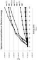
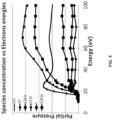
- a mass spectrometer may be used to study electron impact ionizations of several of the disclosed iodine-containing etching gases.
- the etch gases are allowed to flow through the mass spectrometer chamber and a Quadrupole mass spectrometer (Hiden Analytical Inc.) detector is used to study the fragments from the etch gas as a function of electron energy.
- the x-axis represents electron energy from 0-100 eV and y-axis represents the partial pressure in Torr of the fragment species.
- FIG. 4 is a graph demonstrating the electron impact ionization energy (eV) versus species concentration (Torr) of CF 3 I ( CAS No. 2314-97-8 ).
- the dominant fragments or ionized product produced at between 10 and 20 eV are CF 3 , I, and CF 3 I.
- FIG. 5 is a graph demonstrating the electron impact ionization energy (eV) versus species concentration (Torr) of C 2 F 3 I ( CAS No. 359-37-5 ).
- the dominant fragments produced at between 10 and 20 eV are CFI, CF, and I.
- FIG. 6 is a graph demonstrating the electron impact ionization energy (eV) versus species concentration (Torr) of C 2 F 5 I ( CAS No. 354-64-3 ).
- the dominant fragments or ionized product produced at between 10 and 20 eV are C 2 F 5 , C 2 F 5 I, CF 3 , and I.
- FIG. 7 is a graph demonstrating the electron impact ionization energy (eV) versus species concentration (Torr) of C 2 HF 4 I ( CAS No. 354-41-6 ).
- the dominant fragments produced at between 10 and 20 eV are C 2 HF 4 , CHF 2 , C 2 HF 3 , and I.
- FIG. 8 is a graph demonstrating the electron impact ionization energy (eV) versus species concentration (Torr) of C 3 F 5 I (CAS No. 431-65-2).
- the dominant fragments produced at between 10 and 20 eV are C 3 F 5 , CF 3 , and I.
- FIG. 9 is a graph demonstrating the electron impact ionization energy (eV) versus species concentration (Torr) of C 3 F 7 I ( CAS No. 754-34-7 ).
- the dominant fragments produced at between 10 and 20 eV are CF 3 , C 3 F 7 , and I.
- FIG. 10 is a graph demonstrating the electron impact ionization energy (eV) versus species concentration (Torr) of C 2 F 6 ( CAS No. 76-16-4 ).
- the dominant fragments produced at between 10 and 20 eV are CF 3 , C 3 F 7 , and I.
- FIG. 11 is a graph demonstrating the electron impact ionization energy (eV) versus species concentration (Torr) of C 3 F 8 ( CAS No. 76-19-7 ).
- the dominant CF 3 species of FIGS 10-11 is activated at a higher ionization energy when compared to the ionization energies needed to produce the dominant species of the analogous C2 and C3 compounds of FIGS 5-9 .
- etching experiments were performed on four 1 ⁇ 1 cm 2 coupons having four different substrate materials including SiO, SiN, p-Si, and a-C using a Lam 4520XLe 200 mm Dual CCP etcher.
- Deposition and/or etch rates are measured using an ellipsometer and/or scanning electron microscope (SEM) by measuring the change in etch thickness as a function of etching time.
- the coupons are placed on 200 mm diameter carrier wafer and held in contact by using double sided carbon tape obtained from 2spi manufacturer. Alternatively, thermal paste may have been used to stick coupons on carrier wafer.
- Deposition tests are performed on 1 ⁇ 1 cm 2 Si coupon at 30 mTorr, and source power of 750 W (27 MHz), with no bias power at the substrate.
- the process feed mixture contains 250 sccm of Ar and 15 sccm of etch gas.
- the deposition test sample is then sent for X-ray Photoelectron spectrometry (XPS) analysis to study the type of polymerizing film formed on the substrate.
- XPS X-ray Photoelectron spectrometry
- Etching tests are also performed at 30 mTorr, source power of 750 W (27 MHz), and bias power of 1500 W (2 MHz).
- the feed mixture contains 250 sccm of Ar, 15 sccm of etch gas, while O 2 is varied in the range 0 to 15 sccm.
- Fig. 12 is an exemplary cross-sectional side view of exemplary reactor system applied in deposition and etching tests.
- the reactor 800 includes a reactor chamber 802. Inside of the reactor chamber 802, a wafer 806 attached on the top of a bottom electrode 804 may be placed in the bottom portion of the reactor chamber 802 , and a silicon top electrode showerhead 808 may be placed on the top portion of the reactor chamber 802.
- the bottom electrode 804 may be an electrostatic chuck having bias power applied thereto. For example, 2 MHz RF bias power may be applied to the bottom electrode 804.
- the wafer 806 may have multiple layers that need to be etched.
- the silicon top electrode showerhead 808 has a plurality of holes 810 in the showerhead through which the gases pass.
- the gases may be introduced into the reactor chamber 802 through gas inlet 812 and then pass through holes 810 in the showerhead 808 for uniform gas distribution.
- Source power may be applied to the silicon top electrode showerhead 808.
- 27 MHz RF source power may be applied to the silicon top electrode showerhead 808.
- the gases passing through the holes 810 in the showerhead 808 may be ionized in the plasma region and then perform etching on the wafer 806.
- the gases may be removed by pumping the gases out of the reactor chamber 802 from outlet 814.
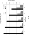
- FIG. 13 is a graph demonstrating etch rates of SiO, SiN, p-Si and a-C with CF 3 I and O 2 .
- the y-axis represents etch rates; the x-axis is O 2 flow rate in sccm; the CF 3 I flow rate is fixed at 15 sccm while the O 2 flow rate is varied from 0 to 20 sccm.
- FIG. 14 is a graph demonstrating etch rates of SiO, SiN, p-Si and a-C with C 2 F 3 I and O 2 .
- the positive y-axis represents etch rates while the negative y-axis represents deposition rates;
- the x-axis is O 2 flow rate in sccm;
- the C 2 F 3 I flow rate is fixed at 15 sccm while the O 2 flow rate is varied from 0 to 10 sccm.
- FIG. 15 is a graph demonstrating etch rates of SiO, SiN, p-Si and a-C with C 2 F 5 I and O 2 .
- the y-axis represents etch rates;
- the x-axis is O 2 flow rate in sccm;
- the C 2 F 5 I flow rate is fixed at 15 sccm while the O 2 flow rate is varied from 0 to 20 sccm.
- FIG. 16 is a graph demonstrating etch rates of SiO, SiN, p-Si and a-C with C 2 HF 4 I and O 2 .
- the positive y-axis represents etch rates while the negative y-axis represents deposition rates;
- the x-axis is O 2 flow rate in sccm;
- the C 2 HF 4 I flow rate is fixed at 15 sccm while the O 2 flow rate is varied from 0 to 15 sccm.
- FIG. 17 is a graph demonstrating etch rates of SiO, SiN, p-Si and a-C with C 3 F 5 I and O 2 .
- the positive y-axis represents etch rates while the negative y-axis represents deposition rates;
- the x-axis is O 2 flow rate in sccm;
- the C 3 F 5 I flow rate is fixed at 15 sccm while the O 2 flow rate is varied from 0 to 15 sccm.
- FIG. 18 is a graph demonstrating etch rates of SiO, SiN, p-Si and a-C with C 3 F 7 I and O 2 .
- the y-axis represents etch rates; the x-axis is O 2 flow rate in sccm; the C 3 F 7 I flow rate is fixed at 15 sccm while the O 2 flow rate is varied from 0 to 20 sccm.
- FIGS 14 , 16 , and 17 are from polymerizing gases having H or unsaturation and show deposition and infinite selectivity for etching oxide to a-C, polySi, and SiN. Whereas the saturated molecules of FIGS 13 , 15 , and 18 do not exhibit deposition and therefore do not have infinite selectivity, but still exhibit higher selectivity than non-Iodine containing etch gases.
- the evaluation of the dry etching of SiO, SiN, p-Si and a-C films with iodine-containing etching compounds shows that the iodine-containing HFCs yield highest (up to infinite) selectivity of silicon oxide to silicon nitride and p-Si than the prior art fluorocarbons.
- the reason for high selectivity may be attributed to the formation of low F/C iodine containing fragments during plasma dissociation of the etch gases, which results in the formation of a protective polymer film on the substrates.
- the iodine is ionized and bombards the surface with the heavy I ion similar to inert gases such as Ar, Kr, and Xe.
- the etching gas results presented herein show they are not only ready for contact etch process, but also may be beneficial for other etching processes on silicon or metal containing substrates, including low k etching processes.
Landscapes
- Engineering & Computer Science (AREA)
- Physics & Mathematics (AREA)
- Power Engineering (AREA)
- Computer Hardware Design (AREA)
- Microelectronics & Electronic Packaging (AREA)
- Condensed Matter Physics & Semiconductors (AREA)
- General Physics & Mathematics (AREA)
- Manufacturing & Machinery (AREA)
- Chemical & Material Sciences (AREA)
- Chemical Kinetics & Catalysis (AREA)
- General Chemical & Material Sciences (AREA)
- Plasma & Fusion (AREA)
- Inorganic Chemistry (AREA)
- Drying Of Semiconductors (AREA)
- Semiconductor Memories (AREA)
- Non-Volatile Memory (AREA)
- Insulated Gate Type Field-Effect Transistor (AREA)
Applications Claiming Priority (2)
| Application Number | Priority Date | Filing Date | Title |
|---|---|---|---|
| US15/396,220 US10607850B2 (en) | 2016-12-30 | 2016-12-30 | Iodine-containing compounds for etching semiconductor structures |
| PCT/US2017/069085 WO2018126206A1 (en) | 2016-12-30 | 2017-12-29 | Iodine-containing compounds for etching semiconductor structures |
Publications (3)
| Publication Number | Publication Date |
|---|---|
| EP3563406A1 EP3563406A1 (en) | 2019-11-06 |
| EP3563406A4 EP3563406A4 (en) | 2020-08-26 |
| EP3563406B1 true EP3563406B1 (en) | 2024-04-24 |
Family
ID=59066602
Family Applications (1)
| Application Number | Title | Priority Date | Filing Date |
|---|---|---|---|
| EP17889218.8A Active EP3563406B1 (en) | 2016-12-30 | 2017-12-29 | Iodine-containing compounds for etching semiconductor structures |
Country Status (7)
| Country | Link |
|---|---|
| US (2) | US10607850B2 (enExample) |
| EP (1) | EP3563406B1 (enExample) |
| JP (2) | JP7227135B2 (enExample) |
| KR (2) | KR102626466B1 (enExample) |
| CN (2) | CN110178206B (enExample) |
| TW (2) | TWI887536B (enExample) |
| WO (1) | WO2018126206A1 (enExample) |
Families Citing this family (37)
| Publication number | Priority date | Publication date | Assignee | Title |
|---|---|---|---|---|
| US20180277387A1 (en) * | 2014-08-06 | 2018-09-27 | American Air Liquide, Inc. | Gases for low damage selective silicon nitride etching |
| US10607850B2 (en) * | 2016-12-30 | 2020-03-31 | American Air Liquide, Inc. | Iodine-containing compounds for etching semiconductor structures |
| US10446681B2 (en) | 2017-07-10 | 2019-10-15 | Micron Technology, Inc. | NAND memory arrays, and devices comprising semiconductor channel material and nitrogen |
| US10276398B2 (en) * | 2017-08-02 | 2019-04-30 | Lam Research Corporation | High aspect ratio selective lateral etch using cyclic passivation and etching |
| DE102017128070B4 (de) * | 2017-08-31 | 2023-08-31 | Taiwan Semiconductor Manufacturing Company, Ltd. | Ätzen zum Verringern von Bahnunregelmässigkeiten |
| JP6883495B2 (ja) * | 2017-09-04 | 2021-06-09 | 東京エレクトロン株式会社 | エッチング方法 |
| JP2019050305A (ja) * | 2017-09-11 | 2019-03-28 | 東芝メモリ株式会社 | プラズマエッチング方法、及び、半導体装置の製造方法 |
| US10559466B2 (en) | 2017-12-27 | 2020-02-11 | Micron Technology, Inc. | Methods of forming a channel region of a transistor and methods used in forming a memory array |
| US10297611B1 (en) | 2017-12-27 | 2019-05-21 | Micron Technology, Inc. | Transistors and arrays of elevationally-extending strings of memory cells |
| US10529581B2 (en) * | 2017-12-29 | 2020-01-07 | L'Air Liquide, Société Anonyme pour l'Etude et l'Exploitation des Procédés Georges Claude | SiN selective etch to SiO2 with non-plasma dry process for 3D NAND device applications |
| JP7209567B2 (ja) * | 2018-07-30 | 2023-01-20 | 東京エレクトロン株式会社 | エッチング方法およびエッチング装置 |
| KR102272823B1 (ko) * | 2018-07-30 | 2021-07-02 | 도쿄엘렉트론가부시키가이샤 | 에칭 방법 및 에칭 장치 |
| EP3901991A4 (en) * | 2018-12-21 | 2022-08-17 | Showa Denko K.K. | ETCHING METHOD USING HALOGEN FLUORIDE AND SEMICONDUCTOR PRODUCTION METHOD |
| US11145504B2 (en) * | 2019-01-14 | 2021-10-12 | Applied Materials, Inc. | Method of forming film stacks with reduced defects |
| CN113330539A (zh) * | 2019-01-23 | 2021-08-31 | 中央硝子株式会社 | 干蚀刻方法、干蚀刻剂及其保存容器 |
| US10629451B1 (en) * | 2019-02-01 | 2020-04-21 | American Air Liquide, Inc. | Method to improve profile control during selective etching of silicon nitride spacers |
| US10978473B2 (en) * | 2019-02-12 | 2021-04-13 | Taiwan Semiconductor Manufacturing Co., Ltd. | Flash memory structure and method of forming the same |
| SG11202109169TA (en) * | 2019-03-22 | 2021-09-29 | Central Glass Co Ltd | Dry etching method and method for producing semiconductor device |
| JP7604145B2 (ja) * | 2019-11-25 | 2024-12-23 | 東京エレクトロン株式会社 | 基板処理方法及びプラズマ処理装置 |
| US11521846B2 (en) * | 2019-12-16 | 2022-12-06 | Taiwan Semiconductor Manufacturing Company Limited | Methods for patterning a silicon oxide-silicon nitride-silicon oxide stack and structures formed by the same |
| KR102664702B1 (ko) * | 2020-02-14 | 2024-05-09 | 한양대학교 산학협력단 | 식각 선택비의 조절에 의한 미세패턴의 형성방법 |
| FR3107280B1 (fr) * | 2020-02-19 | 2023-01-13 | Arkema France | Composition comprenant un composé iodofluorocarbure |
| JP2021163839A (ja) * | 2020-03-31 | 2021-10-11 | 東京エレクトロン株式会社 | エッチング方法及びプラズマ処理装置 |
| US11798811B2 (en) * | 2020-06-26 | 2023-10-24 | American Air Liquide, Inc. | Iodine-containing fluorocarbon and hydrofluorocarbon compounds for etching semiconductor structures |
| CN116325087A (zh) * | 2020-10-15 | 2023-06-23 | 株式会社力森诺科 | 蚀刻气体、蚀刻方法和半导体元件的制造方法 |
| US12106971B2 (en) * | 2020-12-28 | 2024-10-01 | American Air Liquide, Inc. | High conductive passivation layers and method of forming the same during high aspect ratio plasma etching |
| US11538919B2 (en) | 2021-02-23 | 2022-12-27 | Micron Technology, Inc. | Transistors and arrays of elevationally-extending strings of memory cells |
| KR20220122260A (ko) * | 2021-02-26 | 2022-09-02 | 에스케이스페셜티 주식회사 | 실리콘 함유막의 다중 적층체의 식각 방법 및 이를 포함하는 반도체 디바이스의 제조방법 |
| KR20220126045A (ko) * | 2021-03-08 | 2022-09-15 | 에스케이스페셜티 주식회사 | 실리콘 함유막의 다중 적층체의 식각 방법 및 이를 포함하는 반도체 디바이스의 제조방법 |
| US20220293430A1 (en) * | 2021-03-12 | 2022-09-15 | Applied Materials, Inc. | Isotropic silicon nitride removal |
| JP7638119B2 (ja) * | 2021-03-15 | 2025-03-03 | 株式会社Screenホールディングス | 基板処理方法および基板処理装置 |
| CN114023879B (zh) * | 2021-10-20 | 2025-02-11 | 上海华虹宏力半导体制造有限公司 | 表面粗糙的多晶硅结构的刻蚀方法 |
| US12188123B2 (en) | 2021-12-17 | 2025-01-07 | American Air Liquide, Inc. | Deposition of iodine-containing carbon films |
| US12272562B2 (en) * | 2021-12-17 | 2025-04-08 | L'Aire Liquide, Société Anonyme pour l'Etude et l'Exploitation des Procédés Georges Claude | Oxygen and iodine-containing hydrofluorocarbon compound for etching semiconductor structures |
| WO2024064526A1 (en) * | 2022-09-13 | 2024-03-28 | Lam Research Corporation | Method for etching features in a stack |
| WO2024059467A1 (en) * | 2022-09-13 | 2024-03-21 | Lam Research Corporation | Method for etching features using hf gas |
| WO2025117301A1 (en) * | 2023-11-27 | 2025-06-05 | Lam Research Corporation | SELECTIVE ETCH OF STACK USING A HYDROGEN CONTAINING COMPONENT AND AT LEAST ONE OF SeF6, AND IF7 AND TeF6 |
Family Cites Families (36)
| Publication number | Priority date | Publication date | Assignee | Title |
|---|---|---|---|---|
| JP3371143B2 (ja) * | 1991-06-03 | 2003-01-27 | ソニー株式会社 | ドライエッチング方法 |
| EP0854502A3 (en) * | 1997-01-21 | 1998-09-02 | Texas Instruments Incorporated | Iodofluorocarbon gas for the etching of dielectric layers and the cleaning of process chambers |
| JPH10223614A (ja) | 1997-02-12 | 1998-08-21 | Daikin Ind Ltd | エッチングガスおよびクリーニングガス |
| JP3559691B2 (ja) * | 1997-09-04 | 2004-09-02 | 株式会社日立製作所 | 半導体装置の製造方法 |
| US6387287B1 (en) | 1998-03-27 | 2002-05-14 | Applied Materials, Inc. | Process for etching oxide using a hexafluorobutadiene and manifesting a wide process window |
| JP3570903B2 (ja) | 1998-09-25 | 2004-09-29 | 株式会社ルネサステクノロジ | 半導体装置の製造方法 |
| US7931820B2 (en) * | 2000-09-07 | 2011-04-26 | Daikin Industries, Ltd. | Dry etching gas and method for dry etching |
| WO2002039494A1 (en) | 2000-11-08 | 2002-05-16 | Daikin Industries, Ltd. | Dry etching gas and method for dry etching |
| JP2002319574A (ja) * | 2001-04-23 | 2002-10-31 | Nec Corp | 窒化シリコン膜の除去方法 |
| US6921725B2 (en) * | 2001-06-28 | 2005-07-26 | Micron Technology, Inc. | Etching of high aspect ratio structures |
| US7547635B2 (en) * | 2002-06-14 | 2009-06-16 | Lam Research Corporation | Process for etching dielectric films with improved resist and/or etch profile characteristics |
| CN100342952C (zh) * | 2003-01-29 | 2007-10-17 | 昭和电工株式会社 | 分解氟化合物的方法 |
| US20050241671A1 (en) * | 2004-04-29 | 2005-11-03 | Dong Chun C | Method for removing a substance from a substrate using electron attachment |
| JP4761502B2 (ja) | 2004-10-07 | 2011-08-31 | 株式会社アルバック | 層間絶縁膜のドライエッチング方法 |
| US20090191715A1 (en) * | 2006-03-09 | 2009-07-30 | Toshio Hayashi | Method for etching interlayer dielectric film |
| TW200735206A (en) | 2006-03-10 | 2007-09-16 | Philtech Inc | Method of dry etching of interlayer insulation film and etching device |
| US8125069B2 (en) * | 2006-04-07 | 2012-02-28 | Philtech Inc. | Semiconductor device and etching apparatus |
| US7517804B2 (en) | 2006-08-31 | 2009-04-14 | Micron Technologies, Inc. | Selective etch chemistries for forming high aspect ratio features and associated structures |
| US20080191163A1 (en) | 2007-02-09 | 2008-08-14 | Mocella Michael T | Laser-Assisted Etching Using Gas Compositions Comprising Unsaturated Fluorocarbons |
| US8614151B2 (en) * | 2008-01-04 | 2013-12-24 | Micron Technology, Inc. | Method of etching a high aspect ratio contact |
| JP4982443B2 (ja) * | 2008-07-14 | 2012-07-25 | 株式会社アルバック | 層間絶縁膜のドライエッチング方法 |
| US8372756B2 (en) * | 2008-08-29 | 2013-02-12 | Air Products And Chemicals, Inc. | Selective etching of silicon dioxide compositions |
| WO2011031858A1 (en) * | 2009-09-10 | 2011-03-17 | Matheson Tri-Gas, Inc. | High aspect ratio silicon oxide etch |
| JP2011071223A (ja) * | 2009-09-24 | 2011-04-07 | Ulvac Japan Ltd | ドライエッチング方法 |
| KR101660488B1 (ko) | 2010-01-22 | 2016-09-28 | 삼성전자주식회사 | 3차원 반도체 장치 및 그 제조 방법 |
| JP5850043B2 (ja) | 2011-03-17 | 2016-02-03 | 日本ゼオン株式会社 | エッチングガスおよびエッチング方法 |
| US8603921B2 (en) * | 2011-07-25 | 2013-12-10 | Applied Materials, Inc. | Maintaining mask integrity to form openings in wafers |
| US8512586B2 (en) * | 2011-09-01 | 2013-08-20 | Tel Epion Inc. | Gas cluster ion beam etching process for achieving target etch process metrics for multiple materials |
| US20150270135A1 (en) * | 2011-09-01 | 2015-09-24 | Tel Epion Inc. | Gas cluster ion beam etching process |
| CN107275206B (zh) * | 2012-10-30 | 2021-03-26 | 乔治洛德方法研究和开发液化空气有限公司 | 用于高纵横比氧化物蚀刻的氟碳分子 |
| TWI612182B (zh) * | 2013-09-09 | 2018-01-21 | 液態空氣喬治斯克勞帝方法研究開發股份有限公司 | 用蝕刻氣體蝕刻半導體結構的方法 |
| KR102333443B1 (ko) | 2014-10-24 | 2021-12-02 | 삼성전자주식회사 | 반도체 소자의 제조 방법 |
| US9728422B2 (en) | 2015-01-23 | 2017-08-08 | Central Glass Company, Limited | Dry etching method |
| JP6544215B2 (ja) * | 2015-01-23 | 2019-07-17 | セントラル硝子株式会社 | ドライエッチング方法 |
| US9659788B2 (en) * | 2015-08-31 | 2017-05-23 | American Air Liquide, Inc. | Nitrogen-containing compounds for etching semiconductor structures |
| US10607850B2 (en) | 2016-12-30 | 2020-03-31 | American Air Liquide, Inc. | Iodine-containing compounds for etching semiconductor structures |
-
2016
- 2016-12-30 US US15/396,220 patent/US10607850B2/en active Active
-
2017
- 2017-12-21 TW TW111112039A patent/TWI887536B/zh active
- 2017-12-21 TW TW106145082A patent/TWI756330B/zh active
- 2017-12-29 CN CN201780081811.0A patent/CN110178206B/zh active Active
- 2017-12-29 JP JP2019536103A patent/JP7227135B2/ja active Active
- 2017-12-29 WO PCT/US2017/069085 patent/WO2018126206A1/en not_active Ceased
- 2017-12-29 CN CN202311017020.5A patent/CN116884838A/zh active Pending
- 2017-12-29 EP EP17889218.8A patent/EP3563406B1/en active Active
- 2017-12-29 KR KR1020237016440A patent/KR102626466B1/ko active Active
- 2017-12-29 KR KR1020197020788A patent/KR102537653B1/ko active Active
-
2020
- 2020-03-03 US US16/807,247 patent/US11430663B2/en active Active
-
2023
- 2023-02-09 JP JP2023018581A patent/JP7470834B2/ja active Active
Also Published As
| Publication number | Publication date |
|---|---|
| TW202229216A (zh) | 2022-08-01 |
| JP2020515047A (ja) | 2020-05-21 |
| TW201825446A (zh) | 2018-07-16 |
| JP2023053121A (ja) | 2023-04-12 |
| KR102537653B1 (ko) | 2023-05-26 |
| US10607850B2 (en) | 2020-03-31 |
| TWI756330B (zh) | 2022-03-01 |
| EP3563406A1 (en) | 2019-11-06 |
| CN110178206B (zh) | 2023-08-18 |
| TWI887536B (zh) | 2025-06-21 |
| US11430663B2 (en) | 2022-08-30 |
| KR20230070539A (ko) | 2023-05-23 |
| CN116884838A (zh) | 2023-10-13 |
| EP3563406A4 (en) | 2020-08-26 |
| JP7470834B2 (ja) | 2024-04-18 |
| WO2018126206A1 (en) | 2018-07-05 |
| US20200203174A1 (en) | 2020-06-25 |
| US20170178923A1 (en) | 2017-06-22 |
| CN110178206A (zh) | 2019-08-27 |
| KR20190093221A (ko) | 2019-08-08 |
| JP7227135B2 (ja) | 2023-02-21 |
| KR102626466B1 (ko) | 2024-01-17 |
Similar Documents
| Publication | Publication Date | Title |
|---|---|---|
| EP3563406B1 (en) | Iodine-containing compounds for etching semiconductor structures | |
| US11152223B2 (en) | Fluorocarbon molecules for high aspect ratio oxide etch | |
| US10256109B2 (en) | Nitrogen-containing compounds for etching semiconductor structures | |
| JP7775553B2 (ja) | 半導体構造エッチング用ヨウ素含有フルオロカーボン及びハイドロフルオロカーボン化合物 | |
| TWI846218B (zh) | 用於蝕刻半導體結構的含氧和碘的氫氟烴化合物 |
Legal Events
| Date | Code | Title | Description |
|---|---|---|---|
| STAA | Information on the status of an ep patent application or granted ep patent |
Free format text: STATUS: THE INTERNATIONAL PUBLICATION HAS BEEN MADE |
|
| PUAI | Public reference made under article 153(3) epc to a published international application that has entered the european phase |
Free format text: ORIGINAL CODE: 0009012 |
|
| STAA | Information on the status of an ep patent application or granted ep patent |
Free format text: STATUS: REQUEST FOR EXAMINATION WAS MADE |
|
| 17P | Request for examination filed |
Effective date: 20190730 |
|
| AK | Designated contracting states |
Kind code of ref document: A1 Designated state(s): AL AT BE BG CH CY CZ DE DK EE ES FI FR GB GR HR HU IE IS IT LI LT LU LV MC MK MT NL NO PL PT RO RS SE SI SK SM TR |
|
| AX | Request for extension of the european patent |
Extension state: BA ME |
|
| DAV | Request for validation of the european patent (deleted) | ||
| DAX | Request for extension of the european patent (deleted) | ||
| A4 | Supplementary search report drawn up and despatched |
Effective date: 20200728 |
|
| RIC1 | Information provided on ipc code assigned before grant |
Ipc: H01L 27/115 20170101ALN20200722BHEP Ipc: H01L 21/308 20060101ALI20200722BHEP Ipc: H01L 21/311 20060101AFI20200722BHEP |
|
| RAP3 | Party data changed (applicant data changed or rights of an application transferred) |
Owner name: L'AIR LIQUIDE, SOCIETE ANONYME POUR L'ETUDE ET L'EXPLOITATION DES PROCEDES GEORGES CLAUDE |
|
| GRAP | Despatch of communication of intention to grant a patent |
Free format text: ORIGINAL CODE: EPIDOSNIGR1 |
|
| STAA | Information on the status of an ep patent application or granted ep patent |
Free format text: STATUS: GRANT OF PATENT IS INTENDED |
|
| RIC1 | Information provided on ipc code assigned before grant |
Ipc: H10B 43/27 20230101ALI20230630BHEP Ipc: H01L 21/3213 20060101ALI20230630BHEP Ipc: H01L 21/311 20060101AFI20230630BHEP |
|
| INTG | Intention to grant announced |
Effective date: 20230731 |
|
| GRAJ | Information related to disapproval of communication of intention to grant by the applicant or resumption of examination proceedings by the epo deleted |
Free format text: ORIGINAL CODE: EPIDOSDIGR1 |
|
| STAA | Information on the status of an ep patent application or granted ep patent |
Free format text: STATUS: REQUEST FOR EXAMINATION WAS MADE |
|
| INTC | Intention to grant announced (deleted) | ||
| GRAP | Despatch of communication of intention to grant a patent |
Free format text: ORIGINAL CODE: EPIDOSNIGR1 |
|
| STAA | Information on the status of an ep patent application or granted ep patent |
Free format text: STATUS: GRANT OF PATENT IS INTENDED |
|
| INTG | Intention to grant announced |
Effective date: 20240112 |
|
| GRAS | Grant fee paid |
Free format text: ORIGINAL CODE: EPIDOSNIGR3 |
|
| GRAA | (expected) grant |
Free format text: ORIGINAL CODE: 0009210 |
|
| STAA | Information on the status of an ep patent application or granted ep patent |
Free format text: STATUS: THE PATENT HAS BEEN GRANTED |
|
| AK | Designated contracting states |
Kind code of ref document: B1 Designated state(s): AL AT BE BG CH CY CZ DE DK EE ES FI FR GB GR HR HU IE IS IT LI LT LU LV MC MK MT NL NO PL PT RO RS SE SI SK SM TR |
|
| REG | Reference to a national code |
Ref country code: GB Ref legal event code: FG4D |
|
| REG | Reference to a national code |
Ref country code: CH Ref legal event code: EP |
|
| REG | Reference to a national code |
Ref country code: DE Ref legal event code: R096 Ref document number: 602017081404 Country of ref document: DE |
|
| REG | Reference to a national code |
Ref country code: IE Ref legal event code: FG4D |
|
| REG | Reference to a national code |
Ref country code: LT Ref legal event code: MG9D |
|
| REG | Reference to a national code |
Ref country code: NL Ref legal event code: MP Effective date: 20240424 |
|
| REG | Reference to a national code |
Ref country code: AT Ref legal event code: MK05 Ref document number: 1680573 Country of ref document: AT Kind code of ref document: T Effective date: 20240424 |
|
| PG25 | Lapsed in a contracting state [announced via postgrant information from national office to epo] |
Ref country code: NL Free format text: LAPSE BECAUSE OF FAILURE TO SUBMIT A TRANSLATION OF THE DESCRIPTION OR TO PAY THE FEE WITHIN THE PRESCRIBED TIME-LIMIT Effective date: 20240424 |
|
| PG25 | Lapsed in a contracting state [announced via postgrant information from national office to epo] |
Ref country code: NL Free format text: LAPSE BECAUSE OF FAILURE TO SUBMIT A TRANSLATION OF THE DESCRIPTION OR TO PAY THE FEE WITHIN THE PRESCRIBED TIME-LIMIT Effective date: 20240424 |
|
| PG25 | Lapsed in a contracting state [announced via postgrant information from national office to epo] |
Ref country code: IS Free format text: LAPSE BECAUSE OF FAILURE TO SUBMIT A TRANSLATION OF THE DESCRIPTION OR TO PAY THE FEE WITHIN THE PRESCRIBED TIME-LIMIT Effective date: 20240824 |
|
| PG25 | Lapsed in a contracting state [announced via postgrant information from national office to epo] |
Ref country code: BG Free format text: LAPSE BECAUSE OF FAILURE TO SUBMIT A TRANSLATION OF THE DESCRIPTION OR TO PAY THE FEE WITHIN THE PRESCRIBED TIME-LIMIT Effective date: 20240424 |
|
| PG25 | Lapsed in a contracting state [announced via postgrant information from national office to epo] |
Ref country code: HR Free format text: LAPSE BECAUSE OF FAILURE TO SUBMIT A TRANSLATION OF THE DESCRIPTION OR TO PAY THE FEE WITHIN THE PRESCRIBED TIME-LIMIT Effective date: 20240424 Ref country code: FI Free format text: LAPSE BECAUSE OF FAILURE TO SUBMIT A TRANSLATION OF THE DESCRIPTION OR TO PAY THE FEE WITHIN THE PRESCRIBED TIME-LIMIT Effective date: 20240424 |
|
| PG25 | Lapsed in a contracting state [announced via postgrant information from national office to epo] |
Ref country code: GR Free format text: LAPSE BECAUSE OF FAILURE TO SUBMIT A TRANSLATION OF THE DESCRIPTION OR TO PAY THE FEE WITHIN THE PRESCRIBED TIME-LIMIT Effective date: 20240725 |
|
| PG25 | Lapsed in a contracting state [announced via postgrant information from national office to epo] |
Ref country code: PT Free format text: LAPSE BECAUSE OF FAILURE TO SUBMIT A TRANSLATION OF THE DESCRIPTION OR TO PAY THE FEE WITHIN THE PRESCRIBED TIME-LIMIT Effective date: 20240826 |
|
| PG25 | Lapsed in a contracting state [announced via postgrant information from national office to epo] |
Ref country code: ES Free format text: LAPSE BECAUSE OF FAILURE TO SUBMIT A TRANSLATION OF THE DESCRIPTION OR TO PAY THE FEE WITHIN THE PRESCRIBED TIME-LIMIT Effective date: 20240424 |
|
| PG25 | Lapsed in a contracting state [announced via postgrant information from national office to epo] |
Ref country code: AT Free format text: LAPSE BECAUSE OF FAILURE TO SUBMIT A TRANSLATION OF THE DESCRIPTION OR TO PAY THE FEE WITHIN THE PRESCRIBED TIME-LIMIT Effective date: 20240424 |
|
| PG25 | Lapsed in a contracting state [announced via postgrant information from national office to epo] |
Ref country code: PL Free format text: LAPSE BECAUSE OF FAILURE TO SUBMIT A TRANSLATION OF THE DESCRIPTION OR TO PAY THE FEE WITHIN THE PRESCRIBED TIME-LIMIT Effective date: 20240424 |
|
| PG25 | Lapsed in a contracting state [announced via postgrant information from national office to epo] |
Ref country code: LV Free format text: LAPSE BECAUSE OF FAILURE TO SUBMIT A TRANSLATION OF THE DESCRIPTION OR TO PAY THE FEE WITHIN THE PRESCRIBED TIME-LIMIT Effective date: 20240424 |
|
| PG25 | Lapsed in a contracting state [announced via postgrant information from national office to epo] |
Ref country code: PT Free format text: LAPSE BECAUSE OF FAILURE TO SUBMIT A TRANSLATION OF THE DESCRIPTION OR TO PAY THE FEE WITHIN THE PRESCRIBED TIME-LIMIT Effective date: 20240826 Ref country code: PL Free format text: LAPSE BECAUSE OF FAILURE TO SUBMIT A TRANSLATION OF THE DESCRIPTION OR TO PAY THE FEE WITHIN THE PRESCRIBED TIME-LIMIT Effective date: 20240424 Ref country code: NO Free format text: LAPSE BECAUSE OF FAILURE TO SUBMIT A TRANSLATION OF THE DESCRIPTION OR TO PAY THE FEE WITHIN THE PRESCRIBED TIME-LIMIT Effective date: 20240724 Ref country code: LV Free format text: LAPSE BECAUSE OF FAILURE TO SUBMIT A TRANSLATION OF THE DESCRIPTION OR TO PAY THE FEE WITHIN THE PRESCRIBED TIME-LIMIT Effective date: 20240424 Ref country code: IS Free format text: LAPSE BECAUSE OF FAILURE TO SUBMIT A TRANSLATION OF THE DESCRIPTION OR TO PAY THE FEE WITHIN THE PRESCRIBED TIME-LIMIT Effective date: 20240824 Ref country code: HR Free format text: LAPSE BECAUSE OF FAILURE TO SUBMIT A TRANSLATION OF THE DESCRIPTION OR TO PAY THE FEE WITHIN THE PRESCRIBED TIME-LIMIT Effective date: 20240424 Ref country code: GR Free format text: LAPSE BECAUSE OF FAILURE TO SUBMIT A TRANSLATION OF THE DESCRIPTION OR TO PAY THE FEE WITHIN THE PRESCRIBED TIME-LIMIT Effective date: 20240725 Ref country code: FI Free format text: LAPSE BECAUSE OF FAILURE TO SUBMIT A TRANSLATION OF THE DESCRIPTION OR TO PAY THE FEE WITHIN THE PRESCRIBED TIME-LIMIT Effective date: 20240424 Ref country code: ES Free format text: LAPSE BECAUSE OF FAILURE TO SUBMIT A TRANSLATION OF THE DESCRIPTION OR TO PAY THE FEE WITHIN THE PRESCRIBED TIME-LIMIT Effective date: 20240424 Ref country code: BG Free format text: LAPSE BECAUSE OF FAILURE TO SUBMIT A TRANSLATION OF THE DESCRIPTION OR TO PAY THE FEE WITHIN THE PRESCRIBED TIME-LIMIT Effective date: 20240424 Ref country code: AT Free format text: LAPSE BECAUSE OF FAILURE TO SUBMIT A TRANSLATION OF THE DESCRIPTION OR TO PAY THE FEE WITHIN THE PRESCRIBED TIME-LIMIT Effective date: 20240424 Ref country code: RS Free format text: LAPSE BECAUSE OF FAILURE TO SUBMIT A TRANSLATION OF THE DESCRIPTION OR TO PAY THE FEE WITHIN THE PRESCRIBED TIME-LIMIT Effective date: 20240724 |
|
| PGFP | Annual fee paid to national office [announced via postgrant information from national office to epo] |
Ref country code: DE Payment date: 20241210 Year of fee payment: 8 |
|
| PG25 | Lapsed in a contracting state [announced via postgrant information from national office to epo] |
Ref country code: DK Free format text: LAPSE BECAUSE OF FAILURE TO SUBMIT A TRANSLATION OF THE DESCRIPTION OR TO PAY THE FEE WITHIN THE PRESCRIBED TIME-LIMIT Effective date: 20240424 |
|
| PGFP | Annual fee paid to national office [announced via postgrant information from national office to epo] |
Ref country code: BE Payment date: 20241219 Year of fee payment: 8 |
|
| PGFP | Annual fee paid to national office [announced via postgrant information from national office to epo] |
Ref country code: FR Payment date: 20241224 Year of fee payment: 8 |
|
| PG25 | Lapsed in a contracting state [announced via postgrant information from national office to epo] |
Ref country code: EE Free format text: LAPSE BECAUSE OF FAILURE TO SUBMIT A TRANSLATION OF THE DESCRIPTION OR TO PAY THE FEE WITHIN THE PRESCRIBED TIME-LIMIT Effective date: 20240424 |
|
| PG25 | Lapsed in a contracting state [announced via postgrant information from national office to epo] |
Ref country code: CZ Free format text: LAPSE BECAUSE OF FAILURE TO SUBMIT A TRANSLATION OF THE DESCRIPTION OR TO PAY THE FEE WITHIN THE PRESCRIBED TIME-LIMIT Effective date: 20240424 |
|
| PG25 | Lapsed in a contracting state [announced via postgrant information from national office to epo] |
Ref country code: RO Free format text: LAPSE BECAUSE OF FAILURE TO SUBMIT A TRANSLATION OF THE DESCRIPTION OR TO PAY THE FEE WITHIN THE PRESCRIBED TIME-LIMIT Effective date: 20240424 Ref country code: SK Free format text: LAPSE BECAUSE OF FAILURE TO SUBMIT A TRANSLATION OF THE DESCRIPTION OR TO PAY THE FEE WITHIN THE PRESCRIBED TIME-LIMIT Effective date: 20240424 |
|
| REG | Reference to a national code |
Ref country code: DE Ref legal event code: R097 Ref document number: 602017081404 Country of ref document: DE |
|
| PG25 | Lapsed in a contracting state [announced via postgrant information from national office to epo] |
Ref country code: SM Free format text: LAPSE BECAUSE OF FAILURE TO SUBMIT A TRANSLATION OF THE DESCRIPTION OR TO PAY THE FEE WITHIN THE PRESCRIBED TIME-LIMIT Effective date: 20240424 |
|
| PG25 | Lapsed in a contracting state [announced via postgrant information from national office to epo] |
Ref country code: SM Free format text: LAPSE BECAUSE OF FAILURE TO SUBMIT A TRANSLATION OF THE DESCRIPTION OR TO PAY THE FEE WITHIN THE PRESCRIBED TIME-LIMIT Effective date: 20240424 Ref country code: SK Free format text: LAPSE BECAUSE OF FAILURE TO SUBMIT A TRANSLATION OF THE DESCRIPTION OR TO PAY THE FEE WITHIN THE PRESCRIBED TIME-LIMIT Effective date: 20240424 Ref country code: RO Free format text: LAPSE BECAUSE OF FAILURE TO SUBMIT A TRANSLATION OF THE DESCRIPTION OR TO PAY THE FEE WITHIN THE PRESCRIBED TIME-LIMIT Effective date: 20240424 Ref country code: EE Free format text: LAPSE BECAUSE OF FAILURE TO SUBMIT A TRANSLATION OF THE DESCRIPTION OR TO PAY THE FEE WITHIN THE PRESCRIBED TIME-LIMIT Effective date: 20240424 Ref country code: DK Free format text: LAPSE BECAUSE OF FAILURE TO SUBMIT A TRANSLATION OF THE DESCRIPTION OR TO PAY THE FEE WITHIN THE PRESCRIBED TIME-LIMIT Effective date: 20240424 Ref country code: CZ Free format text: LAPSE BECAUSE OF FAILURE TO SUBMIT A TRANSLATION OF THE DESCRIPTION OR TO PAY THE FEE WITHIN THE PRESCRIBED TIME-LIMIT Effective date: 20240424 |
|
| PLBE | No opposition filed within time limit |
Free format text: ORIGINAL CODE: 0009261 |
|
| STAA | Information on the status of an ep patent application or granted ep patent |
Free format text: STATUS: NO OPPOSITION FILED WITHIN TIME LIMIT |
|
| 26N | No opposition filed |
Effective date: 20250127 |
|
| PG25 | Lapsed in a contracting state [announced via postgrant information from national office to epo] |
Ref country code: SI Free format text: LAPSE BECAUSE OF FAILURE TO SUBMIT A TRANSLATION OF THE DESCRIPTION OR TO PAY THE FEE WITHIN THE PRESCRIBED TIME-LIMIT Effective date: 20240424 |
|
| PG25 | Lapsed in a contracting state [announced via postgrant information from national office to epo] |
Ref country code: MC Free format text: LAPSE BECAUSE OF FAILURE TO SUBMIT A TRANSLATION OF THE DESCRIPTION OR TO PAY THE FEE WITHIN THE PRESCRIBED TIME-LIMIT Effective date: 20240424 |
|
| REG | Reference to a national code |
Ref country code: CH Ref legal event code: PL |
|
| PG25 | Lapsed in a contracting state [announced via postgrant information from national office to epo] |
Ref country code: LU Free format text: LAPSE BECAUSE OF NON-PAYMENT OF DUE FEES Effective date: 20241229 |
|
| GBPC | Gb: european patent ceased through non-payment of renewal fee |
Effective date: 20241229 |
|
| PG25 | Lapsed in a contracting state [announced via postgrant information from national office to epo] |
Ref country code: SE Free format text: LAPSE BECAUSE OF FAILURE TO SUBMIT A TRANSLATION OF THE DESCRIPTION OR TO PAY THE FEE WITHIN THE PRESCRIBED TIME-LIMIT Effective date: 20240424 |
|
| PG25 | Lapsed in a contracting state [announced via postgrant information from national office to epo] |
Ref country code: GB Free format text: LAPSE BECAUSE OF NON-PAYMENT OF DUE FEES Effective date: 20241229 |
|
| PG25 | Lapsed in a contracting state [announced via postgrant information from national office to epo] |
Ref country code: CH Free format text: LAPSE BECAUSE OF NON-PAYMENT OF DUE FEES Effective date: 20241231 |
|
| PG25 | Lapsed in a contracting state [announced via postgrant information from national office to epo] |
Ref country code: IE Free format text: LAPSE BECAUSE OF NON-PAYMENT OF DUE FEES Effective date: 20241229 |