EP3553810A2 - Dispositif à semiconducteurs et son procédé de fabrication utilisant un masque espaceur - Google Patents
Dispositif à semiconducteurs et son procédé de fabrication utilisant un masque espaceur Download PDFInfo
- Publication number
- EP3553810A2 EP3553810A2 EP19160999.9A EP19160999A EP3553810A2 EP 3553810 A2 EP3553810 A2 EP 3553810A2 EP 19160999 A EP19160999 A EP 19160999A EP 3553810 A2 EP3553810 A2 EP 3553810A2
- Authority
- EP
- European Patent Office
- Prior art keywords
- layer
- opening
- mask layer
- mask
- spacer
- Prior art date
- Legal status (The legal status is an assumption and is not a legal conclusion. Google has not performed a legal analysis and makes no representation as to the accuracy of the status listed.)
- Granted
Links
Images
















Classifications
-
- H—ELECTRICITY
- H10—SEMICONDUCTOR DEVICES; ELECTRIC SOLID-STATE DEVICES NOT OTHERWISE PROVIDED FOR
- H10P—GENERIC PROCESSES OR APPARATUS FOR THE MANUFACTURE OR TREATMENT OF DEVICES COVERED BY CLASS H10
- H10P76/00—Manufacture or treatment of masks on semiconductor bodies, e.g. by lithography or photolithography
- H10P76/20—Manufacture or treatment of masks on semiconductor bodies, e.g. by lithography or photolithography of masks comprising organic materials
- H10P76/204—Manufacture or treatment of masks on semiconductor bodies, e.g. by lithography or photolithography of masks comprising organic materials of organic photoresist masks
- H10P76/2041—Photolithographic processes
-
- H—ELECTRICITY
- H10—SEMICONDUCTOR DEVICES; ELECTRIC SOLID-STATE DEVICES NOT OTHERWISE PROVIDED FOR
- H10P—GENERIC PROCESSES OR APPARATUS FOR THE MANUFACTURE OR TREATMENT OF DEVICES COVERED BY CLASS H10
- H10P76/00—Manufacture or treatment of masks on semiconductor bodies, e.g. by lithography or photolithography
- H10P76/40—Manufacture or treatment of masks on semiconductor bodies, e.g. by lithography or photolithography of masks comprising inorganic materials
- H10P76/408—Manufacture or treatment of masks on semiconductor bodies, e.g. by lithography or photolithography of masks comprising inorganic materials characterised by their sizes, orientations, dispositions, behaviours or shapes
- H10P76/4085—Manufacture or treatment of masks on semiconductor bodies, e.g. by lithography or photolithography of masks comprising inorganic materials characterised by their sizes, orientations, dispositions, behaviours or shapes characterised by the processes involved to create the masks
-
- H—ELECTRICITY
- H10—SEMICONDUCTOR DEVICES; ELECTRIC SOLID-STATE DEVICES NOT OTHERWISE PROVIDED FOR
- H10P—GENERIC PROCESSES OR APPARATUS FOR THE MANUFACTURE OR TREATMENT OF DEVICES COVERED BY CLASS H10
- H10P50/00—Etching of wafers, substrates or parts of devices
- H10P50/20—Dry etching; Plasma etching; Reactive-ion etching
- H10P50/28—Dry etching; Plasma etching; Reactive-ion etching of insulating materials
-
- H—ELECTRICITY
- H10—SEMICONDUCTOR DEVICES; ELECTRIC SOLID-STATE DEVICES NOT OTHERWISE PROVIDED FOR
- H10P—GENERIC PROCESSES OR APPARATUS FOR THE MANUFACTURE OR TREATMENT OF DEVICES COVERED BY CLASS H10
- H10P50/00—Etching of wafers, substrates or parts of devices
- H10P50/71—Etching of wafers, substrates or parts of devices using masks for conductive or resistive materials
-
- H—ELECTRICITY
- H10—SEMICONDUCTOR DEVICES; ELECTRIC SOLID-STATE DEVICES NOT OTHERWISE PROVIDED FOR
- H10P—GENERIC PROCESSES OR APPARATUS FOR THE MANUFACTURE OR TREATMENT OF DEVICES COVERED BY CLASS H10
- H10P50/00—Etching of wafers, substrates or parts of devices
- H10P50/73—Etching of wafers, substrates or parts of devices using masks for insulating materials
-
- H—ELECTRICITY
- H10—SEMICONDUCTOR DEVICES; ELECTRIC SOLID-STATE DEVICES NOT OTHERWISE PROVIDED FOR
- H10P—GENERIC PROCESSES OR APPARATUS FOR THE MANUFACTURE OR TREATMENT OF DEVICES COVERED BY CLASS H10
- H10P76/00—Manufacture or treatment of masks on semiconductor bodies, e.g. by lithography or photolithography
- H10P76/40—Manufacture or treatment of masks on semiconductor bodies, e.g. by lithography or photolithography of masks comprising inorganic materials
- H10P76/405—Manufacture or treatment of masks on semiconductor bodies, e.g. by lithography or photolithography of masks comprising inorganic materials characterised by their composition, e.g. multilayer masks
-
- H—ELECTRICITY
- H10—SEMICONDUCTOR DEVICES; ELECTRIC SOLID-STATE DEVICES NOT OTHERWISE PROVIDED FOR
- H10P—GENERIC PROCESSES OR APPARATUS FOR THE MANUFACTURE OR TREATMENT OF DEVICES COVERED BY CLASS H10
- H10P76/00—Manufacture or treatment of masks on semiconductor bodies, e.g. by lithography or photolithography
- H10P76/40—Manufacture or treatment of masks on semiconductor bodies, e.g. by lithography or photolithography of masks comprising inorganic materials
- H10P76/408—Manufacture or treatment of masks on semiconductor bodies, e.g. by lithography or photolithography of masks comprising inorganic materials characterised by their sizes, orientations, dispositions, behaviours or shapes
- H10P76/4088—Processes for improving the resolution of the masks
-
- H—ELECTRICITY
- H10—SEMICONDUCTOR DEVICES; ELECTRIC SOLID-STATE DEVICES NOT OTHERWISE PROVIDED FOR
- H10P—GENERIC PROCESSES OR APPARATUS FOR THE MANUFACTURE OR TREATMENT OF DEVICES COVERED BY CLASS H10
- H10P95/00—Generic processes or apparatus for manufacture or treatments not covered by the other groups of this subclass
- H10P95/06—Planarisation of inorganic insulating materials
- H10P95/062—Planarisation of inorganic insulating materials involving a dielectric removal step
-
- H—ELECTRICITY
- H10—SEMICONDUCTOR DEVICES; ELECTRIC SOLID-STATE DEVICES NOT OTHERWISE PROVIDED FOR
- H10W—GENERIC PACKAGES, INTERCONNECTIONS, CONNECTORS OR OTHER CONSTRUCTIONAL DETAILS OF DEVICES COVERED BY CLASS H10
- H10W20/00—Interconnections in chips, wafers or substrates
- H10W20/01—Manufacture or treatment
- H10W20/031—Manufacture or treatment of conductive parts of the interconnections
- H10W20/032—Manufacture or treatment of conductive parts of the interconnections of conductive barrier, adhesion or liner layers
- H10W20/054—Manufacture or treatment of conductive parts of the interconnections of conductive barrier, adhesion or liner layers by selectively removing parts thereof
-
- H—ELECTRICITY
- H10—SEMICONDUCTOR DEVICES; ELECTRIC SOLID-STATE DEVICES NOT OTHERWISE PROVIDED FOR
- H10W—GENERIC PACKAGES, INTERCONNECTIONS, CONNECTORS OR OTHER CONSTRUCTIONAL DETAILS OF DEVICES COVERED BY CLASS H10
- H10W20/00—Interconnections in chips, wafers or substrates
- H10W20/01—Manufacture or treatment
- H10W20/071—Manufacture or treatment of dielectric parts thereof
- H10W20/081—Manufacture or treatment of dielectric parts thereof by forming openings in the dielectric parts
- H10W20/089—Manufacture or treatment of dielectric parts thereof by forming openings in the dielectric parts using processes for implementing desired shapes or dispositions of the openings, e.g. double patterning
-
- H—ELECTRICITY
- H10—SEMICONDUCTOR DEVICES; ELECTRIC SOLID-STATE DEVICES NOT OTHERWISE PROVIDED FOR
- H10W—GENERIC PACKAGES, INTERCONNECTIONS, CONNECTORS OR OTHER CONSTRUCTIONAL DETAILS OF DEVICES COVERED BY CLASS H10
- H10W20/00—Interconnections in chips, wafers or substrates
- H10W20/01—Manufacture or treatment
- H10W20/071—Manufacture or treatment of dielectric parts thereof
- H10W20/098—Manufacture or treatment of dielectric parts thereof by filling between adjacent conductive parts
-
- H—ELECTRICITY
- H10—SEMICONDUCTOR DEVICES; ELECTRIC SOLID-STATE DEVICES NOT OTHERWISE PROVIDED FOR
- H10W—GENERIC PACKAGES, INTERCONNECTIONS, CONNECTORS OR OTHER CONSTRUCTIONAL DETAILS OF DEVICES COVERED BY CLASS H10
- H10W20/00—Interconnections in chips, wafers or substrates
- H10W20/40—Interconnections external to wafers or substrates, e.g. back-end-of-line [BEOL] metallisations or vias connecting to gate electrodes
- H10W20/41—Interconnections external to wafers or substrates, e.g. back-end-of-line [BEOL] metallisations or vias connecting to gate electrodes characterised by their conductive parts
- H10W20/43—Layouts of interconnections
Definitions
- Inventive concepts relate to a semiconductor device and a method of manufacturing the same, and more particularly, to a method of manufacturing a semiconductor device, in which method a spacer is used as a mask, and a semiconductor device is manufactured by the same.
- a method of manufacturing a semiconductor device may comprise: sequentially forming a target layer and a first mask layer on a substrate; forming a first opening by patterning the first mask layer; forming a spacer on an inner wall of the first opening; forming on the first mask layer a first photoresist pattern having a second opening vertically overlapping at least a portion of the spacer; forming a third opening adjacent to the first opening by using the spacer as a mask to remove a portion of the first mask layer that is exposed to the second opening; and using the resulting first mask layer and the spacer as a mask to pattern the target layer.
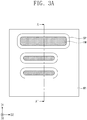
- layout patterns LP1 and LP2 may be provided.
- the layout patterns LP1 and LP2 may correspond to an ideal design of a layer, such as a metal layer, of a semiconductor device.
- the layout patterns LP1 and LP2 may include first layout patterns LP1 and second layout patterns LP2.
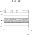
- a target layer TG, a hardmask layer HM, a first mask layer M1, and a second mask layer M2 may be sequentially formed on a substrate 100.
- the substrate 100 may be or include a crystalline semiconductor substrate.
- the substrate 100 may be one of a silicon substrate, a germanium substrate, a silicon-germanium substrate, and a compound semiconductor substrate.
- the hardmask layer HM may be formed of, for example, titanium nitride (TiN).
- the target layer TG may be, for example, an insulating layer, such as silicon nitride (SiN) or silicon oxide (SiO 2 ) or may be a conductive layer (e.g., doped polysilicon).
- the first mask layer M1 may be formed of, for example, one or more of an amorphous silicon layer, a spin-on-hardmask (SOH) layer, a spin-on-glass (SOG) layer, a silicon nitride (SiN) layer, a silicon oxycarbonitride (SiOCN) layer, a silicon carbonitride (SiCN) layer, and a tin oxide (SnOx) layer.
- the second mask layer M2 may be formed of, for example, one or more of a silicon-containing antireflection coating (SiARC) layer, a spin-on-hardmask (SOH) layer, and an amorphous carbon layer.
- Spacers SP may be formed on sidewalls of the patterned first mask layer M1.
- the formation of the spacers SP may include conformally forming a spacer layer on an entire surface of the substrate 100 and performing an anisotropic etching process on the spacer layer.
- the spacers SP may be formed of, for example, one or more of titanium oxide (TiOx), silicon oxide (SiOx), silicon nitride (SiN), silicon oxynitride (SiON), aluminum oxide (AlOx), and tin oxide (SnOx).
- a first filling layer FL1 may be formed on the entire surface of the substrate 100.
- the first filling layer FL1 may include a spin-on-hardmask (SOH) layer.
- SOH spin-on-hardmask
- the first filling layer FL1 may have a flat (e.g., planar) upper surface.
- the spacers SP may be used to pattern the first mask layer M1 in a self-alignment manner. Although openings OP1 and OP2 may have overlapping footprints on first mask layer M1, spacers SP may act to separate the portions of the first mask layer M1 exposed via patterning processes using openings OP1 and OP2, as shown in FIG. 5A .
- a removal process may be performed to remove the second photoresist pattern PR2 and the first filling layer FL1 that remain after the second patterning process.
- a third patterning process may be performed using the spacers SP and the first mask layer M1 as a mask.
- the performing of the third patterning process may include using the spacers SP and the first mask layer M1 as a mask to pattern the hardmask layer HM, and then using the patterned hardmask layer HM as a mask to pattern the target layer TG.
- a removal process may be performed on remaining portions of the spacers SP, the first mask layer M1 and the hardmask layer HM.
- a metal layer may be formed to fill openings of the patterned target layer TG.
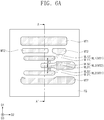
- the first metal patterns MT1 may include a first metal line ML1 and a second metal line ML2.
- the first and second metal lines ML1 and ML2 may extend in a second direction D2.
- the first and second metal lines ML1 and ML2 may extend in parallel to each other.
- the first metal line ML1 may include a first segment ML11 and a second segment ML12.
- the first segment ML11 may extend in the second direction D2.
- the second segment ML12 may be positioned at an end of the first metal line ML1.
- the second segment ML12 may have a width in a first direction D1 that decreases with increasing distance in the second direction D2 from the first segment ML11.
- the second metal line ML2 may include a third segment ML21 and a fourth segment ML22.
- the third segment ML21 may extend in the second direction D2.
- the fourth segment ML22 may be positioned at an end of the second metal line ML2.
- the fourth segment ML22 may have a width in the first direction D1 that decreases with increasing distance in the second direction D2 from the third segment ML21.
- the third metal line ML3 may include a fifth segment ML31 and a sixth segment ML32.
- the fifth segment ML31 may extend in the second direction D2, and may be adjacent both to the first segment ML11 of the first metal line ML1 and to the third segment ML21 of the second metal line ML2.
- the sixth segment ML32 may be adjacent both to the second segment ML12 of the first metal line ML1 and to the fourth segment ML22 of the second metal line ML2.
- the sixth segment ML32 may have a width in the first direction D1 that increases with increasing distance in the second direction D2 from the fifth segment ML31.
- first segment ML11 of the first metal line ML1, the third segment ML21 of the second metal line ML2, and the fifth segment ML31 of the third metal line ML3 may have substantially the same width in the first direction D1.
- a minimum distance between the first segment ML11 of the first metal line ML1 and the fifth segment ML31 of the third metal line ML3 may be substantially the same as a minimum distance between the second segment ML12 of the first metal line ML1 and the sixth segment ML32 of the third metal line ML3.
- a minimum distance between the third segment ML21 of the second metal line ML2 and the fifth segment ML31 of the third metal line ML3 may be substantially the same as a minimum distance between the fourth segment ML22 of the second metal line ML2 and the sixth segment ML32 of the third metal line ML3.
- widths of the first metal lines may be the substantially the same and widths of the second metal lines may be substantially the same, which may be the same or different than (e.g., greater than) the widths of the first metal lines. Distances between immediately neighboring metal lines of this group of metal lines may be substantially the same.
- FIG. 6B illustrates an example of this configuration, with respect to the four metal lines (including ML1, ML2, ML3 and a metal line formed of above ML1 in FIG. 6A along the A'A' cross section) disposed between the leftmost first metal pattern MT1 and the rightmost second metal pattern MT2. It will be appreciated, however, more than four metal lines may be formed in this configuration.
- FIG. 7 illustrates a plan view showing a layout defining a metal layer of a semiconductor device, according to embodiments of inventive concepts.
- layout patterns LP1, LP2, and LP3 may be provided.
- the layout patterns LP1, LP2 and LP3 may correspond to an ideal design of a layer of a semiconductor device.
- the layout patterns LP1, LP2, and LP3 may include first layout patterns LP1, second layout patterns LP2, and third layout patterns LP3.
- the second layout patterns LP2 may overlap the first layout patterns LP1.
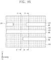
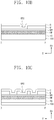
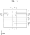
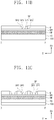
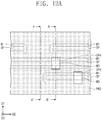
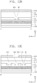
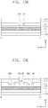
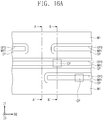
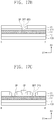
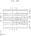
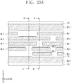
- FIGS. 8A to 23A illustrate plan views showing a method of manufacturing a semiconductor device, according to embodiments of inventive concepts.
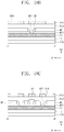
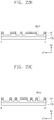
- FIGS. 8B to 23B illustrate cross-sectional views taken along line A-A' of FIGS. 8A to 23A , respectively.
- FIGS. 8C to 23C illustrate cross-sectional views taken along line B-B' of FIGS. 8A to 23A , respectively.
- FIG. 20D illustrates an enlarged view showing section A of FIG. 20C .
- a target layer TG, a hardmask layer HM, a first memory layer MR1, a first mask layer M1, and a second mask layer M2 may be sequentially formed on a substrate 100.
- the substrate 100 may be or include a crystalline semiconductor substrate.
- the substrate 100 may be one of a silicon substrate, a germanium substrate, a silicon-germanium substrate, and a compound semiconductor substrate.
- the target layer TG may be, for example, an insulating layer, such as silicon nitride (SiN) or silicon oxide (SiO 2 ) or may be a conductive layer (e.g., doped polysilicon).
- the hardmask layer HM may be formed of, for example, titanium nitride (TiN).
- the first memory layer MR1 may be formed of, for example, silicon oxide.
- the first mask layer M1 may formed of, for example, one or more of an amorphous silicon layer, a spin-on-hardmask (SOH) layer, a spin-on-glass (SOG) layer, a silicon nitride (SiN) layer, a silicon oxycarbonitride (SiOCN) layer, a silicon carbonitride (SiCN) layer, and a tin oxide (SnOx) layer.
- the second mask layer M2 may include, for example, one or more of a silicon-containing antireflection coating (SiARC) layer, a spin-on-hardmask (SOH) layer, and an amorphous carbon layer.
- Each of the second openings OP2 of the patterned first mask layer M1 may have a second width W2 in the first direction D1.
- a pull-back process may be performed on the patterned first mask layer M1.
- the pull-back process may include a dry etching process or a wet etching process.
- the pull-back process may etch into sidewalls of the initially patterned first mask layer M1.
- openings may be initially formed in the first mask layer M1 by performing an anisotropic etch using the first photoresist pattern PR1 as a mask to pattern the second mask layer M2, and then performing an anisotropic etch using the patterned second mask layer M2 as a mask to pattern the first mask layer M1.
- a protective layer may further be formed on the first mask layer M1.
- the protective layer may cover a top surface of the first mask layer M1.
- the protective layer may prevent the top surface of the first mask layer M1 from being etched when sidewalls of the first mask layer M1 are etched during the pull-back process.
- a first etching process may be performed on the spacer layer SL to remove a portion of the spacer layer SL.
- the first etching process on the spacer layer SL may be an anisotropic etching process.
- spacers SP may be formed on the sidewalls of the first mask layer M1.
- the spacers SP may be formed in the second openings OP2 of the first mask layer M1 and define third openings OP3.
- the third opening OP3 may be surrounded by a corresponding spacer SP.
- the first filling layer FL1 may be removed to form the fifth openings OP5 and the sixth openings OP6.
- a planarization process may be performed to remove a portion of the second filling layer FL2.
- the planarization process may include a chemical mechanical polishing (CMP) process and/or an etch-back process.
- CMP chemical mechanical polishing
- a CMP process may be performed to remove the second filling layer FL2 until the top surface of the second memory layer MR2 is exposed.
- the structure resulting after this CMP process may include a discrete portion of the second filling layer FL2 positioned within the second opening OP2 with respect to a plan view (see FIG. 15A and 10A ) filling a fifth opening OP5 and a sixth opening OP6.
- a cut pattern CP may thus be formed.
- the cut pattern CP may be formed by a remaining portion of the second filling layer FL2 formed within the fifth opening OP5 and sixth opening OP6.
- the cut pattern CP may have a top surface lower than that of the first filling layer FL1.
- the cut pattern CP may completely fill the sixth opening OP6.
- the cut pattern CP may have a top surface higher than and cover the spacer SP that defines the sixth opening OP6 in which it is formed.
- a second etching process may be performed to remove the second memory layer MR2 and the first filling layer FL1.
- the first filling layer FL1 may thus be removed from the third openings OP3.
- the third openings OP3 may be opened again. Since each of the sixth openings OP6 is filled with the cut pattern CP, the sixth openings OP6 may not be opened.
- a third filling layer FL3 may be formed on the entire surface of the substrate 100.
- the third filling layer FL3 may fill the seventh openings OP7.
- the third filling layer FL3 may be patterned with the fourth patterning process to form ninth openings OP9 in the third filling layer FL3, each corresponding to one of the eighth openings OP8 in the third photoresist pattern PR3 .
- Each of the ninth openings OP9 of the third filling layer FL3 may have a third width W3 in the first direction D1. Portions of the ninth openings OP9 of the third filling layer FL3 may vertically overlap the spacers SP.
- ninth openings OP9 of the third filling layer FL3 may have substantially the same shape and size as that of the eighth openings OP8 of the third photoresist pattern PR3.
- a fifth patterning process may be performed using the third filling layer FL3 and the spacers SP as a mask.
- performing the fifth patterning process may include using the patterned third filling layer FL3 and the patterned spacers SP as a mask to pattern the first mask layer M1 with an anisotropic etch, and then using the patterned first mask layer M1 as a mask to pattern the first memory layer MR1 with an anisotropic etch.
- openings referenced herein may be with respect to a particular layer and may be considered to exist even after such openings are later filled.
- the memory layers referenced herein need not form a part of a memory circuit, a memory cell or any part of a memory device, but may refer to layers that may be used obtain a pattern having been formed in another layer of the semiconductor device.
Landscapes
- Exposure Of Semiconductors, Excluding Electron Or Ion Beam Exposure (AREA)
- Semiconductor Memories (AREA)
- Internal Circuitry In Semiconductor Integrated Circuit Devices (AREA)
- Photosensitive Polymer And Photoresist Processing (AREA)
- Drying Of Semiconductors (AREA)
- Physics & Mathematics (AREA)
- Geometry (AREA)
Applications Claiming Priority (1)
| Application Number | Priority Date | Filing Date | Title |
|---|---|---|---|
| KR1020180041021A KR102617139B1 (ko) | 2018-04-09 | 2018-04-09 | 반도체 소자 및 그 제조방법 |
Publications (3)
| Publication Number | Publication Date |
|---|---|
| EP3553810A2 true EP3553810A2 (fr) | 2019-10-16 |
| EP3553810A3 EP3553810A3 (fr) | 2020-07-01 |
| EP3553810B1 EP3553810B1 (fr) | 2024-01-17 |
Family
ID=65724177
Family Applications (1)
| Application Number | Title | Priority Date | Filing Date |
|---|---|---|---|
| EP19160999.9A Active EP3553810B1 (fr) | 2018-04-09 | 2019-03-06 | Dispositif à semiconducteurs et son procédé de fabrication utilisant un masque espaceur |
Country Status (6)
| Country | Link |
|---|---|
| US (1) | US10468252B2 (fr) |
| EP (1) | EP3553810B1 (fr) |
| JP (1) | JP7410648B2 (fr) |
| KR (1) | KR102617139B1 (fr) |
| CN (1) | CN110364432B (fr) |
| SG (1) | SG10201901761VA (fr) |
Families Citing this family (8)
| Publication number | Priority date | Publication date | Assignee | Title |
|---|---|---|---|---|
| US11069564B2 (en) * | 2019-04-09 | 2021-07-20 | International Business Machines Corporation | Double metal patterning |
| KR102811051B1 (ko) * | 2019-10-28 | 2025-05-21 | 삼성전자주식회사 | 패턴 형성을 위한 포토마스크 세트의 제조 방법 및 이를 이용한 반도체 소자의 제조 방법 |
| US11177160B2 (en) * | 2020-03-24 | 2021-11-16 | International Business Machines Corporation | Double patterned lithography using spacer assisted cuts for patterning steps |
| US12283484B2 (en) * | 2020-07-02 | 2025-04-22 | Applied Materials, Inc. | Selective deposition of carbon on photoresist layer for lithography applications |
| CN114078712B (zh) * | 2020-08-19 | 2025-10-10 | 华邦电子股份有限公司 | 半导体结构及其制造方法 |
| US12218007B2 (en) * | 2020-09-30 | 2025-02-04 | Taiwan Semiconductor Manufacturing Co., Ltd. | Self-aligned via formation using spacers |
| CN114496928B (zh) * | 2020-11-11 | 2026-03-17 | 中国科学院微电子研究所 | 一种电容器孔和dram的制造方法 |
| KR20220099616A (ko) | 2021-01-06 | 2022-07-14 | 삼성전자주식회사 | 반도체 소자 및 그의 제조 방법 |
Family Cites Families (28)
| Publication number | Priority date | Publication date | Assignee | Title |
|---|---|---|---|---|
| KR100842763B1 (ko) * | 2007-03-19 | 2008-07-01 | 주식회사 하이닉스반도체 | 반도체 소자의 미세 패턴 형성 방법 |
| KR101428820B1 (ko) * | 2007-05-14 | 2014-08-08 | 마이크론 테크놀로지, 인크. | 토포그래피 지향 패터닝 |
| KR100876892B1 (ko) * | 2007-06-29 | 2009-01-07 | 주식회사 하이닉스반도체 | 반도체 소자의 제조방법 |
| US8048762B2 (en) | 2008-08-25 | 2011-11-01 | Elpida Memory, Inc. | Manufacturing method of semiconductor device |
| KR101532012B1 (ko) | 2008-12-24 | 2015-06-30 | 삼성전자주식회사 | 반도체 소자 및 반도체 소자의 패턴 형성 방법 |
| KR20100080243A (ko) * | 2008-12-31 | 2010-07-08 | 주식회사 동부하이텍 | 반도체 소자 및 그 제조 방법 |
| JP4825891B2 (ja) * | 2009-03-31 | 2011-11-30 | 株式会社東芝 | 半導体装置の製造方法およびテンプレート |
| JP5395837B2 (ja) * | 2011-03-24 | 2014-01-22 | 株式会社東芝 | 半導体装置の製造方法 |
| TWI488238B (zh) * | 2012-03-29 | 2015-06-11 | 力晶科技股份有限公司 | 一種半導體線路製程 |
| KR101926418B1 (ko) * | 2012-05-16 | 2018-12-10 | 삼성전자주식회사 | 반도체 소자의 제조 방법 |
| JP2014072226A (ja) | 2012-09-27 | 2014-04-21 | Tokyo Electron Ltd | パターン形成方法 |
| US8987142B2 (en) * | 2013-01-09 | 2015-03-24 | Taiwan Semiconductor Manufacturing Co., Ltd. | Multi-patterning method and device formed by the method |
| US9069249B2 (en) | 2013-02-01 | 2015-06-30 | Taiwan Semiconductor Manufacturing Company, Ltd. | Self aligned patterning with multiple resist layers |
| US9153478B2 (en) | 2013-03-15 | 2015-10-06 | Taiwan Semiconductor Manufacturing Company, Ltd. | Spacer etching process for integrated circuit design |
| US9093378B2 (en) | 2013-03-15 | 2015-07-28 | Samsung Electronics Co., Ltd. | Method for forming patterns of semiconductor device using SADP process |
| US9209076B2 (en) * | 2013-11-22 | 2015-12-08 | Taiwan Semiconductor Manufacturing Company, Ltd. | Method of double patterning lithography process using plurality of mandrels for integrated circuit applications |
| US9177797B2 (en) | 2013-12-04 | 2015-11-03 | Taiwan Semiconductor Manufacturing Company, Ltd. | Lithography using high selectivity spacers for pitch reduction |
| US9129906B2 (en) * | 2013-12-05 | 2015-09-08 | Taiwan Semiconductor Manufacturing Company, Ltd. | Self-aligned double spacer patterning process |
| US9368349B2 (en) | 2014-01-14 | 2016-06-14 | Taiwan Semiconductor Manufacturing Co., Ltd. | Cut last self-aligned litho-etch patterning |
| US9425049B2 (en) | 2014-01-14 | 2016-08-23 | Taiwan Semiconductor Manufacturing Co., Ltd. | Cut first self-aligned litho-etch patterning |
| US9406511B2 (en) * | 2014-07-10 | 2016-08-02 | Taiwan Semiconductor Manufacturing Company, Ltd. | Self-aligned double patterning |
| KR102192350B1 (ko) * | 2014-08-05 | 2020-12-18 | 삼성전자주식회사 | 반도체 소자의 미세 패턴 형성 방법 및 이를 이용한 반도체 소자의 제조방법 |
| US9754785B2 (en) * | 2015-01-14 | 2017-09-05 | Samsung Electronics Co., Ltd. | Methods of manufacturing semiconductor devices |
| KR102370284B1 (ko) | 2015-07-24 | 2022-03-07 | 에스케이하이닉스 주식회사 | 반도체장치의 패턴 형성 방법 |
| US9490136B1 (en) | 2015-08-31 | 2016-11-08 | Taiwan Semiconductor Manufacturing Company, Ltd. | Method of forming trench cut |
| WO2017111924A1 (fr) * | 2015-12-21 | 2017-06-29 | Intel Corporation | Bouchons et coupes à base de grillage servant à la formation d'extrémité d'élément destiné à des interconnexions d'unité de fabrication finale (beol), et structures ainsi obtenues |
| US10366890B2 (en) * | 2016-05-23 | 2019-07-30 | Tokyo Electron Limited | Method for patterning a substrate using a layer with multiple materials |
| US9786554B1 (en) | 2016-06-08 | 2017-10-10 | International Business Machines Corporation | Self aligned conductive lines |
-
2018
- 2018-04-09 KR KR1020180041021A patent/KR102617139B1/ko active Active
- 2018-11-09 US US16/185,137 patent/US10468252B2/en active Active
-
2019
- 2019-02-27 SG SG10201901761V patent/SG10201901761VA/en unknown
- 2019-03-06 EP EP19160999.9A patent/EP3553810B1/fr active Active
- 2019-03-14 CN CN201910193558.9A patent/CN110364432B/zh active Active
- 2019-03-26 JP JP2019058272A patent/JP7410648B2/ja active Active
Non-Patent Citations (1)
| Title |
|---|
| None |
Also Published As
| Publication number | Publication date |
|---|---|
| US20190311902A1 (en) | 2019-10-10 |
| JP2019186538A (ja) | 2019-10-24 |
| KR102617139B1 (ko) | 2023-12-26 |
| EP3553810B1 (fr) | 2024-01-17 |
| SG10201901761VA (en) | 2019-11-28 |
| US10468252B2 (en) | 2019-11-05 |
| JP7410648B2 (ja) | 2024-01-10 |
| KR20190117984A (ko) | 2019-10-17 |
| CN110364432A (zh) | 2019-10-22 |
| CN110364432B (zh) | 2024-01-16 |
| EP3553810A3 (fr) | 2020-07-01 |
Similar Documents
| Publication | Publication Date | Title |
|---|---|---|
| EP3553810B1 (fr) | Dispositif à semiconducteurs et son procédé de fabrication utilisant un masque espaceur | |
| EP1864320B1 (fr) | Fabrication de circuit integre | |
| US8609324B2 (en) | Method of forming pitch multiplied contacts | |
| CN114068552B (zh) | 半导体器件以及制造该半导体器件的方法 | |
| JP2010536176A (ja) | 緊密なピッチのコンタクトを含む半導体構造体、ならびにその形成方法 | |
| US7074718B2 (en) | Method of fabricating a semiconductor device having a buried and enlarged contact hole | |
| US8647949B2 (en) | Structure and method of fabricating a transistor having a trench gate | |
| US20240332060A1 (en) | Semiconductor device | |
| CN114373712B (zh) | 半导体结构及其形成方法 | |
| US20210280430A1 (en) | Semiconductor memory structure and method for forming the same | |
| CN113363203A (zh) | 半导体器件的形成方法 | |
| US20080242100A1 (en) | Semiconductor device and fabrications thereof | |
| CN113013142A (zh) | 集成芯片 | |
| CN113113405A (zh) | 半导体装置 | |
| CN113363217B (zh) | 半导体存储器结构及其形成方法 | |
| KR100866964B1 (ko) | 반도체 소자 제조를 위한 상호 연결된 미세 하드마스크패턴 형성 방법 | |
| US20040238482A1 (en) | Method for fabricating semiconductor device | |
| CN117116745A (zh) | 半导体结构的形成方法及掩膜版 | |
| CN118098936A (zh) | 半导体结构的制作方法、掩膜结构及半导体结构 | |
| CN1979802A (zh) | 导线的制造方法以及缩小导线与图案间距的方法 |
Legal Events
| Date | Code | Title | Description |
|---|---|---|---|
| PUAI | Public reference made under article 153(3) epc to a published international application that has entered the european phase |
Free format text: ORIGINAL CODE: 0009012 |
|
| STAA | Information on the status of an ep patent application or granted ep patent |
Free format text: STATUS: THE APPLICATION HAS BEEN PUBLISHED |
|
| AK | Designated contracting states |
Kind code of ref document: A2 Designated state(s): AL AT BE BG CH CY CZ DE DK EE ES FI FR GB GR HR HU IE IS IT LI LT LU LV MC MK MT NL NO PL PT RO RS SE SI SK SM TR |
|
| AX | Request for extension of the european patent |
Extension state: BA ME |
|
| PUAL | Search report despatched |
Free format text: ORIGINAL CODE: 0009013 |
|
| AK | Designated contracting states |
Kind code of ref document: A3 Designated state(s): AL AT BE BG CH CY CZ DE DK EE ES FI FR GB GR HR HU IE IS IT LI LT LU LV MC MK MT NL NO PL PT RO RS SE SI SK SM TR |
|
| AX | Request for extension of the european patent |
Extension state: BA ME |
|
| RIC1 | Information provided on ipc code assigned before grant |
Ipc: H01L 21/033 20060101AFI20191220BHEP Ipc: H01L 21/3213 20060101ALN20191220BHEP |
|
| PUAF | Information related to the publication of a search report (a3 document) modified or deleted |
Free format text: ORIGINAL CODE: 0009199SEPU |
|
| D17D | Deferred search report published (deleted) | ||
| PUAL | Search report despatched |
Free format text: ORIGINAL CODE: 0009013 |
|
| RIC1 | Information provided on ipc code assigned before grant |
Ipc: H01L 21/3213 20060101ALN20200514BHEP Ipc: H01L 21/033 20060101AFI20200514BHEP |
|
| RIC1 | Information provided on ipc code assigned before grant |
Ipc: H01L 21/033 20060101AFI20200518BHEP Ipc: H01L 21/3213 20060101ALN20200518BHEP |
|
| AK | Designated contracting states |
Kind code of ref document: A3 Designated state(s): AL AT BE BG CH CY CZ DE DK EE ES FI FR GB GR HR HU IE IS IT LI LT LU LV MC MK MT NL NO PL PT RO RS SE SI SK SM TR |
|
| AX | Request for extension of the european patent |
Extension state: BA ME |
|
| RIC1 | Information provided on ipc code assigned before grant |
Ipc: H01L 21/3213 20060101ALN20200527BHEP Ipc: H01L 21/033 20060101AFI20200527BHEP |
|
| STAA | Information on the status of an ep patent application or granted ep patent |
Free format text: STATUS: REQUEST FOR EXAMINATION WAS MADE |
|
| 17P | Request for examination filed |
Effective date: 20201223 |
|
| RBV | Designated contracting states (corrected) |
Designated state(s): AL AT BE BG CH CY CZ DE DK EE ES FI FR GB GR HR HU IE IS IT LI LT LU LV MC MK MT NL NO PL PT RO RS SE SI SK SM TR |
|
| P01 | Opt-out of the competence of the unified patent court (upc) registered |
Effective date: 20230520 |
|
| REG | Reference to a national code |
Ref country code: DE Ref legal event code: R079 Free format text: PREVIOUS MAIN CLASS: H01L0021033000 Ipc: H01L0021311000 Ref document number: 602019045118 Country of ref document: DE |
|
| GRAP | Despatch of communication of intention to grant a patent |
Free format text: ORIGINAL CODE: EPIDOSNIGR1 |
|
| STAA | Information on the status of an ep patent application or granted ep patent |
Free format text: STATUS: GRANT OF PATENT IS INTENDED |
|
| RIC1 | Information provided on ipc code assigned before grant |
Ipc: H01L 21/3213 20060101ALI20230711BHEP Ipc: H01L 21/768 20060101ALI20230711BHEP Ipc: H01L 21/321 20060101ALI20230711BHEP Ipc: H01L 21/033 20060101ALI20230711BHEP Ipc: H01L 21/311 20060101AFI20230711BHEP |
|
| INTG | Intention to grant announced |
Effective date: 20230803 |
|
| GRAS | Grant fee paid |
Free format text: ORIGINAL CODE: EPIDOSNIGR3 |
|
| GRAA | (expected) grant |
Free format text: ORIGINAL CODE: 0009210 |
|
| STAA | Information on the status of an ep patent application or granted ep patent |
Free format text: STATUS: THE PATENT HAS BEEN GRANTED |
|
| AK | Designated contracting states |
Kind code of ref document: B1 Designated state(s): AL AT BE BG CH CY CZ DE DK EE ES FI FR GB GR HR HU IE IS IT LI LT LU LV MC MK MT NL NO PL PT RO RS SE SI SK SM TR |
|
| REG | Reference to a national code |
Ref country code: GB Ref legal event code: FG4D |
|
| REG | Reference to a national code |
Ref country code: CH Ref legal event code: EP |
|
| REG | Reference to a national code |
Ref country code: DE Ref legal event code: R096 Ref document number: 602019045118 Country of ref document: DE |
|
| REG | Reference to a national code |
Ref country code: IE Ref legal event code: FG4D |
|
| REG | Reference to a national code |
Ref country code: NL Ref legal event code: FP |
|
| REG | Reference to a national code |
Ref country code: LT Ref legal event code: MG9D |
|
| REG | Reference to a national code |
Ref country code: AT Ref legal event code: MK05 Ref document number: 1651115 Country of ref document: AT Kind code of ref document: T Effective date: 20240117 |
|
| PG25 | Lapsed in a contracting state [announced via postgrant information from national office to epo] |
Ref country code: IS Free format text: LAPSE BECAUSE OF FAILURE TO SUBMIT A TRANSLATION OF THE DESCRIPTION OR TO PAY THE FEE WITHIN THE PRESCRIBED TIME-LIMIT Effective date: 20240517 |
|
| PG25 | Lapsed in a contracting state [announced via postgrant information from national office to epo] |
Ref country code: LT Free format text: LAPSE BECAUSE OF FAILURE TO SUBMIT A TRANSLATION OF THE DESCRIPTION OR TO PAY THE FEE WITHIN THE PRESCRIBED TIME-LIMIT Effective date: 20240117 |
|
| PG25 | Lapsed in a contracting state [announced via postgrant information from national office to epo] |
Ref country code: GR Free format text: LAPSE BECAUSE OF FAILURE TO SUBMIT A TRANSLATION OF THE DESCRIPTION OR TO PAY THE FEE WITHIN THE PRESCRIBED TIME-LIMIT Effective date: 20240418 |
|
| PG25 | Lapsed in a contracting state [announced via postgrant information from national office to epo] |
Ref country code: RS Free format text: LAPSE BECAUSE OF FAILURE TO SUBMIT A TRANSLATION OF THE DESCRIPTION OR TO PAY THE FEE WITHIN THE PRESCRIBED TIME-LIMIT Effective date: 20240417 Ref country code: HR Free format text: LAPSE BECAUSE OF FAILURE TO SUBMIT A TRANSLATION OF THE DESCRIPTION OR TO PAY THE FEE WITHIN THE PRESCRIBED TIME-LIMIT Effective date: 20240117 |
|
| PG25 | Lapsed in a contracting state [announced via postgrant information from national office to epo] |
Ref country code: ES Free format text: LAPSE BECAUSE OF FAILURE TO SUBMIT A TRANSLATION OF THE DESCRIPTION OR TO PAY THE FEE WITHIN THE PRESCRIBED TIME-LIMIT Effective date: 20240117 |
|
| PG25 | Lapsed in a contracting state [announced via postgrant information from national office to epo] |
Ref country code: AT Free format text: LAPSE BECAUSE OF FAILURE TO SUBMIT A TRANSLATION OF THE DESCRIPTION OR TO PAY THE FEE WITHIN THE PRESCRIBED TIME-LIMIT Effective date: 20240117 |
|
| PG25 | Lapsed in a contracting state [announced via postgrant information from national office to epo] |
Ref country code: RS Free format text: LAPSE BECAUSE OF FAILURE TO SUBMIT A TRANSLATION OF THE DESCRIPTION OR TO PAY THE FEE WITHIN THE PRESCRIBED TIME-LIMIT Effective date: 20240417 Ref country code: NO Free format text: LAPSE BECAUSE OF FAILURE TO SUBMIT A TRANSLATION OF THE DESCRIPTION OR TO PAY THE FEE WITHIN THE PRESCRIBED TIME-LIMIT Effective date: 20240417 Ref country code: LT Free format text: LAPSE BECAUSE OF FAILURE TO SUBMIT A TRANSLATION OF THE DESCRIPTION OR TO PAY THE FEE WITHIN THE PRESCRIBED TIME-LIMIT Effective date: 20240117 Ref country code: IS Free format text: LAPSE BECAUSE OF FAILURE TO SUBMIT A TRANSLATION OF THE DESCRIPTION OR TO PAY THE FEE WITHIN THE PRESCRIBED TIME-LIMIT Effective date: 20240517 Ref country code: HR Free format text: LAPSE BECAUSE OF FAILURE TO SUBMIT A TRANSLATION OF THE DESCRIPTION OR TO PAY THE FEE WITHIN THE PRESCRIBED TIME-LIMIT Effective date: 20240117 Ref country code: GR Free format text: LAPSE BECAUSE OF FAILURE TO SUBMIT A TRANSLATION OF THE DESCRIPTION OR TO PAY THE FEE WITHIN THE PRESCRIBED TIME-LIMIT Effective date: 20240418 Ref country code: FI Free format text: LAPSE BECAUSE OF FAILURE TO SUBMIT A TRANSLATION OF THE DESCRIPTION OR TO PAY THE FEE WITHIN THE PRESCRIBED TIME-LIMIT Effective date: 20240117 Ref country code: ES Free format text: LAPSE BECAUSE OF FAILURE TO SUBMIT A TRANSLATION OF THE DESCRIPTION OR TO PAY THE FEE WITHIN THE PRESCRIBED TIME-LIMIT Effective date: 20240117 Ref country code: BG Free format text: LAPSE BECAUSE OF FAILURE TO SUBMIT A TRANSLATION OF THE DESCRIPTION OR TO PAY THE FEE WITHIN THE PRESCRIBED TIME-LIMIT Effective date: 20240117 Ref country code: AT Free format text: LAPSE BECAUSE OF FAILURE TO SUBMIT A TRANSLATION OF THE DESCRIPTION OR TO PAY THE FEE WITHIN THE PRESCRIBED TIME-LIMIT Effective date: 20240117 |
|
| PG25 | Lapsed in a contracting state [announced via postgrant information from national office to epo] |
Ref country code: PL Free format text: LAPSE BECAUSE OF FAILURE TO SUBMIT A TRANSLATION OF THE DESCRIPTION OR TO PAY THE FEE WITHIN THE PRESCRIBED TIME-LIMIT Effective date: 20240117 Ref country code: PT Free format text: LAPSE BECAUSE OF FAILURE TO SUBMIT A TRANSLATION OF THE DESCRIPTION OR TO PAY THE FEE WITHIN THE PRESCRIBED TIME-LIMIT Effective date: 20240517 |
|
| PG25 | Lapsed in a contracting state [announced via postgrant information from national office to epo] |
Ref country code: SE Free format text: LAPSE BECAUSE OF FAILURE TO SUBMIT A TRANSLATION OF THE DESCRIPTION OR TO PAY THE FEE WITHIN THE PRESCRIBED TIME-LIMIT Effective date: 20240117 Ref country code: PT Free format text: LAPSE BECAUSE OF FAILURE TO SUBMIT A TRANSLATION OF THE DESCRIPTION OR TO PAY THE FEE WITHIN THE PRESCRIBED TIME-LIMIT Effective date: 20240517 Ref country code: PL Free format text: LAPSE BECAUSE OF FAILURE TO SUBMIT A TRANSLATION OF THE DESCRIPTION OR TO PAY THE FEE WITHIN THE PRESCRIBED TIME-LIMIT Effective date: 20240117 Ref country code: LV Free format text: LAPSE BECAUSE OF FAILURE TO SUBMIT A TRANSLATION OF THE DESCRIPTION OR TO PAY THE FEE WITHIN THE PRESCRIBED TIME-LIMIT Effective date: 20240117 |
|
| PG25 | Lapsed in a contracting state [announced via postgrant information from national office to epo] |
Ref country code: DK Free format text: LAPSE BECAUSE OF FAILURE TO SUBMIT A TRANSLATION OF THE DESCRIPTION OR TO PAY THE FEE WITHIN THE PRESCRIBED TIME-LIMIT Effective date: 20240117 |
|
| PG25 | Lapsed in a contracting state [announced via postgrant information from national office to epo] |
Ref country code: SM Free format text: LAPSE BECAUSE OF FAILURE TO SUBMIT A TRANSLATION OF THE DESCRIPTION OR TO PAY THE FEE WITHIN THE PRESCRIBED TIME-LIMIT Effective date: 20240117 |
|
| REG | Reference to a national code |
Ref country code: DE Ref legal event code: R097 Ref document number: 602019045118 Country of ref document: DE |
|
| PG25 | Lapsed in a contracting state [announced via postgrant information from national office to epo] |
Ref country code: CZ Free format text: LAPSE BECAUSE OF FAILURE TO SUBMIT A TRANSLATION OF THE DESCRIPTION OR TO PAY THE FEE WITHIN THE PRESCRIBED TIME-LIMIT Effective date: 20240117 Ref country code: EE Free format text: LAPSE BECAUSE OF FAILURE TO SUBMIT A TRANSLATION OF THE DESCRIPTION OR TO PAY THE FEE WITHIN THE PRESCRIBED TIME-LIMIT Effective date: 20240117 |
|
| PG25 | Lapsed in a contracting state [announced via postgrant information from national office to epo] |
Ref country code: SK Free format text: LAPSE BECAUSE OF FAILURE TO SUBMIT A TRANSLATION OF THE DESCRIPTION OR TO PAY THE FEE WITHIN THE PRESCRIBED TIME-LIMIT Effective date: 20240117 |
|
| PG25 | Lapsed in a contracting state [announced via postgrant information from national office to epo] |
Ref country code: SM Free format text: LAPSE BECAUSE OF FAILURE TO SUBMIT A TRANSLATION OF THE DESCRIPTION OR TO PAY THE FEE WITHIN THE PRESCRIBED TIME-LIMIT Effective date: 20240117 Ref country code: SK Free format text: LAPSE BECAUSE OF FAILURE TO SUBMIT A TRANSLATION OF THE DESCRIPTION OR TO PAY THE FEE WITHIN THE PRESCRIBED TIME-LIMIT Effective date: 20240117 Ref country code: RO Free format text: LAPSE BECAUSE OF FAILURE TO SUBMIT A TRANSLATION OF THE DESCRIPTION OR TO PAY THE FEE WITHIN THE PRESCRIBED TIME-LIMIT Effective date: 20240117 Ref country code: EE Free format text: LAPSE BECAUSE OF FAILURE TO SUBMIT A TRANSLATION OF THE DESCRIPTION OR TO PAY THE FEE WITHIN THE PRESCRIBED TIME-LIMIT Effective date: 20240117 Ref country code: DK Free format text: LAPSE BECAUSE OF FAILURE TO SUBMIT A TRANSLATION OF THE DESCRIPTION OR TO PAY THE FEE WITHIN THE PRESCRIBED TIME-LIMIT Effective date: 20240117 Ref country code: CZ Free format text: LAPSE BECAUSE OF FAILURE TO SUBMIT A TRANSLATION OF THE DESCRIPTION OR TO PAY THE FEE WITHIN THE PRESCRIBED TIME-LIMIT Effective date: 20240117 |
|
| REG | Reference to a national code |
Ref country code: CH Ref legal event code: PL |
|
| PG25 | Lapsed in a contracting state [announced via postgrant information from national office to epo] |
Ref country code: LU Free format text: LAPSE BECAUSE OF NON-PAYMENT OF DUE FEES Effective date: 20240306 |
|
| PG25 | Lapsed in a contracting state [announced via postgrant information from national office to epo] |
Ref country code: MC Free format text: LAPSE BECAUSE OF FAILURE TO SUBMIT A TRANSLATION OF THE DESCRIPTION OR TO PAY THE FEE WITHIN THE PRESCRIBED TIME-LIMIT Effective date: 20240117 |
|
| PLBE | No opposition filed within time limit |
Free format text: ORIGINAL CODE: 0009261 |
|
| STAA | Information on the status of an ep patent application or granted ep patent |
Free format text: STATUS: NO OPPOSITION FILED WITHIN TIME LIMIT |
|
| PG25 | Lapsed in a contracting state [announced via postgrant information from national office to epo] |
Ref country code: MC Free format text: LAPSE BECAUSE OF FAILURE TO SUBMIT A TRANSLATION OF THE DESCRIPTION OR TO PAY THE FEE WITHIN THE PRESCRIBED TIME-LIMIT Effective date: 20240117 Ref country code: LU Free format text: LAPSE BECAUSE OF NON-PAYMENT OF DUE FEES Effective date: 20240306 |
|
| PG25 | Lapsed in a contracting state [announced via postgrant information from national office to epo] |
Ref country code: IT Free format text: LAPSE BECAUSE OF FAILURE TO SUBMIT A TRANSLATION OF THE DESCRIPTION OR TO PAY THE FEE WITHIN THE PRESCRIBED TIME-LIMIT Effective date: 20240117 |
|
| REG | Reference to a national code |
Ref country code: BE Ref legal event code: MM Effective date: 20240331 |
|
| 26N | No opposition filed |
Effective date: 20241018 |
|
| PG25 | Lapsed in a contracting state [announced via postgrant information from national office to epo] |
Ref country code: IT Free format text: LAPSE BECAUSE OF FAILURE TO SUBMIT A TRANSLATION OF THE DESCRIPTION OR TO PAY THE FEE WITHIN THE PRESCRIBED TIME-LIMIT Effective date: 20240117 |
|
| PG25 | Lapsed in a contracting state [announced via postgrant information from national office to epo] |
Ref country code: BE Free format text: LAPSE BECAUSE OF NON-PAYMENT OF DUE FEES Effective date: 20240331 |
|
| PG25 | Lapsed in a contracting state [announced via postgrant information from national office to epo] |
Ref country code: FR Free format text: LAPSE BECAUSE OF NON-PAYMENT OF DUE FEES Effective date: 20240317 |
|
| PG25 | Lapsed in a contracting state [announced via postgrant information from national office to epo] |
Ref country code: IE Free format text: LAPSE BECAUSE OF NON-PAYMENT OF DUE FEES Effective date: 20240306 |
|
| PG25 | Lapsed in a contracting state [announced via postgrant information from national office to epo] |
Ref country code: IE Free format text: LAPSE BECAUSE OF NON-PAYMENT OF DUE FEES Effective date: 20240306 Ref country code: FR Free format text: LAPSE BECAUSE OF NON-PAYMENT OF DUE FEES Effective date: 20240317 Ref country code: BE Free format text: LAPSE BECAUSE OF NON-PAYMENT OF DUE FEES Effective date: 20240331 Ref country code: CH Free format text: LAPSE BECAUSE OF NON-PAYMENT OF DUE FEES Effective date: 20240331 |
|
| PG25 | Lapsed in a contracting state [announced via postgrant information from national office to epo] |
Ref country code: SI Free format text: LAPSE BECAUSE OF FAILURE TO SUBMIT A TRANSLATION OF THE DESCRIPTION OR TO PAY THE FEE WITHIN THE PRESCRIBED TIME-LIMIT Effective date: 20240117 |
|
| PG25 | Lapsed in a contracting state [announced via postgrant information from national office to epo] |
Ref country code: CY Free format text: LAPSE BECAUSE OF FAILURE TO SUBMIT A TRANSLATION OF THE DESCRIPTION OR TO PAY THE FEE WITHIN THE PRESCRIBED TIME-LIMIT; INVALID AB INITIO Effective date: 20190306 |
|
| PG25 | Lapsed in a contracting state [announced via postgrant information from national office to epo] |
Ref country code: HU Free format text: LAPSE BECAUSE OF FAILURE TO SUBMIT A TRANSLATION OF THE DESCRIPTION OR TO PAY THE FEE WITHIN THE PRESCRIBED TIME-LIMIT; INVALID AB INITIO Effective date: 20190306 |
|
| PG25 | Lapsed in a contracting state [announced via postgrant information from national office to epo] |
Ref country code: TR Free format text: LAPSE BECAUSE OF FAILURE TO SUBMIT A TRANSLATION OF THE DESCRIPTION OR TO PAY THE FEE WITHIN THE PRESCRIBED TIME-LIMIT Effective date: 20240117 |
|
| PGFP | Annual fee paid to national office [announced via postgrant information from national office to epo] |
Ref country code: NL Payment date: 20260128 Year of fee payment: 8 |
|
| PGFP | Annual fee paid to national office [announced via postgrant information from national office to epo] |
Ref country code: GB Payment date: 20260128 Year of fee payment: 8 |
|
| PGFP | Annual fee paid to national office [announced via postgrant information from national office to epo] |
Ref country code: DE Payment date: 20260128 Year of fee payment: 8 |