EP3547670B1 - Bildaufnahmevorrichtung und ansteuerungsverfahren für eine bildaufnahmevorrichtung - Google Patents
Bildaufnahmevorrichtung und ansteuerungsverfahren für eine bildaufnahmevorrichtung Download PDFInfo
- Publication number
- EP3547670B1 EP3547670B1 EP19169912.3A EP19169912A EP3547670B1 EP 3547670 B1 EP3547670 B1 EP 3547670B1 EP 19169912 A EP19169912 A EP 19169912A EP 3547670 B1 EP3547670 B1 EP 3547670B1
- Authority
- EP
- European Patent Office
- Prior art keywords
- pixels
- time point
- period
- photoelectric conversion
- charge
- Prior art date
- Legal status (The legal status is an assumption and is not a legal conclusion. Google has not performed a legal analysis and makes no representation as to the accuracy of the status listed.)
- Active
Links
- 238000000034 method Methods 0.000 title claims description 25
- 238000006243 chemical reaction Methods 0.000 claims description 96
- 238000012546 transfer Methods 0.000 claims description 91
- 230000003321 amplification Effects 0.000 claims description 14
- 238000003199 nucleic acid amplification method Methods 0.000 claims description 14
- 238000009825 accumulation Methods 0.000 claims description 11
- 230000004044 response Effects 0.000 claims description 4
- 238000007599 discharging Methods 0.000 claims description 2
- 239000004065 semiconductor Substances 0.000 description 55
- 238000010586 diagram Methods 0.000 description 36
- 230000000694 effects Effects 0.000 description 7
- 239000000758 substrate Substances 0.000 description 7
- 239000012535 impurity Substances 0.000 description 6
- 239000011229 interlayer Substances 0.000 description 6
- 230000003287 optical effect Effects 0.000 description 6
- 230000035945 sensitivity Effects 0.000 description 6
- 238000009792 diffusion process Methods 0.000 description 5
- 238000003384 imaging method Methods 0.000 description 4
- 238000009413 insulation Methods 0.000 description 4
- 239000010410 layer Substances 0.000 description 4
- 238000012545 processing Methods 0.000 description 4
- 230000006870 function Effects 0.000 description 3
- 230000015556 catabolic process Effects 0.000 description 2
- 238000006731 degradation reaction Methods 0.000 description 2
- 239000011159 matrix material Substances 0.000 description 2
- 238000005096 rolling process Methods 0.000 description 2
- 239000007787 solid Substances 0.000 description 2
- 230000001629 suppression Effects 0.000 description 2
- 229910052581 Si3N4 Inorganic materials 0.000 description 1
- VYPSYNLAJGMNEJ-UHFFFAOYSA-N Silicium dioxide Chemical compound O=[Si]=O VYPSYNLAJGMNEJ-UHFFFAOYSA-N 0.000 description 1
- XUIMIQQOPSSXEZ-UHFFFAOYSA-N Silicon Chemical compound [Si] XUIMIQQOPSSXEZ-UHFFFAOYSA-N 0.000 description 1
- 229910000831 Steel Inorganic materials 0.000 description 1
- 229910052782 aluminium Inorganic materials 0.000 description 1
- XAGFODPZIPBFFR-UHFFFAOYSA-N aluminium Chemical compound [Al] XAGFODPZIPBFFR-UHFFFAOYSA-N 0.000 description 1
- 230000004888 barrier function Effects 0.000 description 1
- 230000008901 benefit Effects 0.000 description 1
- 238000004364 calculation method Methods 0.000 description 1
- 230000001413 cellular effect Effects 0.000 description 1
- 230000008859 change Effects 0.000 description 1
- 238000012937 correction Methods 0.000 description 1
- 238000013461 design Methods 0.000 description 1
- 230000006872 improvement Effects 0.000 description 1
- 239000000463 material Substances 0.000 description 1
- 229910052751 metal Inorganic materials 0.000 description 1
- 239000002184 metal Substances 0.000 description 1
- 239000000203 mixture Substances 0.000 description 1
- 238000005457 optimization Methods 0.000 description 1
- 238000005036 potential barrier Methods 0.000 description 1
- 230000008569 process Effects 0.000 description 1
- 230000009467 reduction Effects 0.000 description 1
- 229910052710 silicon Inorganic materials 0.000 description 1
- 239000010703 silicon Substances 0.000 description 1
- HQVNEWCFYHHQES-UHFFFAOYSA-N silicon nitride Chemical compound N12[Si]34N5[Si]62N3[Si]51N64 HQVNEWCFYHHQES-UHFFFAOYSA-N 0.000 description 1
- 229910052814 silicon oxide Inorganic materials 0.000 description 1
- 239000010959 steel Substances 0.000 description 1
- WFKWXMTUELFFGS-UHFFFAOYSA-N tungsten Chemical compound [W] WFKWXMTUELFFGS-UHFFFAOYSA-N 0.000 description 1
- 229910052721 tungsten Inorganic materials 0.000 description 1
- 239000010937 tungsten Substances 0.000 description 1
Images


Classifications
-
- H—ELECTRICITY
- H04—ELECTRIC COMMUNICATION TECHNIQUE
- H04N—PICTORIAL COMMUNICATION, e.g. TELEVISION
- H04N23/00—Cameras or camera modules comprising electronic image sensors; Control thereof
- H04N23/70—Circuitry for compensating brightness variation in the scene
- H04N23/73—Circuitry for compensating brightness variation in the scene by influencing the exposure time
-
- H—ELECTRICITY
- H04—ELECTRIC COMMUNICATION TECHNIQUE
- H04N—PICTORIAL COMMUNICATION, e.g. TELEVISION
- H04N25/00—Circuitry of solid-state image sensors [SSIS]; Control thereof
- H04N25/50—Control of the SSIS exposure
- H04N25/53—Control of the integration time
-
- H—ELECTRICITY
- H04—ELECTRIC COMMUNICATION TECHNIQUE
- H04N—PICTORIAL COMMUNICATION, e.g. TELEVISION
- H04N25/00—Circuitry of solid-state image sensors [SSIS]; Control thereof
- H04N25/50—Control of the SSIS exposure
- H04N25/53—Control of the integration time
- H04N25/531—Control of the integration time by controlling rolling shutters in CMOS SSIS
-
- H—ELECTRICITY
- H04—ELECTRIC COMMUNICATION TECHNIQUE
- H04N—PICTORIAL COMMUNICATION, e.g. TELEVISION
- H04N25/00—Circuitry of solid-state image sensors [SSIS]; Control thereof
- H04N25/70—SSIS architectures; Circuits associated therewith
- H04N25/71—Charge-coupled device [CCD] sensors; Charge-transfer registers specially adapted for CCD sensors
- H04N25/75—Circuitry for providing, modifying or processing image signals from the pixel array
-
- H—ELECTRICITY
- H04—ELECTRIC COMMUNICATION TECHNIQUE
- H04N—PICTORIAL COMMUNICATION, e.g. TELEVISION
- H04N25/00—Circuitry of solid-state image sensors [SSIS]; Control thereof
- H04N25/70—SSIS architectures; Circuits associated therewith
- H04N25/76—Addressed sensors, e.g. MOS or CMOS sensors
-
- H—ELECTRICITY
- H04—ELECTRIC COMMUNICATION TECHNIQUE
- H04N—PICTORIAL COMMUNICATION, e.g. TELEVISION
- H04N25/00—Circuitry of solid-state image sensors [SSIS]; Control thereof
- H04N25/70—SSIS architectures; Circuits associated therewith
- H04N25/76—Addressed sensors, e.g. MOS or CMOS sensors
- H04N25/77—Pixel circuitry, e.g. memories, A/D converters, pixel amplifiers, shared circuits or shared components
- H04N25/771—Pixel circuitry, e.g. memories, A/D converters, pixel amplifiers, shared circuits or shared components comprising storage means other than floating diffusion
Landscapes
- Engineering & Computer Science (AREA)
- Multimedia (AREA)
- Signal Processing (AREA)
- Transforming Light Signals Into Electric Signals (AREA)
- Solid State Image Pick-Up Elements (AREA)
Claims (15)
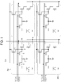
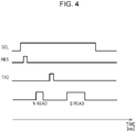
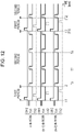
- Bildaufnahmevorrichtung, umfassend:mehrere Pixel (20), wobei die Pixel (20a, 20b) jeweils umfassen: eine Einheit (1) zur photoelektrischen Umwandlung zum Erzeugen von Ladung in Reaktion auf einfallendes Licht und zum Akkumulieren der Ladung, eine Speichereinheit (2) zum Speichern der Ladung, eine Verstärkungseinheit (3, 10) zum Ausgeben eines auf der Ladung basierenden Signals, einen ersten Übertragungsschalter (4) zum Übertragen der Ladung von der Einheit (1) zur photoelektrischen Umwandlung an die Speichereinheit (2), und einen zweiten Übertragungsschalter (5) zum Übertragen der Ladung von der Speichereinheit (2) an die Verstärkereinheit (3, 10); undeine Ausgabeleitung (8), an die Signale von den mehreren Pixeln (20) ausgegeben werden; sowieeine Steuereinheit, die ausgelegt ist, die folgenden Schritte durchzuführen:an einem ersten Zeitpunkt (T1) beginnen die Einheiten (1) zur photoelektrischen Umwandlung der mehreren Pixel (20), Ladung zu akkumulieren,der erste Übertragungsschalter (4) mindestens eines der mehreren Pixel (20) bleibt vom ersten Zeitpunkt (T1) bis zu einem zweiten Zeitpunkt (T2) ausgeschaltet und die Einheit (1) zur photoelektrischen Umwandlung des mindestens einen Pixels der mehreren Pixel (20) akkumuliert Ladung, die in einem ersten Zeitraum vom ersten Zeitpunkt (T1) bis zum zweiten Zeitpunkt (T2) erzeugt wurde,im ersten Zeitraum werden die zweiten Übertragungsschalter (5) der mehreren Pixel (20) angeschaltet und die Verstärkungseinheiten (3, 10) der mehreren Pixel (20) geben abwechselnd die Signale, die auf vor dem ersten Zeitpunkt erzeugten Ladungen basieren, an die Ausgabeleitung (8) aus,in einem zweiten Zeitraum vom zweiten Zeitpunkt (T2) bis zu einem dritten Zeitpunkt (T3) speichern die Speichereinheiten (2) der mehreren Pixel (20) Ladung, die durch die Einheiten (1) zur photoelektrischen Umwandlung im ersten Zeitraum erzeugt und durch die ersten Übertragungsschalter übertragen wurde, undim zweiten Zeitraum wird An/Aus-Steuerung der ersten Übertragungsschalter (4) der mehreren Pixel (20) mehrmals durchgeführt, undam dritten Zeitpunkt (T3) werden die ersten Übertragungsschalter (4) der mehreren Pixel von angeschaltet auf ausgeschaltet gesteuert,wobei:die zweiten Übertragungsschalter (5) der mehreren Pixel (20) vom zweiten Zeitpunkt (T2) bis zum dritten Zeitpunkt (T3) ausgeschaltet bleiben,ein Zeitraum vom ersten Zeitpunkt (T1) bis zum dritten Zeitpunkt (T3) ein Belichtungszeitraum ist, in dem die mehreren Pixel (20) belichtet werden, unddie Bildaufnahmevorrichtung konfiguriert ist, in einem Global-Electronic-Shutter-Modus zu arbeiten, der konfiguriert ist, Aufladen der mehreren Pixel (20) am ersten Zeitpunkt (T1) zu beginnen und die ersten Übertragungsschalter (4) der mehreren Pixel am dritten Zeitpunkt (T3) auszuschalten.
- Bildverarbeitungsvorrichtung nach Anspruch 1,
wobei eine erste Steuerung der Steuerung der ersten Übertragungsschalter (4) von ausgeschaltet auf angeschaltet am Anfang des zweiten Zeitraums durchgeführt wird. - Bildverarbeitungsvorrichtung nach Anspruch 2,
wobei im zweiten Zeitraum die ersten Übertragungsschalter (4) der mehreren Pixel an einem vierten Zeitpunkt (T6) von angeschaltet auf ausgeschaltet gesteuert werden. - Bildaufnahmevorrichtung nach einem der Ansprüche 1 bis 3,
wobei die ersten Übertragungsschalter (4) der mehreren Pixel konfiguriert sind, die in dem Teil des zweiten Zeitraums erzeugte Ladung zu den Speichereinheiten (2) der mehreren Pixel (20) zu übertragen, sodass die Speichereinheiten (2) der mehreren Pixel (20) die durch die Einheiten (1) zur photoelektrischen Umwandlung im ersten Zeitraum erzeugte Ladung und die durch die Einheiten (1) zur photoelektrischen Umwandlung im zweiten Zeitraum erzeugte Ladung speichern. - Bildaufnahmevorrichtung nach einem der Ansprüche 1 bis 4,
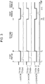
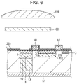
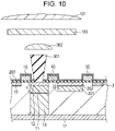
wobei die Bildaufnahmevorrichtung Wellenleiter (301) enthält, die so angeordnet sind, dass sie den Einheiten zur photoelektrischen Umwandlung der mehreren Pixel entsprechen. - Ansteuerverfahren für die Bildaufnahmevorrichtung nach einem der Ansprüche 1 bis 5,
wobei das Verfahren die folgenden Schritte umfasst:zu einem ersten Zeitpunkt (T1) beginnen die Einheiten (1) zur photoelektrischen Umwandlung der mehreren Pixel (20), Ladung zu akkumulieren,der erste Übertragungsschalter (4) mindestens eines der mehreren Pixel (20) bleibt vom ersten Zeitpunkt (T1) bis zu einem zweiten Zeitpunkt (T2) ausgeschaltet und die Einheit (1) zur photoelektrischen Umwandlung des mindestens einen Pixels der mehreren Pixel (20) akkumuliert Ladung, die in einem ersten Zeitraum vom ersten Zeitpunkt (T1) bis zum zweiten Zeitpunkt (T2) erzeugt wurde,im ersten Zeitraum werden die zweiten Übertragungsschalter (5) der mehreren Pixel (20) angeschaltet und die Verstärkungseinheiten (3, 10) der mehreren Pixel (20) geben abwechselnd die Signale, die auf vor dem ersten Zeitpunkt erzeugten Ladungen basieren, an die Ausgabeleitung (8) aus,in einem zweiten Zeitraum vom zweiten Zeitpunkt (T2) bis zu einem dritten Zeitpunkt (T3) speichern die Speichereinheiten (2) der mehreren Pixel (20) Ladung, die durch die Einheiten (1) zur photoelektrischen Umwandlung im ersten Zeitraum erzeugt und durch die ersten Übertragungsschalter übertragen wurde, undim zweiten Zeitraum wird An/Aus-Steuerung der ersten Übertragungsschalter (4) der mehreren Pixel (20) mehrmals durchgeführt, undam dritten Zeitpunkt (T3) werden die ersten Übertragungsschalter (4) der mehreren Pixel (20) von angeschaltet auf ausgeschaltet gesteuert,wobei:die zweiten Übertragungsschalter (5) der mehreren Pixel (20) vom zweiten Zeitpunkt (T2) bis zum dritten Zeitpunkt (T3) ausgeschaltet bleiben,ein Zeitraum vom ersten Zeitpunkt (T1) bis zum dritten Zeitpunkt (T3) ein Belichtungszeitraum ist, in dem die mehreren Pixel (20) belichtet werden, undein Global-Electronic-Shutter-Modus Aufladen der mehreren Pixel (20) an einem ersten Zeitpunkt (T1) beginnt und um die ersten Übertragungsschalter (4) der mehreren Pixel am dritten Zeitpunkt (T3) auszuschalten. - Ansteuerverfahren nach Anspruch 6, wobei ein jeweiliger der mehreren Pixel einen Entladeschalter (18) zum Entladen der Ladung der Einheit zur photoelektrischen Umwandlung umfasst, und
der Entladeschalter des mindestens einen der Pixel vom ersten Zeitpunkt bis zum zweiten Zeitpunkt ausgeschaltet bleibt. - Ansteuerverfahren nach Anspruch 7, wobei das Akkumulieren der Ladung begonnen wird, indem der Entladeschalter von angeschaltet auf ausgeschaltet gesteuert wird.
- Ansteuerverfahren nach Anspruch 6 oder 7, wobei
das Akkumulieren der Ladung begonnen wird, indem der erste Übertragungsschalter von angeschaltet auf ausgeschaltet gesteuert wird. - Ansteuerverfahren nach einem der Ansprüche 6 bis 9, wobeidie ersten Übertragungsschalter der mehreren Pixel spätestens bis zum zweiten Zeitpunkt angeschaltet werden, unddie ersten Übertragungsschalter in einem Abschnitt des zweiten Zeitraums ausgeschaltet werden.
- Ansteuerverfahren nach Anspruch 10, wobei eine erste Steuerung der Steuerung der ersten Übertragungsschalter (4) von ausgeschaltet auf angeschaltet am Anfang des zweiten Zeitraums durchgeführt wird.
- Ansteuerverfahren nach Anspruch 11, wobei
die mehreren Male mehr sind als ein Verhältnis von Sättigungsladungsmenge der Speichereinheit zu Sättigungsladungsmenge der Einheit zur photoelektrischen Umwandlung. - Ansteuerverfahren nach einem der Ansprüche 6 bis 12, wobeidie ersten Übertragungsschalter der mehreren Pixel vom ersten Zeitpunkt bis zum zweiten Zeitpunkt ausgeschaltet bleiben und die Einheiten zur photoelektrischen Umwandlung der mehreren Pixel im ersten Zeitraum erzeugte Ladung akkumulieren, unddie ersten Übertragungsschalter der mehreren Pixel zum zweiten Zeitpunkt von ausgeschaltet auf angeschaltet gesteuert werden.
- Ansteuerverfahren nach einem der Ansprüche 6 bis 13, wobeidie Einheiten zur photoelektrischen Umwandlung der mehreren Pixel am dritten Zeitpunkt gleichzeitig beginnen, Ladung zu akkumulieren, unddanach eine in einem Zeitraum vom ersten Zeitpunkt bis zum dritten Zeitpunkt durchgeführte Verarbeitung wiederholt wird.
- Ansteuerverfahren nach einem der Ansprüche 6 bis 14, wobei
der zweite Zeitraum länger ist als der erste Zeitraum.
Applications Claiming Priority (2)
| Application Number | Priority Date | Filing Date | Title |
|---|---|---|---|
| JP2014052327A JP5968350B2 (ja) | 2014-03-14 | 2014-03-14 | 撮像装置、および、撮像システム |
| EP15158959.5A EP2919457B1 (de) | 2014-03-14 | 2015-03-13 | Bildaufnahmevorrichtung und ansteuerungsverfahren für eine bildaufnahmevorrichtung |
Related Parent Applications (2)
| Application Number | Title | Priority Date | Filing Date |
|---|---|---|---|
| EP15158959.5A Division EP2919457B1 (de) | 2014-03-14 | 2015-03-13 | Bildaufnahmevorrichtung und ansteuerungsverfahren für eine bildaufnahmevorrichtung |
| EP15158959.5A Division-Into EP2919457B1 (de) | 2014-03-14 | 2015-03-13 | Bildaufnahmevorrichtung und ansteuerungsverfahren für eine bildaufnahmevorrichtung |
Publications (2)
| Publication Number | Publication Date |
|---|---|
| EP3547670A1 EP3547670A1 (de) | 2019-10-02 |
| EP3547670B1 true EP3547670B1 (de) | 2023-01-04 |
Family
ID=52997182
Family Applications (2)
| Application Number | Title | Priority Date | Filing Date |
|---|---|---|---|
| EP15158959.5A Active EP2919457B1 (de) | 2014-03-14 | 2015-03-13 | Bildaufnahmevorrichtung und ansteuerungsverfahren für eine bildaufnahmevorrichtung |
| EP19169912.3A Active EP3547670B1 (de) | 2014-03-14 | 2015-03-13 | Bildaufnahmevorrichtung und ansteuerungsverfahren für eine bildaufnahmevorrichtung |
Family Applications Before (1)
| Application Number | Title | Priority Date | Filing Date |
|---|---|---|---|
| EP15158959.5A Active EP2919457B1 (de) | 2014-03-14 | 2015-03-13 | Bildaufnahmevorrichtung und ansteuerungsverfahren für eine bildaufnahmevorrichtung |
Country Status (5)
| Country | Link |
|---|---|
| US (3) | US9560285B2 (de) |
| EP (2) | EP2919457B1 (de) |
| JP (1) | JP5968350B2 (de) |
| CN (3) | CN108322682B (de) |
| RU (1) | RU2607732C2 (de) |
Families Citing this family (14)
| Publication number | Priority date | Publication date | Assignee | Title |
|---|---|---|---|---|
| KR101786069B1 (ko) | 2009-02-17 | 2017-10-16 | 가부시키가이샤 니콘 | 이면 조사형 촬상 소자, 그 제조 방법 및 촬상 장치 |
| JP5968350B2 (ja) | 2014-03-14 | 2016-08-10 | キヤノン株式会社 | 撮像装置、および、撮像システム |
| FR3039928B1 (fr) * | 2015-08-03 | 2019-06-07 | Teledyne E2V Semiconductors Sas | Procede de commande d'un capteur d'image a pixels actifs |
| JP6727797B2 (ja) * | 2015-12-04 | 2020-07-22 | キヤノン株式会社 | 撮像装置の駆動方法 |
| JP6727938B2 (ja) * | 2016-06-10 | 2020-07-22 | キヤノン株式会社 | 撮像装置、撮像装置の制御方法、及び撮像システム |
| JP6776011B2 (ja) | 2016-06-10 | 2020-10-28 | キヤノン株式会社 | 撮像装置及び撮像システム |
| JP6762806B2 (ja) | 2016-08-26 | 2020-09-30 | キヤノン株式会社 | 撮像装置及びその制御方法、プログラム、記憶媒体 |
| JP6750876B2 (ja) | 2016-10-07 | 2020-09-02 | キヤノン株式会社 | 固体撮像装置及びその駆動方法 |
| JP6806553B2 (ja) | 2016-12-15 | 2021-01-06 | キヤノン株式会社 | 撮像装置、撮像装置の駆動方法及び撮像システム |
| FR3062519B1 (fr) | 2017-01-31 | 2019-03-29 | Stmicroelectronics (Crolles 2) Sas | Capteur d'images a grande gamme dynamique et faible bruit |
| JP2019029693A (ja) | 2017-07-25 | 2019-02-21 | キヤノン株式会社 | 撮像装置、撮像システム、移動体 |
| EP3714595B1 (de) | 2017-11-20 | 2023-02-08 | Ecole Polytechnique Fédérale de Lausanne EPFL-TTO | Pixelsensorzelle für cmos-bildsensoren mit erhöhter wandlungsverstärkung bei hohem dynamikbereich |
| JP7108421B2 (ja) * | 2018-02-15 | 2022-07-28 | キヤノン株式会社 | 撮像装置及び撮像システム |
| JP6728268B2 (ja) * | 2018-04-26 | 2020-07-22 | キヤノン株式会社 | 撮像装置、撮像システム、および、移動体 |
Citations (2)
| Publication number | Priority date | Publication date | Assignee | Title |
|---|---|---|---|---|
| US20080149843A1 (en) * | 2006-12-20 | 2008-06-26 | Tredwell Timothy J | Imaging array for multiple frame capture |
| EP2175639A2 (de) * | 2008-10-09 | 2010-04-14 | Canon Kabushiki Kaisha | Festkörperbildaufnahmevorrichtung |
Family Cites Families (23)
| Publication number | Priority date | Publication date | Assignee | Title |
|---|---|---|---|---|
| JP4403687B2 (ja) | 2002-09-18 | 2010-01-27 | ソニー株式会社 | 固体撮像装置およびその駆動制御方法 |
| JP4273124B2 (ja) | 2005-02-04 | 2009-06-03 | キヤノン株式会社 | 撮像装置及び撮像システム |
| JP2008277511A (ja) * | 2007-04-27 | 2008-11-13 | Fujifilm Corp | 撮像素子及び撮像装置 |
| JP2008300898A (ja) | 2007-05-29 | 2008-12-11 | Olympus Corp | 固体撮像装置とそれを用いた撮像システム |
| JP5369441B2 (ja) | 2008-01-24 | 2013-12-18 | ソニー株式会社 | 固体撮像素子 |
| JP5127536B2 (ja) * | 2008-03-31 | 2013-01-23 | キヤノン株式会社 | 固体撮像装置の駆動方法及び撮像システム |
| JP5568880B2 (ja) * | 2008-04-03 | 2014-08-13 | ソニー株式会社 | 固体撮像装置、固体撮像装置の駆動方法および電子機器 |
| JP4494492B2 (ja) * | 2008-04-09 | 2010-06-30 | キヤノン株式会社 | 固体撮像装置及び固体撮像装置の駆動方法 |
| JP4759590B2 (ja) * | 2008-05-09 | 2011-08-31 | キヤノン株式会社 | 光電変換装置及びそれを用いた撮像システム |
| JP5258551B2 (ja) * | 2008-12-26 | 2013-08-07 | キヤノン株式会社 | 固体撮像装置、その駆動方法及び撮像システム |
| JP2010268079A (ja) * | 2009-05-12 | 2010-11-25 | Olympus Imaging Corp | 撮像装置、撮像装置の製造方法 |
| JP4785963B2 (ja) * | 2009-10-09 | 2011-10-05 | キヤノン株式会社 | 固体撮像装置 |
| JP5436173B2 (ja) | 2009-12-02 | 2014-03-05 | キヤノン株式会社 | 固体撮像装置 |
| JP5614993B2 (ja) * | 2010-01-19 | 2014-10-29 | キヤノン株式会社 | 撮像装置及び固体撮像素子の駆動方法 |
| JP5499789B2 (ja) * | 2010-03-11 | 2014-05-21 | ソニー株式会社 | 固体撮像装置、固体撮像装置の駆動方法、及び、電子機器 |
| JP5657456B2 (ja) * | 2011-03-31 | 2015-01-21 | 本田技研工業株式会社 | 固体撮像装置 |
| JP2013021533A (ja) | 2011-07-12 | 2013-01-31 | Sony Corp | 固体撮像装置、固体撮像装置の駆動方法、及び、電子機器 |
| TWI505453B (zh) | 2011-07-12 | 2015-10-21 | Sony Corp | 固態成像裝置,用於驅動其之方法,用於製造其之方法,及電子裝置 |
| JP5987326B2 (ja) * | 2012-01-23 | 2016-09-07 | ソニー株式会社 | 固体撮像素子および信号処理方法、並びに電子機器 |
| JP5970834B2 (ja) | 2012-02-02 | 2016-08-17 | ソニー株式会社 | 固体撮像装置、固体撮像装置の製造方法、及び、電子機器 |
| US9490373B2 (en) | 2012-02-02 | 2016-11-08 | Sony Corporation | Solid-state imaging device and electronic apparatus with improved storage portion |
| JP2013211615A (ja) | 2012-03-30 | 2013-10-10 | Sony Corp | 固体撮像素子、固体撮像素子の駆動方法、および電子機器 |
| JP5968350B2 (ja) | 2014-03-14 | 2016-08-10 | キヤノン株式会社 | 撮像装置、および、撮像システム |
-
2014
- 2014-03-14 JP JP2014052327A patent/JP5968350B2/ja not_active Expired - Fee Related
-
2015
- 2015-03-04 RU RU2015107545A patent/RU2607732C2/ru active
- 2015-03-11 US US14/645,233 patent/US9560285B2/en active Active
- 2015-03-13 CN CN201810153224.4A patent/CN108322682B/zh active Active
- 2015-03-13 CN CN201810153221.0A patent/CN108337459B/zh active Active
- 2015-03-13 EP EP15158959.5A patent/EP2919457B1/de active Active
- 2015-03-13 EP EP19169912.3A patent/EP3547670B1/de active Active
- 2015-03-13 CN CN201510110188.XA patent/CN104917941B/zh active Active
-
2016
- 2016-12-21 US US15/387,487 patent/US9924106B2/en active Active
-
2018
- 2018-01-26 US US15/881,548 patent/US10356333B2/en active Active
Patent Citations (2)
| Publication number | Priority date | Publication date | Assignee | Title |
|---|---|---|---|---|
| US20080149843A1 (en) * | 2006-12-20 | 2008-06-26 | Tredwell Timothy J | Imaging array for multiple frame capture |
| EP2175639A2 (de) * | 2008-10-09 | 2010-04-14 | Canon Kabushiki Kaisha | Festkörperbildaufnahmevorrichtung |
Also Published As
| Publication number | Publication date |
|---|---|
| US9560285B2 (en) | 2017-01-31 |
| EP3547670A1 (de) | 2019-10-02 |
| CN104917941A (zh) | 2015-09-16 |
| US20180152613A1 (en) | 2018-05-31 |
| US10356333B2 (en) | 2019-07-16 |
| JP5968350B2 (ja) | 2016-08-10 |
| US20150264243A1 (en) | 2015-09-17 |
| CN108337459A (zh) | 2018-07-27 |
| CN108337459B (zh) | 2020-07-14 |
| RU2015107545A (ru) | 2016-09-27 |
| CN108322682B (zh) | 2020-08-28 |
| EP2919457A1 (de) | 2015-09-16 |
| RU2607732C2 (ru) | 2017-01-10 |
| EP2919457B1 (de) | 2019-05-29 |
| CN108322682A (zh) | 2018-07-24 |
| CN104917941B (zh) | 2018-03-16 |
| US9924106B2 (en) | 2018-03-20 |
| JP2015177349A (ja) | 2015-10-05 |
| US20170104912A1 (en) | 2017-04-13 |
Similar Documents
| Publication | Publication Date | Title |
|---|---|---|
| EP3547670B1 (de) | Bildaufnahmevorrichtung und ansteuerungsverfahren für eine bildaufnahmevorrichtung | |
| JP6541523B2 (ja) | 撮像装置、撮像システム、および、撮像装置の制御方法 | |
| US7787037B2 (en) | Imaging method that continuously outputs a signal based on electric charges generated by a selected pixel unit without performing an operation of deselecting the selected pixel unit | |
| EP2214406B1 (de) | Festkörperbilderfassungsvorrichtung, Ansteuerverfahren für Festkörperbilderfassungsvorrichtung und Bilderfassungsvorrichtung | |
| JP6353533B2 (ja) | 固体撮像素子及び電子情報機器 | |
| US9986191B2 (en) | Image capturing apparatus and image capturing system | |
| EP2858348A1 (de) | Bildsensor, ansteuerungsverfahren und elektronische vorrichtung | |
| EP2230832A2 (de) | Festkörperabbildungsvorrichtung, Ansteuerungsverfahren und elektronische Vorrichtung | |
| US7864238B2 (en) | Solid-state imaging device, driving method thereof, camera, and driving method thereof | |
| JP2009278241A (ja) | 固体撮像装置の駆動方法および固体撮像装置 | |
| JP5535685B2 (ja) | 固体撮像装置及び駆動方法 | |
| JP6676317B2 (ja) | 撮像装置、および、撮像システム | |
| US9743021B2 (en) | Imaging apparatus, imaging system, and method for driving imaging apparatus | |
| JP6598941B2 (ja) | 撮像装置、および、撮像システム | |
| JP6541513B2 (ja) | 撮像装置、および、撮像システム | |
| JP6494814B2 (ja) | 撮像装置、および、撮像システム | |
| JP6289554B2 (ja) | 撮像装置、および、撮像システム | |
| JP5539562B2 (ja) | 固体撮像装置の駆動方法および固体撮像装置 |
Legal Events
| Date | Code | Title | Description |
|---|---|---|---|
| PUAI | Public reference made under article 153(3) epc to a published international application that has entered the european phase |
Free format text: ORIGINAL CODE: 0009012 |
|
| STAA | Information on the status of an ep patent application or granted ep patent |
Free format text: STATUS: THE APPLICATION HAS BEEN PUBLISHED |
|
| AC | Divisional application: reference to earlier application |
Ref document number: 2919457 Country of ref document: EP Kind code of ref document: P |
|
| AK | Designated contracting states |
Kind code of ref document: A1 Designated state(s): AL AT BE BG CH CY CZ DE DK EE ES FI FR GB GR HR HU IE IS IT LI LT LU LV MC MK MT NL NO PL PT RO RS SE SI SK SM TR |
|
| STAA | Information on the status of an ep patent application or granted ep patent |
Free format text: STATUS: REQUEST FOR EXAMINATION WAS MADE |
|
| 17P | Request for examination filed |
Effective date: 20200402 |
|
| RBV | Designated contracting states (corrected) |
Designated state(s): AL AT BE BG CH CY CZ DE DK EE ES FI FR GB GR HR HU IE IS IT LI LT LU LV MC MK MT NL NO PL PT RO RS SE SI SK SM TR |
|
| STAA | Information on the status of an ep patent application or granted ep patent |
Free format text: STATUS: EXAMINATION IS IN PROGRESS |
|
| 17Q | First examination report despatched |
Effective date: 20200922 |
|
| STAA | Information on the status of an ep patent application or granted ep patent |
Free format text: STATUS: EXAMINATION IS IN PROGRESS |
|
| GRAP | Despatch of communication of intention to grant a patent |
Free format text: ORIGINAL CODE: EPIDOSNIGR1 |
|
| STAA | Information on the status of an ep patent application or granted ep patent |
Free format text: STATUS: GRANT OF PATENT IS INTENDED |
|
| INTG | Intention to grant announced |
Effective date: 20220801 |
|
| GRAS | Grant fee paid |
Free format text: ORIGINAL CODE: EPIDOSNIGR3 |
|
| GRAA | (expected) grant |
Free format text: ORIGINAL CODE: 0009210 |
|
| STAA | Information on the status of an ep patent application or granted ep patent |
Free format text: STATUS: THE PATENT HAS BEEN GRANTED |
|
| AC | Divisional application: reference to earlier application |
Ref document number: 2919457 Country of ref document: EP Kind code of ref document: P |
|
| AK | Designated contracting states |
Kind code of ref document: B1 Designated state(s): AL AT BE BG CH CY CZ DE DK EE ES FI FR GB GR HR HU IE IS IT LI LT LU LV MC MK MT NL NO PL PT RO RS SE SI SK SM TR |
|
| REG | Reference to a national code |
Ref country code: GB Ref legal event code: FG4D |
|
| REG | Reference to a national code |
Ref country code: DE Ref legal event code: R096 Ref document number: 602015082219 Country of ref document: DE |
|
| REG | Reference to a national code |
Ref country code: CH Ref legal event code: EP |
|
| REG | Reference to a national code |
Ref country code: AT Ref legal event code: REF Ref document number: 1542748 Country of ref document: AT Kind code of ref document: T Effective date: 20230115 |
|
| REG | Reference to a national code |
Ref country code: IE Ref legal event code: FG4D |
|
| REG | Reference to a national code |
Ref country code: LT Ref legal event code: MG9D |
|
| REG | Reference to a national code |
Ref country code: NL Ref legal event code: MP Effective date: 20230104 |
|
| PGFP | Annual fee paid to national office [announced via postgrant information from national office to epo] |
Ref country code: GB Payment date: 20230222 Year of fee payment: 9 Ref country code: DE Payment date: 20230221 Year of fee payment: 9 |
|
| REG | Reference to a national code |
Ref country code: AT Ref legal event code: MK05 Ref document number: 1542748 Country of ref document: AT Kind code of ref document: T Effective date: 20230104 |
|
| PG25 | Lapsed in a contracting state [announced via postgrant information from national office to epo] |
Ref country code: NL Free format text: LAPSE BECAUSE OF FAILURE TO SUBMIT A TRANSLATION OF THE DESCRIPTION OR TO PAY THE FEE WITHIN THE PRESCRIBED TIME-LIMIT Effective date: 20230104 |
|
| PG25 | Lapsed in a contracting state [announced via postgrant information from national office to epo] |
Ref country code: RS Free format text: LAPSE BECAUSE OF FAILURE TO SUBMIT A TRANSLATION OF THE DESCRIPTION OR TO PAY THE FEE WITHIN THE PRESCRIBED TIME-LIMIT Effective date: 20230104 Ref country code: PT Free format text: LAPSE BECAUSE OF FAILURE TO SUBMIT A TRANSLATION OF THE DESCRIPTION OR TO PAY THE FEE WITHIN THE PRESCRIBED TIME-LIMIT Effective date: 20230504 Ref country code: NO Free format text: LAPSE BECAUSE OF FAILURE TO SUBMIT A TRANSLATION OF THE DESCRIPTION OR TO PAY THE FEE WITHIN THE PRESCRIBED TIME-LIMIT Effective date: 20230404 Ref country code: LV Free format text: LAPSE BECAUSE OF FAILURE TO SUBMIT A TRANSLATION OF THE DESCRIPTION OR TO PAY THE FEE WITHIN THE PRESCRIBED TIME-LIMIT Effective date: 20230104 Ref country code: LT Free format text: LAPSE BECAUSE OF FAILURE TO SUBMIT A TRANSLATION OF THE DESCRIPTION OR TO PAY THE FEE WITHIN THE PRESCRIBED TIME-LIMIT Effective date: 20230104 Ref country code: HR Free format text: LAPSE BECAUSE OF FAILURE TO SUBMIT A TRANSLATION OF THE DESCRIPTION OR TO PAY THE FEE WITHIN THE PRESCRIBED TIME-LIMIT Effective date: 20230104 Ref country code: ES Free format text: LAPSE BECAUSE OF FAILURE TO SUBMIT A TRANSLATION OF THE DESCRIPTION OR TO PAY THE FEE WITHIN THE PRESCRIBED TIME-LIMIT Effective date: 20230104 Ref country code: AT Free format text: LAPSE BECAUSE OF FAILURE TO SUBMIT A TRANSLATION OF THE DESCRIPTION OR TO PAY THE FEE WITHIN THE PRESCRIBED TIME-LIMIT Effective date: 20230104 |
|
| PG25 | Lapsed in a contracting state [announced via postgrant information from national office to epo] |
Ref country code: SE Free format text: LAPSE BECAUSE OF FAILURE TO SUBMIT A TRANSLATION OF THE DESCRIPTION OR TO PAY THE FEE WITHIN THE PRESCRIBED TIME-LIMIT Effective date: 20230104 Ref country code: PL Free format text: LAPSE BECAUSE OF FAILURE TO SUBMIT A TRANSLATION OF THE DESCRIPTION OR TO PAY THE FEE WITHIN THE PRESCRIBED TIME-LIMIT Effective date: 20230104 Ref country code: IS Free format text: LAPSE BECAUSE OF FAILURE TO SUBMIT A TRANSLATION OF THE DESCRIPTION OR TO PAY THE FEE WITHIN THE PRESCRIBED TIME-LIMIT Effective date: 20230504 Ref country code: GR Free format text: LAPSE BECAUSE OF FAILURE TO SUBMIT A TRANSLATION OF THE DESCRIPTION OR TO PAY THE FEE WITHIN THE PRESCRIBED TIME-LIMIT Effective date: 20230405 Ref country code: FI Free format text: LAPSE BECAUSE OF FAILURE TO SUBMIT A TRANSLATION OF THE DESCRIPTION OR TO PAY THE FEE WITHIN THE PRESCRIBED TIME-LIMIT Effective date: 20230104 |
|
| REG | Reference to a national code |
Ref country code: DE Ref legal event code: R097 Ref document number: 602015082219 Country of ref document: DE |
|
| PG25 | Lapsed in a contracting state [announced via postgrant information from national office to epo] |
Ref country code: SM Free format text: LAPSE BECAUSE OF FAILURE TO SUBMIT A TRANSLATION OF THE DESCRIPTION OR TO PAY THE FEE WITHIN THE PRESCRIBED TIME-LIMIT Effective date: 20230104 Ref country code: RO Free format text: LAPSE BECAUSE OF FAILURE TO SUBMIT A TRANSLATION OF THE DESCRIPTION OR TO PAY THE FEE WITHIN THE PRESCRIBED TIME-LIMIT Effective date: 20230104 Ref country code: MC Free format text: LAPSE BECAUSE OF FAILURE TO SUBMIT A TRANSLATION OF THE DESCRIPTION OR TO PAY THE FEE WITHIN THE PRESCRIBED TIME-LIMIT Effective date: 20230104 Ref country code: EE Free format text: LAPSE BECAUSE OF FAILURE TO SUBMIT A TRANSLATION OF THE DESCRIPTION OR TO PAY THE FEE WITHIN THE PRESCRIBED TIME-LIMIT Effective date: 20230104 Ref country code: DK Free format text: LAPSE BECAUSE OF FAILURE TO SUBMIT A TRANSLATION OF THE DESCRIPTION OR TO PAY THE FEE WITHIN THE PRESCRIBED TIME-LIMIT Effective date: 20230104 Ref country code: CZ Free format text: LAPSE BECAUSE OF FAILURE TO SUBMIT A TRANSLATION OF THE DESCRIPTION OR TO PAY THE FEE WITHIN THE PRESCRIBED TIME-LIMIT Effective date: 20230104 |
|
| REG | Reference to a national code |
Ref country code: CH Ref legal event code: PL |
|
| PLBE | No opposition filed within time limit |
Free format text: ORIGINAL CODE: 0009261 |
|
| STAA | Information on the status of an ep patent application or granted ep patent |
Free format text: STATUS: NO OPPOSITION FILED WITHIN TIME LIMIT |
|
| PG25 | Lapsed in a contracting state [announced via postgrant information from national office to epo] |
Ref country code: SK Free format text: LAPSE BECAUSE OF FAILURE TO SUBMIT A TRANSLATION OF THE DESCRIPTION OR TO PAY THE FEE WITHIN THE PRESCRIBED TIME-LIMIT Effective date: 20230104 |
|
| REG | Reference to a national code |
Ref country code: BE Ref legal event code: MM Effective date: 20230331 |
|
| 26N | No opposition filed |
Effective date: 20231005 |
|
| PG25 | Lapsed in a contracting state [announced via postgrant information from national office to epo] |
Ref country code: LU Free format text: LAPSE BECAUSE OF NON-PAYMENT OF DUE FEES Effective date: 20230313 |
|
| REG | Reference to a national code |
Ref country code: IE Ref legal event code: MM4A |
|
| PG25 | Lapsed in a contracting state [announced via postgrant information from national office to epo] |
Ref country code: SI Free format text: LAPSE BECAUSE OF FAILURE TO SUBMIT A TRANSLATION OF THE DESCRIPTION OR TO PAY THE FEE WITHIN THE PRESCRIBED TIME-LIMIT Effective date: 20230104 Ref country code: LI Free format text: LAPSE BECAUSE OF NON-PAYMENT OF DUE FEES Effective date: 20230331 Ref country code: IE Free format text: LAPSE BECAUSE OF NON-PAYMENT OF DUE FEES Effective date: 20230313 Ref country code: FR Free format text: LAPSE BECAUSE OF NON-PAYMENT OF DUE FEES Effective date: 20230331 Ref country code: CH Free format text: LAPSE BECAUSE OF NON-PAYMENT OF DUE FEES Effective date: 20230331 |
|
| PG25 | Lapsed in a contracting state [announced via postgrant information from national office to epo] |
Ref country code: BE Free format text: LAPSE BECAUSE OF NON-PAYMENT OF DUE FEES Effective date: 20230331 |
|
| PGFP | Annual fee paid to national office [announced via postgrant information from national office to epo] |
Ref country code: DE Payment date: 20240220 Year of fee payment: 10 Ref country code: GB Payment date: 20240220 Year of fee payment: 10 |