EP3525236A1 - Verfahren zur erfassung einer beeinträchtigung der integrität eines halbleitersubstrats eines integrierten schaltkreises von seiner rückseite aus, und entsprechende vorrichtung - Google Patents
Verfahren zur erfassung einer beeinträchtigung der integrität eines halbleitersubstrats eines integrierten schaltkreises von seiner rückseite aus, und entsprechende vorrichtung Download PDFInfo
- Publication number
- EP3525236A1 EP3525236A1 EP19153676.2A EP19153676A EP3525236A1 EP 3525236 A1 EP3525236 A1 EP 3525236A1 EP 19153676 A EP19153676 A EP 19153676A EP 3525236 A1 EP3525236 A1 EP 3525236A1
- Authority
- EP
- European Patent Office
- Prior art keywords
- substrate
- resistive value
- measurement
- integrated circuit
- rear face
- Prior art date
- Legal status (The legal status is an assumption and is not a legal conclusion. Google has not performed a legal analysis and makes no representation as to the accuracy of the status listed.)
- Pending
Links
Images


Classifications
-
- H—ELECTRICITY
- H01—ELECTRIC ELEMENTS
- H01L—SEMICONDUCTOR DEVICES NOT COVERED BY CLASS H10
- H01L23/00—Details of semiconductor or other solid state devices
- H01L23/57—Protection from inspection, reverse engineering or tampering
-
- G—PHYSICS
- G06—COMPUTING; CALCULATING OR COUNTING
- G06K—GRAPHICAL DATA READING; PRESENTATION OF DATA; RECORD CARRIERS; HANDLING RECORD CARRIERS
- G06K19/00—Record carriers for use with machines and with at least a part designed to carry digital markings
- G06K19/06—Record carriers for use with machines and with at least a part designed to carry digital markings characterised by the kind of the digital marking, e.g. shape, nature, code
- G06K19/067—Record carriers with conductive marks, printed circuits or semiconductor circuit elements, e.g. credit or identity cards also with resonating or responding marks without active components
- G06K19/07—Record carriers with conductive marks, printed circuits or semiconductor circuit elements, e.g. credit or identity cards also with resonating or responding marks without active components with integrated circuit chips
- G06K19/073—Special arrangements for circuits, e.g. for protecting identification code in memory
- G06K19/07309—Means for preventing undesired reading or writing from or onto record carriers
- G06K19/07372—Means for preventing undesired reading or writing from or onto record carriers by detecting tampering with the circuit
-
- G—PHYSICS
- G01—MEASURING; TESTING
- G01R—MEASURING ELECTRIC VARIABLES; MEASURING MAGNETIC VARIABLES
- G01R31/00—Arrangements for testing electric properties; Arrangements for locating electric faults; Arrangements for electrical testing characterised by what is being tested not provided for elsewhere
- G01R31/28—Testing of electronic circuits, e.g. by signal tracer
- G01R31/2851—Testing of integrated circuits [IC]
- G01R31/2855—Environmental, reliability or burn-in testing
- G01R31/2856—Internal circuit aspects, e.g. built-in test features; Test chips; Measuring material aspects, e.g. electro migration [EM]
-
- G—PHYSICS
- G01—MEASURING; TESTING
- G01R—MEASURING ELECTRIC VARIABLES; MEASURING MAGNETIC VARIABLES
- G01R31/00—Arrangements for testing electric properties; Arrangements for locating electric faults; Arrangements for electrical testing characterised by what is being tested not provided for elsewhere
- G01R31/28—Testing of electronic circuits, e.g. by signal tracer
- G01R31/2851—Testing of integrated circuits [IC]
- G01R31/2898—Sample preparation, e.g. removing encapsulation, etching
-
- G—PHYSICS
- G06—COMPUTING; CALCULATING OR COUNTING
- G06F—ELECTRIC DIGITAL DATA PROCESSING
- G06F21/00—Security arrangements for protecting computers, components thereof, programs or data against unauthorised activity
- G06F21/70—Protecting specific internal or peripheral components, in which the protection of a component leads to protection of the entire computer
- G06F21/71—Protecting specific internal or peripheral components, in which the protection of a component leads to protection of the entire computer to assure secure computing or processing of information
- G06F21/75—Protecting specific internal or peripheral components, in which the protection of a component leads to protection of the entire computer to assure secure computing or processing of information by inhibiting the analysis of circuitry or operation
-
- G—PHYSICS
- G06—COMPUTING; CALCULATING OR COUNTING
- G06F—ELECTRIC DIGITAL DATA PROCESSING
- G06F21/00—Security arrangements for protecting computers, components thereof, programs or data against unauthorised activity
- G06F21/70—Protecting specific internal or peripheral components, in which the protection of a component leads to protection of the entire computer
- G06F21/71—Protecting specific internal or peripheral components, in which the protection of a component leads to protection of the entire computer to assure secure computing or processing of information
- G06F21/77—Protecting specific internal or peripheral components, in which the protection of a component leads to protection of the entire computer to assure secure computing or processing of information in smart cards
-
- H—ELECTRICITY
- H01—ELECTRIC ELEMENTS
- H01L—SEMICONDUCTOR DEVICES NOT COVERED BY CLASS H10
- H01L23/00—Details of semiconductor or other solid state devices
- H01L23/57—Protection from inspection, reverse engineering or tampering
- H01L23/576—Protection from inspection, reverse engineering or tampering using active circuits
Definitions
- Embodiments and implementations of the invention relate to integrated circuits, and more particularly to the detection of a possible attack on the integrity of the substrate of an integrated circuit.
- Integrated circuits in particular those equipped with memories containing sensitive information, must be protected as much as possible against attacks, including attacks aimed at discovering stored data.
- DFAs fault injection attacks
- X-rays X-rays
- FIB focused ion probe
- An introductory step of such a thinning may comprise, for example, mechanical or mechano-chemical polishing from the rear face.
- a method for detecting an impairment of the integrity of a semiconductor substrate of an integrated circuit protected by a coating comprising a front face and a rear face, this interference being capable of be performed from the rear face of the substrate, the method comprising detecting an opening of the coating facing the rear face of the substrate.
- the detection of an opening of the coating advantageously makes it possible to quickly detect an attack, from its beginning.
- the method comprises an attachment of an electrically conductive plate inside the coating, on the rear face, and said detection comprises a detection of a withdrawal of at least a portion of said electrically conductive plate.
- a particularly simple way to detect an opening of the coating provides the use of a plate inside the coating and detection of at least a partial withdrawal of the plate.
- said detection comprises a first measurement of a resistive value of the substrate between a set of n contact points mutually electrically coupled and distributed at the front face, and the electrically conductive plate, for example at the means of a terminal normally connected to the electrically conductive plate.
- a method for detecting an impairment of the integrity of a semiconductor substrate of an integrated circuit protected by a coating comprising a front face and a rear face, this damage being capable of being performed from the rear face of the substrate.
- the method comprises a fixing of an electrically conductive plate inside the coating on the rear face and detection of an opening of the coating facing the rear face of the coating. substrate.
- said detection comprises a detection of a withdrawal of at least a part of said electrically conductive plate comprising a first measurement of a resistive value of the substrate between a set of n mutually electrically contact points. coupled and distributed at the front face, and a terminal normally connected to the electrically conductive plate.
- contact is meant substrate contact classically present in the integrated circuit embodiments and for example dedicated to the polarization of the substrate.
- These contacts can be made by implanting overdoped regions, distributed on the front face of the substrate.
- the resistive measurement of the substrate carried out on n contact points corresponds to a measurement of the equivalent resistive value of n resistors (each resulting from the resistivity of the substrate) connected in parallel.
- a nominal resistive value according to this measurement thus decreases in 1 / n.
- Ring resistive value means the resistive value reasonably expected in a measurement made of a structure that has not suffered an impairment of its integrity.
- the number n is advantageously chosen so that the corresponding nominal resistive value is sufficiently low to easily detect an increase in the measured resistive value, resulting for example from a withdrawal of the electrically conductive plate.
- n the order of 500.
- this measurement makes it possible to detect a withdrawal of the electrically conductive plate.
- This measurement also makes it possible to detect a withdrawal of a portion of the electrically conductive plate.
- the method further comprises detecting a thinning of the substrate from the rear face.
- the detection of the thinning comprises a second measurement of a resistive value of the substrate between a set of m contacts, and the electrically conductive plate optionally deposited on the rear face after thinning.
- m is advantageously less than n.
- the skilled person will be able to choose the number m depending in particular on the nature of the substrate and its dimensions.
- the detection comprises a third measurement of a resistive value of the substrate between at least two contacts.
- This third measurement makes it possible to detect an advanced thinning of the substrate between the said at least two contacts.
- the method comprises generating an alarm signal if said resistive value resulting from the first measurement is greater than a first nominal resistive value of said substrate.
- alarm signal is meant for example a signal for triggering conventional means of countermeasures for counteracting such an attack, or even to stop the operation of the integrated circuit.
- the method comprises generating an alarm signal if said resistive value resulting from the second measurement is less than a second nominal resistive value of said substrate.
- the method comprises generating an alarm signal if said resistive value resulting from the third measurement is lower than a first third nominal resistive value of the substrate or greater than a second third nominal resistive value of the substrate.
- the first third nominal resistive value may correspond to a lower terminal of an interval of third nominal resistive values, and the second third nominal resistive value may correspond to a high terminal of the range of third nominal resistive values.
- the resistive value resulting from the third measurement is smaller than the first third nominal resistive value, it is possible to detect a short circuit made between the two contacts corresponding to the third measurement.
- a method for detecting an impairment of the integrity of a semiconductor substrate of an integrated circuit protected by a coating comprising a front face and a rear face, this damage being capable of being performed from the rear face of the substrate.
- the method comprises detecting an opening of the coating facing the rear face of the substrate and further detecting a thinning of the substrate from the rear face.
- the detection of thinning comprises a first measurement of a resistive value of the substrate between a set of m contact points, and an electrically conductive plate deposited on the rear face after thinning.
- the detection may comprise a second measurement of a resistive value of the substrate between at least two contacts.
- the method may include generating an alarm signal if said resistive value from the first measurement is less than a first nominal resistive value of said substrate.
- the method may include generating an alarm signal if said resistive value from the second measurement is less than a first second nominal resistive value of the substrate or greater than a second second nominal resistive value of the substrate.
- an integrated circuit comprising a semiconductor substrate protected by a coating, having a rear face and a front face, and means for detecting an impairment of the integrity of said substrate capable of to be performed from its rear face, configured to detect an opening of the coating facing the rear face of the substrate.
- the detection means comprise an electrically conductive plate fixed on the rear face of the substrate, inside the coating, and a detection block configured to detect a withdrawal of at least a part of said electrically conductive plate.
- the detection means comprise mutually electrically coupled contact points distributed at the front face of the substrate, and the detection block is configured to make a first measurement of a resistive value of the substrate between n sockets. contact and the electrically conductive plate, for example by means of a terminal normally connected to the electrically conductive plate.
- the integrated circuit comprises a semiconductor substrate protected by a coating, having a rear face and a front face, and means for detecting an impairment of the integrity of said substrate capable of be performed from its rear face, configured to detect an opening of the coating facing the rear face of the substrate.
- the detection means comprise an electrically conductive plate fixed on the rear face of the substrate, inside the coating, and a detection block configured to detect a withdrawal of at least a portion of said electrically conductive plate, as well as mutually electrically coupled contact points distributed at the front face of the substrate.
- the detection block is configured to make a first measurement of a resistive value of the substrate between n contacts and a terminal normally connected to the electrically conductive plate.
- the detection block is further configured to detect a thinning of the substrate from the rear face.
- the detection block is configured to perform a second measurement of a resistive value of the substrate between a set of m contact points, and the plate electrically conductive, the electrically conductive plate may have been deposited on the rear face after thinning.
- the detection block is configured to perform a third measurement of a resistive value of the substrate between at least two contacts.
- the detection block is configured to generate an alarm signal if said resistive value from the first measurement is greater than a first nominal resistive value of the substrate.
- the detection block is configured to generate an alarm signal if said resistive value resulting from the second measurement is less than a second nominal resistive value of the substrate.
- the detection block is configured to generate an alarm signal if said resistive value resulting from the third measurement is smaller than a first third nominal resistive value of the substrate or greater than a second third nominal resistive value of the substrate. .
- an integrated circuit comprising a semiconductor substrate protected by a coating, having a rear face and a front face, and means for detecting an interference with the integrity of said substrate capable of being performed from its rear face, configured to detect an opening of the coating facing the rear face of the substrate.
- the detection means comprise a detection block configured to detect a thinning of the substrate from the rear face, and mutually electrically coupled contacts distributed at the front face of the substrate
- the detection block in order to detect a thinning of the substrate from the rear face, is configured to make a first measurement of a resistive value of the substrate between a set of m contact points, and a electrically conductive plate deposited on the rear face after thinning.
- the detection block can be configured to make a second measurement of a resistive value of the substrate between at least two contacts.
- the detection block may be configured to generate an alarm signal if said resistive value from the first measurement is less than a first nominal resistive value of the substrate.
- the detection block may be configured to generate an alarm signal if said resistive value from the second measurement is smaller than a first second nominal resistive value of the substrate or greater than a second second nominal resistive value of the substrate.
- an electronic device such as a smart card, comprising an integrated circuit as described above.
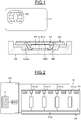
- the figure 1 represents an example of integrated circuit IC equipping a smart card CP.
- a typical CP smart card is schematically illustrated on the top of the figure 1 .
- the integrated circuit IC is assembled in the card body CB of the smart card CP, under MC contacts. A section of this assembly is shown on the bottom of the figure 1 .
- the integrated circuit IC conventionally comprises a semiconductor substrate surmounted by an interconnection portion (BEOL: Back End Of Lines).
- the integrated circuit IC is covered with an electrically conductive plate PC2.
- This plate is adhered to the rear face FR of said substrate by a conductive adhesive layer CA and attaches it to one face of a resin base RES.
- the RES resin base supports on its opposite face MC contacts dedicated to ensure the connections of the integrated circuit IC with a terminal such as a card reader.
- the integrated circuit IC is encapsulated in an Encap insulating encapsulation layer.
- the Encap insulating encapsulation layer is itself encapsulated in a CB card body.
- connections between the contacts MC and the integrated circuit IC are made by means of wires BW, in a typical flip chip configuration ("Flip chip” according to the usual English term), the BW wires being soldered on the one hand to said contacts MC and on the other hand contact pads ("pads" in English) formed on the last metallization level of the interconnection portion.
- BW flip chip
- the assembly formed by the electrically conductive plate PC2, the adhesive conductive layer CA and the resin RES form a coating of the integrated circuit IC.
- the figure 2 represents an exemplary embodiment of the integrated circuit IC.
- the integrated circuit IC comprises a semiconductor substrate having a front face FV, a rear face FR and contact points PCi, with i ⁇ ⁇ 10; 11; 12; 13 ⁇ , distributed at the front panel FV.
- the semiconductor substrate includes semiconductor casings CS electrically isolated from the rest of the substrate, for example by a structure of the triple well type ("triple well" according to the usual English term) conventional and known per se.
- the integrated circuit comprises a detection unit DIS connected to the electrically conductive plate PC2 and to the PCi contact points.
- the detection block DIS makes it possible to measure the resistive value of the substrate between contact points PCi, r being defined according to the type of measurement to be performed, and the electrically conductive plate PC2.
- the number r will take a value n during a first measurement, and will take another value m during a second measurement.
- the detection block DIS also makes it possible to perform a third measurement of the resistive value of the substrate between only PCi handshake.
- the detection block DIS comprises a measuring circuit MES configured to measure said resistive values of the substrate.
- the measuring circuit can deliver a physical quantity representative of the resistive value of the substrate, for example a voltage if a current of known value is circulated in the substrate between the contacts and the plate or else a current if a voltage of known value is applied between the contacts and the plate.
- the detection unit DIS further comprises two comparison circuits 10, 11 making it possible to compare the resistive value of the measured substrate with a nominal resistive value of the substrate.
- nominal resistive value the resistive value reasonably expected during a measurement performed on a structure that has not suffered damage to its integrity. Different nominal resistive values will respectively be associated with different measurements.
- the comparison circuits 10, 11 are described below, in connection with the Figures 6, 7 and 8 .
- the figure 3 represents the integrated circuit IC after undergoing an opening of the coating facing the rear face FR.
- the electrically conductive plate PC2 described above in connection with the Figures 1 and 2 has been removed, thus exposing the rear face FR of the substrate.
- the detection block DIS will make the first measurement of the resistive value R1 between n contact points corresponding to a measurement of the equivalent resistive value of n resistors connected in parallel, and a terminal normally connected to the electrically conductive plate. PC2.
- the removal of the electrically conductive plate PC2 leads to a sharp increase in the resistance of the substrate.
- the number n is advantageously chosen so that the nominal resistive value corresponding to the first measurement is sufficiently small to easily detect an increase in the measured resistive value.
- a removal of the electrically conductive plate PC2 leads to a very high measured resistive value.
- the resistive value R1 of the substrate resulting from the first measurement is then sent into the comparison circuit 10 configured to compare the resistive value R1 of the substrate resulting from the first measurement with a first nominal resistive value of the substrate REFH. If the resistive value R1 of the substrate resulting from the first measurement is greater than the first nominal resistive value REFH, the detection block has detected a withdrawal of at least a portion of said electrically conductive plate PC2.
- the figure 4 represents the integrated circuit IC after a thinning of the substrate and delivery of the electrically conductive plate PC2.
- Such thinning may comprise, for example, chemical-mechanical polishing from the rear face, and / or machining, for example via a FIB focused ion probe.
- the attacker can deposit an electrically conductive plate PC2 on the rear face FR.
- Thinning of the semiconductor substrate leads to a decrease in the resistive value of the substrate between PCi contact points and the electrically conductive plate PC2.
- the second measurement of the resistive value R2 of the substrate is made between m contact points corresponding to a measurement of the equivalent resistive value of m resistors connected in parallel, and the electrically conductive plate PC2.
- a nominal resistive value according to this measurement thus decreases in 1 / m.
- the second measurement is similar to the first measurement, except that the number m is advantageously chosen so that the corresponding nominal resistive value is sufficiently large to easily detect a decrease in the measured resistive value.
- the geometric distribution of the contact m on the front face of the substrate is advantageously chosen to perform such a measurement.
- the measurement may be performed globally in the substrate, or sequentially in local regions of the substrate.
- the resistive value R2 of the substrate resulting from the second measurement is sent in a comparison circuit 11 configured to compare the resistive value R2 of the substrate resulting from the second measurement with a second nominal resistive value of the substrate REFB. If the resistive value R2 of the substrate resulting from the second measurement is lower than said second nominal resistive value REFB, a thinning of the substrate is detected by the detection block.
- the figure 5 schematically illustrates the integrated circuit IC after several thinning operations a1 and a2 respectively leading to substrate thicknesses d1 and d2.
- the thinning operation reaches, at least over a portion of the substrate, a region of insulation such as the bottom of a box CS or even a region of lateral insulation of the trench type of shallow insulation STI ("Shallow Trench Isolation"), or local oxide (LOCOS for "LOCal Oxidation of Silicon” according to the Usual term Anglosaxon).
- a region of insulation such as the bottom of a box CS or even a region of lateral insulation of the trench type of shallow insulation STI ("Shallow Trench Isolation"), or local oxide (LOCOS for "LOCal Oxidation of Silicon” according to the Usual term Anglosaxon).
- two contacts can be electrically isolated from each other, or connected by a resistive path via the remainder of the substrate longer than in an unaltered configuration, and then the resistive value R3 of the substrate output the third measurement between handsets PCi increases sharply. This corresponds by abuse of language to an open circuit.
- the resistive value R3 resulting from the third measurement is sent in the comparison circuits 10 and 11 in the two cases of damage to the integrity of the substrate, that is to say, the realization of an open-circuit or a short circuit.
- the comparison circuit 10 If the resistive value R3 of the substrate resulting from the third measurement is greater than a corresponding nominal resistive value of said substrate REFH2, the comparison circuit 10 generates an alarm signal.
- the comparison circuit 11 If the resistive value R3 of the substrate resulting from the third measurement is lower than another nominal resistive value corresponding to said substrate REFB2, the comparison circuit 11 generates an alarm signal.
- the figure 6 schematically illustrates the first comparison circuit 10 for implementing the first detection of a breach of the integrity of the substrate in relation to the first measurement, described above in connection with the figure 3 .
- the measured resistive value R1 is sent to a non-inverting input of a comparator COM1.
- An inverting input takes as input a first resistive nominal value REFH of the substrate.
- the comparator COM1 compares the two received input values on its two terminals and generates an ALR alarm signal if the resistive value R1 resulting from the first measurement is greater than the first nominal resistive value REFH of the substrate.
- the alarm signal ALR will be generated.
- the ALR alarm signal makes it possible, for example, to trigger conventional means of countermeasures for counteracting the attack on the substrate.
- the figure 7 schematically illustrates the second comparison circuit 11 to implement the second detection of a breach of the integrity of the substrate in relation to the second measurement, described above in connection with the figure 4 .
- the measured resistive value R2 resulting from the second measurement is sent to an inverting input of a comparator COM2.
- a non-inverting input takes as input a second nominal resistive value REFB of the substrate.
- the comparator COM2 compares the two received input values on its two terminals and generates an alarm signal ALR if the resistive value R2 resulting from the second measurement is lower than the nominal resistive value REFB of the substrate.
- the ALR alarm signal will be generated.
- the alarm signal ALR makes it possible, for example, to trigger conventional means of countermeasures intended to counteract the attack made on the substrate.
- the figure 8 schematically illustrates the two comparison blocks 10 and 11 relative to the third measurement.
- the measured resistive value R3 is sent to the non-inverting first comparator input COM1, and to the inverting input of a second comparator COM2.
- comparator COM1 receives a third nominal resistive value REFH2 of the substrate.
- the non-inverting input of the second comparator COM2 receives another third nominal resistive value REFB of the substrate.
- the first comparator COM1 compares the two received input values on its two terminals and generates an alarm signal ALR if the resistive value R3 resulting from the third measurement is greater than the nominal resistive value REFH2 of the substrate.
- the alarm signal ALR will be generated.
- the second comparator COM2 compares the two received input values on its two terminals and generates an alarm signal ALR if the resistive value R3 resulting from the third measurement is lower than the nominal resistive value REFB2 of the substrate.
- the alarm signal ALR is generated.
- the alarm signal ALR makes it possible, for example, to trigger conventional means of countermeasures intended to counteract the attack made on the substrate.
- the invention is not limited to these embodiments but embraces all variants, for example undescribed combinations of contact points can be used to implement the first, second or third measurements, and that the use of known means not described to implement said measures.
Landscapes
- Engineering & Computer Science (AREA)
- Computer Hardware Design (AREA)
- Physics & Mathematics (AREA)
- General Physics & Mathematics (AREA)
- Microelectronics & Electronic Packaging (AREA)
- Theoretical Computer Science (AREA)
- General Engineering & Computer Science (AREA)
- Computer Security & Cryptography (AREA)
- Condensed Matter Physics & Semiconductors (AREA)
- Power Engineering (AREA)
- Mathematical Physics (AREA)
- Software Systems (AREA)
- Environmental & Geological Engineering (AREA)
- Testing Or Measuring Of Semiconductors Or The Like (AREA)
- Semiconductor Integrated Circuits (AREA)
Applications Claiming Priority (1)
| Application Number | Priority Date | Filing Date | Title |
|---|---|---|---|
| FR1851011A FR3077678B1 (fr) | 2018-02-07 | 2018-02-07 | Procede de detection d'une atteinte a l'integrite d'un substrat semi-conducteur d'un circuit integre depuis sa face arriere, et dispositif correspondant |
Publications (1)
| Publication Number | Publication Date |
|---|---|
| EP3525236A1 true EP3525236A1 (de) | 2019-08-14 |
Family
ID=62597605
Family Applications (1)
| Application Number | Title | Priority Date | Filing Date |
|---|---|---|---|
| EP19153676.2A Pending EP3525236A1 (de) | 2018-02-07 | 2019-01-25 | Verfahren zur erfassung einer beeinträchtigung der integrität eines halbleitersubstrats eines integrierten schaltkreises von seiner rückseite aus, und entsprechende vorrichtung |
Country Status (4)
| Country | Link |
|---|---|
| US (1) | US11270957B2 (de) |
| EP (1) | EP3525236A1 (de) |
| CN (2) | CN209542789U (de) |
| FR (1) | FR3077678B1 (de) |
Families Citing this family (2)
| Publication number | Priority date | Publication date | Assignee | Title |
|---|---|---|---|---|
| FR3077678B1 (fr) | 2018-02-07 | 2022-10-21 | St Microelectronics Rousset | Procede de detection d'une atteinte a l'integrite d'un substrat semi-conducteur d'un circuit integre depuis sa face arriere, et dispositif correspondant |
| FR3096175B1 (fr) | 2019-05-13 | 2021-05-07 | St Microelectronics Rousset | Procédé de détection d’une atteinte éventuelle à l’intégrité d’un substrat semi-conducteur d’un circuit intégré depuis sa face arrière, et circuit intégré correspondant |
Citations (4)
| Publication number | Priority date | Publication date | Assignee | Title |
|---|---|---|---|---|
| WO2009016589A2 (en) * | 2007-08-02 | 2009-02-05 | Nxp B.V. | Tamper-resistant semiconductor device and methods of manufacturing thereof |
| FR2986356A1 (fr) * | 2012-01-27 | 2013-08-02 | St Microelectronics Rousset | Dispositif de protection d'un circuit integre contre des attaques en face arriere |
| FR2998419A1 (fr) * | 2012-11-21 | 2014-05-23 | St Microelectronics Rousset | Protection d'un circuit integre contre des attaques |
| US20160042199A1 (en) * | 2014-08-06 | 2016-02-11 | Maxim Integrated Products, Inc. | Detecting and thwarting backside attacks on secured systems |
Family Cites Families (23)
| Publication number | Priority date | Publication date | Assignee | Title |
|---|---|---|---|---|
| US7102522B2 (en) * | 2002-12-24 | 2006-09-05 | 3M Innovative Properties Company | Tamper-indicating radio frequency identification antenna and sticker, a radio frequency identification antenna, and methods of using the same |
| TWI286372B (en) * | 2003-08-13 | 2007-09-01 | Phoenix Prec Technology Corp | Semiconductor package substrate with protective metal layer on pads formed thereon and method for fabricating the same |
| JP2005303099A (ja) | 2004-04-14 | 2005-10-27 | Hitachi High-Technologies Corp | プラズマ処理装置およびプラズマ処理方法 |
| CN101382581A (zh) * | 2004-09-02 | 2009-03-11 | 松下电器产业株式会社 | 半导体集成电路器件及其检测方法、半导体晶片、以及老化检测设备 |
| US7323986B2 (en) * | 2004-09-03 | 2008-01-29 | Gore Enterprise Holdings, Inc. | Reusable tamper respondent enclosure |
| FR2887076B1 (fr) | 2005-06-10 | 2007-08-31 | Atmel Grenoble Soc Par Actions | Capteur d'image a substrat semiconducteur aminci avec metallisation arriere |
| KR100663364B1 (ko) * | 2005-07-12 | 2007-01-02 | 삼성전자주식회사 | 퓨즈 분리 장벽을 갖는 퓨즈 영역을 구비하는 반도체소자및 그 제조방법들 |
| US7473979B2 (en) | 2006-05-30 | 2009-01-06 | International Business Machines Corporation | Semiconductor integrated circuit devices having high-Q wafer back-side capacitors |
| US8522051B2 (en) * | 2007-05-07 | 2013-08-27 | Infineon Technologies Ag | Protection for circuit boards |
| FR2946775A1 (fr) * | 2009-06-15 | 2010-12-17 | St Microelectronics Rousset | Dispositif de detection d'amincissement du substrat d'une puce de circuit integre |
| US20110210956A1 (en) | 2010-02-26 | 2011-09-01 | Dev Alok Girdhar | Current sensor for a semiconductor device and system |
| CN101819941B (zh) * | 2010-04-29 | 2014-03-12 | 上海宏力半导体制造有限公司 | 半导体器件栅氧化层完整性的测试结构 |
| CN102157363B (zh) | 2011-03-08 | 2012-06-27 | 电子科技大学 | 一种功率器件衬底背面的离子注入方法 |
| US9159209B2 (en) * | 2013-03-15 | 2015-10-13 | Ut-Battelle, Llc | Conductive fabric seal |
| US9431354B2 (en) * | 2014-11-06 | 2016-08-30 | International Business Machines Corporation | Activating reactions in integrated circuits through electrical discharge |
| FR3041814A1 (fr) * | 2015-09-30 | 2017-03-31 | Stmicroelectronics Rousset | Circuit integre securise |
| FR3048103B1 (fr) | 2016-02-22 | 2018-03-23 | Stmicroelectronics (Rousset) Sas | Procede de detection d'un amincissement du substrat semi-conducteur d'un circuit integre depuis sa face arriere et circuit integre correspondant |
| US10651135B2 (en) * | 2016-06-28 | 2020-05-12 | Marvell Asia Pte, Ltd. | Tamper detection for a chip package |
| FR3063385B1 (fr) | 2017-02-28 | 2019-04-26 | Stmicroelectronics (Rousset) Sas | Circuit integre avec detection d'amincissement par la face arriere et condensateurs de decouplage |
| FR3069954B1 (fr) | 2017-08-01 | 2020-02-07 | Stmicroelectronics (Rousset) Sas | Procede de detection d'un amincissement du substrat d'un circuit integre par sa face arriere, et circuit integre associe |
| FR3071100B1 (fr) | 2017-09-13 | 2021-12-10 | St Microelectronics Rousset | Procede de detection d'un amincissement d'un substrat de circuit integre par sa face arriere, et circuit integre correspondant |
| FR3072211B1 (fr) | 2017-10-11 | 2021-12-10 | St Microelectronics Rousset | Procede de detection d'une injection de fautes et d'un amincissement du substrat dans un circuit integre, et circuit integre associe |
| FR3077678B1 (fr) | 2018-02-07 | 2022-10-21 | St Microelectronics Rousset | Procede de detection d'une atteinte a l'integrite d'un substrat semi-conducteur d'un circuit integre depuis sa face arriere, et dispositif correspondant |
-
2018
- 2018-02-07 FR FR1851011A patent/FR3077678B1/fr active Active
-
2019
- 2019-01-25 CN CN201920133627.2U patent/CN209542789U/zh not_active Withdrawn - After Issue
- 2019-01-25 CN CN201910075225.6A patent/CN110118924B/zh active Active
- 2019-01-25 EP EP19153676.2A patent/EP3525236A1/de active Pending
- 2019-02-05 US US16/267,573 patent/US11270957B2/en active Active
Patent Citations (4)
| Publication number | Priority date | Publication date | Assignee | Title |
|---|---|---|---|---|
| WO2009016589A2 (en) * | 2007-08-02 | 2009-02-05 | Nxp B.V. | Tamper-resistant semiconductor device and methods of manufacturing thereof |
| FR2986356A1 (fr) * | 2012-01-27 | 2013-08-02 | St Microelectronics Rousset | Dispositif de protection d'un circuit integre contre des attaques en face arriere |
| FR2998419A1 (fr) * | 2012-11-21 | 2014-05-23 | St Microelectronics Rousset | Protection d'un circuit integre contre des attaques |
| US20160042199A1 (en) * | 2014-08-06 | 2016-02-11 | Maxim Integrated Products, Inc. | Detecting and thwarting backside attacks on secured systems |
Also Published As
| Publication number | Publication date |
|---|---|
| CN110118924B (zh) | 2022-04-29 |
| US20190244915A1 (en) | 2019-08-08 |
| FR3077678A1 (fr) | 2019-08-09 |
| CN209542789U (zh) | 2019-10-25 |
| US11270957B2 (en) | 2022-03-08 |
| FR3077678B1 (fr) | 2022-10-21 |
| CN110118924A (zh) | 2019-08-13 |
Similar Documents
| Publication | Publication Date | Title |
|---|---|---|
| EP2232412B1 (de) | Manipulationssicheres halbleiterbauelement und verfahren zu seiner herstellung | |
| EP2369622B1 (de) | Verfahren und Vorrichtung für Gegenmassnahme gegenüber einem Angriff durch Fehlerinjektion in einem elektronischen Mikroschaltungskarte | |
| FR3063385A1 (fr) | Circuit integre avec detection d'amincissement par la face arriere et condensateurs de decouplage | |
| EP3605543B1 (de) | Detektionsverfahren eines angriffs durch einen elektrisch geladenen teilchenstrahl auf einen integrierten schaltkreis, und entsprechender integrierter schaltkreis | |
| FR2697673A1 (fr) | Circuit à fusible, pour circuit intégré. | |
| EP3291293B1 (de) | Chip, der gegen angriffe auf die rückseite geschützt ist | |
| EP3525236A1 (de) | Verfahren zur erfassung einer beeinträchtigung der integrität eines halbleitersubstrats eines integrierten schaltkreises von seiner rückseite aus, und entsprechende vorrichtung | |
| EP2432302B1 (de) | Schutzvorrichtung für einen gedruckten elektronischen Schaltkreis | |
| EP3301605B1 (de) | Geschützter elektronischer chip | |
| EP0905776A1 (de) | Halbleiteranordnung mit zwei mit einem Erdungsanschluss verbundenen Erdungsverbindungspunkten und Testverfahren dafür | |
| FR3071100A1 (fr) | Procede de detection d'un amincissement d'un substrat de circuit integre par sa face arriere, et circuit integre correspondant | |
| FR3072211A1 (fr) | Procede de detection d'une injection de fautes et d'un amincissement du substrat dans un circuit integre, et circuit integre associe | |
| FR3112004A1 (fr) | Détection d'une impulsion électromagnétique | |
| EP2076925B1 (de) | Einrichtung zum elektromagnetischen koppeln eines elektromagnetischen strahlungssensors | |
| EP3739622A1 (de) | Verfahren zur erfassung der möglichen verletzung der integrität eines halbleitersubstrats eines integrierten schaltkreises von seiner rückseite aus, und entsprechender integrierter schaltkreis | |
| FR3074605A1 (fr) | Procede de detection d'un amincissement eventuel d'un substrat d'un circuit integre par sa face arriere, et dispositif associe | |
| EP1400887A1 (de) | Schutzgerät für einen elektronischen Chip, der vertaulichen Informationen enthält | |
| FR2801999A1 (fr) | Procede de protection physique de puces electroniques et dispositifs electroniques ainsi proteges | |
| EP1733428A1 (de) | Durch aktive abschirmung geschützte integrierte schaltung | |
| FR3084520A1 (fr) | Procede de protection d'un circuit integre, et dispositif correspondant | |
| FR3085540A1 (fr) | Dispositif integre de mesure temporelle a constante de temps ultra longue et procede de fabrication | |
| FR3084521A1 (fr) | Procede de protection d'un module de circuit integre et dispositif correspondant | |
| US7291508B2 (en) | Laser probe points | |
| FR3071101A1 (fr) | Empilement de puces | |
| EP1372237B1 (de) | Elektrisches Gerät mit zwei Unterlagen und Anschlussklemme verbunden mit einem Reihenkodensator und Spannungsbegrenzer |
Legal Events
| Date | Code | Title | Description |
|---|---|---|---|
| PUAI | Public reference made under article 153(3) epc to a published international application that has entered the european phase |
Free format text: ORIGINAL CODE: 0009012 |
|
| STAA | Information on the status of an ep patent application or granted ep patent |
Free format text: STATUS: REQUEST FOR EXAMINATION WAS MADE |
|
| 17P | Request for examination filed |
Effective date: 20190125 |
|
| AK | Designated contracting states |
Kind code of ref document: A1 Designated state(s): AL AT BE BG CH CY CZ DE DK EE ES FI FR GB GR HR HU IE IS IT LI LT LU LV MC MK MT NL NO PL PT RO RS SE SI SK SM TR |
|
| AX | Request for extension of the european patent |
Extension state: BA ME |
|
| STAA | Information on the status of an ep patent application or granted ep patent |
Free format text: STATUS: EXAMINATION IS IN PROGRESS |
|
| 17Q | First examination report despatched |
Effective date: 20220511 |