EP3518518B1 - Imaging device and electronic apparatus - Google Patents
Imaging device and electronic apparatus Download PDFInfo
- Publication number
- EP3518518B1 EP3518518B1 EP19154945.0A EP19154945A EP3518518B1 EP 3518518 B1 EP3518518 B1 EP 3518518B1 EP 19154945 A EP19154945 A EP 19154945A EP 3518518 B1 EP3518518 B1 EP 3518518B1
- Authority
- EP
- European Patent Office
- Prior art keywords
- imaging device
- group
- transistor
- pixel
- solid
- Prior art date
- Legal status (The legal status is an assumption and is not a legal conclusion. Google has not performed a legal analysis and makes no representation as to the accuracy of the status listed.)
- Active
Links
- 238000003384 imaging method Methods 0.000 title claims description 118
- 230000003321 amplification Effects 0.000 claims description 72
- 238000003199 nucleic acid amplification method Methods 0.000 claims description 72
- 238000006243 chemical reaction Methods 0.000 claims description 26
- 238000009792 diffusion process Methods 0.000 claims description 5
- 239000011159 matrix material Substances 0.000 claims 15
- 238000012546 transfer Methods 0.000 description 56
- 238000005516 engineering process Methods 0.000 description 37
- 238000012545 processing Methods 0.000 description 34
- 238000010586 diagram Methods 0.000 description 22
- 229910021420 polycrystalline silicon Inorganic materials 0.000 description 15
- 229920005591 polysilicon Polymers 0.000 description 15
- 230000000694 effects Effects 0.000 description 10
- 238000005286 illumination Methods 0.000 description 9
- 230000003287 optical effect Effects 0.000 description 5
- 230000000875 corresponding effect Effects 0.000 description 4
- 238000002955 isolation Methods 0.000 description 3
- 230000004075 alteration Effects 0.000 description 2
- 230000015556 catabolic process Effects 0.000 description 2
- 238000001459 lithography Methods 0.000 description 2
- 238000012986 modification Methods 0.000 description 2
- 230000004048 modification Effects 0.000 description 2
- 230000002093 peripheral effect Effects 0.000 description 2
- 230000004044 response Effects 0.000 description 2
- 239000004065 semiconductor Substances 0.000 description 2
- 230000035945 sensitivity Effects 0.000 description 2
- 239000000758 substrate Substances 0.000 description 2
- XUIMIQQOPSSXEZ-UHFFFAOYSA-N Silicon Chemical compound [Si] XUIMIQQOPSSXEZ-UHFFFAOYSA-N 0.000 description 1
- 238000010521 absorption reaction Methods 0.000 description 1
- 238000009825 accumulation Methods 0.000 description 1
- 230000002730 additional effect Effects 0.000 description 1
- 230000003139 buffering effect Effects 0.000 description 1
- 230000008859 change Effects 0.000 description 1
- 230000000295 complement effect Effects 0.000 description 1
- 238000012937 correction Methods 0.000 description 1
- 230000002596 correlated effect Effects 0.000 description 1
- 230000003247 decreasing effect Effects 0.000 description 1
- 230000001419 dependent effect Effects 0.000 description 1
- 230000006870 function Effects 0.000 description 1
- 230000006872 improvement Effects 0.000 description 1
- 229910044991 metal oxide Inorganic materials 0.000 description 1
- 150000004706 metal oxides Chemical class 0.000 description 1
- 238000000034 method Methods 0.000 description 1
- 230000008569 process Effects 0.000 description 1
- 238000005070 sampling Methods 0.000 description 1
- 229910052710 silicon Inorganic materials 0.000 description 1
- 239000010703 silicon Substances 0.000 description 1
Images


Classifications
-
- H—ELECTRICITY
- H01—ELECTRIC ELEMENTS
- H01L—SEMICONDUCTOR DEVICES NOT COVERED BY CLASS H10
- H01L27/00—Devices consisting of a plurality of semiconductor or other solid-state components formed in or on a common substrate
- H01L27/14—Devices consisting of a plurality of semiconductor or other solid-state components formed in or on a common substrate including semiconductor components sensitive to infrared radiation, light, electromagnetic radiation of shorter wavelength or corpuscular radiation and specially adapted either for the conversion of the energy of such radiation into electrical energy or for the control of electrical energy by such radiation
- H01L27/144—Devices controlled by radiation
- H01L27/146—Imager structures
- H01L27/14601—Structural or functional details thereof
- H01L27/14603—Special geometry or disposition of pixel-elements, address-lines or gate-electrodes
-
- H—ELECTRICITY
- H01—ELECTRIC ELEMENTS
- H01L—SEMICONDUCTOR DEVICES NOT COVERED BY CLASS H10
- H01L27/00—Devices consisting of a plurality of semiconductor or other solid-state components formed in or on a common substrate
- H01L27/14—Devices consisting of a plurality of semiconductor or other solid-state components formed in or on a common substrate including semiconductor components sensitive to infrared radiation, light, electromagnetic radiation of shorter wavelength or corpuscular radiation and specially adapted either for the conversion of the energy of such radiation into electrical energy or for the control of electrical energy by such radiation
- H01L27/144—Devices controlled by radiation
- H01L27/146—Imager structures
- H01L27/14643—Photodiode arrays; MOS imagers
-
- H—ELECTRICITY
- H04—ELECTRIC COMMUNICATION TECHNIQUE
- H04N—PICTORIAL COMMUNICATION, e.g. TELEVISION
- H04N25/00—Circuitry of solid-state image sensors [SSIS]; Control thereof
- H04N25/60—Noise processing, e.g. detecting, correcting, reducing or removing noise
-
- H—ELECTRICITY
- H01—ELECTRIC ELEMENTS
- H01L—SEMICONDUCTOR DEVICES NOT COVERED BY CLASS H10
- H01L27/00—Devices consisting of a plurality of semiconductor or other solid-state components formed in or on a common substrate
- H01L27/14—Devices consisting of a plurality of semiconductor or other solid-state components formed in or on a common substrate including semiconductor components sensitive to infrared radiation, light, electromagnetic radiation of shorter wavelength or corpuscular radiation and specially adapted either for the conversion of the energy of such radiation into electrical energy or for the control of electrical energy by such radiation
- H01L27/144—Devices controlled by radiation
- H01L27/146—Imager structures
- H01L27/14601—Structural or functional details thereof
- H01L27/14609—Pixel-elements with integrated switching, control, storage or amplification elements
-
- H—ELECTRICITY
- H01—ELECTRIC ELEMENTS
- H01L—SEMICONDUCTOR DEVICES NOT COVERED BY CLASS H10
- H01L27/00—Devices consisting of a plurality of semiconductor or other solid-state components formed in or on a common substrate
- H01L27/14—Devices consisting of a plurality of semiconductor or other solid-state components formed in or on a common substrate including semiconductor components sensitive to infrared radiation, light, electromagnetic radiation of shorter wavelength or corpuscular radiation and specially adapted either for the conversion of the energy of such radiation into electrical energy or for the control of electrical energy by such radiation
- H01L27/144—Devices controlled by radiation
- H01L27/146—Imager structures
- H01L27/14601—Structural or functional details thereof
- H01L27/14641—Electronic components shared by two or more pixel-elements, e.g. one amplifier shared by two pixel elements
-
- H—ELECTRICITY
- H04—ELECTRIC COMMUNICATION TECHNIQUE
- H04N—PICTORIAL COMMUNICATION, e.g. TELEVISION
- H04N25/00—Circuitry of solid-state image sensors [SSIS]; Control thereof
- H04N25/70—SSIS architectures; Circuits associated therewith
- H04N25/76—Addressed sensors, e.g. MOS or CMOS sensors
- H04N25/77—Pixel circuitry, e.g. memories, A/D converters, pixel amplifiers, shared circuits or shared components
- H04N25/778—Pixel circuitry, e.g. memories, A/D converters, pixel amplifiers, shared circuits or shared components comprising amplifiers shared between a plurality of pixels, i.e. at least one part of the amplifier must be on the sensor array itself
-
- H—ELECTRICITY
- H04—ELECTRIC COMMUNICATION TECHNIQUE
- H04N—PICTORIAL COMMUNICATION, e.g. TELEVISION
- H04N25/00—Circuitry of solid-state image sensors [SSIS]; Control thereof
- H04N25/70—SSIS architectures; Circuits associated therewith
- H04N25/71—Charge-coupled device [CCD] sensors; Charge-transfer registers specially adapted for CCD sensors
- H04N25/75—Circuitry for providing, modifying or processing image signals from the pixel array
Definitions
- the present disclosure relates to an imaging device and an electronic apparatus, particularly the solid-state imaging device and the electronic apparatus in which random noise can be improved.
- CMOS image sensor In a backside illumination type CMOS image sensor disclosed in JP 2013-62789A , which adopts a pixel sharing layout as a countermeasure against PRNU (photo response non uniformity: sensitivity ununiformity), pixel transistors (hereinafter, referred to as pixel Tr.) are divided into two groups, and Trs. are symmetrically arranged.
- PRNU photo response non uniformity: sensitivity ununiformity
- This technology is directed to equalize an amount of reflection or absorption of incident light from the back surface side by polysilicon of the transistors (Trs.) between the two groups by symmetrically arranging an amplification Tr. (hereinafter referred to as AMP), a selection Tr. (hereinafter referred to as SEL), and a reset Tr. (hereinafter referred to as RST) with respect to a photodiode (hereinafter referred to as PD).
- AMP an amplification Tr.
- SEL selection Tr.
- RST reset Tr.
- EP 2 563 011 A2 relates to a solid-state imaging device including shared pixel unit parts including 2, 4 or 8 photodiodes and shared transistors.
- the required number of source-drain is three in the group 1 and three in the group 2, that is, in total six.
- there is a limit in elongating the L-length of the Tr. because of limitation in a lithography line width, limitation in processing the polysilicon and a contact hole, securing isolation breakdown voltage, and so on.
- the influence from such a state is quite serious, and RN margin may deteriorate due to the short L-length of the AMP.
- the present disclosure is achieved in consideration of the above-described situation, and random noise margin can be improved by the present disclosure.
- the invention provides an imaging device in accordance with claim 1.
- the invention provides an electronic apparatus in accordance with claim 10. Further aspects of the invention are set forth the dependent claims, the drawings and the following description of embodiments.
- a solid-state imaging device includes: a photoelectric conversion element group including a sharing unit shaped in a rectangle; and a pixel transistor group arranged as one group in long side direction of the photoelectric conversion element group, wherein respective pixel transistors of the pixel transistor group are arranged so as to be substantially symmetric with respect to the photoelectric conversion element group.
- a dummy transistor is included in the pixel transistor group.
- the pixel transistor group is arranged at a position shifted from the rectangular shaped sharing unit of the photoelectric conversion element group.
- An L-length of an amplification transistor included in the pixel transistor group is longer than L-lengths of other transistors included in the pixel transistor group.
- the L-length of the amplification transistor included in the pixel transistor group is 0.6 to 1.4 times of a pitch of the photoelectric conversion element group.
- An L-length of a selection transistor included in the pixel transistor group is longer than L-lengths of other transistors included in the pixel transistor group.
- a well contact is further provided between the photoelectric conversion element group and another photoelectric conversion element group positioned next to the photoelectric conversion element group.
- a well contact is further provided between the pixel transistor group and another pixel transistor group positioned next to the pixel transistor group.
- the solid-state imaging device is a backside illumination type.
- a dummy transistor is included in the pixel transistor group.
- the pixel transistor group is arranged at a position shifted from the rectangular shaped sharing unit of the photoelectric conversion element group.
- An L-length of an amplification transistor included in the pixel transistor group is longer than L-lengths of other transistors included in the pixel transistor group.
- the L-length of the amplification transistor included in the pixel transistor group is 0.6 to 1.4 times of a pitch of the photoelectric conversion element group.
- a well contact is further provided between the photoelectric conversion element group and another photoelectric conversion element group positioned next to the photoelectric conversion element group.
- a well contact is further provided between the pixel transistor group and another pixel transistor group positioned next to the pixel transistor group.
- the solid-state imaging device is a backside illumination type.
- a photoelectric conversion element group includes a sharing unit shaped in a rectangle, and a pixel transistor group is arranged, as a group, in a direction of a long side of the photoelectric conversion element group. Further, respective pixel transistors of the pixel transistor group are arranged so as to be substantially symmetric with respect to the photoelectric conversion element group.
- polysilicon forming the transistors can be arranged substantially symmetrically with respect to the photodiodes. Further, according to an embodiment of the present technology, random noise can be decreased.
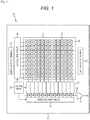
- Fig. 1 is a diagram illustrating an example of a schematic configuration of a CMOS (Complementary Metal Oxide Semiconductor) solid-state imaging device applied to respective embodiments of the present technology.
- CMOS Complementary Metal Oxide Semiconductor
- a solid-state imaging device (device chip) 1 includes a pixel area (so-called imaging area) 3 and a peripheral circuit.
- pixel area 3 pixels 2 including a plurality of photoelectric conversion elements are regularly and two-dimensionally arrayed on a semiconductor substrate 11 (e.g., silicon substrate).
- the pixel 2 includes a photoelectric conversion element (e.g., photodiode) and a plurality of pixel transistors (so-called MOS transistors).
- the plurality of pixel transistors may include three transistors such as a transfer transistor, a reset transistor, and an amplification transistor, and also may include four transistors by further adding a selection transistor.
- An equivalent circuit of each pixel 2 (unit pixel) is same as those generally applied, and therefore a description therefor will be omitted here.
- the pixel 2 may have a structure of pixel sharing.
- the structure of pixel sharing includes a plurality of photodiodes, a plurality of transfer transistors, one floating diffusion to be shared, and one in each of other pixel transistors to be shared.
- the photodiode is a photoelectric conversion element.
- a peripheral circuit includes a vertical drive circuit 4, a column signal processing circuit 5, a horizontal drive circuit 6, an output circuit 7, and a control circuit 8.
- the control circuit 8 receives data to execute commands for an input clock, an operation mode, etc., and outputs data such as internal information of the solid-state imaging device 1. More specifically, the control circuit 8 generates a vertical synchronizing signal and a horizontal synchronizing signal and also generates, based on a master clock, a clock signal and a control signal which controls operation of the vertical drive circuit 4, column signal processing circuit 5, and horizontal drive circuit 6. Further, the control circuit 8 inputs these signals to the vertical drive circuit 4, column signal processing circuit 5, and horizontal drive circuit 6.
- the vertical drive circuit 4 includes, for example, a shift register, and selects a pixel driving wire, supplies the selected pixel driving wire with a pulse to drive the pixel 2, and drives the pixel 2 in units of rows. More specifically, the vertical drive circuit 4 selectively scans each one of the pixels 2 in a pixel area 3 sequentially in a vertical direction in units of rows, and supplies, via a vertical signal line 9, the column signal processing circuit 5 with a pixel signal based on signal charge generated in accordance with a light receiving amount in the photoelectric conversion element in each of the pixels 2.
- the column signal processing circuit 5 is arranged, for example, per column of the pixels 2 and executes, in units of columns of the pixels, signal processing such as noise removal for a signal output from the pixels 2 of one row. More specifically, the column signal processing circuit 5 executes the signal processing such as CDS (Correlated Double Sampling), signal amplification, A/D (Analog/Digital) conversion, etc. in order to remove fixed pattern noise unique to the pixel 2.
- a horizontal selection switch (not illustrated) is provided at an output stage of the column signal processing circuit 5, being connected on the way to the horizontal signal line 10.
- the horizontal drive circuit 6 includes, for example, the shift register, and sequentially outputs a horizontal scan pulse, thereby selecting each one of the column signal processing circuits 5 in order, and causing each one of the column signal processing circuits 5 to output the pixel signal to the horizontal signal line 10.
- the output circuit 7 executes signal processing for the signal sequentially supplied from each one of the column signal processing circuits 5 via the horizontal signal line 10 and outputs the signal.
- the output circuit 7 may execute, for example, only buffering, or may execute black level adjustment, column variation correction, various kinds of digital signal processing, and so on.
- An input and output terminal 12 is provided to exchange signals with components or devices.
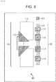
- Fig. 2 is a diagram illustrating an exemplary configuration of a pixel in a global shutter type CMOS sensor.
- the exemplary configuration including three transistors hereinafter referred to as Tr.
- Tr. three transistors
- 3-Tr. type 3-Tr. type
- the pixel 2 in Fig. 2 includes one floating diffusion to be shared (hereinafter referred to as FD) 21, a photodiode 22, and three shared or pixel transistors inside a unit pixel.
- the three shared Trs. are a reset Tr. 23, a transfer Tr. 24, and an amplification Tr. 25 respectively.
- the photodiode 22 has an anode electrode connected to a negative side power source (e.g., ground), and photoelectrically converts received light to photo-charge (photoelectron, in this case) in accordance with a light amount.
- the photodiode 22 has a cathode electrode electrically connected to a gate electrode of the amplification Tr. 25 via a transfer Tr. 24.
- a node electrically connected to the gate electrode of the amplification Tr. 25 and the transfer Tr. 24 is the FD 21.
- the transfer Tr. 24 is connected between the cathode electrode of the photodiode 22 and the FD 21.
- a transfer pulse ⁇ TRF having an active high level (e.g., VDD level) (hereinafter referred to as high active) is received by the gate electrode of the transfer Tr. 24 via a transfer line not illustrated.
- the transfer Tr. 24 becomes an ON state, and transfers the photo-charge which has been photoelectrically converted at the photodiode 22 to the FD 21.
- the reset Tr. 23 has a drain electrode connected to the pixel power source VDD, and a source electrode connected to the FD 21 respectively.
- a high active reset pulse ⁇ RST is received by a gate electrode of the reset Tr. 23 via a reset line (not illustrated) before transference of signal charge from the photodiode 22 to the FD 21.
- the reset Tr. 23 is placed in an ON state, and discharges the electric charge of the FD 21 to the pixel power source VDD, thereby resetting the FD 21.
- the amplification Tr. 25 has a gate electrode connected to the FD 21, a drain electrode connected to the pixel power source VDD, and a source electrode connected to the vertical signal line. Also, the amplification Tr. 25 outputs, as a reset signal (reset level) Vreset, a potential of the FD 21 which has been reset by the reset Tr. 23. Further, the amplification Tr. 25 further outputs, as a light accumulation signal (signal level) Vsig, the potential of the FD 21 after the signal charged is transferred by the transfer Tr. 24.
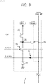
- Fig. 3 is a diagram illustrating a different configuration of the pixel in the global shutter type CMOS sensor.
- the exemplary configuration of four Trs. hereinafter also referred to as 4-Tr. type is illustrated.
- a pixel 2 in Fig. 3 is similar to the pixel 2 in Fig 2 in that both pixels 2 include the FD 21, photodiode 22, reset Tr. 23, transfer Tr. 24, and amplification Tr. 25.
- the pixel 2 in Fig. 3 differs from the pixel 2 in Fig. 2 that a selection Tr. 31 is added.
- the selection Tr. 31 has a drain electrode connected to a source electrode of the amplification Tr. 25, and a source electrode connected to the vertical signal line respectively, for example.
- a high active selection pulse ⁇ SEL is received by the gate electrode of the selection Tr. 31 via a selection line not illustrated.
- the selection Tr. 31 enters an ON state and places a unit pixel in a selected state, thereby relaying a signal output from the amplification Tr. 25 to the vertical signal line.
- the selection Tr. 31 may be connected between the pixel power source VDD and the drain of the amplification Tr. 25 as well.
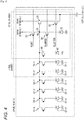
- Fig. 4 is a diagram illustrating a structure where one set of Trs. is shared by two pixels, four pixels, and eight pixels.
- the set of Trs. includes the reset Tr. 23 and amplification Tr. 25 described above with reference to Fig. 2 , or the reset Tr. 23, amplification Tr. 25, and selection Tr. 31 described with reference to Fig. 3 .
- a transfer Tr. is required for each photodiode, and is directly connected to each photodiode.
- a pair of the transfer Tr. 41 and the photodiode 42 is added to the configuration of the pixel 2 in Fig. 3 via the FD 21.
- one set of Trs. is configured to be shared by the two pixels (photodiode 22 and photodiode 42).
- Trs. 51-1, 51-2 and photodiodes 52-1, 52-2 are further added to the above-described 2-pixel sharing structure via the FD 21.
- one set of Trs. is configured to be shared by four pixels (photodiode 22, photodiode 42, photodiodes 52-1 and 52-2).
- Trs. 61-1 to 61-4, photodiodes 62-1 to 62-4 are further added to the above-described 4-pixel sharing structure via the FD 21.
- one set of Trs. is configured to be shared by eight pixels (photodiode 22, photodiode 42, photodiodes 52-1, 52-2, and photodiodes 62-1 to 62-4).
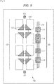
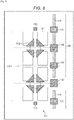
- Fig. 5 is a diagram illustrating an exemplary configuration of a solid-state imaging device to which the present technology is applied.
- the solid-state imaging device includes a backside illumination type CMOS sensor of 4-Tr. type, 8-pixel sharing (2 ⁇ 4 pixels) is illustrated.
- the 4-Tr. type has one area where three transistors including a reset Tr. (RST), an amplification Tr. (AMP), and a selection Tr. (SEL) described above are arranged besides a photodiode area where photodiodes are arranged. Further, it is assumed that the transfer Tr. is arranged in the photodiode area because the transfer Tr. is directly connected to the photodiode.
- RST reset Tr.
- AMP amplification Tr.
- SEL selection Tr.
- 2 ⁇ 4 pixels of photodiodes 111 which is a pixel sharing unit, and 2 ⁇ 4 pixels of transfer Trs. 112 are arranged as a PD group 121 in the photodiode area on the left side of the drawing.
- the 2 ⁇ 4 pixels of photodiodes 111 and the 2 ⁇ 4 pixels of transfer Trs. 112 of are arranged such that every 4 pixels are arrayed in two steps in a vertical direction of the drawing so as to form a vertically long rectangle.
- a selection Tr. 115, an amplification Tr. 116, a dummy Tr. 117, and a reset Tr. 118 which are directly connected to a source drain 114, are arranged as one Tr. group 122 in an area other than the photodiode on the right side of the drawing.
- the pixels Tr. including the selection Tr. 115, amplification Tr. 116, dummy Tr. 117, and reset Tr. 118 are arranged as one Tr. group 122 on a side of a long side of one PD group 121 including the 2 ⁇ 4 pixels of photodiodes 111.
- an L-length of the amplification Tr. 116 can be elongated (at least longer than other Trs.), thereby achieving improved RN (random noise) performance.
- the long side of the amplification Tr. is not necessarily equal to the L-length although the L-length direction is generally longer in the amplification Tr. in a viewpoint of RN and the L length is the long side in the present embodiment as well.
- the L-length represents a length of a direction linking the source-drain.
- the amplification Tr. 116 may have the L-length elongated.
- the selection Tr. 117 may have the L-length elongated. In the case of elongating the L-length of the selection Tr., a short channel effect may be reduced and a robust random noise margin may be obtained.
- the respective pixels Trs. of the Tr. group 122 are arranged so as to be positionally symmetric with respect to the respective photodiodes 111 of the PD group 121 (i.e., optically symmetric with respect to photodiodes).
- the amplification Tr. 116 is positioned beside the photodiode 111 at a lower right of upper-side 4 pixels, but there is no Tr. beside the photodiode 111 at the lower right of lower-side 4 pixels. Therefore, optical property may change due to difference of polysilicon density despite having a same color (e.g., green).
- the dummy Tr. 117 which is a dummy of the reset Tr. 118 is provided, and two reset Trs. are provided in the Tr. group 122. More specifically, the selection Tr. 115 and amplification Tr. 116 are provided near the transfer Tr. 112 on the upper-side 4 pixels, and the dummy Tr. 117 and reset Tr. 118 are provided near the transfer Tr. 112 on the lower-side 4 pixels.
- the dummy Tr. 117 is not necessarily driven as the Tr. In other words, the dummy Tr. 117 may be driven, or may just be provided without being driven.
- symmetry can be improved because layout substantially equivalent (sizes of gate, source, and drain) to the side of the selection Tr. 115 and amplification Tr. 116 can be obtained in the Tr. group 122 by the dummy Tr. 117 and reset Tr. 118 illustrated at the lower side of the drawing.
- PRNU photo response non uniformity: sensitivity ununiformity
- the dummy Tr. 117 is not limited to the dummy of the reset Tr. 118, and may be a dummy for other Trs.
- a well contact 113 is arranged between the PD group 121 and other PD groups 121 not illustrated but arranged on upper and lower sides of the drawing. With this arrangement, an area for the additional Tr. can be effectively secured. Note that an interval at which the PD groups 121 are arranged will be referred to as a pitch of the PD group 121 hereinafter.
- the well contact 113 influences various kinds of pixel characteristics (especially dark current)
- the difference between the pixels can be suppressed by arranging the well contact between the PD group 121 and other PD groups 121 arranged on the upper and lower sides of the drawing.
- the difference between the pixels can be small because the well contacts are positioned at equal intervals from all of the PDs by arranging the well contact 113 as described above.
- Fig. 6 is a diagram illustrating an exemplary arrangement of the photodiodes and Trs. in the solid-state imaging device to which the present technology is applied.
- the Tr. group 122 is arranged on the side of the long side of one PD group 121 including 2 ⁇ 4 pixels of photodiodes 111 in the same manner as the solid-state imaging device 101 in Fig. 5 . Therefore, as shown by the L-length of the amplification Tr. 116, the L-length of an existing Tr. can be elongated, thereby achieving improved RN (random noise) performance.
- the solid-state imaging device 151 in Fig. 6 differs from the solid-state imaging device 101 in Fig. 5 in that the dummy Tr. 117 is excluded from the Tr. group 122 and an arrangement position of the Tr. group 122 with respect to the PD group 121 is different.
- the amplification Tr. 116 is arranged beside the 4 pixels of transfer Trs. 112 on the upper side of the drawing, and the selection Tr. 115 and the reset Tr. 118 are arranged at corners of the 4 pixels of photodiodes 111 on a side where no transfer Tr. 112 is provided on the upper side of the drawing as indicated by arrows P1 and P2.
- the selection Tr. 115 of the Tr. group 122 corresponding to another PD group 121 arranged below the PD group 121 is also arranged at the corner of the 4 pixels of photo diodes 111 on the side where no transfer Tr. 112 is provided on the lower side of the drawing.
- Tr. group 122 is arranged entirely shifted to the upper side of the drawing with respect to the position of the PD group 121.
- the position of the PD group 121 and the position of the Tr. group 122 are aligned.
- Tr. group 122 is shifted upward by the length of the long side of one photodiode 111 with respect to a rectangular shaped sharing unit of the PD group 121. Note that a shifted amount is not limited to the length of the long side of the one photodiode 111. The same shall apply hereinafter.
- the well contact 113 is arranged beside the 4 pixels of transfer Trs. 112 on the lower side of the drawing in order to improve symmetry between the upper and lower 4 pixels of photodiodes 111 in the solid-state imaging device 151 of Fig. 6 .
- the amplification Tr. 116 and the well contact 113 are not necessarily positioned right beside the 4 pixels of transfer Trs. 112 respectively, and in the case of being positioned in the vicinity of right beside the transfer Tr. 112, an effect of symmetry improvement can be expected.
- PRNU can be improved without providing the dummy Tr. because symmetry with respect to the photodiodes 111 of the PD group 121 is achieved just by arranging one in each of the reset Tr., amplification Tr., and selection Tr. in the Tr. group 122.
- the well contact 113 may be arranged between the PD groups 121 in the same manner as the example in Fig. 5 .
- the positions of the respective Trs. of the Tr. group 122 may be arranged in accordance a layout whereby both PRNU and RN can be improved.
- a solid-state imaging device 201 in Fig. 7 differs from the solid-state imaging device 151 in Fig. 6 in that the amplification Tr. 116 is replaced by an amplification Tr. 211 having the L-length elongated at a maximum in the Tr. group 122.
- the L-length of the amplification Tr. 211 in the Tr. group 122 is larger than the L-length of the amplification Tr. 116 in Fig. 6 .
- the Tr. group 122 is arranged along the long side of the PD group 121 including the 2 ⁇ 8 pixels of photodiodes 111, in the same manner as the solid-state imaging device 101 in Fig. 5 . Therefore, RN (random noise) performed can be improved because the L-length of an existing Tr. can be elongated as shown by the L-length of the amplification Tr. 211.
- the amplification Tr. 211 is arranged beside the 4 pixels of transfer Trs. 112 on the upper side of the drawing, and further as indicated by arrows P11 and P12, the selection Tr. 115 and reset Tr. 118 are arranged at the corners of the 4 pixels of photodiodes 111 on the side where no transfer Tr. 112 is arranged on the upper side of the drawing. Additionally, as indicated by an arrow P13, the selection Tr. 115 of the Tr. group 122 corresponding to another PD group 121 (not shown) arranged below the illustrated PD group 121 is also arranged at the corner of the 4 pixels of the photodiodes 111 on the side where no transfer Tr. 112 is arranged on the lower side of the drawing.
- Tr. group 122 is arranged entirely shifted upward in the drawing with respect to the position of the PD group 121.
- the well contact 113 is arranged between the PD group 121 and another PD group 121 not illustrated but arranged on the lower side of the drawing in the same manner as the solid-state imaging device 101 in Fig. 5 .
- the difference between the pixels can be suppressed in the solid-state imaging device 201 of Fig. 7 , in a similar way as the solid-state imaging device 101 in Fig. 5 .
- the Tr. group 122 can be arranged in the same manner as the example in Fig. 6 .
- the polysilicon of the Trs. is arranged substantially uniformly with respect to the arrangement of the photodiodes 111 of the PD group 121 as illustrated in Fig. 8 , thereby achieving to improve PRNU.
- the selection Tr. 115 of the Tr. group 122 is arranged beside the well contact 113 arranged on the upper side of the PD group 121 in the drawing. Further, the amplification Tr. 116 is arranged beside the 4 pixels of transfer Trs. 112 in the PD group 121 on the upper side of the drawing, and the reset Tr. 118 is arranged between the 4 pixels of photodiodes 111 and the 4 pixels of photodiodes 111 in the PD group 121.
- the dummy Tr. 117 is arranged beside the 4 pixels of transfer Trs. 112 in the PD group 121 on the lower side of the drawing.
- the polysilicon of Trs. are arranged more uniformly with respect to the arrangement of the photodiodes of the PD group 121.
- the L-length of the amplification Tr. 116 cannot be elongated, compared to the solid-state imaging device 101 in Fig. 5 . Therefore, RN performance cannot be improved, but PRNU can be improved most.
- the well contact 113 is arranged between the PD group and PD group in the same manner as the solid-state imaging device 101 in Fig. 5 , the difference of the pixel characteristics between the pixels can be minimized. Note that the dummy Tr. 117 is not necessarily provided.
- the polysilicon beside the transfer Tr. 112 may not influence PRNU.
- the layout without having the dummy Tr. 117 may also be an option.
- Fig. 9 is a diagram illustrating another exemplary configuration of a solid-state imaging device to which the present technology is applied.
- the solid-state imaging device includes a backside illumination type CMOS sensor of 4-Tr. type, 2-pixel sharing (1 ⁇ 2 pixels).
- the example in Fig. 9 is a case in which the layout described in Fig. 5 is applied to the 2-pixel sharing.
- 1 ⁇ 2 pixels of photodiodes 111 adopting a pixel sharing structure and 1 ⁇ 2 pixels of transfer Trs. 112 corresponding thereto are arranged so as to form a vertically long rectangle as a PD group 121 in a photodiode area on a left side of the drawing.
- pixel Trs. including a selection Tr. 115, an amplification Tr. 116, a dummy Tr. 117, and a reset Tr. 118 are arranged as a Tr. group 122 on a side of a long side of the PD group 121.
- the respective pixel Trs. of the Tr. group 122 are arranged so as to be symmetric with respect to the respective photodiodes 111 of the PD group 121.
- the selection Tr. 115 is arranged in the vicinity of a center of the upper photodiode 111 of the PD group 121
- the reset Tr. 118 is arranged in the vicinity of a center of the lower photodiode 111 of the PD group 121 so as to be symmetric therewith.
- the amplification Tr. 116 is arranged in the vicinity of the upper transfer Tr. 112 of the PD group 121, and the dummy Tr. 117 is arranged in the vicinity of the lower transfer Tr. 112 of the PD group 121 so as to be symmetric therewith.
- RN random noise
- a well contact 113 is arranged between the Tr. group 122 and another Tr. group 122 positioned above, but may also be arranged between the PD and the PD as in an example shown in Fig. 8 .
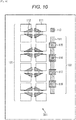
- Fig. 10 is a diagram illustrating another exemplary configuration of a solid-state imaging device to which the present technology is applied.
- the solid-state imaging device includes a backside illumination type CMOS sensor of 4-Tr. type, 16-pixel sharing (2 ⁇ 8 pixels).
- CMOS sensor of 4-Tr. type
- 16-pixel sharing (2 ⁇ 8 pixels).
- the example in Fig. 10 is the case in which the layout described in Fig. 5 is applied to the 16-pixel sharing.
- 2 ⁇ 8 pixels of photodiodes 111 adopting a pixel sharing structure and 2 ⁇ 8 pixels of transfer Trs. 112 corresponding thereto are arranged as one PD group 121 in the photodiode area on a left side of the drawing.
- the 2 ⁇ 8 pixels of photodiodes 111 and the 2 ⁇ 8 pixels of transfer Trs. 112 are arranged so as to form a vertically long rectangle, and every 4 pixels are arrayed in four steps in a vertical direction of the drawing.
- pixel Trs. including a selection Tr. 115, an amplification Tr. 116, a dummy Tr. 117, and a reset Tr. 118 are arranged as one Tr. group 122 on a side of a long side of the PD group 121 (right side in the drawing).
- a well contact 113 is arranged on an upper side of the Tr. group 122 in the drawing. The well contact 113 and the respective pixel Trs. of the Tr. group 122 are arranged so as to be symmetric with respect to the respective photodiodes 111 of the PD group 121.
- the well contact 113 is arranged in the vicinity of right beside the 4 pixels of transfer Trs. 112 in a first step from the top of the drawing.
- the selection Tr. 115 is arranged in the vicinity of a position opposite to the transfer Trs. 112 of the 4 pixels of photodiodes 111 in a second step from the top of the drawing in the PD group 121.
- the amplification Tr. 116 is arranged in the vicinity of positions of the transfer Trs. 112 of the 4 pixels of photodiodes 111 in the second step from the top of the drawing in the PD group 121.
- the dummy Tr. 117 is arranged in the vicinity of the positions of the transfer Trs. 112 of the 4 pixels of photodiodes 111 in a third step from the top of the drawing in the PD group 121.
- the reset Tr. 118 is arranged in the vicinity of a position opposite to the transfer Trs. 112 of the photodiodes 111 in a fourth step from the top of the drawing in the PD group 121.
- an L-length of an existing Tr. can be elongated as shown by the L-length of an amplification Tr. 116 because the Tr. group 122 is arranged on a side of a long side of one PD group 121 including 2 ⁇ 8 pixels of the photodiodes 111 in the same manner as the solid-state imaging device 101 in Fig. 5 .
- RN performance can be improved.
- PRNU can be improved.
- the well contact 113 is arranged between the Tr. group 122 and another Tr. group 122 positioned above, and the well contact 113 is not provided between the PD groups 121. Therefore, influence caused by a difference between the pixels may remain.
- the well contact 113 can be arranged between the PD and the PD as in an example shown in Fig. 5 . In the case of arranging the well contact 113 between the 4 pixels of the respective steps, the difference of the characteristic between the pixels may be reduced.
- the present technology is applicable in the case where the sharing unit is shaped in a rectangle such as 2-pixel sharing, 8-pixel sharing, and 16-pixel sharing of 4-Tr. type.
- the number of pixels to be shared is not limited, and arrangement of the solid-state imaging device is not limited to the above-described arrangement examples as long as arrangement of the photodiodes in the one sharing unit is shaped in a rectangle.
- Trs. varied arrangement of 4-Tr. type, 8-pixel sharing (2 ⁇ 4 pixels) described above in a first embodiment can be applied to 2-pixel sharing and 16-pixel sharing.
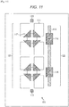
- Fig. 11 is a diagram illustrating an exemplary configuration of a solid-state imaging device to which the present technology is applied.
- the solid-state imaging device includes a backside illumination type CMOS sensor of 3-Tr. type, 8-pixel sharing (2 ⁇ 4 pixels).
- a solid-state imaging device 401 in Fig. 11 differs from a solid-state imaging device 101 in Fig. 5 in that a selection Tr. 115 and a dummy Tr. 117 are excluded from one Tr. group 122.
- the solid-state imaging device 401 of Fig. 11 is in common with the solid-state imaging device 101 in Fig. 5 in a point of being arranged within a rectangular shaped sharing unit (a PD group is arranged right beside a Tr. group).
- an amplification Tr. 116 is arranged beside 4 pixels of transfer Trs. 112 on an upper side of the drawing, and a reset Tr. 118 is arranged beside 4 pixels of transfer Trs. 112 of on a lower side of the drawing.
- the amplification Tr. 116 and the reset Tr. 118 are formed in a substantially same size.
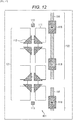
- an arrangement position of the Tr. group 122 in Fig. 11 is shifted upward by about a length of a long side of one photodiode 111 in the drawing. More specifically, in the Tr. group 122, the amplification Tr. 116 is arranged beside the 4 pixels of photodiodes 111 but not on a side of the transfer Trs. 112 on the upper side of the drawing, and the reset Tr. 118 is arranged beside the 4 pixels of photodiodes 111 but not on the side of the transfer Trs. 112 on the lower side of the drawing. In the example of Fig. 12 also, the amplification Tr. 116 and the reset Tr. 118 are formed in a substantially same size.
- an L-length of an existing Tr. can be elongated as shown by the L-length of the amplification Tr. 116 because the Tr. group 122 is arranged along a long side of the PD group 121.
- RN performance can be improved.
- PRNU can be improved because polysilicon of the Trs. is symmetric with respect to the photodiodes.
- the present technology is applicable to all of the cases in which the sharing unit is in the shape of a rectangle.
- the number of pixels to be shared is not limited, and arrangement of the solid-state imaging device is not limited to the above-described arrangement examples as long as the arrangement of the photodiodes in the one sharing unit is shaped in a rectangle.
- RN random noise margin or performance can be improved because the L-length of the Tr. (particularly, amplification Tr.) can be elongated.
- the required number of source drains is three in the group 1 and three in the group 2, i.e., six in total.
- there is a limit in elongating the L-length of the Tr. because of limitation in a lithography line width, limitation in processing the polysilicon and a contact hole, securing isolation breakdown voltage, and so on.
- the influence from such a state is quite serious, and RN margin may be deteriorated due to the short L-length of the AMP.
- RN performance can be improved because the L-length of the amplification Tr. can be elongated.
- the L-length of the amplification Tr. is 0.6 to 1.4 times of a pitch of the PD group in the above-described example.
- the L-length of the selection Tr. can be elongated. Therefore, in the case of elongating an L-length of the selection Tr., a short channel effect may be avoided and a robust random noise margin property may be obtained.
- PRNU can be improved because arrangement is made so as to have symmetry of the polysilicon of the Trs.
- the present technology may be applied to the solid-state imaging device such as a CCD (charge coupled device) solid-state imaging device.
- CCD charge coupled device
- the solid-state imaging device may be either a backside illumination type or a front side illumination type.
- the solid-state imaging device may be either a global shutter type or not.
- the solid-state imaging device is not limited to the global shutter type.
- the imaging device means a camera system such as a digital still camera and a digital video camera, and an electronic apparatus provided with an imaging function, such as a cell phone.
- the image device may have a module type configuration, namely, a camera module, mounted on the electronic apparatus.
- An electronic apparatus 500 illustrated in Fig. 13 includes a solid-state imaging device (device chip) 501, an optical lens 502, a shutter device 503, a drive circuit 504, and a signal processing circuit 505.
- a solid-state imaging device device chip
- an optical lens 502 an optical lens
- a shutter device 503 a drive circuit 504
- the solid-state imaging device 501 a solid-state imaging device according to above-described first to fourth embodiments of the present technology is provided. Therefore, the electronic apparatus 500 having high performance and provided with improved RN performance and PRNU can be provided.
- the optical lens 502 forms, on an imaging surface of the solid-state imaging device 501, an image light (incident light) from an object. By this, signal charge is accumulated inside the solid-state imaging device 501 for a predetermined period.
- the shutter device 503 controls an irradiation time and a shielding time for the solid-state imaging device 501.
- the drive circuit 504 supplies a drive signal that controls signal transfer operation of the solid-state imaging device 501 and shutter operation of the shutter device 503.
- the solid-state imaging device 501 transfers a signal in accordance with the drive signal (timing signal) supplied from the drive circuit 504.
- the signal processing circuit 505 executes various kinds of signal processing for the signal output from the solid-state imaging device 501.
- a video signal applied with the signal processing is stored in a storage medium such as a memory, or output to a monitor.
- steps to describe a series of the above-described processing may obviously include the processing executed in time series in accordance with the described order, but also may include processing executed in parallel or individually although not constantly executed in time series.
- one step includes a plurality of processing
- the plurality of processing included in the one step may be executed by one device and also by a plurality of devices in a sharing manner.
- the configuration described above as one device (or processing section) may be divided, and may be configured as a plurality of devices (or processing sections).
- the configuration described above as the plurality of devices (or processing sections) may be integrally configured as one device (or processing section).
- the respective devices (or respective processing section) may be added with a configuration other than the above-described configuration.
- a part of a configuration of a device (or processing section) may be included in other devices (or other processing sections).
- the present technology is not limited to the above-described embodiments, and various kinds of changes may be made in the scope without departing from the gist of the present technology.
Landscapes
- Engineering & Computer Science (AREA)
- Physics & Mathematics (AREA)
- Power Engineering (AREA)
- Electromagnetism (AREA)
- Condensed Matter Physics & Semiconductors (AREA)
- General Physics & Mathematics (AREA)
- Computer Hardware Design (AREA)
- Microelectronics & Electronic Packaging (AREA)
- Multimedia (AREA)
- Signal Processing (AREA)
- Solid State Image Pick-Up Elements (AREA)
- Transforming Light Signals Into Electric Signals (AREA)
Applications Claiming Priority (3)
| Application Number | Priority Date | Filing Date | Title |
|---|---|---|---|
| JP2014038584A JP6334203B2 (ja) | 2014-02-28 | 2014-02-28 | 固体撮像装置、および電子機器 |
| EP15711310.1A EP3111631B1 (en) | 2014-02-28 | 2015-02-20 | Imaging device and electronic apparatus |
| PCT/JP2015/000821 WO2015129226A1 (en) | 2014-02-28 | 2015-02-20 | Imaging device and electronic apparatus |
Related Parent Applications (2)
| Application Number | Title | Priority Date | Filing Date |
|---|---|---|---|
| EP15711310.1A Division EP3111631B1 (en) | 2014-02-28 | 2015-02-20 | Imaging device and electronic apparatus |
| EP15711310.1A Division-Into EP3111631B1 (en) | 2014-02-28 | 2015-02-20 | Imaging device and electronic apparatus |
Publications (2)
| Publication Number | Publication Date |
|---|---|
| EP3518518A1 EP3518518A1 (en) | 2019-07-31 |
| EP3518518B1 true EP3518518B1 (en) | 2020-08-12 |
Family
ID=52697493
Family Applications (2)
| Application Number | Title | Priority Date | Filing Date |
|---|---|---|---|
| EP19154945.0A Active EP3518518B1 (en) | 2014-02-28 | 2015-02-20 | Imaging device and electronic apparatus |
| EP15711310.1A Active EP3111631B1 (en) | 2014-02-28 | 2015-02-20 | Imaging device and electronic apparatus |
Family Applications After (1)
| Application Number | Title | Priority Date | Filing Date |
|---|---|---|---|
| EP15711310.1A Active EP3111631B1 (en) | 2014-02-28 | 2015-02-20 | Imaging device and electronic apparatus |
Country Status (7)
| Country | Link |
|---|---|
| US (4) | US10075659B2 (ja) |
| EP (2) | EP3518518B1 (ja) |
| JP (1) | JP6334203B2 (ja) |
| KR (3) | KR20230019213A (ja) |
| CN (2) | CN111312736B (ja) |
| TW (1) | TWI653891B (ja) |
| WO (1) | WO2015129226A1 (ja) |
Families Citing this family (15)
| Publication number | Priority date | Publication date | Assignee | Title |
|---|---|---|---|---|
| JP6334203B2 (ja) * | 2014-02-28 | 2018-05-30 | ソニー株式会社 | 固体撮像装置、および電子機器 |
| TWI696278B (zh) | 2015-03-31 | 2020-06-11 | 日商新力股份有限公司 | 影像感測器、攝像裝置及電子機器 |
| JP6491519B2 (ja) * | 2015-04-02 | 2019-03-27 | キヤノン株式会社 | 撮像素子及び撮像装置 |
| KR102541701B1 (ko) | 2016-01-15 | 2023-06-13 | 삼성전자주식회사 | 씨모스 이미지 센서 |
| WO2018068322A1 (en) * | 2016-10-14 | 2018-04-19 | Huawei Technologies Co., Ltd. | Cmos image sensor |
| KR20180076054A (ko) | 2016-12-27 | 2018-07-05 | 삼성전자주식회사 | 공유 픽셀을 구비한 이미지 센서 및 그 이미지 센서를 구비한 전자 장치 |
| KR20180076845A (ko) | 2016-12-28 | 2018-07-06 | 삼성전자주식회사 | 이미지 센서 |
| KR102333610B1 (ko) * | 2017-03-06 | 2021-12-03 | 에스케이하이닉스 주식회사 | 이미지 센서 |
| KR102380819B1 (ko) * | 2017-04-12 | 2022-03-31 | 삼성전자주식회사 | 이미지 센서 |
| JP2018207291A (ja) * | 2017-06-05 | 2018-12-27 | ソニーセミコンダクタソリューションズ株式会社 | 固体撮像素子および撮像装置 |
| KR102356913B1 (ko) * | 2017-07-03 | 2022-02-03 | 에스케이하이닉스 주식회사 | 이미지 센서 |
| KR102551862B1 (ko) * | 2018-01-29 | 2023-07-06 | 에스케이하이닉스 주식회사 | 이미지 센서 |
| KR102568744B1 (ko) * | 2018-01-29 | 2023-08-22 | 에스케이하이닉스 주식회사 | 이미지 센서 |
| JP7086783B2 (ja) | 2018-08-13 | 2022-06-20 | 株式会社東芝 | 固体撮像装置 |
| KR102358599B1 (ko) * | 2019-09-30 | 2022-02-08 | 선전 구딕스 테크놀로지 컴퍼니, 리미티드 | 이미지 센서의 반도체 구조, 칩 및 전자 장치 |
Family Cites Families (31)
| Publication number | Priority date | Publication date | Assignee | Title |
|---|---|---|---|---|
| US6657665B1 (en) * | 1998-12-31 | 2003-12-02 | Eastman Kodak Company | Active Pixel Sensor with wired floating diffusions and shared amplifier |
| US20050128327A1 (en) * | 2003-12-10 | 2005-06-16 | Bencuya Selim S. | Device and method for image sensing |
| US7635880B2 (en) * | 2004-12-30 | 2009-12-22 | Ess Technology, Inc. | Method and apparatus for proximate CMOS pixels |
| JP2007095917A (ja) * | 2005-09-28 | 2007-04-12 | Matsushita Electric Ind Co Ltd | 固体撮像装置 |
| JP4752447B2 (ja) | 2005-10-21 | 2011-08-17 | ソニー株式会社 | 固体撮像装置およびカメラ |
| US20070131992A1 (en) * | 2005-12-13 | 2007-06-14 | Dialog Semiconductor Gmbh | Multiple photosensor pixel image sensor |
| JP4350768B2 (ja) * | 2007-04-16 | 2009-10-21 | キヤノン株式会社 | 光電変換装置及び撮像装置 |
| US7964929B2 (en) | 2007-08-23 | 2011-06-21 | Aptina Imaging Corporation | Method and apparatus providing imager pixels with shared pixel components |
| US7989749B2 (en) * | 2007-10-05 | 2011-08-02 | Aptina Imaging Corporation | Method and apparatus providing shared pixel architecture |
| JP5292787B2 (ja) * | 2007-11-30 | 2013-09-18 | ソニー株式会社 | 固体撮像装置及びカメラ |
| JP4630907B2 (ja) * | 2008-03-03 | 2011-02-09 | シャープ株式会社 | 固体撮像装置および電子情報機器 |
| JP5178266B2 (ja) * | 2008-03-19 | 2013-04-10 | キヤノン株式会社 | 固体撮像装置 |
| JP5188275B2 (ja) * | 2008-06-06 | 2013-04-24 | キヤノン株式会社 | 固体撮像装置、その駆動方法及び撮像システム |
| JP2009302483A (ja) * | 2008-06-17 | 2009-12-24 | Panasonic Corp | 固体撮像装置及びその製造方法 |
| US20100230583A1 (en) * | 2008-11-06 | 2010-09-16 | Sony Corporation | Solid state image pickup device, method of manufacturing the same, image pickup device, and electronic device |
| JP5029624B2 (ja) * | 2009-01-15 | 2012-09-19 | ソニー株式会社 | 固体撮像装置及び電子機器 |
| TWI425629B (zh) * | 2009-03-30 | 2014-02-01 | Sony Corp | 固態影像拾取裝置及其製造方法,影像拾取裝置及電子裝置 |
| TWI411102B (zh) * | 2009-03-31 | 2013-10-01 | Sony Corp | 固態成像元件及成像裝置 |
| JP5564874B2 (ja) * | 2009-09-25 | 2014-08-06 | ソニー株式会社 | 固体撮像装置、及び電子機器 |
| JP5564909B2 (ja) | 2009-11-30 | 2014-08-06 | ソニー株式会社 | 固体撮像装置とその製造方法、及び電子機器 |
| JP2011114324A (ja) * | 2009-11-30 | 2011-06-09 | Sony Corp | 固体撮像装置及び電子機器 |
| JP5537172B2 (ja) | 2010-01-28 | 2014-07-02 | ソニー株式会社 | 固体撮像装置及び電子機器 |
| JP6003291B2 (ja) | 2011-08-22 | 2016-10-05 | ソニー株式会社 | 固体撮像装置及び電子機器 |
| JP6026102B2 (ja) * | 2011-12-07 | 2016-11-16 | ソニーセミコンダクタソリューションズ株式会社 | 固体撮像素子および電子機器 |
| WO2013157407A1 (ja) * | 2012-04-19 | 2013-10-24 | 国立大学法人東北大学 | 固体撮像装置 |
| US9305949B2 (en) * | 2013-11-01 | 2016-04-05 | Omnivision Technologies, Inc. | Big-small pixel scheme for image sensors |
| JP6334203B2 (ja) * | 2014-02-28 | 2018-05-30 | ソニー株式会社 | 固体撮像装置、および電子機器 |
| TWI696278B (zh) * | 2015-03-31 | 2020-06-11 | 日商新力股份有限公司 | 影像感測器、攝像裝置及電子機器 |
| KR20180077969A (ko) * | 2016-12-29 | 2018-07-09 | 삼성전자주식회사 | 이미지 센서 및 그 이미지 센서를 구비한 전자 장치 |
| KR102638779B1 (ko) * | 2017-01-03 | 2024-02-22 | 삼성전자주식회사 | 이미지 센서 |
| JP6964479B2 (ja) | 2017-10-03 | 2021-11-10 | エヌ・イーケムキャット株式会社 | 希土類元素骨格置換ゼオライト及びその製造方法、並びにこれらを用いたNOx吸着材、選択的還元触媒及び自動車排ガス触媒 |
-
2014
- 2014-02-28 JP JP2014038584A patent/JP6334203B2/ja active Active
-
2015
- 2015-02-04 TW TW104103789A patent/TWI653891B/zh active
- 2015-02-20 CN CN202010118252.XA patent/CN111312736B/zh active Active
- 2015-02-20 EP EP19154945.0A patent/EP3518518B1/en active Active
- 2015-02-20 KR KR1020237002324A patent/KR20230019213A/ko active IP Right Grant
- 2015-02-20 KR KR1020167022090A patent/KR102386941B1/ko active IP Right Grant
- 2015-02-20 CN CN201580009596.4A patent/CN106030804B/zh active Active
- 2015-02-20 WO PCT/JP2015/000821 patent/WO2015129226A1/en active Application Filing
- 2015-02-20 KR KR1020227007266A patent/KR102492853B1/ko active IP Right Grant
- 2015-02-20 US US15/119,499 patent/US10075659B2/en active Active
- 2015-02-20 EP EP15711310.1A patent/EP3111631B1/en active Active
-
2018
- 2018-09-05 US US16/122,753 patent/US11044428B2/en active Active
-
2020
- 2020-07-20 US US16/933,379 patent/US11683601B2/en active Active
-
2023
- 2023-04-13 US US18/300,062 patent/US20230247317A1/en active Pending
Non-Patent Citations (1)
| Title |
|---|
| None * |
Also Published As
| Publication number | Publication date |
|---|---|
| US20170013211A1 (en) | 2017-01-12 |
| TW201534121A (zh) | 2015-09-01 |
| US10075659B2 (en) | 2018-09-11 |
| JP2015162646A (ja) | 2015-09-07 |
| US20190007631A1 (en) | 2019-01-03 |
| KR102386941B1 (ko) | 2022-04-15 |
| US20200366856A1 (en) | 2020-11-19 |
| KR20220034926A (ko) | 2022-03-18 |
| KR20230019213A (ko) | 2023-02-07 |
| US11044428B2 (en) | 2021-06-22 |
| EP3111631B1 (en) | 2019-04-03 |
| TWI653891B (zh) | 2019-03-11 |
| CN111312736A (zh) | 2020-06-19 |
| EP3518518A1 (en) | 2019-07-31 |
| CN111312736B (zh) | 2023-10-24 |
| KR20160127730A (ko) | 2016-11-04 |
| CN106030804B (zh) | 2020-03-20 |
| WO2015129226A1 (en) | 2015-09-03 |
| US11683601B2 (en) | 2023-06-20 |
| EP3111631A1 (en) | 2017-01-04 |
| CN106030804A (zh) | 2016-10-12 |
| JP6334203B2 (ja) | 2018-05-30 |
| US20230247317A1 (en) | 2023-08-03 |
| KR102492853B1 (ko) | 2023-01-31 |
Similar Documents
| Publication | Publication Date | Title |
|---|---|---|
| US11683601B2 (en) | Imaging device and electronic apparatus | |
| US10057519B2 (en) | Solid-state imaging device and imaging system | |
| US9992417B2 (en) | Solid-state imaging device, method for driving solid-state imaging device, and electronic apparatus | |
| US8179461B2 (en) | Solid-state image pickup device, method for driving solid-state image pickup device, and image pickup apparatus | |
| US8134625B2 (en) | Solid-state imaging device, camera, and electronic device | |
| JP5987326B2 (ja) | 固体撮像素子および信号処理方法、並びに電子機器 | |
| KR20160001918U (ko) | 향상된 셔터 효율을 가지는 글로벌 셔터 이미지 센서 픽셀들 | |
| US20150028189A1 (en) | Solid-state imaging device, driving method thereof and electronic apparatus | |
| JP2016005068A (ja) | 固体撮像装置および電子機器 | |
| JP2018098772A (ja) | 撮像素子および電子機器 | |
| US9190449B2 (en) | Image pickup apparatus including signal holding units | |
| US8957360B2 (en) | Method for driving photoelectric conversion apparatus | |
| JP2017139498A (ja) | 固体撮像装置、および電子機器 | |
| US20230412944A1 (en) | Solid-state imaging element, electronic device, and control method of solid-state imaging element |
Legal Events
| Date | Code | Title | Description |
|---|---|---|---|
| PUAI | Public reference made under article 153(3) epc to a published international application that has entered the european phase |
Free format text: ORIGINAL CODE: 0009012 |
|
| STAA | Information on the status of an ep patent application or granted ep patent |
Free format text: STATUS: REQUEST FOR EXAMINATION WAS MADE |
|
| 17P | Request for examination filed |
Effective date: 20190131 |
|
| AC | Divisional application: reference to earlier application |
Ref document number: 3111631 Country of ref document: EP Kind code of ref document: P |
|
| AK | Designated contracting states |
Kind code of ref document: A1 Designated state(s): AL AT BE BG CH CY CZ DE DK EE ES FI FR GB GR HR HU IE IS IT LI LT LU LV MC MK MT NL NO PL PT RO RS SE SI SK SM TR |
|
| GRAP | Despatch of communication of intention to grant a patent |
Free format text: ORIGINAL CODE: EPIDOSNIGR1 |
|
| STAA | Information on the status of an ep patent application or granted ep patent |
Free format text: STATUS: GRANT OF PATENT IS INTENDED |
|
| RIC1 | Information provided on ipc code assigned before grant |
Ipc: H04N 5/3745 20110101ALI20200205BHEP Ipc: H01L 27/146 20060101ALI20200205BHEP Ipc: H04N 5/378 20110101ALI20200205BHEP Ipc: H04N 5/357 20110101ALI20200205BHEP Ipc: H04N 5/217 20110101AFI20200205BHEP |
|
| INTG | Intention to grant announced |
Effective date: 20200303 |
|
| GRAS | Grant fee paid |
Free format text: ORIGINAL CODE: EPIDOSNIGR3 |
|
| GRAA | (expected) grant |
Free format text: ORIGINAL CODE: 0009210 |
|
| STAA | Information on the status of an ep patent application or granted ep patent |
Free format text: STATUS: THE PATENT HAS BEEN GRANTED |
|
| AC | Divisional application: reference to earlier application |
Ref document number: 3111631 Country of ref document: EP Kind code of ref document: P |
|
| AK | Designated contracting states |
Kind code of ref document: B1 Designated state(s): AL AT BE BG CH CY CZ DE DK EE ES FI FR GB GR HR HU IE IS IT LI LT LU LV MC MK MT NL NO PL PT RO RS SE SI SK SM TR |
|
| REG | Reference to a national code |
Ref country code: CH Ref legal event code: EP |
|
| REG | Reference to a national code |
Ref country code: IE Ref legal event code: FG4D |
|
| REG | Reference to a national code |
Ref country code: DE Ref legal event code: R096 Ref document number: 602015057576 Country of ref document: DE |
|
| REG | Reference to a national code |
Ref country code: AT Ref legal event code: REF Ref document number: 1302713 Country of ref document: AT Kind code of ref document: T Effective date: 20200915 |
|
| REG | Reference to a national code |
Ref country code: NL Ref legal event code: FP |
|
| REG | Reference to a national code |
Ref country code: LT Ref legal event code: MG4D |
|
| PG25 | Lapsed in a contracting state [announced via postgrant information from national office to epo] |
Ref country code: HR Free format text: LAPSE BECAUSE OF FAILURE TO SUBMIT A TRANSLATION OF THE DESCRIPTION OR TO PAY THE FEE WITHIN THE PRESCRIBED TIME-LIMIT Effective date: 20200812 Ref country code: FI Free format text: LAPSE BECAUSE OF FAILURE TO SUBMIT A TRANSLATION OF THE DESCRIPTION OR TO PAY THE FEE WITHIN THE PRESCRIBED TIME-LIMIT Effective date: 20200812 Ref country code: GR Free format text: LAPSE BECAUSE OF FAILURE TO SUBMIT A TRANSLATION OF THE DESCRIPTION OR TO PAY THE FEE WITHIN THE PRESCRIBED TIME-LIMIT Effective date: 20201113 Ref country code: NO Free format text: LAPSE BECAUSE OF FAILURE TO SUBMIT A TRANSLATION OF THE DESCRIPTION OR TO PAY THE FEE WITHIN THE PRESCRIBED TIME-LIMIT Effective date: 20201112 Ref country code: LT Free format text: LAPSE BECAUSE OF FAILURE TO SUBMIT A TRANSLATION OF THE DESCRIPTION OR TO PAY THE FEE WITHIN THE PRESCRIBED TIME-LIMIT Effective date: 20200812 Ref country code: BG Free format text: LAPSE BECAUSE OF FAILURE TO SUBMIT A TRANSLATION OF THE DESCRIPTION OR TO PAY THE FEE WITHIN THE PRESCRIBED TIME-LIMIT Effective date: 20201112 Ref country code: SE Free format text: LAPSE BECAUSE OF FAILURE TO SUBMIT A TRANSLATION OF THE DESCRIPTION OR TO PAY THE FEE WITHIN THE PRESCRIBED TIME-LIMIT Effective date: 20200812 |
|
| REG | Reference to a national code |
Ref country code: AT Ref legal event code: MK05 Ref document number: 1302713 Country of ref document: AT Kind code of ref document: T Effective date: 20200812 |
|
| PG25 | Lapsed in a contracting state [announced via postgrant information from national office to epo] |
Ref country code: IS Free format text: LAPSE BECAUSE OF FAILURE TO SUBMIT A TRANSLATION OF THE DESCRIPTION OR TO PAY THE FEE WITHIN THE PRESCRIBED TIME-LIMIT Effective date: 20201212 Ref country code: RS Free format text: LAPSE BECAUSE OF FAILURE TO SUBMIT A TRANSLATION OF THE DESCRIPTION OR TO PAY THE FEE WITHIN THE PRESCRIBED TIME-LIMIT Effective date: 20200812 Ref country code: PL Free format text: LAPSE BECAUSE OF FAILURE TO SUBMIT A TRANSLATION OF THE DESCRIPTION OR TO PAY THE FEE WITHIN THE PRESCRIBED TIME-LIMIT Effective date: 20200812 Ref country code: LV Free format text: LAPSE BECAUSE OF FAILURE TO SUBMIT A TRANSLATION OF THE DESCRIPTION OR TO PAY THE FEE WITHIN THE PRESCRIBED TIME-LIMIT Effective date: 20200812 |
|
| PG25 | Lapsed in a contracting state [announced via postgrant information from national office to epo] |
Ref country code: CZ Free format text: LAPSE BECAUSE OF FAILURE TO SUBMIT A TRANSLATION OF THE DESCRIPTION OR TO PAY THE FEE WITHIN THE PRESCRIBED TIME-LIMIT Effective date: 20200812 Ref country code: DK Free format text: LAPSE BECAUSE OF FAILURE TO SUBMIT A TRANSLATION OF THE DESCRIPTION OR TO PAY THE FEE WITHIN THE PRESCRIBED TIME-LIMIT Effective date: 20200812 Ref country code: RO Free format text: LAPSE BECAUSE OF FAILURE TO SUBMIT A TRANSLATION OF THE DESCRIPTION OR TO PAY THE FEE WITHIN THE PRESCRIBED TIME-LIMIT Effective date: 20200812 Ref country code: EE Free format text: LAPSE BECAUSE OF FAILURE TO SUBMIT A TRANSLATION OF THE DESCRIPTION OR TO PAY THE FEE WITHIN THE PRESCRIBED TIME-LIMIT Effective date: 20200812 Ref country code: SM Free format text: LAPSE BECAUSE OF FAILURE TO SUBMIT A TRANSLATION OF THE DESCRIPTION OR TO PAY THE FEE WITHIN THE PRESCRIBED TIME-LIMIT Effective date: 20200812 |
|
| REG | Reference to a national code |
Ref country code: DE Ref legal event code: R097 Ref document number: 602015057576 Country of ref document: DE |
|
| PG25 | Lapsed in a contracting state [announced via postgrant information from national office to epo] |
Ref country code: ES Free format text: LAPSE BECAUSE OF FAILURE TO SUBMIT A TRANSLATION OF THE DESCRIPTION OR TO PAY THE FEE WITHIN THE PRESCRIBED TIME-LIMIT Effective date: 20200812 Ref country code: AT Free format text: LAPSE BECAUSE OF FAILURE TO SUBMIT A TRANSLATION OF THE DESCRIPTION OR TO PAY THE FEE WITHIN THE PRESCRIBED TIME-LIMIT Effective date: 20200812 Ref country code: AL Free format text: LAPSE BECAUSE OF FAILURE TO SUBMIT A TRANSLATION OF THE DESCRIPTION OR TO PAY THE FEE WITHIN THE PRESCRIBED TIME-LIMIT Effective date: 20200812 |
|
| PLBE | No opposition filed within time limit |
Free format text: ORIGINAL CODE: 0009261 |
|
| STAA | Information on the status of an ep patent application or granted ep patent |
Free format text: STATUS: NO OPPOSITION FILED WITHIN TIME LIMIT |
|
| PG25 | Lapsed in a contracting state [announced via postgrant information from national office to epo] |
Ref country code: SK Free format text: LAPSE BECAUSE OF FAILURE TO SUBMIT A TRANSLATION OF THE DESCRIPTION OR TO PAY THE FEE WITHIN THE PRESCRIBED TIME-LIMIT Effective date: 20200812 |
|
| 26N | No opposition filed |
Effective date: 20210514 |
|
| PG25 | Lapsed in a contracting state [announced via postgrant information from national office to epo] |
Ref country code: IT Free format text: LAPSE BECAUSE OF FAILURE TO SUBMIT A TRANSLATION OF THE DESCRIPTION OR TO PAY THE FEE WITHIN THE PRESCRIBED TIME-LIMIT Effective date: 20200812 |
|
| PG25 | Lapsed in a contracting state [announced via postgrant information from national office to epo] |
Ref country code: SI Free format text: LAPSE BECAUSE OF FAILURE TO SUBMIT A TRANSLATION OF THE DESCRIPTION OR TO PAY THE FEE WITHIN THE PRESCRIBED TIME-LIMIT Effective date: 20200812 |
|
| PG25 | Lapsed in a contracting state [announced via postgrant information from national office to epo] |
Ref country code: MC Free format text: LAPSE BECAUSE OF FAILURE TO SUBMIT A TRANSLATION OF THE DESCRIPTION OR TO PAY THE FEE WITHIN THE PRESCRIBED TIME-LIMIT Effective date: 20200812 |
|
| GBPC | Gb: european patent ceased through non-payment of renewal fee |
Effective date: 20210220 |
|
| REG | Reference to a national code |
Ref country code: BE Ref legal event code: MM Effective date: 20210228 |
|
| PG25 | Lapsed in a contracting state [announced via postgrant information from national office to epo] |
Ref country code: CH Free format text: LAPSE BECAUSE OF NON-PAYMENT OF DUE FEES Effective date: 20210228 Ref country code: LU Free format text: LAPSE BECAUSE OF NON-PAYMENT OF DUE FEES Effective date: 20210220 Ref country code: LI Free format text: LAPSE BECAUSE OF NON-PAYMENT OF DUE FEES Effective date: 20210228 |
|
| PG25 | Lapsed in a contracting state [announced via postgrant information from national office to epo] |
Ref country code: FR Free format text: LAPSE BECAUSE OF NON-PAYMENT OF DUE FEES Effective date: 20210228 Ref country code: GB Free format text: LAPSE BECAUSE OF NON-PAYMENT OF DUE FEES Effective date: 20210220 Ref country code: IE Free format text: LAPSE BECAUSE OF NON-PAYMENT OF DUE FEES Effective date: 20210220 |
|
| PG25 | Lapsed in a contracting state [announced via postgrant information from national office to epo] |
Ref country code: BE Free format text: LAPSE BECAUSE OF NON-PAYMENT OF DUE FEES Effective date: 20210228 |
|
| REG | Reference to a national code |
Ref country code: DE Ref legal event code: R079 Ref document number: 602015057576 Country of ref document: DE Free format text: PREVIOUS MAIN CLASS: H04N0005217000 Ipc: H04N0023800000 |
|
| PG25 | Lapsed in a contracting state [announced via postgrant information from national office to epo] |
Ref country code: PT Free format text: LAPSE BECAUSE OF FAILURE TO SUBMIT A TRANSLATION OF THE DESCRIPTION OR TO PAY THE FEE WITHIN THE PRESCRIBED TIME-LIMIT Effective date: 20201214 |
|
| PG25 | Lapsed in a contracting state [announced via postgrant information from national office to epo] |
Ref country code: CY Free format text: LAPSE BECAUSE OF FAILURE TO SUBMIT A TRANSLATION OF THE DESCRIPTION OR TO PAY THE FEE WITHIN THE PRESCRIBED TIME-LIMIT Effective date: 20200812 |
|
| P01 | Opt-out of the competence of the unified patent court (upc) registered |
Effective date: 20230528 |
|
| PG25 | Lapsed in a contracting state [announced via postgrant information from national office to epo] |
Ref country code: HU Free format text: LAPSE BECAUSE OF FAILURE TO SUBMIT A TRANSLATION OF THE DESCRIPTION OR TO PAY THE FEE WITHIN THE PRESCRIBED TIME-LIMIT; INVALID AB INITIO Effective date: 20150220 |
|
| PGFP | Annual fee paid to national office [announced via postgrant information from national office to epo] |
Ref country code: NL Payment date: 20240123 Year of fee payment: 10 |
|
| PG25 | Lapsed in a contracting state [announced via postgrant information from national office to epo] |
Ref country code: MK Free format text: LAPSE BECAUSE OF FAILURE TO SUBMIT A TRANSLATION OF THE DESCRIPTION OR TO PAY THE FEE WITHIN THE PRESCRIBED TIME-LIMIT Effective date: 20200812 |
|
| PGFP | Annual fee paid to national office [announced via postgrant information from national office to epo] |
Ref country code: DE Payment date: 20240123 Year of fee payment: 10 |