EP3516691B1 - Cmos image sensor - Google Patents
Cmos image sensor Download PDFInfo
- Publication number
- EP3516691B1 EP3516691B1 EP16918858.8A EP16918858A EP3516691B1 EP 3516691 B1 EP3516691 B1 EP 3516691B1 EP 16918858 A EP16918858 A EP 16918858A EP 3516691 B1 EP3516691 B1 EP 3516691B1
- Authority
- EP
- European Patent Office
- Prior art keywords
- positions
- fds
- pixel
- pixel units
- txs
- Prior art date
- Legal status (The legal status is an assumption and is not a legal conclusion. Google has not performed a legal analysis and makes no representation as to the accuracy of the status listed.)
- Active
Links
- 238000009825 accumulation Methods 0.000 claims description 12
- 238000009792 diffusion process Methods 0.000 claims description 3
- 230000000295 complement effect Effects 0.000 claims description 2
- 229910044991 metal oxide Inorganic materials 0.000 claims description 2
- 150000004706 metal oxides Chemical class 0.000 claims description 2
- 239000004065 semiconductor Substances 0.000 claims description 2
- 239000002184 metal Substances 0.000 description 4
- 238000012935 Averaging Methods 0.000 description 2
- 238000006243 chemical reaction Methods 0.000 description 2
- 238000010586 diagram Methods 0.000 description 2
- 230000001419 dependent effect Effects 0.000 description 1
- 238000003384 imaging method Methods 0.000 description 1
- 239000000758 substrate Substances 0.000 description 1
Images


Classifications
-
- H—ELECTRICITY
- H01—ELECTRIC ELEMENTS
- H01L—SEMICONDUCTOR DEVICES NOT COVERED BY CLASS H10
- H01L27/00—Devices consisting of a plurality of semiconductor or other solid-state components formed in or on a common substrate
- H01L27/14—Devices consisting of a plurality of semiconductor or other solid-state components formed in or on a common substrate including semiconductor components sensitive to infrared radiation, light, electromagnetic radiation of shorter wavelength or corpuscular radiation and specially adapted either for the conversion of the energy of such radiation into electrical energy or for the control of electrical energy by such radiation
- H01L27/144—Devices controlled by radiation
- H01L27/146—Imager structures
- H01L27/14601—Structural or functional details thereof
- H01L27/14641—Electronic components shared by two or more pixel-elements, e.g. one amplifier shared by two pixel elements
-
- H—ELECTRICITY
- H01—ELECTRIC ELEMENTS
- H01L—SEMICONDUCTOR DEVICES NOT COVERED BY CLASS H10
- H01L27/00—Devices consisting of a plurality of semiconductor or other solid-state components formed in or on a common substrate
- H01L27/14—Devices consisting of a plurality of semiconductor or other solid-state components formed in or on a common substrate including semiconductor components sensitive to infrared radiation, light, electromagnetic radiation of shorter wavelength or corpuscular radiation and specially adapted either for the conversion of the energy of such radiation into electrical energy or for the control of electrical energy by such radiation
- H01L27/144—Devices controlled by radiation
- H01L27/146—Imager structures
- H01L27/14601—Structural or functional details thereof
- H01L27/14603—Special geometry or disposition of pixel-elements, address-lines or gate-electrodes
- H01L27/14605—Structural or functional details relating to the position of the pixel elements, e.g. smaller pixel elements in the center of the imager compared to pixel elements at the periphery
-
- H—ELECTRICITY
- H01—ELECTRIC ELEMENTS
- H01L—SEMICONDUCTOR DEVICES NOT COVERED BY CLASS H10
- H01L27/00—Devices consisting of a plurality of semiconductor or other solid-state components formed in or on a common substrate
- H01L27/14—Devices consisting of a plurality of semiconductor or other solid-state components formed in or on a common substrate including semiconductor components sensitive to infrared radiation, light, electromagnetic radiation of shorter wavelength or corpuscular radiation and specially adapted either for the conversion of the energy of such radiation into electrical energy or for the control of electrical energy by such radiation
- H01L27/144—Devices controlled by radiation
- H01L27/146—Imager structures
- H01L27/14643—Photodiode arrays; MOS imagers
-
- H—ELECTRICITY
- H04—ELECTRIC COMMUNICATION TECHNIQUE
- H04N—PICTORIAL COMMUNICATION, e.g. TELEVISION
- H04N25/00—Circuitry of solid-state image sensors [SSIS]; Control thereof
- H04N25/70—SSIS architectures; Circuits associated therewith
- H04N25/76—Addressed sensors, e.g. MOS or CMOS sensors
-
- H—ELECTRICITY
- H04—ELECTRIC COMMUNICATION TECHNIQUE
- H04N—PICTORIAL COMMUNICATION, e.g. TELEVISION
- H04N25/00—Circuitry of solid-state image sensors [SSIS]; Control thereof
- H04N25/70—SSIS architectures; Circuits associated therewith
- H04N25/76—Addressed sensors, e.g. MOS or CMOS sensors
- H04N25/77—Pixel circuitry, e.g. memories, A/D converters, pixel amplifiers, shared circuits or shared components
Definitions
- the present invention relates to the field of an image sensor, and in particular, to a CMOS image sensor.
- a CMOS image sensor has a number of pixels on a substrate.
- Fig. 1 shows only 4 (vertical) x 4 (horizontal) pixels.
- CMOS image sensors are being continuously required to have higher resolutions. It is known that compared with a normal rectangular pixel layout ( Fig.1 ), a skewed pixel layout ( Fig. 2 ) has a higher resolution in the horizontal and vertical directions. Because pixels in Fig. 2 are skewed by 45 degrees, and assuming that the length of a side of each pixel is p, the distance between the centers of adjacent pixels in the horizontal direction and the distance between the centers of adjacent pixels in the vertical direction in Fig. 1 are both p, while the distances in the horizontal and vertical directions between the centers of adjacent pixels in the oblique direction in Fig. 2 are both p/(square root of 2).
- Fig. 3 shows an equivalent circuit diagram of a typical pixel 10 of a CMOS image sensor.
- a photodiode (PD) converts light into an electrical signal.
- the electrical signal is selectively transmitted to a charge accumulation portion, for example, a floating diffusion (FD) via a transfer gate (TX).
- the FD is connected to a gate of a source follower drive transistor (AMP), and an output signal is transmitted to a vertical signal line (Vsig) via a select transistor (SL).
- AMP source follower drive transistor
- Vsig vertical signal line
- SL select transistor
- a reset transistor (RS) selectively resets an electrical charge accumulated in the FD.
- Fig. 4 is a layout example of 8 pixel sharing.
- 4 (vertical) x 2 (horizontal) pixels share one output circuit.
- This output circuit consists of two FDs, one AMP, one SL, and one RS.
- Four set of the PDs and the TXs share one FD.
- Two FDs, a gate of the AMP, and a drain of the RS are connected by metal wiring.
- the AMP and the SL are serially aligned and a drain of the SL is connected to the Vsig.
- the wires to the gates of the TXs are not shown in Fig. 4 .
- a photon conversion region consists of the PD and the TX.
- Fig. 4 In the case of the skewed pixel layout, the layout in Fig. 4 is rotated by 45 degrees ( Fig. 5).
- Fig. 5 shows two sets of 4 x 2 pixels in Fig. 4 .
- the PD areas, the wires from the drains of the SLs to the Vsigs, and the wires to the gates of the TXs are not shown in Fig. 5 .
- Fig. 6 shows an example of arrangement of Vsig and TX wires.
- Fig. 6 shows only a part of pixels in a CMOS image sensor.
- characters A to I indicate vertical positions of FDs
- numbers 1 to 9 indicate horizontal positions of FDs.
- TX wires Only sixteen horizontal TX wires (first to sixteenth wires from top to bottom) are shown in Fig. 6 .
- the gates of the TXs at the upper side of the FDs at positions C2 (position C in the vertical direction and position 2 in the horizontal direction) and C6 are connected to the second horizontal wire
- the gates of the TXs at the left side of the FDs at positions C2 and C6 are connected to the third horizontal wire
- the gates of the TXs at the right side of the FDs at positions C2 and C6 are connected to the sixth horizontal wire
- the gates of the TXs at the lower side of the FDs at positions C2 and C6 are connected to the eighth horizontal wire
- the gates of the TXs at the upper side of the FDs at positions C4 and C8 are connected to the first horizontal wire
- the gates of the TXs at the left side of the FDs at positions C4 and C8 are connected to the fourth horizontal wire
- the vertical positions of the first and second wires may be changed. Since the vertical positions of the TXs at the left side and right side of the FDs at positions C2, C4, C6, and C8 are identical, the vertical positions of the third to sixth wires may be changed. Since the vertical positions of the TXs at the lower side of the FDs at positions C2, C4, C6, and C8 are identical, the vertical positions of the seventh and eighth wires may be changed.
- the gates of the TXs at the upper side of the FDs at positions D1 and D5 are connected to the tenth horizontal wire
- the gates of the TXs at the left side of the FDs at positions D1 and D5 are connected to the eleventh horizontal wire
- the gates of the TXs at the right side of the FDs at positions D1 and D5 are connected to the fourteenth horizontal wire
- the gates of the TXs at the lower side of the FDs at positions D1 and D5 are connected to the sixteenth horizontal wire
- the gates of the TXs at the upper side of the FDs at positions D3 and D7 are connected to the ninth horizontal wire
- the gates of the TXs at the left side of the FDs at positions D3 and D7 are connected to the twelfth horizontal wire
- the gates of the TXs at the right side of the FDs at positions D3 and D7 are connected to the thirteenth horizontal wire
- the vertical positions of the ninth and tenth wires may be changed. Since the vertical positions of the TXs at the left side and right side of the FDs at positions D1, D3, D5, and D7 are identical, the vertical positions of the eleventh to fourteenth wires may be changed. Since the vertical positions of the TXs at the lower side of the FDs at positions D1, D3, D5, and D7 are identical, the vertical positions of the fifteenth and sixteenth wires may be changed.
- Vsig_n Eight vertical Vsigs (Vsig_n, first to eighth Vsigs from left to right) are shown in Fig. 6 .
- the wire connecting two FDs at positions D1 and E2 is connected to the first Vsig via the AMP and the SL
- the wire connecting two FDs at positions H1 and I2 is connected to the first Vsig via the AMP and the SL
- the wire connecting two FDs at positions C2 and D3 is connected to the second Vsig via the AMP and the SL
- the wire connecting two FDs at positions G2 and H3 is connected to the second Vsig via the AMP and the SL
- the wire connecting two FDs at positions B3 and C4 is connected to the third Vsig via the AMP and the SL
- the wire connecting two FDs at positions F3 and G4 is connected to the third Vsig via the AMP and the SL
- the wire connecting two FDs at positions A4 and B5 is connected to the fourth Vsig via the AMP and the SL
- Vsigs are vertically aligned by pitch of 1.4p (square root of 2 multiplied by p), where p is length of a side of a rectangular pixel.
- By conventional pixel sharing layout it is difficult to layout TX lines in a honeycomb and 8 pixel shared scheme.
- a CMOS image sensor of claim 1 is provided to achieve efficient wiring for the skewed pixels. Possible implementation manners are disclosed in the dependent claims.
- CMOS image sensor includes:
- the pixel units are paired in the vertical direction, and the charge accumulation portions of each pair are connected to one output circuit that converts the voltage of the charge accumulation portion to a vertical signal line (Vsig).
- Vsig vertical signal line
- the wires in the oblique directions are repeated in a zigzag manner.
- gates of the TXs at corresponding positions of the third pixel unit and a fourth pixel unit adjacent to the third pixel unit in the horizontal direction at the other side of the first pixel unit are connected with a wire in the horizontal direction.
- the pixel unit adjacent to the second pixel unit in the horizontal direction is controlled independently from the first to fourth pixel units.
- the wires in the oblique directions are repeated in a zigzag manner except for the case where the TXs of the pixel units are connected with the wire in the horizontal direction.
- one vertical signal line (Vsig) is provided for each column of the pixel units in the vertical direction.
- a plurality of Vsigs are provided for each column of the pixel units in the vertical direction, and the output circuit is connected to any one of the plurality of Vsigs.
- more than one TXs included in each pair of the pixel units in the vertical direction are simultaneously turned on.
- the output circuit includes a reset transistor and a source follower drive transistor (AMP), and the AMP is connected to a Vsig via a selector transistor (SL).
- AMP source follower drive transistor
- the charge accumulation portion includes a floating diffusion (FD).
- FD floating diffusion
- the CMOS image sensor is provided according to the various implementation manners to realize efficient wiring for the skewed pixels.
- One pixel unit has 2(vertical) x 2(horizontal) PDs sharing one FD, and this makes a 4 shared pixel unit.
- Two 4 shared pixel units verge corner to corner and two FDs are connected with a metal wire.
- 8 shared pixel units are rotated by 45 degrees and make a honeycomb pixel layout, the number of TX lines can be reduced compared with a conventional layout.
- Fig. 7 shows a new layout of 8 shared pixels compared with a conventional one ( Fig. 4 ).
- Two 4 shared pixel units of 2x2 pixels are aligned in skew and two FDs are connected by a metal wire. These 8 pixels make an 8 shared pixel unit.
- 8 shared pixel units are rotated by 45 degrees and make a honeycomb pixel layout ( Fig. 8 (the PD areas are not shown)).
- Fig. 9 shows a honeycomb pixel layout with Vsig and TX lines. Same as Fig. 6 , Vsig lines are vertically aligned by pitch of 1.4p. 4 TX lines run toward the horizontal direction in a zigzag manner.
- Fig. 9 shows only a part of the pixels in a CMOS image sensor.
- characters A to H indicate vertical positions of FDs
- numbers 1 to 8 indicate horizontal positions of FDs.
- a pixel unit is obtained by rotating a rectangular area including four sets of PDs and TXs and one FD by 45 degrees.
- the pixel unit shown in Fig. 9 is a square, the shape of the pixel unit may be an approximate square or a rectangle.
- the CMOS image sensor includes a first plurality of pixel units in which pixel units are arranged in lattice manner, and a second plurality of pixel units in which pixel units are arranged at the positions which are shifted in the horizontal direction by half of the distance between the centers of the adjacent pixel units in the horizontal direction and shifted in the vertical direction by half of the distance between the centers of the adjacent pixel units in the vertical direction from the positions of the respective pixel units included in the first plurality of pixel units.
- the lattice is not limited to a square lattice, namely, the horizontal spacing in the lattice is not necessarily identical to the vertical spacing.
- the gates of the TXs at the upper side of the FDs at positions A2 are connected to the first wire
- the gates of the TXs at the left side of the FDs at positions A2, B3, A4, B5, A6, and B7 are connected to the second wire
- the gates of the TXs at the right side of the FDs at positions A2, B3, A4, B5, A6, and B7 are connected to the third wire
- the gates of the TXs at the lower side of the FDs at positions A2, B3, A4, B5, A6, and B7 are connected to the fourth wire.
- the wires are shown only between the TXs around the FDs at positions 2 to 7 in the horizontal direction, the wires are repeated in the same way in a zigzag manner.
- the gates of the TXs at the upper side of the FDs at positions C2, D3, C4, D5, C6, and D7 are connected to the fifth wire
- the gates of the TXs at the left side of the FDs at positions C2, D3, C4, D5, C6, and D7 are connected to the sixth wire
- the gates of the TXs at the right side of the FDs at positions C2, D3, C4, D5, C6, and D7 are connected to the seventh wire
- the gates of the TXs at the lower side of the FDs at positions C2, D3, C4, D5, C6, and D7 are connected to the eighth wire.
- the gates of the TXs at the upper side of the FDs at positions E2, F3, E4, F5, E6, and F7 are connected to the ninth wire
- the gates of the TXs at the left side of the FDs at positions E2, F3, E4, F5, E6, and F7 are connected to the tenth wire
- the gates of the TXs at the right side of the FDs at positions E2, F3, E4, F5, E6, and F7 are connected to the eleventh wire
- the gates of the TXs at the lower side of the FDs at positions E2, F3, E4, F5, E6, and F7 are connected to the twelfth wire.
- the gates of the TXs at the upper side of the FDs at positions G2, H3, G4, H5, G6, and H7 are connected to the thirteenth wire
- the gates of the TXs at the left side of the FDs at positions G2, H3, G4, H5, G6, and H7 are connected to the fourteenth wire
- the gates of the TXs at the right side of the FDs at positions G2, H3, G4, H5, G6, and H7 are connected to the fifteenth wire
- the gates of the TXs at the lower side of the FDs at positions G2, H3, G4, H5, G6, and H7 are connected to the sixteenth wire.
- gates of the TXs at corresponding positions of a first pixel unit for example, the pixel unit having the FD at position A2
- a second pixel unit for example, the pixel unit having the FD at position B3 adjacent to the first pixel unit in the oblique direction
- a third pixel unit for example, the pixel unit having the FD at position A4 adjacent to the first pixel unit in the horizontal direction and adjacent to the second pixel unit in the oblique direction are connected in sequence with wires in the oblique directions, and the wires in the oblique directions are repeated in a zigzag manner.
- Vsig_n Eight vertical Vsigs (Vsig_n, first to eight Vsigs from left to right) are shown in Fig. 9 .
- the wire connecting two FDs at positions B1 and D1 is connected to the first Vsig via the AMP and the SL
- the wire connecting two FDs at positions F1 and H1 is connected to the first Vsig via the AMP and the SL
- the wire connecting two FDs at positions A2 and C2 is connected to the second Vsig via the AMP and the SL
- the wire connecting two FDs at positions E2 and G2 is connected to the second Vsig via the AMP and the SL
- the wire connecting two FDs at positions B3 and D3 is connected to the third Vsig via the AMP and the SL
- the wire connecting two FDs at positions F3 and H3 is connected to the third Vsig via the AMP and the SL
- the wire connecting two FDs at positions A4 and C4 is connected to the fourth Vsig via the AMP and the SL
- the above-mentioned wires connecting two FDs are also connected to the respective RSs. Accordingly, the pixel units are paired in the vertical direction, and the charge accumulation portions, for example, FDs of each pair are connected to one output circuit that converts the voltage of the charge accumulation portion to a Vsig, and one Vsig is provided for each column of the pixel units in the vertical direction.
- the output circuit includes a RS and an AMP, and the AMP is connected to a Vsig via an SL.
- Fig. 10 shows another honeycomb pixel layout with Vsig and TX wires.
- Four pixel units having FDs at position B5, D5, F5, and H5 (Pixel_Xs in Fig. 10 ) are controlled separately from the rest of the pixel units.
- Tx lines connected to the pixel units having FDs at position A2, B3, A4, A6, and B7 belong to Group_a
- Tx lines connected to the pixel units having FDs at position C2, D3, C4, C6, and D7 belong to Group_b
- TX lines of Group_c are added between Group_a and Group_b to control the pixel unit having FD at position B5.
- Tx lines are added to control the pixel units having FDs at position D5, F5, and H5 (the TX lines for the pixel units having FDs at position F5 and H5 are not shown in Fig. 10 ). This example is useful for independently controlling special pixels which are separately located.
- Fig. 10 shows only a part of pixels in a CMOS image sensor. Characters A to H in Fig. 10 indicate vertical positions of FDs, and numbers 1 to 8 in Fig. 10 indicate horizontal positions of FDs.
- the gates of the TXs at the upper side of the FDs at positions A2, B3, A4, A6, and B7 are connected to the first wire
- the gates of the TXs at the left side of the FDs at positions A2, B3, A4, A6, and B7 are connected to the second wire
- the gates of the TXs at the right side of the FDs at positions A2, B3, A4, A6, and B7 are connected to the third wire
- the gates of the TXs at the lower side of the FDs at positions A2, B3, A4, A6, and B7 are connected to the fourth wire.
- the wires are shown only between the TXs around the FDs at positions 2 to 7 in the horizontal direction, the wires are repeated in a zigzag manner except for the case where the TXs are connected with the wire in the horizontal direction.
- the first to fourth wires constitute Group_a.
- the gates of the TXs at the upper side of the FDs at positions C2, D3, C4, C6, and D7 are connected to the ninth wire
- the gates of the TXs at the left side of the FDs at positions C2, D3, C4, C6, and D7 are connected to the tenth wire
- the gates of the TXs at the right side of the FDs at positions C2, D3, C4, C6, and D7 are connected to the eleventh wire
- the gates of the TXs at the lower side of the FDs at positions C2, D3, C4, C6, and D7 are connected to the twelfth wire.
- the ninth to twelfth wires constitute Group_b.
- the gate of the TX at the upper side of the FD at positions B5 is connected to the fifth wire
- the gate of the TX at the left side of the FD at positions B5 is connected to the sixth wire
- the gate of the TX at the right side of the FD at positions B5 is connected to the seventh wire
- the gate of the TX at the lower side of the FD at positions B5 is connected to the eighth wire.
- the fifth to eighth wires constitute Group_c.
- the wires of Group_c extend in parallel with the wires of Group_a.
- the gate of the TX at the upper side of the FD at positions D5 is connected to the thirteenth wire
- the gate of the TX at the left side of the FD at positions D5 is connected to the fourteenth wire
- the gate of the TX at the right side of the FD at positions D5 is connected to the fifteenth wire
- the gate of the TX at the lower side of the FD at positions D5 is connected to the sixteenth wire.
- gates of the TXs at corresponding positions of the third pixel unit (in the foregoing example, the pixel unit having the FD at position A4) and a fourth pixel unit (for example, the pixel unit having the FD at position A6) adjacent to the third pixel unit in the horizontal direction at the other side of the first pixel unit (in the foregoing example, the pixel unit having the FD at position A2) are connected with a wire in the horizontal direction, the pixel unit adjacent to the second pixel unit in the horizontal direction is controlled independently from the first to fourth pixel units, and the wires in the oblique directions are repeated in a zigzag manner except for the case where the TXs of the pixel units are connected with the wire in the horizontal direction.
- one or more pixel units may be connected to the wires of Group_c.
- the remaining pixel units in Fig. 10 may be wired in the same way as the pixel units connected to the first to sixteenth wires mentioned above, or may be wired in a zigzag manner as shown in Fig. 9 . The same applies to the other pixel units not shown in Fig. 10 .
- the wiring to the Vsigs are identical to that in Fig. 9 .
- the number of Vsig lines may be doubled.
- sixteen Vsigs (first to sixteenth Vsigs from left to right) are provided, the wire connecting two FDs at positions B1 and D1 is connected to the second Vsig via the AMP and the SL, the wire connecting two FDs at positions F1 and H1 is connected to the first Vsig via the AMP and the SL, the wire connecting two FDs at positions A2 and C2 is connected to the fourth Vsig via the AMP and the SL, the wire connecting two FDs at positions E2 and G2 is connected to the third Vsig via the AMP and the SL, the wire connecting two FDs at positions B3 and D3 is connected to the sixth Vsig via the AMP and the SL, the wire connecting two FDs at positions F3 and H3 is connected to the fifth Vsig via the AMP and the SL, the wire connecting two FDs at positions A4 and C
- Vsigs are provided for each column of the pixel units in the vertical direction, and the SL in the output circuit is connected to one of the two Vsigs, for example, alternately.
- a plurality of Vsigs may be provided for each column of the pixel units in the vertical direction, and the SL in the output circuit may be connected to any one of the plurality of Vsigs, for example, in a predetermined order.
- More than one electrical signals from more than one PDs which share the FDs may be simultaneously transmitted to one Vsig, in other words, more than one TXs included in each pair of the pixel units in the vertical direction may be simultaneously turned on.
- Vsig_n The wiring to the Vsigs (Vsig_n) are identical to the wiring to the first to fourth Vsigs in Fig. 9 . Accordingly, pixels 1_1 to 1_8 and 2_1 to 2_8 shares the second Vsig.
- the charge from the pixels are added up at FDs, and the corresponding output signal is transmitted to the Vsig. If the output signals from the drain of the SL connected to the AMP between the FDs at positions A2 and C2 and the drain of the SL connected to the AMP between the FDs at positions E2 and G2 are simultaneously transmitted to the second Vsig, the output signals are averaged at the second Vsig.
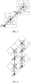
- pixels that can be output by charge adding or signal averaging via one Vsig_n line are arranged in the vertical direction.
- pixels that can be output by charge adding or signal averaging via one Vsig_n line are not arranged in the vertical direction.
- the layout in Fig. 11A is better than the layout in Fig. 11B for signal processing.
Landscapes
- Engineering & Computer Science (AREA)
- Physics & Mathematics (AREA)
- Power Engineering (AREA)
- Electromagnetism (AREA)
- Condensed Matter Physics & Semiconductors (AREA)
- General Physics & Mathematics (AREA)
- Computer Hardware Design (AREA)
- Microelectronics & Electronic Packaging (AREA)
- Multimedia (AREA)
- Signal Processing (AREA)
- Solid State Image Pick-Up Elements (AREA)
- Transforming Light Signals Into Electric Signals (AREA)
Applications Claiming Priority (1)
| Application Number | Priority Date | Filing Date | Title |
|---|---|---|---|
| PCT/CN2016/102195 WO2018068322A1 (en) | 2016-10-14 | 2016-10-14 | Cmos image sensor |
Publications (3)
| Publication Number | Publication Date |
|---|---|
| EP3516691A4 EP3516691A4 (en) | 2019-07-31 |
| EP3516691A1 EP3516691A1 (en) | 2019-07-31 |
| EP3516691B1 true EP3516691B1 (en) | 2021-09-22 |
Family
ID=61904940
Family Applications (1)
| Application Number | Title | Priority Date | Filing Date |
|---|---|---|---|
| EP16918858.8A Active EP3516691B1 (en) | 2016-10-14 | 2016-10-14 | Cmos image sensor |
Country Status (4)
| Country | Link |
|---|---|
| US (1) | US10910429B2 (zh) |
| EP (1) | EP3516691B1 (zh) |
| CN (1) | CN110192281B (zh) |
| WO (1) | WO2018068322A1 (zh) |
Families Citing this family (2)
| Publication number | Priority date | Publication date | Assignee | Title |
|---|---|---|---|---|
| JP5999750B2 (ja) * | 2011-08-25 | 2016-09-28 | ソニー株式会社 | 撮像素子、撮像装置及び生体撮像装置 |
| WO2024007298A1 (en) * | 2022-07-08 | 2024-01-11 | Huawei Technologies Co., Ltd. | Pixel structure, imaging device and electronic device |
Family Cites Families (19)
| Publication number | Priority date | Publication date | Assignee | Title |
|---|---|---|---|---|
| JP3724882B2 (ja) * | 1996-08-14 | 2005-12-07 | シャープ株式会社 | カラー固体撮像装置 |
| US6822682B1 (en) * | 1999-08-18 | 2004-11-23 | Fuji Photo Film Co., Ltd. | Solid state image pickup device and its read method |
| JP2003007995A (ja) | 2001-06-20 | 2003-01-10 | Iwate Toshiba Electronics Co Ltd | Cmosイメージセンサ |
| US7834927B2 (en) * | 2001-08-22 | 2010-11-16 | Florida Atlantic University | Apparatus and method for producing video signals |
| JP4086798B2 (ja) | 2004-02-25 | 2008-05-14 | シャープ株式会社 | 増幅型固体撮像装置 |
| JP4492250B2 (ja) | 2004-08-11 | 2010-06-30 | ソニー株式会社 | 固体撮像素子 |
| US7570290B2 (en) * | 2004-12-27 | 2009-08-04 | Sony Corporation | Drive method for solid-state imaging device, solid-state imaging device, and imaging apparatus |
| CN100444620C (zh) * | 2004-12-27 | 2008-12-17 | 索尼株式会社 | 固态成像装置驱动方法、固态成像装置以及成像设备 |
| JP4389865B2 (ja) * | 2005-11-17 | 2009-12-24 | ソニー株式会社 | 固体撮像素子の信号処理装置および信号処理方法並びに撮像装置 |
| JP4961748B2 (ja) | 2006-01-13 | 2012-06-27 | ソニー株式会社 | 固体撮像装置 |
| JP5292787B2 (ja) | 2007-11-30 | 2013-09-18 | ソニー株式会社 | 固体撮像装置及びカメラ |
| JP5029624B2 (ja) | 2009-01-15 | 2012-09-19 | ソニー株式会社 | 固体撮像装置及び電子機器 |
| US8350940B2 (en) | 2009-06-08 | 2013-01-08 | Aptina Imaging Corporation | Image sensors and color filter arrays for charge summing and interlaced readout modes |
| JP4881987B2 (ja) | 2009-10-06 | 2012-02-22 | キヤノン株式会社 | 固体撮像装置および撮像装置 |
| JP2012124729A (ja) * | 2010-12-09 | 2012-06-28 | Sony Corp | 撮像素子および撮像装置 |
| US9165959B2 (en) * | 2013-02-25 | 2015-10-20 | Omnivision Technologies, Inc. | Image sensor with pixel units having mirrored transistor layout |
| JP6334203B2 (ja) | 2014-02-28 | 2018-05-30 | ソニー株式会社 | 固体撮像装置、および電子機器 |
| KR20150146308A (ko) * | 2014-06-23 | 2015-12-31 | 삼성전자주식회사 | 이미지 센서 및 이미지 센서의 동작 방법 |
| US20180048836A1 (en) * | 2015-03-18 | 2018-02-15 | Sony Corporation | Solid-state imaging device, driving method, and electronic apparatus |
-
2016
- 2016-10-14 EP EP16918858.8A patent/EP3516691B1/en active Active
- 2016-10-14 CN CN201680090042.6A patent/CN110192281B/zh active Active
- 2016-10-14 US US16/341,482 patent/US10910429B2/en active Active
- 2016-10-14 WO PCT/CN2016/102195 patent/WO2018068322A1/en unknown
Also Published As
| Publication number | Publication date |
|---|---|
| CN110192281A (zh) | 2019-08-30 |
| EP3516691A4 (en) | 2019-07-31 |
| WO2018068322A1 (en) | 2018-04-19 |
| CN110192281B (zh) | 2022-06-14 |
| US10910429B2 (en) | 2021-02-02 |
| US20190305029A1 (en) | 2019-10-03 |
| EP3516691A1 (en) | 2019-07-31 |
Similar Documents
| Publication | Publication Date | Title |
|---|---|---|
| KR102614792B1 (ko) | 반도체 장치 및 전자 기기 | |
| JP4457325B2 (ja) | 固体撮像装置 | |
| JP6308760B2 (ja) | 光電変換装置および光電変換装置を有する撮像装置 | |
| US9143760B2 (en) | Solid-state imaging device | |
| US10177192B2 (en) | Image sensor having photodiodes sharing one color filter and one micro-lens | |
| JP6188281B2 (ja) | 光電変換装置 | |
| JP5994344B2 (ja) | 固体撮像装置、電子機器 | |
| US9106856B2 (en) | Solid-state imaging device and imaging apparatus | |
| JP2013510424A (ja) | イメージセンサーのための最適化された光導波路アレイ | |
| WO2014002366A1 (ja) | 固体撮像装置 | |
| US20200075644A1 (en) | Solid-state imaging device | |
| EP3516691B1 (en) | Cmos image sensor | |
| US20210152767A1 (en) | Column-interleaved pixel array | |
| US20220028918A1 (en) | Imaging device | |
| US11031430B2 (en) | Image sensor with dummy lines for minimizing fixed pattern noise (FPN) and electronic apparatus including the same | |
| US10163961B2 (en) | Image sensor | |
| KR102617430B1 (ko) | 이미지 센서 | |
| US11195871B2 (en) | Image sensing device | |
| US20220014700A1 (en) | Imaging device | |
| JP6392542B2 (ja) | 固体撮像装置 | |
| US20220217294A1 (en) | Imaging device | |
| WO2018152819A1 (en) | Cmos image sensor with dual sensitivity pixel |
Legal Events
| Date | Code | Title | Description |
|---|---|---|---|
| STAA | Information on the status of an ep patent application or granted ep patent |
Free format text: STATUS: THE INTERNATIONAL PUBLICATION HAS BEEN MADE |
|
| PUAI | Public reference made under article 153(3) epc to a published international application that has entered the european phase |
Free format text: ORIGINAL CODE: 0009012 |
|
| STAA | Information on the status of an ep patent application or granted ep patent |
Free format text: STATUS: REQUEST FOR EXAMINATION WAS MADE |
|
| 17P | Request for examination filed |
Effective date: 20190423 |
|
| A4 | Supplementary search report drawn up and despatched |
Effective date: 20190603 |
|
| AK | Designated contracting states |
Kind code of ref document: A1 Designated state(s): AL AT BE BG CH CY CZ DE DK EE ES FI FR GB GR HR HU IE IS IT LI LT LU LV MC MK MT NL NO PL PT RO RS SE SI SK SM TR |
|
| AX | Request for extension of the european patent |
Extension state: BA ME |
|
| DAV | Request for validation of the european patent (deleted) | ||
| DAX | Request for extension of the european patent (deleted) | ||
| STAA | Information on the status of an ep patent application or granted ep patent |
Free format text: STATUS: EXAMINATION IS IN PROGRESS |
|
| 17Q | First examination report despatched |
Effective date: 20200709 |
|
| STAA | Information on the status of an ep patent application or granted ep patent |
Free format text: STATUS: EXAMINATION IS IN PROGRESS |
|
| GRAP | Despatch of communication of intention to grant a patent |
Free format text: ORIGINAL CODE: EPIDOSNIGR1 |
|
| STAA | Information on the status of an ep patent application or granted ep patent |
Free format text: STATUS: GRANT OF PATENT IS INTENDED |
|
| INTG | Intention to grant announced |
Effective date: 20210520 |
|
| GRAS | Grant fee paid |
Free format text: ORIGINAL CODE: EPIDOSNIGR3 |
|
| GRAA | (expected) grant |
Free format text: ORIGINAL CODE: 0009210 |
|
| STAA | Information on the status of an ep patent application or granted ep patent |
Free format text: STATUS: THE PATENT HAS BEEN GRANTED |
|
| AK | Designated contracting states |
Kind code of ref document: B1 Designated state(s): AL AT BE BG CH CY CZ DE DK EE ES FI FR GB GR HR HU IE IS IT LI LT LU LV MC MK MT NL NO PL PT RO RS SE SI SK SM TR |
|
| REG | Reference to a national code |
Ref country code: GB Ref legal event code: FG4D |
|
| REG | Reference to a national code |
Ref country code: DE Ref legal event code: R096 Ref document number: 602016064188 Country of ref document: DE |
|
| REG | Reference to a national code |
Ref country code: IE Ref legal event code: FG4D |
|
| REG | Reference to a national code |
Ref country code: CH Ref legal event code: EP Ref country code: AT Ref legal event code: REF Ref document number: 1432978 Country of ref document: AT Kind code of ref document: T Effective date: 20211015 |
|
| REG | Reference to a national code |
Ref country code: LT Ref legal event code: MG9D |
|
| REG | Reference to a national code |
Ref country code: NL Ref legal event code: MP Effective date: 20210922 |
|
| PG25 | Lapsed in a contracting state [announced via postgrant information from national office to epo] |
Ref country code: RS Free format text: LAPSE BECAUSE OF FAILURE TO SUBMIT A TRANSLATION OF THE DESCRIPTION OR TO PAY THE FEE WITHIN THE PRESCRIBED TIME-LIMIT Effective date: 20210922 Ref country code: SE Free format text: LAPSE BECAUSE OF FAILURE TO SUBMIT A TRANSLATION OF THE DESCRIPTION OR TO PAY THE FEE WITHIN THE PRESCRIBED TIME-LIMIT Effective date: 20210922 Ref country code: LT Free format text: LAPSE BECAUSE OF FAILURE TO SUBMIT A TRANSLATION OF THE DESCRIPTION OR TO PAY THE FEE WITHIN THE PRESCRIBED TIME-LIMIT Effective date: 20210922 Ref country code: BG Free format text: LAPSE BECAUSE OF FAILURE TO SUBMIT A TRANSLATION OF THE DESCRIPTION OR TO PAY THE FEE WITHIN THE PRESCRIBED TIME-LIMIT Effective date: 20211222 Ref country code: NO Free format text: LAPSE BECAUSE OF FAILURE TO SUBMIT A TRANSLATION OF THE DESCRIPTION OR TO PAY THE FEE WITHIN THE PRESCRIBED TIME-LIMIT Effective date: 20211222 Ref country code: HR Free format text: LAPSE BECAUSE OF FAILURE TO SUBMIT A TRANSLATION OF THE DESCRIPTION OR TO PAY THE FEE WITHIN THE PRESCRIBED TIME-LIMIT Effective date: 20210922 Ref country code: FI Free format text: LAPSE BECAUSE OF FAILURE TO SUBMIT A TRANSLATION OF THE DESCRIPTION OR TO PAY THE FEE WITHIN THE PRESCRIBED TIME-LIMIT Effective date: 20210922 |
|
| REG | Reference to a national code |
Ref country code: AT Ref legal event code: MK05 Ref document number: 1432978 Country of ref document: AT Kind code of ref document: T Effective date: 20210922 |
|
| PG25 | Lapsed in a contracting state [announced via postgrant information from national office to epo] |
Ref country code: LV Free format text: LAPSE BECAUSE OF FAILURE TO SUBMIT A TRANSLATION OF THE DESCRIPTION OR TO PAY THE FEE WITHIN THE PRESCRIBED TIME-LIMIT Effective date: 20210922 Ref country code: GR Free format text: LAPSE BECAUSE OF FAILURE TO SUBMIT A TRANSLATION OF THE DESCRIPTION OR TO PAY THE FEE WITHIN THE PRESCRIBED TIME-LIMIT Effective date: 20211223 |
|
| PG25 | Lapsed in a contracting state [announced via postgrant information from national office to epo] |
Ref country code: AT Free format text: LAPSE BECAUSE OF FAILURE TO SUBMIT A TRANSLATION OF THE DESCRIPTION OR TO PAY THE FEE WITHIN THE PRESCRIBED TIME-LIMIT Effective date: 20210922 |
|
| REG | Reference to a national code |
Ref country code: CH Ref legal event code: PL |
|
| PG25 | Lapsed in a contracting state [announced via postgrant information from national office to epo] |
Ref country code: IS Free format text: LAPSE BECAUSE OF FAILURE TO SUBMIT A TRANSLATION OF THE DESCRIPTION OR TO PAY THE FEE WITHIN THE PRESCRIBED TIME-LIMIT Effective date: 20220122 Ref country code: SK Free format text: LAPSE BECAUSE OF FAILURE TO SUBMIT A TRANSLATION OF THE DESCRIPTION OR TO PAY THE FEE WITHIN THE PRESCRIBED TIME-LIMIT Effective date: 20210922 Ref country code: RO Free format text: LAPSE BECAUSE OF FAILURE TO SUBMIT A TRANSLATION OF THE DESCRIPTION OR TO PAY THE FEE WITHIN THE PRESCRIBED TIME-LIMIT Effective date: 20210922 Ref country code: PT Free format text: LAPSE BECAUSE OF FAILURE TO SUBMIT A TRANSLATION OF THE DESCRIPTION OR TO PAY THE FEE WITHIN THE PRESCRIBED TIME-LIMIT Effective date: 20220124 Ref country code: PL Free format text: LAPSE BECAUSE OF FAILURE TO SUBMIT A TRANSLATION OF THE DESCRIPTION OR TO PAY THE FEE WITHIN THE PRESCRIBED TIME-LIMIT Effective date: 20210922 Ref country code: NL Free format text: LAPSE BECAUSE OF FAILURE TO SUBMIT A TRANSLATION OF THE DESCRIPTION OR TO PAY THE FEE WITHIN THE PRESCRIBED TIME-LIMIT Effective date: 20210922 Ref country code: ES Free format text: LAPSE BECAUSE OF FAILURE TO SUBMIT A TRANSLATION OF THE DESCRIPTION OR TO PAY THE FEE WITHIN THE PRESCRIBED TIME-LIMIT Effective date: 20210922 Ref country code: EE Free format text: LAPSE BECAUSE OF FAILURE TO SUBMIT A TRANSLATION OF THE DESCRIPTION OR TO PAY THE FEE WITHIN THE PRESCRIBED TIME-LIMIT Effective date: 20210922 Ref country code: CZ Free format text: LAPSE BECAUSE OF FAILURE TO SUBMIT A TRANSLATION OF THE DESCRIPTION OR TO PAY THE FEE WITHIN THE PRESCRIBED TIME-LIMIT Effective date: 20210922 Ref country code: AL Free format text: LAPSE BECAUSE OF FAILURE TO SUBMIT A TRANSLATION OF THE DESCRIPTION OR TO PAY THE FEE WITHIN THE PRESCRIBED TIME-LIMIT Effective date: 20210922 |
|
| REG | Reference to a national code |
Ref country code: DE Ref legal event code: R097 Ref document number: 602016064188 Country of ref document: DE Ref country code: BE Ref legal event code: MM Effective date: 20211031 |
|
| PG25 | Lapsed in a contracting state [announced via postgrant information from national office to epo] |
Ref country code: MC Free format text: LAPSE BECAUSE OF FAILURE TO SUBMIT A TRANSLATION OF THE DESCRIPTION OR TO PAY THE FEE WITHIN THE PRESCRIBED TIME-LIMIT Effective date: 20210922 |
|
| PG25 | Lapsed in a contracting state [announced via postgrant information from national office to epo] |
Ref country code: LU Free format text: LAPSE BECAUSE OF NON-PAYMENT OF DUE FEES Effective date: 20211014 Ref country code: DK Free format text: LAPSE BECAUSE OF FAILURE TO SUBMIT A TRANSLATION OF THE DESCRIPTION OR TO PAY THE FEE WITHIN THE PRESCRIBED TIME-LIMIT Effective date: 20210922 Ref country code: BE Free format text: LAPSE BECAUSE OF NON-PAYMENT OF DUE FEES Effective date: 20211031 |
|
| PLBE | No opposition filed within time limit |
Free format text: ORIGINAL CODE: 0009261 |
|
| STAA | Information on the status of an ep patent application or granted ep patent |
Free format text: STATUS: NO OPPOSITION FILED WITHIN TIME LIMIT |
|
| 26N | No opposition filed |
Effective date: 20220623 |
|
| PG25 | Lapsed in a contracting state [announced via postgrant information from national office to epo] |
Ref country code: LI Free format text: LAPSE BECAUSE OF NON-PAYMENT OF DUE FEES Effective date: 20211031 Ref country code: CH Free format text: LAPSE BECAUSE OF NON-PAYMENT OF DUE FEES Effective date: 20211031 |
|
| PG25 | Lapsed in a contracting state [announced via postgrant information from national office to epo] |
Ref country code: IE Free format text: LAPSE BECAUSE OF NON-PAYMENT OF DUE FEES Effective date: 20211014 |
|
| PG25 | Lapsed in a contracting state [announced via postgrant information from national office to epo] |
Ref country code: SI Free format text: LAPSE BECAUSE OF FAILURE TO SUBMIT A TRANSLATION OF THE DESCRIPTION OR TO PAY THE FEE WITHIN THE PRESCRIBED TIME-LIMIT Effective date: 20210922 Ref country code: FR Free format text: LAPSE BECAUSE OF NON-PAYMENT OF DUE FEES Effective date: 20211122 |
|
| PG25 | Lapsed in a contracting state [announced via postgrant information from national office to epo] |
Ref country code: IT Free format text: LAPSE BECAUSE OF FAILURE TO SUBMIT A TRANSLATION OF THE DESCRIPTION OR TO PAY THE FEE WITHIN THE PRESCRIBED TIME-LIMIT Effective date: 20210922 |
|
| PG25 | Lapsed in a contracting state [announced via postgrant information from national office to epo] |
Ref country code: CY Free format text: LAPSE BECAUSE OF FAILURE TO SUBMIT A TRANSLATION OF THE DESCRIPTION OR TO PAY THE FEE WITHIN THE PRESCRIBED TIME-LIMIT Effective date: 20210922 |
|
| PG25 | Lapsed in a contracting state [announced via postgrant information from national office to epo] |
Ref country code: SM Free format text: LAPSE BECAUSE OF FAILURE TO SUBMIT A TRANSLATION OF THE DESCRIPTION OR TO PAY THE FEE WITHIN THE PRESCRIBED TIME-LIMIT Effective date: 20210922 Ref country code: HU Free format text: LAPSE BECAUSE OF FAILURE TO SUBMIT A TRANSLATION OF THE DESCRIPTION OR TO PAY THE FEE WITHIN THE PRESCRIBED TIME-LIMIT; INVALID AB INITIO Effective date: 20161014 |
|
| PGFP | Annual fee paid to national office [announced via postgrant information from national office to epo] |
Ref country code: GB Payment date: 20230831 Year of fee payment: 8 |
|
| PGFP | Annual fee paid to national office [announced via postgrant information from national office to epo] |
Ref country code: DE Payment date: 20230830 Year of fee payment: 8 |
|
| PG25 | Lapsed in a contracting state [announced via postgrant information from national office to epo] |
Ref country code: MK Free format text: LAPSE BECAUSE OF FAILURE TO SUBMIT A TRANSLATION OF THE DESCRIPTION OR TO PAY THE FEE WITHIN THE PRESCRIBED TIME-LIMIT Effective date: 20210922 |