EP3507826B1 - Bonded wafer metrology - Google Patents
Bonded wafer metrology Download PDFInfo
- Publication number
- EP3507826B1 EP3507826B1 EP17876339.7A EP17876339A EP3507826B1 EP 3507826 B1 EP3507826 B1 EP 3507826B1 EP 17876339 A EP17876339 A EP 17876339A EP 3507826 B1 EP3507826 B1 EP 3507826B1
- Authority
- EP
- European Patent Office
- Prior art keywords
- wafer
- edge profile
- profile images
- vertical line
- images
- Prior art date
- Legal status (The legal status is an assumption and is not a legal conclusion. Google has not performed a legal analysis and makes no representation as to the accuracy of the status listed.)
- Active
Links
Images


Classifications
-
- G—PHYSICS
- G06—COMPUTING OR CALCULATING; COUNTING
- G06T—IMAGE DATA PROCESSING OR GENERATION, IN GENERAL
- G06T7/00—Image analysis
- G06T7/0002—Inspection of images, e.g. flaw detection
- G06T7/0004—Industrial image inspection
-
- H—ELECTRICITY
- H10—SEMICONDUCTOR DEVICES; ELECTRIC SOLID-STATE DEVICES NOT OTHERWISE PROVIDED FOR
- H10P—GENERIC PROCESSES OR APPARATUS FOR THE MANUFACTURE OR TREATMENT OF DEVICES COVERED BY CLASS H10
- H10P74/00—Testing or measuring during manufacture or treatment of wafers, substrates or devices
- H10P74/27—Structural arrangements therefor
-
- G—PHYSICS
- G01—MEASURING; TESTING
- G01B—MEASURING LENGTH, THICKNESS OR SIMILAR LINEAR DIMENSIONS; MEASURING ANGLES; MEASURING AREAS; MEASURING IRREGULARITIES OF SURFACES OR CONTOURS
- G01B11/00—Measuring arrangements characterised by the use of optical techniques
- G01B11/002—Measuring arrangements characterised by the use of optical techniques for measuring two or more coordinates
-
- G—PHYSICS
- G01—MEASURING; TESTING
- G01B—MEASURING LENGTH, THICKNESS OR SIMILAR LINEAR DIMENSIONS; MEASURING ANGLES; MEASURING AREAS; MEASURING IRREGULARITIES OF SURFACES OR CONTOURS
- G01B11/00—Measuring arrangements characterised by the use of optical techniques
- G01B11/24—Measuring arrangements characterised by the use of optical techniques for measuring contours or curvatures
- G01B11/2433—Measuring arrangements characterised by the use of optical techniques for measuring contours or curvatures for measuring outlines by shadow casting
-
- G—PHYSICS
- G06—COMPUTING OR CALCULATING; COUNTING
- G06T—IMAGE DATA PROCESSING OR GENERATION, IN GENERAL
- G06T7/00—Image analysis
- G06T7/10—Segmentation; Edge detection
- G06T7/13—Edge detection
-
- G—PHYSICS
- G06—COMPUTING OR CALCULATING; COUNTING
- G06T—IMAGE DATA PROCESSING OR GENERATION, IN GENERAL
- G06T7/00—Image analysis
- G06T7/60—Analysis of geometric attributes
-
- G—PHYSICS
- G06—COMPUTING OR CALCULATING; COUNTING
- G06T—IMAGE DATA PROCESSING OR GENERATION, IN GENERAL
- G06T7/00—Image analysis
- G06T7/70—Determining position or orientation of objects or cameras
- G06T7/73—Determining position or orientation of objects or cameras using feature-based methods
-
- H—ELECTRICITY
- H10—SEMICONDUCTOR DEVICES; ELECTRIC SOLID-STATE DEVICES NOT OTHERWISE PROVIDED FOR
- H10P—GENERIC PROCESSES OR APPARATUS FOR THE MANUFACTURE OR TREATMENT OF DEVICES COVERED BY CLASS H10
- H10P74/00—Testing or measuring during manufacture or treatment of wafers, substrates or devices
- H10P74/20—Testing or measuring during manufacture or treatment of wafers, substrates or devices characterised by the properties tested or measured, e.g. structural or electrical properties
- H10P74/203—Structural properties, e.g. testing or measuring thicknesses, line widths, warpage, bond strengths or physical defects
-
- H—ELECTRICITY
- H10—SEMICONDUCTOR DEVICES; ELECTRIC SOLID-STATE DEVICES NOT OTHERWISE PROVIDED FOR
- H10P—GENERIC PROCESSES OR APPARATUS FOR THE MANUFACTURE OR TREATMENT OF DEVICES COVERED BY CLASS H10
- H10P74/00—Testing or measuring during manufacture or treatment of wafers, substrates or devices
- H10P74/23—Testing or measuring during manufacture or treatment of wafers, substrates or devices characterised by multiple measurements, corrections, marking or sorting processes
- H10P74/235—Testing or measuring during manufacture or treatment of wafers, substrates or devices characterised by multiple measurements, corrections, marking or sorting processes comprising optical enhancement of defects or not-directly-visible states
-
- G—PHYSICS
- G01—MEASURING; TESTING
- G01B—MEASURING LENGTH, THICKNESS OR SIMILAR LINEAR DIMENSIONS; MEASURING ANGLES; MEASURING AREAS; MEASURING IRREGULARITIES OF SURFACES OR CONTOURS
- G01B2210/00—Aspects not specifically covered by any group under G01B, e.g. of wheel alignment, caliper-like sensors
- G01B2210/56—Measuring geometric parameters of semiconductor structures, e.g. profile, critical dimensions or trench depth
-
- G—PHYSICS
- G06—COMPUTING OR CALCULATING; COUNTING
- G06T—IMAGE DATA PROCESSING OR GENERATION, IN GENERAL
- G06T2207/00—Indexing scheme for image analysis or image enhancement
- G06T2207/20—Special algorithmic details
- G06T2207/20048—Transform domain processing
- G06T2207/20061—Hough transform
-
- G—PHYSICS
- G06—COMPUTING OR CALCULATING; COUNTING
- G06T—IMAGE DATA PROCESSING OR GENERATION, IN GENERAL
- G06T2207/00—Indexing scheme for image analysis or image enhancement
- G06T2207/30—Subject of image; Context of image processing
- G06T2207/30108—Industrial image inspection
- G06T2207/30148—Semiconductor; IC; Wafer
-
- H—ELECTRICITY
- H10—SEMICONDUCTOR DEVICES; ELECTRIC SOLID-STATE DEVICES NOT OTHERWISE PROVIDED FOR
- H10P—GENERIC PROCESSES OR APPARATUS FOR THE MANUFACTURE OR TREATMENT OF DEVICES COVERED BY CLASS H10
- H10P52/00—Grinding, lapping or polishing of wafers, substrates or parts of devices
- H10P52/40—Chemomechanical polishing [CMP]
- H10P52/402—Chemomechanical polishing [CMP] of semiconductor materials
-
- H—ELECTRICITY
- H10—SEMICONDUCTOR DEVICES; ELECTRIC SOLID-STATE DEVICES NOT OTHERWISE PROVIDED FOR
- H10P—GENERIC PROCESSES OR APPARATUS FOR THE MANUFACTURE OR TREATMENT OF DEVICES COVERED BY CLASS H10
- H10P74/00—Testing or measuring during manufacture or treatment of wafers, substrates or devices
- H10P74/23—Testing or measuring during manufacture or treatment of wafers, substrates or devices characterised by multiple measurements, corrections, marking or sorting processes
Definitions
- This disclosure relates to wafer metrology.
- Fabricating semiconductor devices typically includes processing a substrate like a semiconductor wafer using a large number of semiconductor fabrication processes to form various features and multiple levels of the semiconductor devices.
- lithography is a semiconductor fabrication process that involves transferring a pattern from a reticle to a resist arranged on a semiconductor wafer. Additional examples of semiconductor fabrication processes include, but are not limited to, chemical-mechanical polishing (CMP), etch, deposition, and ion implantation.
- CMP chemical-mechanical polishing
- etch etch
- deposition deposition
- ion implantation ion implantation
- Bonded (or stacked) wafers are frequently used in the semiconductor industry.
- One or more ultrathin wafers bonded to a carrier wafer is an example of a bonded wafer, though other semiconductor wafer designs also can be bonded wafers.
- a bonded wafer can include a top wafer (e.g., a device wafer) bonded to a carrier wafer. These bonded wafers can be used for both memory and logic applications.
- Three-dimensional integrated circuits (3D IC) can be produced using bonded wafers.
- Bonded wafers can have complex edge profiles.
- the various layers of a bonded wafer can have different heights and diameters. These dimensions can be affected by the size of the various wafers prior to stacking or by processing steps.
- Bonded wafers with fabrication errors can cause problems during manufacturing. For example, centricity of the bonded wafer affects the CMP process or increases handling risks. During CMP, centricity affects placement of the polishing pad with respect to the center of the bonded wafer and subsequent planarization. During wafer handling, the balance of a bonded wafer or clearance within manufacturing equipment can be affected by centricity of the bonded wafer.
- Improper centricity can even ruin a bonded wafer or damage manufacturing equipment. If the bonded wafer is undercut, improperly bonded together, or contains too much glue, then the bonded wafer can break within the CMP tool, contaminating or damaging the CMP tool. Such contamination or damage leads to unwanted downtime or can even stop production within a semiconductor fab.
- a CMP process on a bonded wafer with improper centricity can result in undesired edge profiles on the bonded wafer. For example, too much or not enough material may be removed during a CMP process or the CMP process may result in undercuts, overhangs, or whiskers. These undesired edge profiles can affect device yield or can impact later manufacturing steps.
- US2013139950 discloses a rotational misalignment measuring device of bonded substrate, rotational misalignment measuring method of bonded substrate, and method of manufacturing bonded substrate.
- a metrology system as recited in claim 1 is provided in a first embodiment.
- a non-transitory computer readable medium storing a program as recited in claim 10 is provided.
- semiconductor wafers can be stacked and bonded together.
- At least one top wafer which may be a device wafer or some other type of wafer, is placed on a carrier wafer.
- the top wafer and the carrier wafer can be connected by an adhesive material.
- Several process parameters such as an amount of adhesive, force, temperature, wafer shape, and placement accuracy may cause a wafer displacement between the top wafer and the carrier wafer, such as the carrier wafer and the top wafer not being centered relative to each other.
- Methods and systems to measure wafer-to-wafer displacement of two or more wafers (e.g., top wafer and carrier wafer) in a bonded wafer are disclosed. For example, displacement in the X and Y dimensions can be determined. The X, Y, and Z coordinates of the wafer edge can be used to determine the center of each of the bonded wafers.
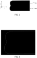
- FIG. 1 is an exemplary wafer edge profile image of a circumferential edge of a bonded wafer having a carrier wafer 300 and a top wafer 301.
- FIG. 1 is an example of a shadowgram image. From the edge contour and the wafer rotation angle, the X, Y, and Z coordinates of the wafer edge are extracted with Z being the thickness of the wafers in the bonded wafer. From these coordinates, the center of each of the bonded wafers can be determined.
- image processing techniques are used to isolate vertically-connected pixels along the contour of the edge profiler image. Based on user-defined zones and slope tolerance parameters, vertically connected pixels (e.g., vertical line segments) are grouped into two regions. One region is associated with the top wafer and the other region is associated with the carrier wafer. Average X distances of these line segments can then be calculated from the edge of the image frame or some other reference point for the two groups. Absolute offset is calculated as difference between these average values. This is repeated for all wafer edge profile images acquired around the wafer (e.g., every 10 degrees around the circumference of the bonded wafer) to generate an offset curve. A model is then applied to calculate the X and Y offsets between the top wafer and the carrier wafer from this curve.
- vertically connected pixels e.g., vertical line segments
- FIG. 2 is a contour extracted from the wafer edge profile image of FIG. 1 .
- the wafer edge profile image of FIG. 1 may be sharpened or otherwise cleaned up prior to extraction, such as to remove scale bars. Scale bars may be removed by, for example, cropping the image.
- Other pre-processing such as fringe removal, noise filtering, or color depth reduction down to two bit (black and white), also may be performed.
- the contour of the edge profile in FIG. 2 may be extracted, such as by using a high pass filter.
- a canny edge extraction method is used during which some smoothing may be performed to avoid noisy edges in the images.
- Other smoothing may be performed during edge extraction depending on the edge extraction algorithm.
- FIG. 3 illustrates vertical line segments of the contour shown in FIG. 2 after grouping.
- the line segments can be grouped into regions associated with the top wafer and the carrier wafer.
- the vertical line segments represent or approximate an extent of the wafer and are circled in FIG. 3 with a dotted line.
- X top is an average X distance of the top line segments (e.g., the top wafer)
- X bot is an average X distance of the bottom line segments (e.g., the carrier wafer).
- X top and X bot can be, for example, an average distance from the edge of an image frame or other reference. For example, this may be an average distance with respect to left hand side of image frame. The actual average or reference point for the two averages may not matter because a difference between two averages is used.
- a Hough Transform based technique, local slope calculation, or other techniques known in the art may be used to determine vertical line segments on the edge contour.
- the local slope calculation is based on a few pixels and only those pixels are selected whose local slope indicates a vertical edge.
- An offset between the two vertical line segments is then calculated. For example, an average X distance from the edge of image frame for lines in each group is calculated based on FIG. 3 . A total offset as difference between these two average values is also calculated based on FIG. 3 .
- FIGs. 2 and 3 can be repeated for all wafer edge profile images (e.g., every 10 degrees around the circumference of the bonded wafer) and an offset curve is generated.
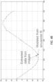
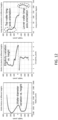
- An exemplary offset curve is illustrated in FIGs. 4A and 4B.
- FIG. 4B also illustrates the data being modelled from a sinusoidal fit.
- a sinusoidal model can be applied to calculate X and Y offsets from the total offset curve.
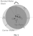
- FIG. 5 A cos ( ⁇ - ⁇ ) + C.
- A, ⁇ , and C are the unknowns.
- ⁇ is measured with respect to horizontal axis
- ⁇ is an angle between a line joining two centers and a horizontal axis
- C1 is the center of the top wafer
- C2 is the center of the carrier wafer
- A is the distance between the centers of the two wafers
- X is the X offset between the two wafers
- Y is the Y offset between the two wafers.
- the pixel size may be, for example, 2.408 ⁇ m, though other sizes are possible.
- Input parameters for this embodiment that isolates vertically-connected pixels can include slope tolerance and zone.
- slope tolerance a user can set how much tolerance is allowed from a perfect vertical line.
- zone a user can define top and bottom wafer zones for accurate computation during grouping.
- any wafer-to-stage placement error does not impact computations involved in isolating vertically-connected pixels.
- any wafer placement on a stage may be acceptable.
- This measurement also is free from any shift in the image coordinate space due to calibration drifts because the difference between two averages is calculated to have the offset curve. Thus, the difference will not be impacted even if the individual averages change because of the drift.
- the embodiment of FIGs. 2-5 may include a step to remove messy edges or artifacts. This may occur prior to finding the vertical line segments.
- a wafer edge profile image with messy edges or artifacts can be skipped and other wafer edge profile images of a wafer can be relied upon instead.
- a model-based approach is used.
- the contour coordinates of the edge profile images are extracted.
- the coordinates for wafer bevel and apex are then used to fit an elliptical model.
- FIG. 6 includes an exemplary wafer edge profile image of a circumferential edge of a wafer on the left and extracted edge contour coordinates from the wafer edge profile image on the right.
- Edge coordinates can be extracted from the wafer edge profile image using, for example, a high pass filter. Stage effects can be corrected. Coordinates of points at the bevel and apex (circled with the dotted line in FIG. 6 ) can be saved or otherwise noted. This process can be repeated for all wafer edge profile images for a wafer (e.g., every 10 degrees around the circumference of the bonded wafer). At least three images may be needed to provide the relative center offset, but more images can proved higher accuracy in terms of reduce roughness at the edge or the circularity error. For example, 36 images may be taken.
- FIG. 7 illustrates an algorithm analyzing the wafer edge profile image of FIG. 6 slice by slice.
- the coordinates are fitted to an elliptical model, such as that illustrated in FIG. 8 , on a slice-by-slice basis.
- CoR is the center of rotation
- CoW is the center of the wafer. This results in a center of wafer per slice, as shown in FIGs. 9-10 .
- a typical step size may be 2.5 microns.
- Its coordinate can be the orientation ( ⁇ ) and radius, shown as solid line in FIG. 9 .
- the parameters of the model include CoR and CoW currently set as the reference.
- the wafer circularity is modeled as an ellipse with its long axis R+ ⁇ , and short axis R- ⁇ .
- the position of images is calculated, shown as dots in FIG. 9 .
- a non-linear regression algorithm can be used to adjust the hypotheses model parameters so that the model prediction (dots in FIG. 9 ) is best matched with the measured value (solid line in FIG. 9 ).
- the model parameters that give best match are reported as the measurement results, in terms of CoR, wafer radius, wafer ellipticity as shown in FIG. 8 .
- the center positions of the wafers are calculated from the results of the slices.
- the calculated center positions are sorted into N sets where N is the number of wafers in a bonded wafer (i.e., N>1).
- the sorting may be done using knowledge of wafer thicknesses and/or filtering. Filtering can include deviation from median and/or knowledge about the height location.
- the center positions of each wafer can be calculated for each set corresponding to a wafer by averaging, using a median, or with other techniques.
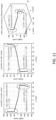
- FIGs. 11-12 illustrate wafer radius and circularity results.
- the calculated wafer centers with respect to the center of rotation in FIG. 11 and FIG. 12 show the wafer radius at different slices and the ellipticity.
- FIGs. 6-12 may use an elliptical model.
- FIG. 2-5 and FIGs. 6-12 can be used separately or in the alternative, both the embodiment of FIGs. 2-5 and the embodiment of FIGs. 6-12 are used together in the present invention.
- the embodiment of FIGs. 6-12 is performed first. Then the embodiment of FIGs. 2-5 may be performed to verify results.
- the embodiment of FIGs. 6-12 may provide more accurate results because its analysis includes more non-ideal factors in the model, may provide more information because detailed edge information is preserved in the analysis process, and may be faster.
- the embodiment of FIGs. 2-5 may be a backup if the embodiment of FIGs. 6-12 is unable to provide acceptable or clear results.
- the wafer edge data/coordinates are acquired using wafer edge profile images.
- a profiler, laser triangulation, or other techniques could be used to generate the inputs instead.
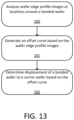
- FIG. 13 is a flowchart of an embodiment of a bonded wafer metrology method.
- wafer edge profile images are analyzed at locations around a bonded wafer, which may have a top wafer and a carrier wafer.
- an offset curved is generated based on the wafer edge profile images.
- displacement of the top wafer to the carrier wafer is determined based on the offset curve.
- the wafer edge profile images may be generated at multiple locations around the wafer prior to the analysis 200.
- the wafer edge profile images may be shadowgram images.
- a carrier wafer and a top wafer are illustrated, more than two wafers may be bonded together. For example, three wafers may be bonded to a carrier wafer. The offset between adjacent wafer, between pairs of wafers, or for the overall bonded wafer can be calculated.
- a first vertical line segment in each of the edge profile images for the top wafer is determined and a second vertical line segment in each of the edge profile images for the carrier wafer is determined.
- a sinusoidal model may be used to determine the displacement.
- edge coordinates are extracted from each of the edge profile images. Coordinates of points at a bevel and an apex in each of the edge profile images are determined. The coordinates are fitted to an elliptical model. A center position of the top wafer and the carrier wafer is calculated. Stage effects can be corrected after the extracting.
- Additional wafer properties can be obtained from the image analysis, such as wafer circularity or other irregularities such as the shape of the individual wafer edges. For example, whether the wafer edge is angled and the direction of the angle can be determined.
- the systems and methods disclosed herein can be used for concurrent wafer edge inspection and edge profiling.
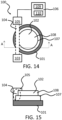
- FIGs. 14-15 are a top view and corresponding cross-sectional side view along A-A of a block diagram of a system 100 in accordance with an embodiment of the present disclosure.
- FIG. 16 is a perspective view of a system 100 corresponding to the embodiment of FIGs. 14-15 .
- System 100 is configured to perform metrology of a bonded wafer by acquiring images that are shadowgrams.
- a shadowgram applies a shadowgraph technique and visualizes or images a shadow of the bonded wafer 102, such as a circumferential edge of the bonded wafer 102.
- a stage 101 can be configured to rotate a bonded wafer 102, though the system 100 also can rotate with respect to the bonded wafer 102. Such rotation can be stepped or continuous.
- the bonded wafer 102 also may not rotate during imaging and components of the system 100 may be fixed.
- the exemplary bonded wafer 102 is shown with a carrier wafer 107 and a top wafer 108.
- the carrier wafer 107 and top wafer 108 may have different diameters, such as those illustrated in FIG. 1 .
- the carrier wafer 107 can be a carrier wafer and the top wafer 108 can be a device wafer.
- the carrier wafer 107 and top wafer 108 can both be device wafers or more than the carrier wafer 107 and top wafer 108 can form the bonded wafer 102.
- a light source 103 is configured to direct collimated light 104 at an edge of the bonded wafer 102.
- the collimated light 104 is directed tangentially, with respect to the bonded wafer 102, so as to create a shadow of the edge profile.
- the bonded wafer 102 blocks some of the collimated light 104.
- the collimated light 104 is illustrated as approximately circular, but can be other shapes.
- the light source 103 utilizes a light-emitting diode (LED).
- LED light-emitting diode
- Other suitable light sources 103 such as a lamp that produces collimated light, laser, supercontinuum laser, laser-driven phosphor, or laser-driven lamp, will be apparent in light of the present disclosure.
- the light source 103 can include both single band and broadband light sources in a single system or multiple systems.
- the collimated light 104 may be parallel to a plane of the bonded wafer 102.
- the collimated light 104 may be parallel to the plane of the carrier wafer 107 on which the top wafer 108 is disposed.
- Diffraction suppression techniques may be used to remove diffraction-related artifacts that may adversely affect measurements. Approximately a few millimeters of the bonded wafer 102 are seen in a profile using the collimated light 104, though other dimensions are possible.
- a detector 105 located apart from the light source 103 receives at least some of the collimated light 104.
- the detector 105 is located such that when a bonded wafer 102 is being imaged, at least a portion of the shadow (i.e., the light producing the shadow) is received by the detector 105.
- the detector 105 can be, for example, a charge-coupled device (CCD) or complementary metal-oxide-semiconductor (CMOS) camera. In this way, an image of the wafer edge silhouette is formed (i.e., a wafer edge profile image).
- the detector 105 can be configured to collect hundreds of wafer edge profile images of the bonded wafer 102 for high sampling.
- wafer edge profile image of the bonded wafer 102 may be collected, though more images can be collected.
- 16 wafer edge profile images of a bonded wafer are collected.
- 36 wafer edge profile images of a bonded wafer are collected.
- 360 wafer edge profile images of a bonded wafer are collected.
- the collimated light 104 may have a wavelength or wavelengths that produce a shadow. For example, visible light such as blue light or white light may be used. Other suitable collimated light 104 will be apparent in light of the present disclosure. For example, ultraviolet light can be used.
- the collimated light 104 may be polarized and may be pulsed or continuous.
- multiple light sources 103 and detectors 105 may be used. Multiple light sources 103 and detectors 105 may be placed at various locations around the perimeter of the bonded wafer 102 to collect images at different locations of the bonded wafer 102. This may increase inspection throughput or increase the number of images produced while minimizing the impact to inspection throughput. If multiple light sources 103 and detectors 105 are placed at various locations around the perimeter of the bonded wafer 102, then the bonded wafer 102 may not rotate with respect to the light source 103 or detector 105.
- a controller 106 is operatively connected to the detector 105.
- the controller 106 is configured to analyze an image of the edge of the bonded wafer 102 and can control the acquisition of the images using the detector 105. For example, the controller 106 can rotate the bonded wafer 102 with respect to the light source 103 or detector 105.
- the controller 106 also can control the timing or locations of image acquisition on the bonded wafer 102.
- the controller 106 may be configured to perform other functions or additional steps using the output of the detector 105. For example, the controller 106 may be programmed to perform some or all of the steps of FIG. 13 .
- the controller 106 can include a processor 109 and a memory 110.
- the controller 106, other system(s), or other subsystem(s) described herein may take various forms, including a personal computer system, workstation, image computer, mainframe computer system, workstation, network appliance, internet appliance, parallel processor, or other device.
- the term "controller” may be broadly defined to encompass any device having one or more processors that executes instructions from a memory medium.
- the subsystem(s) or system(s) may also include any suitable processor known in the art, such as a parallel processor.
- the subsystem(s) or system(s) may include a platform with high speed processing and software, either as a standalone or a networked tool.
- the different subsystems may be coupled to each other such that images, data, information, instructions, etc. can be sent between the subsystems.
- one subsystem may be coupled to additional subsystem(s) by any suitable transmission media, which may include any suitable wired and/or wireless transmission media known in the art.
- Two or more of such subsystems may also be effectively coupled by a shared computer-readable storage medium (not shown).
- the controller 106 may be communicatively coupled to any of the various components or sub-systems of system 100 in any manner known in the art. Moreover, the controller 106 may be configured to receive and/or acquire data or information from other systems by a transmission medium that may include wireline and/or wireless portions. In this manner, the transmission medium may serve as a data link between the controller 106 and other subsystems of the system 100 or systems external to system 100.
- An additional embodiment relates to a non-transitory computer-readable medium storing program instructions executable on a controller for performing a computer-implemented method for bonded wafer metrology, such as for performing the techniques disclosed herein.
- the controller 106 can include a memory 110 or other electronic data storage medium with non-transitory computer-readable medium that includes program instructions executable on the controller 106.
- the computer-implemented method may include any step(s) of any method(s) described herein, such as that disclosed with respect to FIG. 13 .
- the memory 110 or other electronic data storage medium may be a storage medium such as a read-only memory, a random access memory, a magnetic or optical disk, a non-volatile memory, a solid state memory, a magnetic tape, or any other suitable non-transitory computer-readable medium known in the art.
- the program instructions may be implemented in any of various ways, including procedure-based techniques, component-based techniques, and/or object-oriented techniques, among others.
- the program instructions may be implemented using ActiveX controls, C++ objects, JavaBeans, Microsoft Foundation Classes (MFC), SSE (Streaming SIMD Extension), or other technologies or methodologies, as desired.
- MFC Microsoft Foundation Classes
- SSE Streaming SIMD Extension
- various steps, functions, and/or operations of system 100 and the methods disclosed herein are carried out by one or more of the following: electronic circuits, logic gates, multiplexers, programmable logic devices, application-specific integrated circuits (ASICs), analog or digital controls/switches, microcontrollers, or computing systems.
- Program instructions implementing methods such as those described herein may be transmitted over or stored on carrier medium.
- a carrier medium may include an electronic data storage medium, such as that of the memory 110, or a transmission medium such as a wire, cable, or wireless transmission link.
- the various steps described throughout the present disclosure may be carried out by a single controller 106 (or computer system) or, alternatively, multiple controllers 106 (or multiple computer systems).
- different sub-systems of the system 100 may include one or more computing or logic systems. Therefore, the above description should not be interpreted as a limitation on the present invention but merely an illustration.
- a "wafer” may refer to a substrate formed of a semiconductor or non-semiconductor material.
- a semiconductor or non-semiconductor material may include, but is not limited to, monocrystalline silicon, gallium arsenide, or indium phosphide.
- a wafer may include one or more layers.
- such layers may include, but are not limited to, a resist, a dielectric material, a conductive material, or a semiconductive material. Many different types of such layers are known in the art, such as, but not limited to, isolation layers, implantation layers, and the like.
- the term "wafer” as used herein is intended to encompass a substrate on which any of such layers may be formed.
- the methods may be performed as described herein.
- the methods also may include any other step(s) that can be performed by the controller and/or computer subsystem(s) or system(s) described herein.
- the steps can be performed by one or more computer systems, which may be configured according to any of the embodiments described herein.
- the methods described above may be performed by any of the system embodiments described herein.
Landscapes
- Engineering & Computer Science (AREA)
- Physics & Mathematics (AREA)
- General Physics & Mathematics (AREA)
- Computer Vision & Pattern Recognition (AREA)
- Theoretical Computer Science (AREA)
- Quality & Reliability (AREA)
- Geometry (AREA)
- Testing Or Measuring Of Semiconductors Or The Like (AREA)
- Container, Conveyance, Adherence, Positioning, Of Wafer (AREA)
- Length Measuring Devices By Optical Means (AREA)
- Investigating Materials By The Use Of Optical Means Adapted For Particular Applications (AREA)
- Manufacturing & Machinery (AREA)
Applications Claiming Priority (3)
| Application Number | Priority Date | Filing Date | Title |
|---|---|---|---|
| US201662427373P | 2016-11-29 | 2016-11-29 | |
| US15/627,834 US10540759B2 (en) | 2016-11-29 | 2017-06-20 | Bonded wafer metrology |
| PCT/US2017/063310 WO2018102260A1 (en) | 2016-11-29 | 2017-11-27 | Bonded wafer metrology |
Publications (3)
| Publication Number | Publication Date |
|---|---|
| EP3507826A1 EP3507826A1 (en) | 2019-07-10 |
| EP3507826A4 EP3507826A4 (en) | 2020-04-15 |
| EP3507826B1 true EP3507826B1 (en) | 2025-05-28 |
Family
ID=62190293
Family Applications (1)
| Application Number | Title | Priority Date | Filing Date |
|---|---|---|---|
| EP17876339.7A Active EP3507826B1 (en) | 2016-11-29 | 2017-11-27 | Bonded wafer metrology |
Country Status (7)
| Country | Link |
|---|---|
| US (1) | US10540759B2 (enExample) |
| EP (1) | EP3507826B1 (enExample) |
| JP (1) | JP6916877B2 (enExample) |
| KR (1) | KR102301552B1 (enExample) |
| CN (1) | CN109964307B (enExample) |
| TW (1) | TWI731197B (enExample) |
| WO (1) | WO2018102260A1 (enExample) |
Families Citing this family (9)
| Publication number | Priority date | Publication date | Assignee | Title |
|---|---|---|---|---|
| CN110488751B (zh) * | 2018-08-29 | 2022-08-19 | 中山大学 | 一种自动化工艺线的石墨料盘视觉定位系统 |
| KR102840203B1 (ko) | 2020-09-01 | 2025-08-01 | 삼성전자주식회사 | 기판 정렬 장치 및 이를 구비하는 기판 본딩 설비 |
| JP7682654B2 (ja) * | 2021-03-11 | 2025-05-26 | 株式会社岡本工作機械製作所 | 半導体装置の製造方法及び製造装置 |
| IL304714B2 (en) | 2021-04-19 | 2025-03-01 | Kla Corp | Edge profile inspection for delamination defects |
| US12131454B2 (en) * | 2021-09-15 | 2024-10-29 | Onto Innovation, Inc. | Substrate mapping using deep neural-networks |
| CN115661143B (zh) * | 2022-12-14 | 2023-05-30 | 惠州威尔高电子有限公司 | 用于MiniLED晶圆缺陷的快速检测系统 |
| JP2024130368A (ja) * | 2023-03-14 | 2024-09-30 | 株式会社コベルコ科研 | 貼合せ基板の位置ずれ量測定装置および該方法ならびに半導体製造装置 |
| CN116313971B (zh) * | 2023-05-17 | 2023-10-20 | 拓荆键科(海宁)半导体设备有限公司 | 通过边缘检测来进行晶圆键合对准的方法 |
| US20250086780A1 (en) * | 2023-09-12 | 2025-03-13 | Kla Corporation | Concentricity offset measurement for hybrid bonding |
Family Cites Families (26)
| Publication number | Priority date | Publication date | Assignee | Title |
|---|---|---|---|---|
| JP4306800B2 (ja) * | 1996-06-04 | 2009-08-05 | ケーエルエー−テンカー テクノロジィース コーポレイション | 表面検査用光学走査システム |
| US6901171B1 (en) | 1999-04-30 | 2005-05-31 | Cognex Technology And Investment Corporation | Methods and apparatuses for refining groupings of edge points that represent a contour in an image |
| JP2002050749A (ja) * | 2000-07-31 | 2002-02-15 | Canon Inc | 複合部材の分離方法及び装置 |
| JP4533563B2 (ja) * | 2001-07-13 | 2010-09-01 | 株式会社東芝 | パターン評価方法,位置合わせ方法、検査装置の検査方法,半導体製造工程の管理方法 |
| JP3629244B2 (ja) | 2002-02-19 | 2005-03-16 | 本多エレクトロン株式会社 | ウエーハ用検査装置 |
| EP1625388A1 (de) | 2003-05-19 | 2006-02-15 | Micro-Epsilon Messtechnik GmbH & Co. KG | Verfahren und vorrichtung zur optischen qualitätsprüfung von objekten mit vor-zugsweise kreisförmig umlaufendem rand |
| US7340087B2 (en) | 2003-07-14 | 2008-03-04 | Rudolph Technologies, Inc. | Edge inspection |
| JP4500157B2 (ja) | 2004-11-24 | 2010-07-14 | 株式会社神戸製鋼所 | 形状計測装置用光学系 |
| JP4585926B2 (ja) | 2005-06-17 | 2010-11-24 | 株式会社日立ハイテクノロジーズ | パターンレイヤーデータ生成装置、それを用いたパターンレイヤーデータ生成システム、半導体パターン表示装置、パターンレイヤーデータ生成方法、及びコンピュータプログラム |
| US7616804B2 (en) | 2006-07-11 | 2009-11-10 | Rudolph Technologies, Inc. | Wafer edge inspection and metrology |
| JP4262285B2 (ja) | 2007-07-18 | 2009-05-13 | 株式会社コベルコ科研 | 形状測定装置,形状測定方法 |
| DE102007042271B3 (de) * | 2007-09-06 | 2009-02-05 | Vistec Semiconductor Systems Gmbh | Verfahren zur Bestimmung der Lage der Entlackungskante eines scheibenförmigen Objekts |
| US20090142916A1 (en) | 2007-11-29 | 2009-06-04 | Qimonda Ag | Apparatus and method of manufacturing an integrated circuit |
| JP5409080B2 (ja) * | 2009-03-31 | 2014-02-05 | アズビル株式会社 | 円盤状部材の中心位置推定方法及び画像処理装置 |
| FR2955654B1 (fr) | 2010-01-25 | 2012-03-30 | Soitec Silicon Insulator Technologies | Systeme et procede d'evaluation de deformations inhomogenes dans des plaques multicouches |
| TWI532116B (zh) * | 2010-04-11 | 2016-05-01 | 肯提克有限公司 | 晶圓對齊方法及系統 |
| US8629902B2 (en) | 2010-10-12 | 2014-01-14 | Kla-Tencor Corporation | Coordinate fusion and thickness calibration for semiconductor wafer edge inspection |
| US8525973B2 (en) * | 2010-10-13 | 2013-09-03 | Eulitha A.G. | Method and apparatus for printing periodic patterns |
| EP2463892B1 (de) * | 2010-12-13 | 2013-04-03 | EV Group E. Thallner GmbH | Einrichtung, Vorrichtung und Verfahren zur Ermittlung von Ausrichtungsfehlern |
| JP2013093389A (ja) | 2011-10-24 | 2013-05-16 | Hitachi High-Technologies Corp | 光学式検査装置及びエッジ検査装置 |
| JP5836223B2 (ja) * | 2011-12-02 | 2015-12-24 | 株式会社神戸製鋼所 | 貼合基板の回転ズレ量計測装置、貼合基板の回転ズレ量計測方法、及び貼合基板の製造方法 |
| US9646896B2 (en) | 2013-07-12 | 2017-05-09 | Taiwan Semiconductor Manufacturing Co., Ltd. | Lithographic overlay sampling |
| US9734568B2 (en) * | 2014-02-25 | 2017-08-15 | Kla-Tencor Corporation | Automated inline inspection and metrology using shadow-gram images |
| US9645097B2 (en) | 2014-06-20 | 2017-05-09 | Kla-Tencor Corporation | In-line wafer edge inspection, wafer pre-alignment, and wafer cleaning |
| US9719943B2 (en) | 2014-09-30 | 2017-08-01 | Kla-Tencor Corporation | Wafer edge inspection with trajectory following edge profile |
| KR101987726B1 (ko) | 2015-03-20 | 2019-06-11 | 가부시키가이샤 히다치 하이테크놀로지즈 | 전자선식 패턴 검사 장치 |
-
2017
- 2017-06-20 US US15/627,834 patent/US10540759B2/en active Active
- 2017-11-27 KR KR1020197017836A patent/KR102301552B1/ko active Active
- 2017-11-27 CN CN201780070558.9A patent/CN109964307B/zh active Active
- 2017-11-27 EP EP17876339.7A patent/EP3507826B1/en active Active
- 2017-11-27 JP JP2019524901A patent/JP6916877B2/ja active Active
- 2017-11-27 WO PCT/US2017/063310 patent/WO2018102260A1/en not_active Ceased
- 2017-11-28 TW TW106141279A patent/TWI731197B/zh active
Also Published As
| Publication number | Publication date |
|---|---|
| US20180150952A1 (en) | 2018-05-31 |
| EP3507826A1 (en) | 2019-07-10 |
| TW201828254A (zh) | 2018-08-01 |
| CN109964307A (zh) | 2019-07-02 |
| KR20190082947A (ko) | 2019-07-10 |
| CN109964307B (zh) | 2023-03-10 |
| KR102301552B1 (ko) | 2021-09-13 |
| WO2018102260A1 (en) | 2018-06-07 |
| TWI731197B (zh) | 2021-06-21 |
| JP2019537263A (ja) | 2019-12-19 |
| JP6916877B2 (ja) | 2021-08-11 |
| EP3507826A4 (en) | 2020-04-15 |
| US10540759B2 (en) | 2020-01-21 |
Similar Documents
| Publication | Publication Date | Title |
|---|---|---|
| EP3507826B1 (en) | Bonded wafer metrology | |
| JP6618478B2 (ja) | 射影画像を用いた自動インライン検査及び計測 | |
| JP6312370B2 (ja) | ウェーハジオメトリ計測ツールによるウェーハ表面フィーチャの検出、分類および定量化のためのシステムおよび方法 | |
| US20150269723A1 (en) | Stereo vision measurement system and method | |
| JP6966448B2 (ja) | ウエハシンギュレーションプロセス制御 | |
| CN115581123A (zh) | 脱层缺陷的边缘轮廓检验 | |
| TW202331244A (zh) | 以更高的精度對半導體晶圓進行3d體積檢測 | |
| CN110870053B (zh) | 重复缺陷检查 | |
| US9230337B2 (en) | Analysis of the digital image of the internal surface of a tyre and processing of false measurement points | |
| TWI912508B (zh) | 用於半導體檢測之方法、系統及非暫時性電腦可讀媒體 | |
| US20250086780A1 (en) | Concentricity offset measurement for hybrid bonding | |
| JP2023143026A (ja) | 半導体ウエハの外観検査方法と製造方法 |
Legal Events
| Date | Code | Title | Description |
|---|---|---|---|
| STAA | Information on the status of an ep patent application or granted ep patent |
Free format text: STATUS: THE INTERNATIONAL PUBLICATION HAS BEEN MADE |
|
| PUAI | Public reference made under article 153(3) epc to a published international application that has entered the european phase |
Free format text: ORIGINAL CODE: 0009012 |
|
| STAA | Information on the status of an ep patent application or granted ep patent |
Free format text: STATUS: REQUEST FOR EXAMINATION WAS MADE |
|
| 17P | Request for examination filed |
Effective date: 20190405 |
|
| AK | Designated contracting states |
Kind code of ref document: A1 Designated state(s): AL AT BE BG CH CY CZ DE DK EE ES FI FR GB GR HR HU IE IS IT LI LT LU LV MC MK MT NL NO PL PT RO RS SE SI SK SM TR |
|
| AX | Request for extension of the european patent |
Extension state: BA ME |
|
| DAV | Request for validation of the european patent (deleted) | ||
| DAX | Request for extension of the european patent (deleted) | ||
| A4 | Supplementary search report drawn up and despatched |
Effective date: 20200316 |
|
| RIC1 | Information provided on ipc code assigned before grant |
Ipc: G01B 11/24 20060101ALI20200310BHEP Ipc: G06T 7/60 20170101ALI20200310BHEP Ipc: H01L 21/66 20060101AFI20200310BHEP Ipc: G06T 7/00 20170101ALI20200310BHEP Ipc: G06T 7/13 20170101ALI20200310BHEP Ipc: G06T 7/73 20170101ALI20200310BHEP |
|
| STAA | Information on the status of an ep patent application or granted ep patent |
Free format text: STATUS: EXAMINATION IS IN PROGRESS |
|
| 17Q | First examination report despatched |
Effective date: 20211124 |
|
| P01 | Opt-out of the competence of the unified patent court (upc) registered |
Effective date: 20230526 |
|
| GRAP | Despatch of communication of intention to grant a patent |
Free format text: ORIGINAL CODE: EPIDOSNIGR1 |
|
| STAA | Information on the status of an ep patent application or granted ep patent |
Free format text: STATUS: GRANT OF PATENT IS INTENDED |
|
| INTG | Intention to grant announced |
Effective date: 20250128 |
|
| GRAS | Grant fee paid |
Free format text: ORIGINAL CODE: EPIDOSNIGR3 |
|
| GRAA | (expected) grant |
Free format text: ORIGINAL CODE: 0009210 |
|
| STAA | Information on the status of an ep patent application or granted ep patent |
Free format text: STATUS: THE PATENT HAS BEEN GRANTED |
|
| AK | Designated contracting states |
Kind code of ref document: B1 Designated state(s): AL AT BE BG CH CY CZ DE DK EE ES FI FR GB GR HR HU IE IS IT LI LT LU LV MC MK MT NL NO PL PT RO RS SE SI SK SM TR |
|
| REG | Reference to a national code |
Ref country code: GB Ref legal event code: FG4D |
|
| REG | Reference to a national code |
Ref country code: CH Ref legal event code: EP |
|
| REG | Reference to a national code |
Ref country code: IE Ref legal event code: FG4D Ref country code: DE Ref legal event code: R096 Ref document number: 602017089710 Country of ref document: DE |
|
| REG | Reference to a national code |
Ref country code: NL Ref legal event code: FP |
|
| PG25 | Lapsed in a contracting state [announced via postgrant information from national office to epo] |
Ref country code: FI Free format text: LAPSE BECAUSE OF FAILURE TO SUBMIT A TRANSLATION OF THE DESCRIPTION OR TO PAY THE FEE WITHIN THE PRESCRIBED TIME-LIMIT Effective date: 20250528 Ref country code: ES Free format text: LAPSE BECAUSE OF FAILURE TO SUBMIT A TRANSLATION OF THE DESCRIPTION OR TO PAY THE FEE WITHIN THE PRESCRIBED TIME-LIMIT Effective date: 20250528 |
|
| REG | Reference to a national code |
Ref country code: LT Ref legal event code: MG9D |
|
| PG25 | Lapsed in a contracting state [announced via postgrant information from national office to epo] |
Ref country code: GR Free format text: LAPSE BECAUSE OF FAILURE TO SUBMIT A TRANSLATION OF THE DESCRIPTION OR TO PAY THE FEE WITHIN THE PRESCRIBED TIME-LIMIT Effective date: 20250829 Ref country code: NO Free format text: LAPSE BECAUSE OF FAILURE TO SUBMIT A TRANSLATION OF THE DESCRIPTION OR TO PAY THE FEE WITHIN THE PRESCRIBED TIME-LIMIT Effective date: 20250828 |
|
| PG25 | Lapsed in a contracting state [announced via postgrant information from national office to epo] |
Ref country code: PL Free format text: LAPSE BECAUSE OF FAILURE TO SUBMIT A TRANSLATION OF THE DESCRIPTION OR TO PAY THE FEE WITHIN THE PRESCRIBED TIME-LIMIT Effective date: 20250528 |
|
| PG25 | Lapsed in a contracting state [announced via postgrant information from national office to epo] |
Ref country code: BG Free format text: LAPSE BECAUSE OF FAILURE TO SUBMIT A TRANSLATION OF THE DESCRIPTION OR TO PAY THE FEE WITHIN THE PRESCRIBED TIME-LIMIT Effective date: 20250528 |
|
| PG25 | Lapsed in a contracting state [announced via postgrant information from national office to epo] |
Ref country code: HR Free format text: LAPSE BECAUSE OF FAILURE TO SUBMIT A TRANSLATION OF THE DESCRIPTION OR TO PAY THE FEE WITHIN THE PRESCRIBED TIME-LIMIT Effective date: 20250528 |
|
| PG25 | Lapsed in a contracting state [announced via postgrant information from national office to epo] |
Ref country code: RS Free format text: LAPSE BECAUSE OF FAILURE TO SUBMIT A TRANSLATION OF THE DESCRIPTION OR TO PAY THE FEE WITHIN THE PRESCRIBED TIME-LIMIT Effective date: 20250828 |
|
| PG25 | Lapsed in a contracting state [announced via postgrant information from national office to epo] |
Ref country code: IS Free format text: LAPSE BECAUSE OF FAILURE TO SUBMIT A TRANSLATION OF THE DESCRIPTION OR TO PAY THE FEE WITHIN THE PRESCRIBED TIME-LIMIT Effective date: 20250928 |
|
| PG25 | Lapsed in a contracting state [announced via postgrant information from national office to epo] |
Ref country code: LV Free format text: LAPSE BECAUSE OF FAILURE TO SUBMIT A TRANSLATION OF THE DESCRIPTION OR TO PAY THE FEE WITHIN THE PRESCRIBED TIME-LIMIT Effective date: 20250528 |
|
| REG | Reference to a national code |
Ref country code: DE Ref legal event code: R079 Ref document number: 602017089710 Country of ref document: DE Free format text: PREVIOUS MAIN CLASS: H01L0021660000 Ipc: H10P0074000000 |
|
| PGFP | Annual fee paid to national office [announced via postgrant information from national office to epo] |
Ref country code: NL Payment date: 20251126 Year of fee payment: 9 |
|
| REG | Reference to a national code |
Ref country code: AT Ref legal event code: MK05 Ref document number: 1799141 Country of ref document: AT Kind code of ref document: T Effective date: 20250528 |
|
| PGFP | Annual fee paid to national office [announced via postgrant information from national office to epo] |
Ref country code: DE Payment date: 20251128 Year of fee payment: 9 |
|
| PG25 | Lapsed in a contracting state [announced via postgrant information from national office to epo] |
Ref country code: DK Free format text: LAPSE BECAUSE OF FAILURE TO SUBMIT A TRANSLATION OF THE DESCRIPTION OR TO PAY THE FEE WITHIN THE PRESCRIBED TIME-LIMIT Effective date: 20250528 Ref country code: AT Free format text: LAPSE BECAUSE OF FAILURE TO SUBMIT A TRANSLATION OF THE DESCRIPTION OR TO PAY THE FEE WITHIN THE PRESCRIBED TIME-LIMIT Effective date: 20250528 Ref country code: SM Free format text: LAPSE BECAUSE OF FAILURE TO SUBMIT A TRANSLATION OF THE DESCRIPTION OR TO PAY THE FEE WITHIN THE PRESCRIBED TIME-LIMIT Effective date: 20250528 |
|
| PG25 | Lapsed in a contracting state [announced via postgrant information from national office to epo] |
Ref country code: CZ Free format text: LAPSE BECAUSE OF FAILURE TO SUBMIT A TRANSLATION OF THE DESCRIPTION OR TO PAY THE FEE WITHIN THE PRESCRIBED TIME-LIMIT Effective date: 20250528 |
|
| PG25 | Lapsed in a contracting state [announced via postgrant information from national office to epo] |
Ref country code: EE Free format text: LAPSE BECAUSE OF FAILURE TO SUBMIT A TRANSLATION OF THE DESCRIPTION OR TO PAY THE FEE WITHIN THE PRESCRIBED TIME-LIMIT Effective date: 20250528 |
|
| PG25 | Lapsed in a contracting state [announced via postgrant information from national office to epo] |
Ref country code: SK Free format text: LAPSE BECAUSE OF FAILURE TO SUBMIT A TRANSLATION OF THE DESCRIPTION OR TO PAY THE FEE WITHIN THE PRESCRIBED TIME-LIMIT Effective date: 20250528 Ref country code: RO Free format text: LAPSE BECAUSE OF FAILURE TO SUBMIT A TRANSLATION OF THE DESCRIPTION OR TO PAY THE FEE WITHIN THE PRESCRIBED TIME-LIMIT Effective date: 20250528 |
|
| PG25 | Lapsed in a contracting state [announced via postgrant information from national office to epo] |
Ref country code: IT Free format text: LAPSE BECAUSE OF FAILURE TO SUBMIT A TRANSLATION OF THE DESCRIPTION OR TO PAY THE FEE WITHIN THE PRESCRIBED TIME-LIMIT Effective date: 20250528 |
|
| REG | Reference to a national code |
Ref country code: DE Ref legal event code: R097 Ref document number: 602017089710 Country of ref document: DE |
|
| PLBE | No opposition filed within time limit |
Free format text: ORIGINAL CODE: 0009261 |
|
| STAA | Information on the status of an ep patent application or granted ep patent |
Free format text: STATUS: NO OPPOSITION FILED WITHIN TIME LIMIT |
|
| REG | Reference to a national code |
Ref country code: CH Ref legal event code: L10 Free format text: ST27 STATUS EVENT CODE: U-0-0-L10-L00 (AS PROVIDED BY THE NATIONAL OFFICE) Effective date: 20260409 |