EP3493252B1 - Substrate for mounting semiconductor element and semiconductor device - Google Patents
Substrate for mounting semiconductor element and semiconductor device Download PDFInfo
- Publication number
- EP3493252B1 EP3493252B1 EP17834215.0A EP17834215A EP3493252B1 EP 3493252 B1 EP3493252 B1 EP 3493252B1 EP 17834215 A EP17834215 A EP 17834215A EP 3493252 B1 EP3493252 B1 EP 3493252B1
- Authority
- EP
- European Patent Office
- Prior art keywords
- substrate
- semiconductor device
- mounting board
- device mounting
- view
- Prior art date
- Legal status (The legal status is an assumption and is not a legal conclusion. Google has not performed a legal analysis and makes no representation as to the accuracy of the status listed.)
- Active
Links
- 239000004065 semiconductor Substances 0.000 title claims description 168
- 239000000758 substrate Substances 0.000 title claims description 114
- 239000004020 conductor Substances 0.000 claims description 123
- 230000002093 peripheral effect Effects 0.000 claims description 6
- 230000008054 signal transmission Effects 0.000 description 33
- 230000004044 response Effects 0.000 description 20
- 229910052751 metal Inorganic materials 0.000 description 18
- 239000002184 metal Substances 0.000 description 18
- 230000005684 electric field Effects 0.000 description 16
- 238000009826 distribution Methods 0.000 description 11
- 230000035882 stress Effects 0.000 description 11
- 229910000679 solder Inorganic materials 0.000 description 7
- XEEYBQQBJWHFJM-UHFFFAOYSA-N Iron Chemical compound [Fe] XEEYBQQBJWHFJM-UHFFFAOYSA-N 0.000 description 6
- PXHVJJICTQNCMI-UHFFFAOYSA-N Nickel Chemical compound [Ni] PXHVJJICTQNCMI-UHFFFAOYSA-N 0.000 description 6
- PNEYBMLMFCGWSK-UHFFFAOYSA-N aluminium oxide Inorganic materials [O-2].[O-2].[O-2].[Al+3].[Al+3] PNEYBMLMFCGWSK-UHFFFAOYSA-N 0.000 description 6
- RYGMFSIKBFXOCR-UHFFFAOYSA-N Copper Chemical compound [Cu] RYGMFSIKBFXOCR-UHFFFAOYSA-N 0.000 description 5
- 239000000919 ceramic Substances 0.000 description 4
- 238000004519 manufacturing process Methods 0.000 description 4
- 239000000463 material Substances 0.000 description 4
- VYZAMTAEIAYCRO-UHFFFAOYSA-N Chromium Chemical compound [Cr] VYZAMTAEIAYCRO-UHFFFAOYSA-N 0.000 description 3
- 229910045601 alloy Inorganic materials 0.000 description 3
- 239000000956 alloy Substances 0.000 description 3
- 229910052804 chromium Inorganic materials 0.000 description 3
- 239000011651 chromium Substances 0.000 description 3
- 229910017052 cobalt Inorganic materials 0.000 description 3
- 239000010941 cobalt Substances 0.000 description 3
- GUTLYIVDDKVIGB-UHFFFAOYSA-N cobalt atom Chemical compound [Co] GUTLYIVDDKVIGB-UHFFFAOYSA-N 0.000 description 3
- 229910052802 copper Inorganic materials 0.000 description 3
- 239000010949 copper Substances 0.000 description 3
- 230000008878 coupling Effects 0.000 description 3
- 238000010168 coupling process Methods 0.000 description 3
- 238000005859 coupling reaction Methods 0.000 description 3
- 230000000694 effects Effects 0.000 description 3
- 229910052742 iron Inorganic materials 0.000 description 3
- 229910052759 nickel Inorganic materials 0.000 description 3
- WFKWXMTUELFFGS-UHFFFAOYSA-N tungsten Chemical compound [W] WFKWXMTUELFFGS-UHFFFAOYSA-N 0.000 description 3
- 229910052721 tungsten Inorganic materials 0.000 description 3
- 239000010937 tungsten Substances 0.000 description 3
- ZOKXTWBITQBERF-UHFFFAOYSA-N Molybdenum Chemical compound [Mo] ZOKXTWBITQBERF-UHFFFAOYSA-N 0.000 description 2
- 230000005540 biological transmission Effects 0.000 description 2
- 230000008859 change Effects 0.000 description 2
- 230000008602 contraction Effects 0.000 description 2
- 239000011889 copper foil Substances 0.000 description 2
- 229910052593 corundum Inorganic materials 0.000 description 2
- 238000005336 cracking Methods 0.000 description 2
- 230000007423 decrease Effects 0.000 description 2
- PCHJSUWPFVWCPO-UHFFFAOYSA-N gold Chemical compound [Au] PCHJSUWPFVWCPO-UHFFFAOYSA-N 0.000 description 2
- 229910052737 gold Inorganic materials 0.000 description 2
- 239000010931 gold Substances 0.000 description 2
- 230000017525 heat dissipation Effects 0.000 description 2
- WPBNNNQJVZRUHP-UHFFFAOYSA-L manganese(2+);methyl n-[[2-(methoxycarbonylcarbamothioylamino)phenyl]carbamothioyl]carbamate;n-[2-(sulfidocarbothioylamino)ethyl]carbamodithioate Chemical compound [Mn+2].[S-]C(=S)NCCNC([S-])=S.COC(=O)NC(=S)NC1=CC=CC=C1NC(=S)NC(=O)OC WPBNNNQJVZRUHP-UHFFFAOYSA-L 0.000 description 2
- 230000005499 meniscus Effects 0.000 description 2
- 229910052750 molybdenum Inorganic materials 0.000 description 2
- 239000011733 molybdenum Substances 0.000 description 2
- 238000003892 spreading Methods 0.000 description 2
- 230000007480 spreading Effects 0.000 description 2
- 230000008646 thermal stress Effects 0.000 description 2
- 229910001845 yogo sapphire Inorganic materials 0.000 description 2
- 239000000853 adhesive Substances 0.000 description 1
- 230000001070 adhesive effect Effects 0.000 description 1
- 230000015572 biosynthetic process Effects 0.000 description 1
- 238000005219 brazing Methods 0.000 description 1
- 239000012141 concentrate Substances 0.000 description 1
- 230000001419 dependent effect Effects 0.000 description 1
- 150000002739 metals Chemical class 0.000 description 1
- 238000000034 method Methods 0.000 description 1
Images


Classifications
-
- H—ELECTRICITY
- H05—ELECTRIC TECHNIQUES NOT OTHERWISE PROVIDED FOR
- H05K—PRINTED CIRCUITS; CASINGS OR CONSTRUCTIONAL DETAILS OF ELECTRIC APPARATUS; MANUFACTURE OF ASSEMBLAGES OF ELECTRICAL COMPONENTS
- H05K1/00—Printed circuits
- H05K1/02—Details
- H05K1/0213—Electrical arrangements not otherwise provided for
- H05K1/0237—High frequency adaptations
- H05K1/025—Impedance arrangements, e.g. impedance matching, reduction of parasitic impedance
- H05K1/0251—Impedance arrangements, e.g. impedance matching, reduction of parasitic impedance related to vias or transitions between vias and transmission lines
-
- H—ELECTRICITY
- H01—ELECTRIC ELEMENTS
- H01L—SEMICONDUCTOR DEVICES NOT COVERED BY CLASS H10
- H01L23/00—Details of semiconductor or other solid state devices
- H01L23/48—Arrangements for conducting electric current to or from the solid state body in operation, e.g. leads, terminal arrangements ; Selection of materials therefor
- H01L23/488—Arrangements for conducting electric current to or from the solid state body in operation, e.g. leads, terminal arrangements ; Selection of materials therefor consisting of soldered or bonded constructions
- H01L23/498—Leads, i.e. metallisations or lead-frames on insulating substrates, e.g. chip carriers
- H01L23/49805—Leads, i.e. metallisations or lead-frames on insulating substrates, e.g. chip carriers the leads being also applied on the sidewalls or the bottom of the substrate, e.g. leadless packages for surface mounting
-
- H—ELECTRICITY
- H01—ELECTRIC ELEMENTS
- H01L—SEMICONDUCTOR DEVICES NOT COVERED BY CLASS H10
- H01L23/00—Details of semiconductor or other solid state devices
- H01L23/12—Mountings, e.g. non-detachable insulating substrates
-
- H—ELECTRICITY
- H01—ELECTRIC ELEMENTS
- H01L—SEMICONDUCTOR DEVICES NOT COVERED BY CLASS H10
- H01L23/00—Details of semiconductor or other solid state devices
- H01L23/48—Arrangements for conducting electric current to or from the solid state body in operation, e.g. leads, terminal arrangements ; Selection of materials therefor
- H01L23/488—Arrangements for conducting electric current to or from the solid state body in operation, e.g. leads, terminal arrangements ; Selection of materials therefor consisting of soldered or bonded constructions
- H01L23/498—Leads, i.e. metallisations or lead-frames on insulating substrates, e.g. chip carriers
- H01L23/49822—Multilayer substrates
-
- H—ELECTRICITY
- H05—ELECTRIC TECHNIQUES NOT OTHERWISE PROVIDED FOR
- H05K—PRINTED CIRCUITS; CASINGS OR CONSTRUCTIONAL DETAILS OF ELECTRIC APPARATUS; MANUFACTURE OF ASSEMBLAGES OF ELECTRICAL COMPONENTS
- H05K1/00—Printed circuits
- H05K1/02—Details
- H05K1/0271—Arrangements for reducing stress or warp in rigid printed circuit boards, e.g. caused by loads, vibrations or differences in thermal expansion
-
- H—ELECTRICITY
- H05—ELECTRIC TECHNIQUES NOT OTHERWISE PROVIDED FOR
- H05K—PRINTED CIRCUITS; CASINGS OR CONSTRUCTIONAL DETAILS OF ELECTRIC APPARATUS; MANUFACTURE OF ASSEMBLAGES OF ELECTRICAL COMPONENTS
- H05K1/00—Printed circuits
- H05K1/02—Details
- H05K1/14—Structural association of two or more printed circuits
- H05K1/141—One or more single auxiliary printed circuits mounted on a main printed circuit, e.g. modules, adapters
-
- H—ELECTRICITY
- H05—ELECTRIC TECHNIQUES NOT OTHERWISE PROVIDED FOR
- H05K—PRINTED CIRCUITS; CASINGS OR CONSTRUCTIONAL DETAILS OF ELECTRIC APPARATUS; MANUFACTURE OF ASSEMBLAGES OF ELECTRICAL COMPONENTS
- H05K1/00—Printed circuits
- H05K1/02—Details
- H05K1/14—Structural association of two or more printed circuits
- H05K1/144—Stacked arrangements of planar printed circuit boards
-
- H—ELECTRICITY
- H05—ELECTRIC TECHNIQUES NOT OTHERWISE PROVIDED FOR
- H05K—PRINTED CIRCUITS; CASINGS OR CONSTRUCTIONAL DETAILS OF ELECTRIC APPARATUS; MANUFACTURE OF ASSEMBLAGES OF ELECTRICAL COMPONENTS
- H05K3/00—Apparatus or processes for manufacturing printed circuits
- H05K3/30—Assembling printed circuits with electric components, e.g. with resistor
- H05K3/32—Assembling printed circuits with electric components, e.g. with resistor electrically connecting electric components or wires to printed circuits
- H05K3/34—Assembling printed circuits with electric components, e.g. with resistor electrically connecting electric components or wires to printed circuits by soldering
- H05K3/341—Surface mounted components
- H05K3/3431—Leadless components
- H05K3/3442—Leadless components having edge contacts, e.g. leadless chip capacitors, chip carriers
-
- H—ELECTRICITY
- H05—ELECTRIC TECHNIQUES NOT OTHERWISE PROVIDED FOR
- H05K—PRINTED CIRCUITS; CASINGS OR CONSTRUCTIONAL DETAILS OF ELECTRIC APPARATUS; MANUFACTURE OF ASSEMBLAGES OF ELECTRICAL COMPONENTS
- H05K3/00—Apparatus or processes for manufacturing printed circuits
- H05K3/40—Forming printed elements for providing electric connections to or between printed circuits
- H05K3/403—Edge contacts; Windows or holes in the substrate having plural connections on the walls thereof
-
- H—ELECTRICITY
- H05—ELECTRIC TECHNIQUES NOT OTHERWISE PROVIDED FOR
- H05K—PRINTED CIRCUITS; CASINGS OR CONSTRUCTIONAL DETAILS OF ELECTRIC APPARATUS; MANUFACTURE OF ASSEMBLAGES OF ELECTRICAL COMPONENTS
- H05K3/00—Apparatus or processes for manufacturing printed circuits
- H05K3/46—Manufacturing multilayer circuits
-
- H—ELECTRICITY
- H05—ELECTRIC TECHNIQUES NOT OTHERWISE PROVIDED FOR
- H05K—PRINTED CIRCUITS; CASINGS OR CONSTRUCTIONAL DETAILS OF ELECTRIC APPARATUS; MANUFACTURE OF ASSEMBLAGES OF ELECTRICAL COMPONENTS
- H05K2201/00—Indexing scheme relating to printed circuits covered by H05K1/00
- H05K2201/04—Assemblies of printed circuits
- H05K2201/041—Stacked PCBs, i.e. having neither an empty space nor mounted components in between
-
- H—ELECTRICITY
- H05—ELECTRIC TECHNIQUES NOT OTHERWISE PROVIDED FOR
- H05K—PRINTED CIRCUITS; CASINGS OR CONSTRUCTIONAL DETAILS OF ELECTRIC APPARATUS; MANUFACTURE OF ASSEMBLAGES OF ELECTRICAL COMPONENTS
- H05K2201/00—Indexing scheme relating to printed circuits covered by H05K1/00
- H05K2201/09—Shape and layout
- H05K2201/09009—Substrate related
- H05K2201/09063—Holes or slots in insulating substrate not used for electrical connections
-
- H—ELECTRICITY
- H05—ELECTRIC TECHNIQUES NOT OTHERWISE PROVIDED FOR
- H05K—PRINTED CIRCUITS; CASINGS OR CONSTRUCTIONAL DETAILS OF ELECTRIC APPARATUS; MANUFACTURE OF ASSEMBLAGES OF ELECTRICAL COMPONENTS
- H05K2201/00—Indexing scheme relating to printed circuits covered by H05K1/00
- H05K2201/09—Shape and layout
- H05K2201/09145—Edge details
- H05K2201/09163—Slotted edge
-
- H—ELECTRICITY
- H05—ELECTRIC TECHNIQUES NOT OTHERWISE PROVIDED FOR
- H05K—PRINTED CIRCUITS; CASINGS OR CONSTRUCTIONAL DETAILS OF ELECTRIC APPARATUS; MANUFACTURE OF ASSEMBLAGES OF ELECTRICAL COMPONENTS
- H05K2201/00—Indexing scheme relating to printed circuits covered by H05K1/00
- H05K2201/09—Shape and layout
- H05K2201/09145—Edge details
- H05K2201/09181—Notches in edge pads
-
- H—ELECTRICITY
- H05—ELECTRIC TECHNIQUES NOT OTHERWISE PROVIDED FOR
- H05K—PRINTED CIRCUITS; CASINGS OR CONSTRUCTIONAL DETAILS OF ELECTRIC APPARATUS; MANUFACTURE OF ASSEMBLAGES OF ELECTRICAL COMPONENTS
- H05K2201/00—Indexing scheme relating to printed circuits covered by H05K1/00
- H05K2201/20—Details of printed circuits not provided for in H05K2201/01 - H05K2201/10
- H05K2201/2018—Presence of a frame in a printed circuit or printed circuit assembly
-
- Y—GENERAL TAGGING OF NEW TECHNOLOGICAL DEVELOPMENTS; GENERAL TAGGING OF CROSS-SECTIONAL TECHNOLOGIES SPANNING OVER SEVERAL SECTIONS OF THE IPC; TECHNICAL SUBJECTS COVERED BY FORMER USPC CROSS-REFERENCE ART COLLECTIONS [XRACs] AND DIGESTS
- Y02—TECHNOLOGIES OR APPLICATIONS FOR MITIGATION OR ADAPTATION AGAINST CLIMATE CHANGE
- Y02P—CLIMATE CHANGE MITIGATION TECHNOLOGIES IN THE PRODUCTION OR PROCESSING OF GOODS
- Y02P70/00—Climate change mitigation technologies in the production process for final industrial or consumer products
- Y02P70/50—Manufacturing or production processes characterised by the final manufactured product
Definitions
- the present invention relates to a semiconductor device mounting board on which a semiconductor device is mountable.
- a semiconductor device is mounted on a mount area on a semiconductor device mounting board, and the electrodes of the semiconductor device are electrically connected to signal lines by, for example, wire bonding to complete the product (refer to, for example, Japanese Unexamined Patent Application Publication No. 2012-156428 ).
- a known side conductor is mounted on the side surface of the semiconductor device mounting board to achieve electrical conduction to an external circuit board.
- JP 2009 266905 A discloses a semiconductor device with a semiconductor chip, a package (a base) that has a mounting part, mounted with the semiconductor chip, and a plurality of conductors in which internal terminals are arranged oppositely to each other on the outer periphery of the semiconductor chip, and each wire that connects between each electrode pad of the semiconductor chip and each internal terminal of the conductors.
- the present invention provides a semiconductor device mounting board according to claim 1, and a semiconductor package according to claim 7. Further embodiments of the present invention are disclosed in the dependent claims.
- a semiconductor device mounting board 1 according to an embodiment of the present invention will now be described in detail with reference to the drawings. The same components are given the same reference numerals in the figures.
- Fig. 1 is a perspective view of a semiconductor package 20 according to an embodiment of the present invention.
- Fig. 2A is a top perspective view of the semiconductor device mounting board 1 according to the embodiment of the present invention
- Fig. 2B is a bottom perspective view of the semiconductor device mounting board 1.
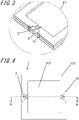
- Fig. 3 is an enlarged view of an area PI on the semiconductor device mounting board according to the embodiment of the present invention shown in Fig. 2A .
- Fig. 4 is a plan view of the semiconductor device mounting board 1 according to the embodiment of the present invention.
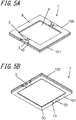
- Fig. 5A is a top perspective view of the semiconductor device mounting board 1 according to another embodiment of the present invention
- Fig. 5B is a bottom perspective view of the semiconductor device mounting board 1.
- FIG. 6A is a cross-sectional view of the semiconductor device mounting board 1 according to an embodiment of the present invention taken along line A-Ain Fig. 4
- Fig. 6B is a cross-sectional view of the semiconductor device mounting board 1 according to another embodiment of the present invention taken along line A-A in Fig. 4
- the semiconductor package 20 and the semiconductor device mounting board 1 include a first substrate 101, a second substrate 102, signal lines 2, grooves 3, feedthrough conductors 4, and side conductors 5.
- the semiconductor device mounting board 1 may further include a third substrate 103 as shown in Fig. 7A to Fig. 9D .
- Fig. 7A is a top perspective view of the semiconductor device mounting board 1 according to another embodiment of the present invention
- Fig. 7B is a bottom perspective view of the semiconductor device mounting board 1.
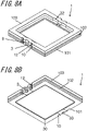
- Fig. 8A is a top perspective view of the semiconductor device mounting board 1 according to another embodiment of the present invention
- Fig. 8B is a bottom perspective view of the semiconductor device mounting board 1.
- Figs. 9A to 9D are exploded perspective views of a semiconductor device mounting board according to another embodiment of the present invention showing its conductors, and Fig. 9A shows a metal layer 35 on the upper surface of the third substrate 103, Fig.
- FIG. 9B shows signal lines 2 and a second ground conductor layer 8 on the upper surface of a second substrate 102
- Fig. 9C shows a first ground conductor layer 7, feedthrough conductors 4, and electrodes 6 on the upper surface of the first substrate 101
- Fig. 9D shows a metal layer 34 and side conductors 5 on the lower surface of the first substrate 101
- Fig. 10 is an enlarged view of an area P2 of the first ground conductor layer 7, the feedthrough conductor 4, and the electrode 6 on the upper surface of the first substrate shown in Fig. 9C .
- the semiconductor device mounting board 1 includes the first substrate 101 and a second substrate 102.
- the first substrate 101 has a mount area a on its upper surface, on which a semiconductor device 11 is mountable, and a peripheral area b, which surrounds the mount area a.
- the first substrate 101 is formed from ceramics such as sintered alumina (Al 2 O 3 ) or alumina ceramics.
- the second substrate 102 is located in the peripheral area b of the first substrate 101.
- the outer edge of the second substrate 102 is aligned with the outer edge of the first substrate 101.
- the second substrate 102 has a frame shape surrounding the mount area a.
- the second substrate 102 is formed from ceramics such as sintered alumina (Al 2 O 3 ) or alumina ceramics.
- the second substrate 102 has signal lines 2 on its upper surface. Each signal line 2 extends from one end on the inner edge of the second substrate 102 toward the other end on the outer edge of the second substrate 102.
- the signal lines 2 are formed from, for example, iron, copper, nickel, gold, chromium, cobalt, molybdenum, manganese, tungsten, or an alloy of any of these materials.
- the signal lines 2 are connected to the semiconductor device 11.
- the first substrate 101 has grooves 3 on the side surfaces, and side conductors 5 in the grooves 3.
- the grooves 3 extend from the lower surface to the upper surface of the first substrate 101.
- the side conductors 5 are located on the inner surfaces of the grooves 3 and connected to the signal lines 2, and the electrodes 6 and the feedthrough conductors 4 (described later).
- the grooves 3 are located inward from the outer edge of the second substrate 102.
- the side conductors 5 are formed from, for example, iron, copper, nickel, gold, chromium, cobalt, molybdenum, manganese, tungsten, or an alloy of any of these materials.
- the feedthrough conductors 4 are also electrically connected to the side conductors 5 through the electrodes 6 around the upper ends of the grooves 3 on the upper surface of the first substrate 101.
- the feedthrough conductors 4 are located at positions overlapping the other end of the corresponding signal line 2 and electrically connected to the end. This structure can more reliably transmit high-frequency electric signals from the feedthrough conductors 4 to the signal lines 2, and reduce transmission loss or reflection loss of the transmitted high-frequency electric signals.
- the grooves 3 are inward from the outer edge of the second substrate 102. In other words, the second substrate 102 is partially exposed along the grooves 3.
- the side conductors 5 in the grooves 3 thus reliably retain electrical conduction. In other words, this structure lowers the likelihood that the side conductors 5 are damaged or short-circuited due to external factors.
- the outer edge of the second substrate 102 may be located outward from the outer edge of the first substrate 101.
- the second substrate 102 has portions above the grooves 3 extending more outward from the grooves 3.
- the side conductors 5 in the grooves 3 are less susceptible to external factors, and reliably retain electrical conduction. This structure further lowers the likelihood that the side conductors 5 are damaged or short-circuited due to external factors.
- the semiconductor device mounting board 1 also includes the electrodes 6 and the first ground conductor layer 7.
- the electrodes 6 are located on the upper surface of the first substrate 101 or the lower surface of the second substrate 102 between the first substrate 101 and the second substrate 102, and electrically connected to the side conductors 5.
- the first ground conductor layer 7 is spaced from the electrodes 6.
- the electrodes 6 serve as a signal conductor layer
- the first ground conductor layer 7 serves as a ground conductor layer.
- This structure of the semiconductor device mounting board 1 including the electrodes 6 surrounded by the first ground conductor layer 7 can reduce the characteristic impedance of the side conductors 5 and the electrodes 6.
- This structure also lowers the likelihood that an electric field generated in a signal transmission portion from each side conductor 5 to the corresponding feedthrough conductor 4 through the electrode 6 extends in an unintended area, and allows electric field coupling between the electrode 6 and the first ground conductor layer 7.
- This structure thus regulates the distribution of the electric field of the signal transmission portion.
- This structure can transmit high-frequency electric signals through electric field coupling between the electrodes 6 and the first ground conductor layer 7. This structure stabilizes the characteristic impedance of the signal transmission portion.
- the semiconductor device mounting board 1 has the signal transmission portions surrounded by the ground potential portions, and thus regulates the distribution of the electric fields of the signal transmission portions.
- the semiconductor device mounting board 1 thus reduces variations in the characteristic impedance of the signal transmission portions.
- the high-performance semiconductor device mounting board 1 and the semiconductor package 20 can improve frequency response.
- the side conductors 5 When the side conductors 5 are electrically connected to an external mounting board with an electrically conductive bond such as solder, the bond forms a meniscus at the lower ends of the inner surfaces of the grooves 3. In this structure, the side conductors 5 are stably electrically connected to the external mounting board. In other words, the semiconductor device mounting board 1 reduces variations in the characteristic impedance of the signal transmission portions, and improves the frequency response.
- the semiconductor device mounting board 1 may further include second ground conductor layers 8 on the upper surface of the second substrate 102 to surround the signal lines 2. This structure forms coplanar lines in which the signal transmission portions are between the ground potential portions on the upper surface of the second substrate 102. The semiconductor device mounting board 1 further improves frequency response in the signal transmission portions.
- the first ground conductor layer 7 between the first substrate 101 and the second substrate 102 and spaced from the electrodes 6 is located under the signal lines 2 and the second ground conductor layers 8. This structure forms grounded coplanar lines.
- the semiconductor device mounting board 1 thus further improves frequency response in the signal transmission portions.
- each electrode 6 is located on the upper surface of the first substrate 101 or the lower surface of the second substrate 102 around the upper end of the corresponding groove 3 (the end facing the second substrate 102) in the direction perpendicular to the direction in which the corresponding side conductor 5 extends.
- Each electrode 6 is electrically connected to the corresponding side conductor 5.
- the outer edge of each electrode 6 is located inward from the outer edge of the side conductor 5 toward the semiconductor device mounting board 1. In other words, each electrode 6 in a bottom view is not exposed on the lower surface of the second substrate 102.
- an electrically conductive bond such as solder, used for electrically connecting the semiconductor package 20 to a mounting board avoids spreading to the electrodes 6 through the side conductors 5.
- This structure can thus reduce stress resulting from the difference in thermal expansion coefficients between the second substrate 102 and the bond.
- This structure also reduces unstable variations in the characteristic impedance due to spreading of the bond.
- the electrode 6 includes a second connection terminal 28, which serves as an inner-layer connection terminal protruding in the direction away from the groove 3.
- the feedthrough conductor 4 is connected to the surface of the second connection terminal 28 facing the second substrate 102.
- the electrode 6 is thus electrically connected to the signal line 2 with the second connection terminal 28 and the feedthrough conductor 4.
- the semiconductor device mounting board 1 thus has a large capacitance between the electrode 6 and the second connection terminal 28, and the first ground conductor layer 7. This structure is less likely to reduce the characteristic impedance.
- the signal transmission portion including each electrode 6 and the second connection terminal 28 thus easily achieves intended characteristic impedance.
- the semiconductor device mounting board 1 can be downsized, and can further improve the frequency response in the signal transmission portion.
- the second connection terminal 28 extends linearly from the center of the outer edge of the electrode 6 away from the groove 3, and has the feedthrough conductor 4 connected to the surface facing the second substrate 102.
- the semiconductor device mounting board 1 can have the shorter signal transmission portion including the electrode 6 and the second connection terminal 28, and further improves frequency response.
- the semiconductor device mounting board 1 also includes side ground conductors 31, which extend from side surfaces of the first substrate 101 to side surfaces of the second substrate 102 on both sides of the grooves 3.
- each signal transmission portion is between the ground potential portions also on the side surface.
- This structure of the semiconductor device mounting board 1 reduces unintended and unstable distribution of the electric fields in the signal transmission portions, and reduces variations in the characteristic impedance. Thus, the semiconductor device mounting board 1 further improves frequency response.
- the side ground conductors 31 may continuously extend from a side surface of the first substrate 101 to a side surface of the second substrate 102 on both sides of the corresponding groove 3.
- the semiconductor device mounting board 1 stabilizes the potential of the side ground conductors 31.
- each side ground conductor 31 on a side surface of the first substrate 101 may be aligned with the corresponding side ground conductor 31 on a side surface of the second substrate 102.
- the semiconductor device mounting board 1 reduces unintended and unstable distribution of the electric fields in the signal transmission portions, and reduces variations in the characteristic impedance in a more reliable manner.
- each electrode 6 has a substantially semi-circular profile in a plan view.
- This structure facilitates formation of the electrode 6 in manufacturing processes of the semiconductor device mounting board 1, and reduces stress concentration along the profile of the electrode 6.
- the semiconductor device mounting board 1 further reduces distorted distribution of the electric field along the profile of the electrode 6.
- This structure of the semiconductor device mounting board 1 thus lowers the likelihood that the electrode 6 is separated under stress along the profile of the electrode 6, or the first substrate 101 or the second substrate 102 crack, and further improves frequency response in the signal transmission portions.
- Signal electrodes 33 on the lower surface each have a substantially semi-circular profile in a plan view. With the same advantageous effects as described above, this structure stabilizes electrical connection between the semiconductor device 11 and an external mounting board, and improves the frequency response.
- a connection member such as solder
- an inner peripheral wall of the second substrate 102 surrounding the mount area a may include inner surface grooves 32 on both sides of the signal line 2 in a plan view of the semiconductor device mounting board 1.
- An inner surface ground conductor serving as a ground potential is located on the inner surface of each inner surface groove 32.
- a semiconductor device mounting board 1 may have a gap 30 in the lower surface of the first substrate 101, which is lower than the first ground conductor layer 7 and includes the signal electrodes 33.
- the gap 30 surrounds the mount area a in a plan view.
- the temperature inside the semiconductor device mounting board 1 changes or varies with heat generated by the semiconductor device 11 in manufacturing the semiconductor device mounting board 1 or the semiconductor package 20, or in operating the semiconductor package 20. This temperature change can cause thermal expansion or contraction of the semiconductor device mounting board 1 or the semiconductor device 11, thus generating stress.
- the gap 30 may reduce the stress in the semiconductor device mounting board 1. This structure lowers the likelihood that the semiconductor device mounting board 1 breaks or cracks.
- This structure also reduces deformation or warpage of the mount area a caused by deformation or warpage of the substrate 2 and allows the semiconductor device 11 to be stably mounted in the mount area a. This lowers the likelihood that the semiconductor device 11 breaks under such deformation or warpage in the mount area a.
- the gap 30 lowers the likelihood that the capacitance increases between each signal transmission portion and the ground potential portion and the characteristic impedance decreases.
- the signal transmission portion thus easily achieves intended characteristic impedance.
- the semiconductor device mounting board 1 can be downsized, and can further improve the frequency response in the signal transmission portion.
- the mount area a of the semiconductor device mounting board 1 may be formed from a metal. More specifically, the mount area a may be formed from a metal such as iron, copper, nickel, chromium, cobalt, or tungsten, or an alloy of any of these metals.
- the mount area a is electrically connected to the first ground conductor layer 7 with an electrically conductive bond, such as solder or brazing material. This structure improves heat dissipation from the semiconductor device mounting board 1.
- the mount area a, the first ground conductor layer 7, a ground conductor 22, and the side ground conductors 31 are connected to a ground layer 25, which is arranged on an external mounting board as described later, through the mount area a to stabilize the ground potentials.
- This structure increases the area over which the mount area a, which serves as a ground potential of the semiconductor device mounting board 1, is joined with the ground conductor on the external mounting board. This structure further stabilize the ground potential of the semiconductor device mounting board 1 including the mount area a.
- the semiconductor device mounting board 1 can further improve frequency response in the signal transmission portions. With the advantageous effects described above, the semiconductor device mounting board 1 including the gap 30 in the first substrate 101 reduces breaks and cracks in the semiconductor device mounting board 1 and thus reduces breaks in the semiconductor device 11. The semiconductor device mounting board 1 can further improve frequency response in the signal transmission portions.
- the grooves 3 are, for example, semi-elliptic or circular.
- the groove 3 is curved.
- the temperature inside the semiconductor device mounting board 1 changes or varies with heat generated by the semiconductor device 11 in manufacturing the semiconductor device mounting board 1 or the semiconductor package 20, or in operating the semiconductor package 20. This temperature change may cause thermal expansion or contraction of the semiconductor device mounting board 1, thus generating stress.
- Each groove 3 with a curve is less likely to receive concentrated stress, and thus prevents the first substrate 101, the side conductor 5, the electrode 6, the signal electrode 33 on the bottom surface, and the side ground conductor 31 from breaking or cracking.
- each groove 3 has the same profile as the electrode 6. With the advantageous effect described above, the semiconductor device mounting board 1 reduces stress concentration on specific portions of the groove 3 and the electrode 6.
- the first substrate 101 and the second substrate 102 have recesses 10 on their side surfaces.
- the recesses 10 extend from the lower surface of the first substrate 101 to the upper surface of the second substrate 102 on both sides of each groove 3 at positions spaced from each groove 3.
- Each recess 10 may receive the side ground conductor 31 on its inner circumferential surface.
- This structure increases the area of the side ground conductor 31, which serves as a ground conductor, and thus further stabilizes the ground potential of the semiconductor device mounting board 1. This structure further reduces unintended and unstable distribution of the electric field around the side conductors 5, and reduces variations in the characteristic impedance in a more reliable manner.
- the semiconductor device mounting board 1 further includes a third substrate 103 on the upper surface of the second substrate 102.
- the third substrate 103 is formed from, for example, the same material as the first substrate 101 and the second substrate 102, and has the same profile in a plan view.
- the third substrate 103 has, on side surfaces, second recesses 12 and cutouts 9 at positions overlapping the grooves 3 in a plan view. The cutouts 9 receive no ground conductor on the inner surface, whereas the second recesses 12 continuously receive the side ground conductors 31 on the inner surfaces.
- the third substrate 103 with no ground conductor on the inner surfaces of the cutouts 9 has a smaller distance between the signal lines 2 and the ground conductors 22 as the size of the semiconductor device mounting board 1 is reduced.
- This structure including the cutouts 9 lowers the likelihood that the capacitance increases between each signal transmission portion and the ground potential portion and the characteristic impedance decreases.
- each cutout 9 has a larger profile than the groove 3.
- the semiconductor device mounting board 1 thus reduces stress concentration on the second substrate 102 between the grooves 3 and the cutouts 9.
- the second substrate 102 is thus prevented from cracking or breaking.
- the recesses 10 and the second recesses 12 may have the same profile in a plan view. This reduces stress concentration on the interface between the recesses 10 and the second recesses 12.
- This structure reduces unintended and unstable distribution of the electric field around each side conductor 5, which forms the signal transmission portion of the semiconductor device mounting board 1, and reduces variations in the characteristic impedance.
- the semiconductor device mounting board 1 further improves frequency
- the first substrate 101 may have the metal layer 34, which serves as a lower surface, on its lower surface
- the third substrate 103 may have the metal layer 35, which serves as an upper surface, on its upper surface.
- the metal layer 34 on the lower surface facilitates electrical connection to a mounting board.
- the semiconductor device mounting board 1 improves heat dissipation characteristics through the metal layer 34.
- the metal layer 35 on the upper surface which receives the electric field generated to transmit high-frequency electric signals to the signal lines 2 through electric field coupling, reduces unintended and unstable distribution of the electric field around the signal lines 2.
- the semiconductor device mounting board 1 thus further improves frequency response in the signal transmission portions.
- Thermal stress occurs with heat of the semiconductor device 11 generated in manufacturing the semiconductor device mounting board 1 or the semiconductor package 20, or in operating the semiconductor package 20.
- the grooves 3 and the recesses 10 having the same profile and the cutouts 9 and the second recesses 12 having the same profile reduce thermal stress concentrating on the joint interfaces between the grooves 3 and the recesses 10, and between the cutouts 9 and the second recesses 12, as described above.
- the third substrate 103 has the second recesses 12, which receive the side ground conductors 31 on the inner surface. This structure reduces unintended and unstable distribution of the electric field at the ends of the signal lines 2 adjacent to the grooves 3, and reduces variations in the characteristic impedance. Thus, the semiconductor device mounting board 1 further improves frequency response.
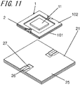
- Fig. 11 is an exploded perspective view of the semiconductor package 20 according to an embodiment of the present invention.
- the semiconductor device 11 is placed in the mount area a of the substrate 2, and is fixed to the substrate 2 by bonding with, for example, an adhesive.
- the semiconductor device 11 is then electrically connected to the signal lines 2 by, for example, wire bonding.
- the semiconductor device 11 is mounted on the semiconductor device mounting board 1 to complete the semiconductor package 20 as a product.
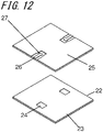
- Fig. 12 is an exploded perspective view of a mounting board 21 on which the semiconductor package 20 according to an embodiment of the present invention is mountable.
- Fig. 13A is a plan view of the semiconductor package 20 according to another embodiment of the present invention
- Fig. 13B is a plan view of the mounting board 21
- Fig. 13C is a plan view of a second layer of the mounting board
- Fig. 13D is a transparent plan view of the mounting board 21.
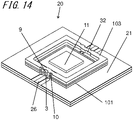
- Fig. 14 is an exploded perspective view of the semiconductor package 20 according to another embodiment of the present invention.
- the mounting board 21 includes, for example, multiple insulating layers.
- the mounting board 21 has signal conductors 26 and connection terminals 27, which are formed from a metal such as copper foil, on the upper surface of an upper one of the insulating layers.
- the signal conductors 26 and the connection terminals 27 are electrically connected to the side conductors 5 and the signal electrodes 33 on the lower surface with an electrically conductive bond, such as solder.
- High-frequency electric signals are transmitted through the signal conductors 26 and the connection terminals 27.
- the mounting board 21 also includes a ground layer 25 with a ground potential, which is formed from a metal such as copper foil.
- the ground layer 25 is located on the upper surface of the upper layer on both sides of the signal conductors 26 and surrounds the connection terminals 27 at a predetermined distance.
- the ground layer 25 is joined to, with a bond such as solder, the metal layer 34 on the lower surface of the semiconductor device mounting board 1, the side ground conductors 31, and the lower surface in the mount area a formed from a metal.
- the ground layer 25 is located without overlapping the electrodes 6 and the signal electrodes 33 on the lower surface.
- the ground layer 25 is located without overlapping the signal lines 2 in its signal transmission direction, that is, in the direction perpendicular to the direction from the signal lines 2 to the semiconductor device 11.
- the mounting board 21 includes an internal ground conductor 22.
- the ground conductor 22 includes an occupied area 23, in which the ground conductor 22 is located, and unoccupied areas 24, in which no ground conductor 22 is located.
- the unoccupied areas 24 of the ground conductor layer is located without overlapping at least the signal electrodes 33 on the lower surface and the connection terminals 27. This structure allows the characteristic impedance to be adjusted within an intended range when the semiconductor package 20 is mounted on the mounting board 21.
- An electrically conductive bond such as solder, that electrically connects the signal electrodes 33 on the lower surface to the connection terminals 27, and a meniscus formed from the bond on the side surfaces of the side conductors 5 otherwise increase the capacitance between the ground potential portion and each signal transmission portion between the signal conductor 26 and the side conductor 5, and reduce the characteristic impedance of the signal transmission portion.
- the unoccupied areas 24 may be located inward between a pair of side ground conductors 31 (around the side conductors 5) on both sides of each side conductor 5 in the signal transmission direction of the signal lines 2, that is, in the direction perpendicular to the direction from the signal lines 2 to the semiconductor device 11.
- This structure reduces unintended and unstable distribution of the electric field in each signal transmission portion between the signal conductor 26 and the side conductor 5, and reduces variations in the characteristic impedance.
- the semiconductor device mounting board 1 further improves the frequency response in the signal transmission portion.
Description
- The present invention relates to a semiconductor device mounting board on which a semiconductor device is mountable.
- As semiconductor devices tend toward high-frequency response, the demand is increasing for semiconductor device mounting boards and semiconductor packages with high-performance that can improve frequency response of semiconductor devices. To obtain such semiconductor packages, a semiconductor device is mounted on a mount area on a semiconductor device mounting board, and the electrodes of the semiconductor device are electrically connected to signal lines by, for example, wire bonding to complete the product (refer to, for example,
Japanese Unexamined Patent Application Publication No. 2012-156428 - However, with the technique described in
Japanese Unexamined Patent Application Publication No. 2012-156428 -
JP 2009 266905 A - The present invention provides a semiconductor device mounting board according to
claim 1, and a semiconductor package according toclaim 7. Further embodiments of the present invention are disclosed in the dependent claims. -
-
Fig. 1 is a perspective view of a semiconductor package according to an embodiment of the present invention. -
Fig. 2A is a top perspective view of a semiconductor device mounting board according to the embodiment of the present invention, andFig. 2B is a bottom perspective view of the semiconductor device mounting board. -
Fig. 3 is an enlarged view of an area PI on the semiconductor device mounting board according to the embodiment of the present invention shown inFig. 2A . -
Fig. 4 is a plan view of the semiconductor device mounting board according to the embodiment of the present invention. -
Figs 5A is a top perspective view of a semiconductor device mounting board according to another embodiment of the present invention, andFig. 5B is a bottom perspective view of the semiconductor device mounting board. -
Fig. 6A is a cross-sectional view of a semiconductor device mounting board according to an embodiment of the present invention taken along line A-A inFig. 4 , andFig. 6B is a cross-sectional view of a semiconductor device mounting board according to another embodiment of the present invention taken along line A-A inFig. 4 . -
Fig. 7A is a top perspective view of a semiconductor device mounting board according to another embodiment of the present invention, andFig. 7B is a bottom perspective view of the semiconductor device mounting board. -
Fig. 8A is a top perspective view of a semiconductor device mounting board according to another embodiment of the present invention, andFig. 8B is a bottom perspective view of the semiconductor device mounting board. -
Figs. 9A to 9D are exploded perspective views of a semiconductor device mounting board according to another embodiment of the present invention showing its conductors, andFig. 9A shows a metal layer on the upper surface of a third substrate,Fig. 9B shows signal lines and a ground conductor layer on the upper surface of a second substrate,Fig. 9C shows a first ground conductor layer and electrodes on the upper surface of a first substrate, andFig. 9D shows a metal layer on the lower surface of the first substrate. -
Fig. 10 is an enlarged view of an area P2 of the first ground conductor layer and the electrodes on the upper surface of the first substrate shown inFig. 9C . -
Fig. 11 is an exploded perspective view of a semiconductor package according to an embodiment of the present invention. -
Fig. 12 is an exploded perspective view of a mounting board on which a semiconductor package according to an embodiment of the present invention is mountable. -
Fig. 13A is a plan view of a semiconductor package according to another embodiment of the present invention,Fig. 13B is a plan view of a mounting board in the semiconductor package,Fig. 13C is a plan view of a second layer of the mounting board, andFig. 13D is a transparent plan view of the mounting board. -
Fig. 14 is an exploded perspective view of a semiconductor package according to another embodiment of the present invention. - A semiconductor
device mounting board 1 according to an embodiment of the present invention will now be described in detail with reference to the drawings. The same components are given the same reference numerals in the figures. -
Fig. 1 is a perspective view of asemiconductor package 20 according to an embodiment of the present invention.Fig. 2A is a top perspective view of the semiconductordevice mounting board 1 according to the embodiment of the present invention, andFig. 2B is a bottom perspective view of the semiconductordevice mounting board 1.Fig. 3 is an enlarged view of an area PI on the semiconductor device mounting board according to the embodiment of the present invention shown inFig. 2A .Fig. 4 is a plan view of the semiconductordevice mounting board 1 according to the embodiment of the present invention.Fig. 5A is a top perspective view of the semiconductordevice mounting board 1 according to another embodiment of the present invention, andFig. 5B is a bottom perspective view of the semiconductordevice mounting board 1.Fig. 6A is a cross-sectional view of the semiconductordevice mounting board 1 according to an embodiment of the present invention taken along line A-AinFig. 4 , andFig. 6B is a cross-sectional view of the semiconductordevice mounting board 1 according to another embodiment of the present invention taken along line A-A inFig. 4 . In these drawings, thesemiconductor package 20 and the semiconductordevice mounting board 1 include afirst substrate 101, asecond substrate 102,signal lines 2,grooves 3,feedthrough conductors 4, andside conductors 5. - The semiconductor
device mounting board 1 according to another embodiment of the present invention may further include athird substrate 103 as shown inFig. 7A to Fig. 9D .Fig. 7A is a top perspective view of the semiconductordevice mounting board 1 according to another embodiment of the present invention, andFig. 7B is a bottom perspective view of the semiconductordevice mounting board 1.Fig. 8A is a top perspective view of the semiconductordevice mounting board 1 according to another embodiment of the present invention, andFig. 8B is a bottom perspective view of the semiconductordevice mounting board 1.Figs. 9A to 9D are exploded perspective views of a semiconductor device mounting board according to another embodiment of the present invention showing its conductors, andFig. 9A shows ametal layer 35 on the upper surface of thethird substrate 103,Fig. 9B showssignal lines 2 and a secondground conductor layer 8 on the upper surface of asecond substrate 102,Fig. 9C shows a firstground conductor layer 7,feedthrough conductors 4, andelectrodes 6 on the upper surface of thefirst substrate 101, andFig. 9D shows ametal layer 34 andside conductors 5 on the lower surface of thefirst substrate 101.Fig. 10 is an enlarged view of an area P2 of the firstground conductor layer 7, thefeedthrough conductor 4, and theelectrode 6 on the upper surface of the first substrate shown inFig. 9C . - The semiconductor
device mounting board 1 includes thefirst substrate 101 and asecond substrate 102. Thefirst substrate 101 has a mount area a on its upper surface, on which asemiconductor device 11 is mountable, and a peripheral area b, which surrounds the mount area a. Thefirst substrate 101 is formed from ceramics such as sintered alumina (Al2O3) or alumina ceramics. - The
second substrate 102 is located in the peripheral area b of thefirst substrate 101. In a plan view of the semiconductordevice mounting board 1, the outer edge of thesecond substrate 102 is aligned with the outer edge of thefirst substrate 101. Thesecond substrate 102 has a frame shape surrounding the mount area a. In the same manner as thefirst substrate 101, thesecond substrate 102 is formed from ceramics such as sintered alumina (Al2O3) or alumina ceramics. - The
second substrate 102 hassignal lines 2 on its upper surface. Eachsignal line 2 extends from one end on the inner edge of thesecond substrate 102 toward the other end on the outer edge of thesecond substrate 102. Thesignal lines 2 are formed from, for example, iron, copper, nickel, gold, chromium, cobalt, molybdenum, manganese, tungsten, or an alloy of any of these materials. Thesignal lines 2 are connected to thesemiconductor device 11. - The
first substrate 101 hasgrooves 3 on the side surfaces, andside conductors 5 in thegrooves 3. Thegrooves 3 extend from the lower surface to the upper surface of thefirst substrate 101. Theside conductors 5 are located on the inner surfaces of thegrooves 3 and connected to thesignal lines 2, and theelectrodes 6 and the feedthrough conductors 4 (described later). In a plan view of the semiconductordevice mounting board 1, thegrooves 3 are located inward from the outer edge of thesecond substrate 102. Theside conductors 5 are formed from, for example, iron, copper, nickel, gold, chromium, cobalt, molybdenum, manganese, tungsten, or an alloy of any of these materials. - The
feedthrough conductors 4, which are electrically connected to thesignal lines 2, extend through thesecond substrate 102 from the upper to lower surfaces of the substrate. Thefeedthrough conductors 4 are also electrically connected to theside conductors 5 through theelectrodes 6 around the upper ends of thegrooves 3 on the upper surface of thefirst substrate 101. Thefeedthrough conductors 4 are located at positions overlapping the other end of thecorresponding signal line 2 and electrically connected to the end. This structure can more reliably transmit high-frequency electric signals from thefeedthrough conductors 4 to thesignal lines 2, and reduce transmission loss or reflection loss of the transmitted high-frequency electric signals. - In a plan view, the
grooves 3 are inward from the outer edge of thesecond substrate 102. In other words, thesecond substrate 102 is partially exposed along thegrooves 3. Theside conductors 5 in thegrooves 3 thus reliably retain electrical conduction. In other words, this structure lowers the likelihood that theside conductors 5 are damaged or short-circuited due to external factors. - In a plan view, the outer edge of the
second substrate 102 may be located outward from the outer edge of thefirst substrate 101. In this structure, thesecond substrate 102 has portions above thegrooves 3 extending more outward from thegrooves 3. In other words, theside conductors 5 in thegrooves 3 are less susceptible to external factors, and reliably retain electrical conduction. This structure further lowers the likelihood that theside conductors 5 are damaged or short-circuited due to external factors. - As shown in
Figs. 6A, 6B , and10 , the semiconductordevice mounting board 1 also includes theelectrodes 6 and the firstground conductor layer 7. Theelectrodes 6 are located on the upper surface of thefirst substrate 101 or the lower surface of thesecond substrate 102 between thefirst substrate 101 and thesecond substrate 102, and electrically connected to theside conductors 5. The firstground conductor layer 7 is spaced from theelectrodes 6. In the semiconductordevice mounting board 1, theelectrodes 6 serve as a signal conductor layer, and the firstground conductor layer 7 serves as a ground conductor layer. This structure of the semiconductordevice mounting board 1 including theelectrodes 6 surrounded by the firstground conductor layer 7 can reduce the characteristic impedance of theside conductors 5 and theelectrodes 6. This structure also lowers the likelihood that an electric field generated in a signal transmission portion from eachside conductor 5 to the correspondingfeedthrough conductor 4 through theelectrode 6 extends in an unintended area, and allows electric field coupling between theelectrode 6 and the firstground conductor layer 7. This structure thus regulates the distribution of the electric field of the signal transmission portion. This structure can transmit high-frequency electric signals through electric field coupling between theelectrodes 6 and the firstground conductor layer 7. This structure stabilizes the characteristic impedance of the signal transmission portion. - More specifically, the semiconductor
device mounting board 1 has the signal transmission portions surrounded by the ground potential portions, and thus regulates the distribution of the electric fields of the signal transmission portions. The semiconductordevice mounting board 1 thus reduces variations in the characteristic impedance of the signal transmission portions. Thus, the high-performance semiconductordevice mounting board 1 and thesemiconductor package 20 can improve frequency response. - When the
side conductors 5 are electrically connected to an external mounting board with an electrically conductive bond such as solder, the bond forms a meniscus at the lower ends of the inner surfaces of thegrooves 3. In this structure, theside conductors 5 are stably electrically connected to the external mounting board. In other words, the semiconductordevice mounting board 1 reduces variations in the characteristic impedance of the signal transmission portions, and improves the frequency response. - The semiconductor
device mounting board 1 may further include second ground conductor layers 8 on the upper surface of thesecond substrate 102 to surround the signal lines 2. This structure forms coplanar lines in which the signal transmission portions are between the ground potential portions on the upper surface of thesecond substrate 102. The semiconductordevice mounting board 1 further improves frequency response in the signal transmission portions. The firstground conductor layer 7 between thefirst substrate 101 and thesecond substrate 102 and spaced from theelectrodes 6 is located under thesignal lines 2 and the second ground conductor layers 8. This structure forms grounded coplanar lines. The semiconductordevice mounting board 1 thus further improves frequency response in the signal transmission portions. - As shown in
Figs. 6A, 6B , and10 , eachelectrode 6 is located on the upper surface of thefirst substrate 101 or the lower surface of thesecond substrate 102 around the upper end of the corresponding groove 3 (the end facing the second substrate 102) in the direction perpendicular to the direction in which thecorresponding side conductor 5 extends. Eachelectrode 6 is electrically connected to thecorresponding side conductor 5. In a bottom view, the outer edge of eachelectrode 6 is located inward from the outer edge of theside conductor 5 toward the semiconductordevice mounting board 1. In other words, eachelectrode 6 in a bottom view is not exposed on the lower surface of thesecond substrate 102. In the structure including theelectrodes 6 not exposed on the lower surface of thesecond substrate 102, an electrically conductive bond, such as solder, used for electrically connecting thesemiconductor package 20 to a mounting board avoids spreading to theelectrodes 6 through theside conductors 5. This structure can thus reduce stress resulting from the difference in thermal expansion coefficients between thesecond substrate 102 and the bond. This structure also reduces unstable variations in the characteristic impedance due to spreading of the bond. Theside conductors 5 and theelectrodes 6, which serve as the signal transmission portions, thus more reliably retain frequency response. - As shown in
Fig. 10 , theelectrode 6 includes asecond connection terminal 28, which serves as an inner-layer connection terminal protruding in the direction away from thegroove 3. Thefeedthrough conductor 4 is connected to the surface of thesecond connection terminal 28 facing thesecond substrate 102. Theelectrode 6 is thus electrically connected to thesignal line 2 with thesecond connection terminal 28 and thefeedthrough conductor 4. The semiconductordevice mounting board 1 thus has a large capacitance between theelectrode 6 and thesecond connection terminal 28, and the firstground conductor layer 7. This structure is less likely to reduce the characteristic impedance. The signal transmission portion including eachelectrode 6 and thesecond connection terminal 28 thus easily achieves intended characteristic impedance. The semiconductordevice mounting board 1 can be downsized, and can further improve the frequency response in the signal transmission portion. - In a plan view, the
second connection terminal 28 extends linearly from the center of the outer edge of theelectrode 6 away from thegroove 3, and has thefeedthrough conductor 4 connected to the surface facing thesecond substrate 102. The semiconductordevice mounting board 1 can have the shorter signal transmission portion including theelectrode 6 and thesecond connection terminal 28, and further improves frequency response. - The semiconductor
device mounting board 1 also includesside ground conductors 31, which extend from side surfaces of thefirst substrate 101 to side surfaces of thesecond substrate 102 on both sides of thegrooves 3. In this structure, each signal transmission portion is between the ground potential portions also on the side surface. This structure of the semiconductordevice mounting board 1 reduces unintended and unstable distribution of the electric fields in the signal transmission portions, and reduces variations in the characteristic impedance. Thus, the semiconductordevice mounting board 1 further improves frequency response. Theside ground conductors 31 may continuously extend from a side surface of thefirst substrate 101 to a side surface of thesecond substrate 102 on both sides of thecorresponding groove 3. Thus, the semiconductordevice mounting board 1 stabilizes the potential of theside ground conductors 31. In a plan view, eachside ground conductor 31 on a side surface of thefirst substrate 101 may be aligned with the correspondingside ground conductor 31 on a side surface of thesecond substrate 102. The semiconductordevice mounting board 1 reduces unintended and unstable distribution of the electric fields in the signal transmission portions, and reduces variations in the characteristic impedance in a more reliable manner. - As shown in
Fig. 10 , eachelectrode 6 has a substantially semi-circular profile in a plan view. This structure facilitates formation of theelectrode 6 in manufacturing processes of the semiconductordevice mounting board 1, and reduces stress concentration along the profile of theelectrode 6. The semiconductordevice mounting board 1 further reduces distorted distribution of the electric field along the profile of theelectrode 6. This structure of the semiconductordevice mounting board 1 thus lowers the likelihood that theelectrode 6 is separated under stress along the profile of theelectrode 6, or thefirst substrate 101 or thesecond substrate 102 crack, and further improves frequency response in the signal transmission portions.Signal electrodes 33 on the lower surface each have a substantially semi-circular profile in a plan view. With the same advantageous effects as described above, this structure stabilizes electrical connection between thesemiconductor device 11 and an external mounting board, and improves the frequency response. When thesemiconductor package 20 is mounted on an external mounting board with thesignal electrodes 33 on the lower surface using a connection member such as solder, less stress concentrates around thesignal electrodes 33 on the lower surface and the connection member. - In some embodiments, an inner peripheral wall of the
second substrate 102 surrounding the mount area a may includeinner surface grooves 32 on both sides of thesignal line 2 in a plan view of the semiconductordevice mounting board 1. An inner surface ground conductor serving as a ground potential is located on the inner surface of eachinner surface groove 32. The semiconductordevice mounting board 1 with this structure reduces unintended and unstable distribution of the electric field at the end of thesignal lines 2 adjacent to the mount area a, and reduces variations in the characteristic impedance. The semiconductordevice mounting board 1 thus further improves frequency response. - As shown in
Figs. 5B ,6B , and8B , a semiconductordevice mounting board 1 according to another embodiment of the present invention may have agap 30 in the lower surface of thefirst substrate 101, which is lower than the firstground conductor layer 7 and includes thesignal electrodes 33. Thegap 30 surrounds the mount area a in a plan view. The temperature inside the semiconductordevice mounting board 1 changes or varies with heat generated by thesemiconductor device 11 in manufacturing the semiconductordevice mounting board 1 or thesemiconductor package 20, or in operating thesemiconductor package 20. This temperature change can cause thermal expansion or contraction of the semiconductordevice mounting board 1 or thesemiconductor device 11, thus generating stress. Thegap 30 may reduce the stress in the semiconductordevice mounting board 1. This structure lowers the likelihood that the semiconductordevice mounting board 1 breaks or cracks. This structure also reduces deformation or warpage of the mount area a caused by deformation or warpage of thesubstrate 2 and allows thesemiconductor device 11 to be stably mounted in the mount area a. This lowers the likelihood that thesemiconductor device 11 breaks under such deformation or warpage in the mount area a. - In a small-sized semiconductor
device mounting board 1 with a shorter distance between the firstground conductor layer 7 and theside conductors 5, thesignal electrodes 33 on the bottom surface, and theelectrodes 6, thegap 30 lowers the likelihood that the capacitance increases between each signal transmission portion and the ground potential portion and the characteristic impedance decreases. The signal transmission portion thus easily achieves intended characteristic impedance. The semiconductordevice mounting board 1 can be downsized, and can further improve the frequency response in the signal transmission portion. - The mount area a of the semiconductor
device mounting board 1 may be formed from a metal. More specifically, the mount area a may be formed from a metal such as iron, copper, nickel, chromium, cobalt, or tungsten, or an alloy of any of these metals. The mount area a is electrically connected to the firstground conductor layer 7 with an electrically conductive bond, such as solder or brazing material. This structure improves heat dissipation from the semiconductordevice mounting board 1. The mount area a, the firstground conductor layer 7, aground conductor 22, and theside ground conductors 31 are connected to aground layer 25, which is arranged on an external mounting board as described later, through the mount area a to stabilize the ground potentials. This structure increases the area over which the mount area a, which serves as a ground potential of the semiconductordevice mounting board 1, is joined with the ground conductor on the external mounting board. This structure further stabilize the ground potential of the semiconductordevice mounting board 1 including the mount area a. - The semiconductor
device mounting board 1 can further improve frequency response in the signal transmission portions. With the advantageous effects described above, the semiconductordevice mounting board 1 including thegap 30 in thefirst substrate 101 reduces breaks and cracks in the semiconductordevice mounting board 1 and thus reduces breaks in thesemiconductor device 11. The semiconductordevice mounting board 1 can further improve frequency response in the signal transmission portions. - In a plan view, the
grooves 3 are, for example, semi-elliptic or circular. Thegroove 3 is curved. The temperature inside the semiconductordevice mounting board 1 changes or varies with heat generated by thesemiconductor device 11 in manufacturing the semiconductordevice mounting board 1 or thesemiconductor package 20, or in operating thesemiconductor package 20. This temperature change may cause thermal expansion or contraction of the semiconductordevice mounting board 1, thus generating stress. Eachgroove 3 with a curve is less likely to receive concentrated stress, and thus prevents thefirst substrate 101, theside conductor 5, theelectrode 6, thesignal electrode 33 on the bottom surface, and theside ground conductor 31 from breaking or cracking. In a plan view, eachgroove 3 has the same profile as theelectrode 6. With the advantageous effect described above, the semiconductordevice mounting board 1 reduces stress concentration on specific portions of thegroove 3 and theelectrode 6. - As shown in
Fig. 3 , in a side view, thefirst substrate 101 and thesecond substrate 102 haverecesses 10 on their side surfaces. Therecesses 10 extend from the lower surface of thefirst substrate 101 to the upper surface of thesecond substrate 102 on both sides of eachgroove 3 at positions spaced from eachgroove 3. Eachrecess 10 may receive theside ground conductor 31 on its inner circumferential surface. This structure increases the area of theside ground conductor 31, which serves as a ground conductor, and thus further stabilizes the ground potential of the semiconductordevice mounting board 1. This structure further reduces unintended and unstable distribution of the electric field around theside conductors 5, and reduces variations in the characteristic impedance in a more reliable manner. - As shown in
Figs. 7Ato 9D , the semiconductordevice mounting board 1 further includes athird substrate 103 on the upper surface of thesecond substrate 102. Thethird substrate 103 is formed from, for example, the same material as thefirst substrate 101 and thesecond substrate 102, and has the same profile in a plan view. For example, thethird substrate 103 has, on side surfaces, second recesses 12 andcutouts 9 at positions overlapping thegrooves 3 in a plan view. Thecutouts 9 receive no ground conductor on the inner surface, whereas thesecond recesses 12 continuously receive theside ground conductors 31 on the inner surfaces. Thethird substrate 103 with no ground conductor on the inner surfaces of thecutouts 9 has a smaller distance between thesignal lines 2 and theground conductors 22 as the size of the semiconductordevice mounting board 1 is reduced. This structure including thecutouts 9 lowers the likelihood that the capacitance increases between each signal transmission portion and the ground potential portion and the characteristic impedance decreases. In a plan view, eachcutout 9 has a larger profile than thegroove 3. The semiconductordevice mounting board 1 thus reduces stress concentration on thesecond substrate 102 between thegrooves 3 and thecutouts 9. Thesecond substrate 102 is thus prevented from cracking or breaking. Therecesses 10 and thesecond recesses 12 may have the same profile in a plan view. This reduces stress concentration on the interface between therecesses 10 and the second recesses 12. This structure reduces unintended and unstable distribution of the electric field around eachside conductor 5, which forms the signal transmission portion of the semiconductordevice mounting board 1, and reduces variations in the characteristic impedance. Thus, the semiconductordevice mounting board 1 further improves frequency response in the signal transmission portions. - As shown in
Figs. 9A to 9D , thefirst substrate 101 may have themetal layer 34, which serves as a lower surface, on its lower surface, and thethird substrate 103 may have themetal layer 35, which serves as an upper surface, on its upper surface. Themetal layer 34 on the lower surface facilitates electrical connection to a mounting board. The semiconductordevice mounting board 1 improves heat dissipation characteristics through themetal layer 34. Themetal layer 35 on the upper surface, which receives the electric field generated to transmit high-frequency electric signals to thesignal lines 2 through electric field coupling, reduces unintended and unstable distribution of the electric field around the signal lines 2. The semiconductordevice mounting board 1 thus further improves frequency response in the signal transmission portions. - Thermal stress occurs with heat of the
semiconductor device 11 generated in manufacturing the semiconductordevice mounting board 1 or thesemiconductor package 20, or in operating thesemiconductor package 20. Thegrooves 3 and therecesses 10 having the same profile and thecutouts 9 and thesecond recesses 12 having the same profile reduce thermal stress concentrating on the joint interfaces between thegrooves 3 and therecesses 10, and between thecutouts 9 and the second recesses 12, as described above. Thethird substrate 103 has the second recesses 12, which receive theside ground conductors 31 on the inner surface. This structure reduces unintended and unstable distribution of the electric field at the ends of thesignal lines 2 adjacent to thegrooves 3, and reduces variations in the characteristic impedance. Thus, the semiconductordevice mounting board 1 further improves frequency response. -
Fig. 11 is an exploded perspective view of thesemiconductor package 20 according to an embodiment of the present invention. To assemble thesemiconductor package 20, thesemiconductor device 11 is placed in the mount area a of thesubstrate 2, and is fixed to thesubstrate 2 by bonding with, for example, an adhesive. Thesemiconductor device 11 is then electrically connected to thesignal lines 2 by, for example, wire bonding. Thesemiconductor device 11 is mounted on the semiconductordevice mounting board 1 to complete thesemiconductor package 20 as a product. - Another embodiment of the
semiconductor package 20 will now be described with reference toFigs. 12 to 14 .Fig. 12 is an exploded perspective view of a mountingboard 21 on which thesemiconductor package 20 according to an embodiment of the present invention is mountable.Fig. 13A is a plan view of thesemiconductor package 20 according to another embodiment of the present invention,Fig. 13B is a plan view of the mountingboard 21,Fig. 13C is a plan view of a second layer of the mounting board, andFig. 13D is a transparent plan view of the mountingboard 21.Fig. 14 is an exploded perspective view of thesemiconductor package 20 according to another embodiment of the present invention. - The mounting
board 21 includes, for example, multiple insulating layers. The mountingboard 21 hassignal conductors 26 andconnection terminals 27, which are formed from a metal such as copper foil, on the upper surface of an upper one of the insulating layers. Thesignal conductors 26 and theconnection terminals 27 are electrically connected to theside conductors 5 and thesignal electrodes 33 on the lower surface with an electrically conductive bond, such as solder. High-frequency electric signals are transmitted through thesignal conductors 26 and theconnection terminals 27. The mountingboard 21 also includes aground layer 25 with a ground potential, which is formed from a metal such as copper foil. Theground layer 25 is located on the upper surface of the upper layer on both sides of thesignal conductors 26 and surrounds theconnection terminals 27 at a predetermined distance. - The
ground layer 25 is joined to, with a bond such as solder, themetal layer 34 on the lower surface of the semiconductordevice mounting board 1, theside ground conductors 31, and the lower surface in the mount area a formed from a metal. The mountingboard 21, which includes theconnection terminals 27, thesignal conductors 26, and theground layer 25 on the upper surface, forms coplanar lines, which are planar transmission lines. In a plan view, theground layer 25 is located without overlapping theelectrodes 6 and thesignal electrodes 33 on the lower surface. Theground layer 25 is located without overlapping thesignal lines 2 in its signal transmission direction, that is, in the direction perpendicular to the direction from thesignal lines 2 to thesemiconductor device 11. - The mounting
board 21 includes aninternal ground conductor 22. Theground conductor 22 includes an occupiedarea 23, in which theground conductor 22 is located, andunoccupied areas 24, in which noground conductor 22 is located. In a plan view, theunoccupied areas 24 of the ground conductor layer is located without overlapping at least thesignal electrodes 33 on the lower surface and theconnection terminals 27. This structure allows the characteristic impedance to be adjusted within an intended range when thesemiconductor package 20 is mounted on the mountingboard 21. An electrically conductive bond, such as solder, that electrically connects thesignal electrodes 33 on the lower surface to theconnection terminals 27, and a meniscus formed from the bond on the side surfaces of theside conductors 5 otherwise increase the capacitance between the ground potential portion and each signal transmission portion between thesignal conductor 26 and theside conductor 5, and reduce the characteristic impedance of the signal transmission portion. - In a plan view, the
unoccupied areas 24 may be located inward between a pair of side ground conductors 31 (around the side conductors 5) on both sides of eachside conductor 5 in the signal transmission direction of thesignal lines 2, that is, in the direction perpendicular to the direction from thesignal lines 2 to thesemiconductor device 11. This structure reduces unintended and unstable distribution of the electric field in each signal transmission portion between thesignal conductor 26 and theside conductor 5, and reduces variations in the characteristic impedance. Thus, the semiconductordevice mounting board 1 further improves the frequency response in the signal transmission portion. - The present invention is not limited to the embodiments described above, and may be modified in various manners without departing from the scope of the present invention.
-
- 1
- semiconductor device mounting board
- 101
- first substrate
- 102
- second substrate
- 103
- third substrate
- a
- mount area
- b
- peripheral area
- 2
- signal line
- 3
- groove
- 4
- feedthrough conductor
- 5
- side conductor
- 6
- electrode
- 7
- first ground conductor layer
- 8
- second ground conductor layer
- 9
- cutout
- 10
- recess
- 11
- semiconductor device
- 12
- second recess
- 20
- semiconductor package
- 21
- mounting board
- 22
- ground conductor
- 23
- occupied area
- 24
- unoccupied area
- 25
- ground layer
- 26
- signal conductor
- 27
- connection terminal
- 28
- second connection terminal
- 30
- gap
- 31
- side ground conductor
- 32
- inner surface groove
- 33
- signal electrode on lower surface
- 34
- metal layer on lower surface
- 35
- metal layer on upper surface
Claims (8)
- A semiconductor device mounting board (1), comprising:a first substrate (101) including an upper surface having a mount area (a) on which a semiconductor device (11) is mountable and a peripheral area (b) surrounding the mount area (a);a second substrate (102) having a frame shape surrounding the mount area (a), the second substrate (102) located in the peripheral area (b) of the first substrate (101) to align with an outer edge of the first substrate (101);a signal line (2) on an upper surface of the second substrate (102) and extending from an inner edge toward an outer edge of the second substrate (102);a groove (3) on a side surface of the first substrate (101) and extending from a lower surface to the upper surface of the first substrate (101);a feedthrough conductor (4) inside the second substrate (102) and connected to the signal line (2);a side conductor (5) on an inner surface of the groove (3) in the first substrate (101) and electrically connectable to the feedthrough conductor (4); and characterized in that the semiconductor device mounting board (1) further comprisesrecesses (10) on side surfaces of the first substrate (101) and the second substrate (102), the recesses (10) being on both sides of the groove (3) at positions spaced from the groove (3) in a side view,wherein the groove (3) is inward from the outer edge of the second substrate (102).
- The semiconductor device mounting board (1) according to claim 1, further comprising:an electrode (6) on a lower surface of the second substrate (102), the electrode (6) connecting the side conductor (5) to the feedthrough conductor (4),wherein an outer edge of the electrode (6) is inward from an outer edge of the side conductor (5) in a bottom view.
- The semiconductor device mounting board (1) according to claim 2, further comprising:a first ground conductor layer (7) between the first substrate (101) and the second substrate (102), the first ground conductor layer (7) being spaced from the electrode (6), anda ground conductor layer (8) on the upper surface of the second substrate (102), the ground conductor layer (8) being on both sides and spaced from the signal line (2).
- The semiconductor device mounting board (1) according to any one of claims 1 to 3, wherein
the outer edge of the second substrate (102) is outward from the outer edge of the first substrate (101) in a plan view. - The semiconductor device mounting board (1) according to any one of claims 1 to 4, further comprising:
a third substrate (103) having a frame shape surrounding the mount area (a) on the upper surface of the second substrate (102). - The semiconductor device mounting board (1) according to claim 5, wherein
the third substrate (103) has a cutout (9) in a side surface of the third substrate (103) at a position overlapping the groove (3) in a side view. - A semiconductor package (20), comprising:the semiconductor device mounting board (1) according to any one of claims 1 to 6; anda semiconductor device (11) mountable in the mount area (a) and electrically connected to the signal line (2).
- The semiconductor package (20) according to claim 7, further comprising:a mounting board (21) joined to a lower surface of the first substrate (101),wherein the mounting board (21) includes an area (23) occupied by a ground conductor (22) and an area (24) unoccupied by the ground conductor (22) inside the mounting board (21), and the area (24) unoccupied by the ground conductor (22) is located to overlap the side conductor (5).
Applications Claiming Priority (2)
| Application Number | Priority Date | Filing Date | Title |
|---|---|---|---|
| JP2016148006 | 2016-07-28 | ||
| PCT/JP2017/026604 WO2018021209A1 (en) | 2016-07-28 | 2017-07-24 | Substrate for mounting semiconductor element and semiconductor device |
Publications (3)
| Publication Number | Publication Date |
|---|---|
| EP3493252A1 EP3493252A1 (en) | 2019-06-05 |
| EP3493252A4 EP3493252A4 (en) | 2020-04-15 |
| EP3493252B1 true EP3493252B1 (en) | 2022-10-26 |
Family
ID=61017333
Family Applications (1)
| Application Number | Title | Priority Date | Filing Date |
|---|---|---|---|
| EP17834215.0A Active EP3493252B1 (en) | 2016-07-28 | 2017-07-24 | Substrate for mounting semiconductor element and semiconductor device |
Country Status (5)
| Country | Link |
|---|---|
| US (1) | US10777493B2 (en) |
| EP (1) | EP3493252B1 (en) |
| JP (2) | JP6853252B2 (en) |
| CN (1) | CN109478537B (en) |
| WO (1) | WO2018021209A1 (en) |
Families Citing this family (5)
| Publication number | Priority date | Publication date | Assignee | Title |
|---|---|---|---|---|
| KR102107025B1 (en) * | 2018-09-14 | 2020-05-07 | 삼성전기주식회사 | Electronic component module and manufacturing method thereof |
| JP7237609B2 (en) * | 2019-01-28 | 2023-03-13 | 京セラ株式会社 | Packages for electronic components and electronic devices |
| JP7286389B2 (en) * | 2019-04-15 | 2023-06-05 | キヤノン株式会社 | Wireless communication device, wireless communication system and communication method |
| TWI771610B (en) * | 2019-09-02 | 2022-07-21 | 矽品精密工業股份有限公司 | Electronic package, carrier structure and manufacturing method thereof |
| WO2023054419A1 (en) | 2021-09-30 | 2023-04-06 | 京セラ株式会社 | Substrate for mounting semiconductor element and semiconductor device |
Family Cites Families (24)
| Publication number | Priority date | Publication date | Assignee | Title |
|---|---|---|---|---|
| JPH01253260A (en) * | 1988-03-31 | 1989-10-09 | Nec Corp | Semiconductor device |
| JPH05218653A (en) * | 1992-01-31 | 1993-08-27 | Sumitomo Metal Ind Ltd | Ceramic multilayer circuit board |
| JP3296160B2 (en) * | 1995-10-24 | 2002-06-24 | 富士通株式会社 | Display unit |
| JP3457802B2 (en) | 1996-04-26 | 2003-10-20 | 京セラ株式会社 | High frequency semiconductor device |
| JPH09232351A (en) * | 1996-02-23 | 1997-09-05 | Fujitsu Ltd | Package for electronic element |
| JP4131524B2 (en) * | 1997-09-18 | 2008-08-13 | シチズン電子株式会社 | Surface mount photocoupler |
| JP3570887B2 (en) | 1998-04-28 | 2004-09-29 | 京セラ株式会社 | High frequency wiring board |
| JP3178452B2 (en) * | 1999-02-24 | 2001-06-18 | 日本電気株式会社 | Package for semiconductor device and its mounting structure |
| JP2001223286A (en) | 2000-02-10 | 2001-08-17 | New Japan Radio Co Ltd | Board for leadless chip carrier and leadless chip carrier |
| JP2002190540A (en) * | 2000-12-20 | 2002-07-05 | Kyocera Corp | Storage package for semiconductor element |
| JP2003068921A (en) * | 2001-08-22 | 2003-03-07 | Toyo Commun Equip Co Ltd | Surface mount electronic component |
| JP2003218265A (en) * | 2002-01-21 | 2003-07-31 | Tokyo Denpa Co Ltd | Electronic component container |
| JP3911473B2 (en) * | 2002-11-26 | 2007-05-09 | 京セラ株式会社 | Semiconductor device mounting substrate |
| JP2004200243A (en) * | 2002-12-16 | 2004-07-15 | Kyocera Corp | Package for housing semiconductor element and semiconductor device |
| JP4199019B2 (en) * | 2003-02-17 | 2008-12-17 | アルプス電気株式会社 | Surface mount circuit module |
| JP4447553B2 (en) * | 2003-07-03 | 2010-04-07 | 株式会社ルネサステクノロジ | Multifunction card device |
| JP2005129818A (en) * | 2003-10-27 | 2005-05-19 | Kyocera Corp | Wiring board, and mounting structure thereof |
| JP4511336B2 (en) * | 2004-12-24 | 2010-07-28 | 京セラ株式会社 | Multi-cavity wiring board and method for manufacturing electronic device |
| US8354688B2 (en) * | 2008-03-25 | 2013-01-15 | Bridge Semiconductor Corporation | Semiconductor chip assembly with bump/base/ledge heat spreader, dual adhesives and cavity in bump |
| JP2009266905A (en) * | 2008-04-23 | 2009-11-12 | Panasonic Corp | Semiconductor device |
| US20100270668A1 (en) * | 2009-04-28 | 2010-10-28 | Wafer-Level Packaging Portfolio Llc | Dual Interconnection in Stacked Memory and Controller Module |
| JP5791283B2 (en) | 2011-01-28 | 2015-10-07 | 京セラ株式会社 | Electronic component storage package and electronic device including the same |
| WO2012165434A1 (en) | 2011-05-31 | 2012-12-06 | 京セラ株式会社 | Element housing package, component for semiconductor device, and semiconductor device |
| CN104103747A (en) * | 2013-04-03 | 2014-10-15 | 光宝电子(广州)有限公司 | Packaging structure for light emitting diode |
-
2017
- 2017-07-24 CN CN201780045405.9A patent/CN109478537B/en active Active
- 2017-07-24 WO PCT/JP2017/026604 patent/WO2018021209A1/en unknown
- 2017-07-24 EP EP17834215.0A patent/EP3493252B1/en active Active
- 2017-07-24 JP JP2018529863A patent/JP6853252B2/en active Active
- 2017-07-24 US US16/320,049 patent/US10777493B2/en active Active
-
2021
- 2021-03-10 JP JP2021038490A patent/JP7049500B2/en active Active
Also Published As
| Publication number | Publication date |
|---|---|
| JPWO2018021209A1 (en) | 2019-05-09 |
| CN109478537A (en) | 2019-03-15 |
| JP6853252B2 (en) | 2021-03-31 |
| JP7049500B2 (en) | 2022-04-06 |
| WO2018021209A1 (en) | 2018-02-01 |
| EP3493252A4 (en) | 2020-04-15 |
| CN109478537B (en) | 2022-08-19 |
| US10777493B2 (en) | 2020-09-15 |
| JP2021101475A (en) | 2021-07-08 |
| EP3493252A1 (en) | 2019-06-05 |
| US20190221507A1 (en) | 2019-07-18 |
Similar Documents
| Publication | Publication Date | Title |
|---|---|---|
| EP3493252B1 (en) | Substrate for mounting semiconductor element and semiconductor device | |
| EP2738798B1 (en) | Package for accommodating semiconductor element, semiconductor device provided with same, and electronic device | |
| CN107534023B (en) | Semiconductor element package, semiconductor device, and mounting structure | |
| JP6243510B2 (en) | Electronic component storage package and electronic device | |
| EP3118895B1 (en) | Package for housing an electronic component and electronic device including the package | |
| JP6633656B2 (en) | Wiring board, optical semiconductor element package and optical semiconductor device | |
| JP6151794B2 (en) | Circuit board, electronic component storage package, and electronic device | |
| JP6971921B2 (en) | Differential transmission lines, wiring boards and semiconductor packages | |
| JP4903738B2 (en) | Electronic component storage package and electronic device | |
| JP6856468B2 (en) | Wiring boards, electronic component packages and electronic devices | |
| TW200417140A (en) | Dielectric component array | |
| JP3935082B2 (en) | High frequency package | |
| JP6940286B2 (en) | Wiring boards, electronic component packages and electronic devices | |
| JP6673764B2 (en) | Semiconductor element mounting substrate and semiconductor device | |
| JP2017098070A (en) | Electronic device | |
| JP6591912B2 (en) | Semiconductor device package and semiconductor device | |
| WO2022230848A1 (en) | Electronic component mounting package and electronic device | |
| JP3600729B2 (en) | High frequency circuit package | |
| JP2019129209A (en) | Wiring board, package for electronic component, and electronic device | |
| JPH11339898A (en) | High frequency input and output terminal, and package for high frequency circuit | |
| JP2014127589A (en) | Package for housing element and mounting structure | |
| JP2020017622A (en) | Wiring board, package for electronic component, and electronic device | |
| JP2004253714A (en) | Wiring board with lead frame |
Legal Events
| Date | Code | Title | Description |
|---|---|---|---|
| STAA | Information on the status of an ep patent application or granted ep patent |
Free format text: STATUS: THE INTERNATIONAL PUBLICATION HAS BEEN MADE |
|
| PUAI | Public reference made under article 153(3) epc to a published international application that has entered the european phase |
Free format text: ORIGINAL CODE: 0009012 |
|
| STAA | Information on the status of an ep patent application or granted ep patent |
Free format text: STATUS: REQUEST FOR EXAMINATION WAS MADE |
|
| 17P | Request for examination filed |
Effective date: 20190218 |
|
| AK | Designated contracting states |
Kind code of ref document: A1 Designated state(s): AL AT BE BG CH CY CZ DE DK EE ES FI FR GB GR HR HU IE IS IT LI LT LU LV MC MK MT NL NO PL PT RO RS SE SI SK SM TR |
|
| AX | Request for extension of the european patent |
Extension state: BA ME |
|
| DAV | Request for validation of the european patent (deleted) | ||
| DAX | Request for extension of the european patent (deleted) | ||
| A4 | Supplementary search report drawn up and despatched |
Effective date: 20200316 |
|
| RIC1 | Information provided on ipc code assigned before grant |
Ipc: H05K 1/14 20060101ALI20200310BHEP Ipc: H01L 23/12 20060101AFI20200310BHEP Ipc: H05K 3/46 20060101ALI20200310BHEP Ipc: H05K 1/02 20060101ALI20200310BHEP Ipc: H05K 3/34 20060101ALI20200310BHEP Ipc: H05K 3/40 20060101ALI20200310BHEP |
|
| GRAP | Despatch of communication of intention to grant a patent |
Free format text: ORIGINAL CODE: EPIDOSNIGR1 |
|
| STAA | Information on the status of an ep patent application or granted ep patent |
Free format text: STATUS: GRANT OF PATENT IS INTENDED |
|
| INTG | Intention to grant announced |
Effective date: 20220520 |
|
| GRAS | Grant fee paid |
Free format text: ORIGINAL CODE: EPIDOSNIGR3 |
|
| GRAA | (expected) grant |
Free format text: ORIGINAL CODE: 0009210 |
|
| STAA | Information on the status of an ep patent application or granted ep patent |
Free format text: STATUS: THE PATENT HAS BEEN GRANTED |
|
| AK | Designated contracting states |
Kind code of ref document: B1 Designated state(s): AL AT BE BG CH CY CZ DE DK EE ES FI FR GB GR HR HU IE IS IT LI LT LU LV MC MK MT NL NO PL PT RO RS SE SI SK SM TR |
|
| REG | Reference to a national code |
Ref country code: GB Ref legal event code: FG4D |
|
| REG | Reference to a national code |
Ref country code: CH Ref legal event code: EP |
|
| REG | Reference to a national code |
Ref country code: DE Ref legal event code: R096 Ref document number: 602017063096 Country of ref document: DE |
|
| REG | Reference to a national code |
Ref country code: AT Ref legal event code: REF Ref document number: 1527679 Country of ref document: AT Kind code of ref document: T Effective date: 20221115 |
|
| REG | Reference to a national code |
Ref country code: IE Ref legal event code: FG4D |
|
| REG | Reference to a national code |
Ref country code: LT Ref legal event code: MG9D |
|
| REG | Reference to a national code |
Ref country code: NL Ref legal event code: MP Effective date: 20221026 |
|
| REG | Reference to a national code |
Ref country code: AT Ref legal event code: MK05 Ref document number: 1527679 Country of ref document: AT Kind code of ref document: T Effective date: 20221026 |
|
| PG25 | Lapsed in a contracting state [announced via postgrant information from national office to epo] |
Ref country code: NL Free format text: LAPSE BECAUSE OF FAILURE TO SUBMIT A TRANSLATION OF THE DESCRIPTION OR TO PAY THE FEE WITHIN THE PRESCRIBED TIME-LIMIT Effective date: 20221026 |
|
| PG25 | Lapsed in a contracting state [announced via postgrant information from national office to epo] |
Ref country code: SE Free format text: LAPSE BECAUSE OF FAILURE TO SUBMIT A TRANSLATION OF THE DESCRIPTION OR TO PAY THE FEE WITHIN THE PRESCRIBED TIME-LIMIT Effective date: 20221026 Ref country code: PT Free format text: LAPSE BECAUSE OF FAILURE TO SUBMIT A TRANSLATION OF THE DESCRIPTION OR TO PAY THE FEE WITHIN THE PRESCRIBED TIME-LIMIT Effective date: 20230227 Ref country code: NO Free format text: LAPSE BECAUSE OF FAILURE TO SUBMIT A TRANSLATION OF THE DESCRIPTION OR TO PAY THE FEE WITHIN THE PRESCRIBED TIME-LIMIT Effective date: 20230126 Ref country code: LT Free format text: LAPSE BECAUSE OF FAILURE TO SUBMIT A TRANSLATION OF THE DESCRIPTION OR TO PAY THE FEE WITHIN THE PRESCRIBED TIME-LIMIT Effective date: 20221026 Ref country code: FI Free format text: LAPSE BECAUSE OF FAILURE TO SUBMIT A TRANSLATION OF THE DESCRIPTION OR TO PAY THE FEE WITHIN THE PRESCRIBED TIME-LIMIT Effective date: 20221026 Ref country code: ES Free format text: LAPSE BECAUSE OF FAILURE TO SUBMIT A TRANSLATION OF THE DESCRIPTION OR TO PAY THE FEE WITHIN THE PRESCRIBED TIME-LIMIT Effective date: 20221026 Ref country code: AT Free format text: LAPSE BECAUSE OF FAILURE TO SUBMIT A TRANSLATION OF THE DESCRIPTION OR TO PAY THE FEE WITHIN THE PRESCRIBED TIME-LIMIT Effective date: 20221026 |
|
| PG25 | Lapsed in a contracting state [announced via postgrant information from national office to epo] |
Ref country code: RS Free format text: LAPSE BECAUSE OF FAILURE TO SUBMIT A TRANSLATION OF THE DESCRIPTION OR TO PAY THE FEE WITHIN THE PRESCRIBED TIME-LIMIT Effective date: 20221026 Ref country code: PL Free format text: LAPSE BECAUSE OF FAILURE TO SUBMIT A TRANSLATION OF THE DESCRIPTION OR TO PAY THE FEE WITHIN THE PRESCRIBED TIME-LIMIT Effective date: 20221026 Ref country code: LV Free format text: LAPSE BECAUSE OF FAILURE TO SUBMIT A TRANSLATION OF THE DESCRIPTION OR TO PAY THE FEE WITHIN THE PRESCRIBED TIME-LIMIT Effective date: 20221026 Ref country code: IS Free format text: LAPSE BECAUSE OF FAILURE TO SUBMIT A TRANSLATION OF THE DESCRIPTION OR TO PAY THE FEE WITHIN THE PRESCRIBED TIME-LIMIT Effective date: 20230226 Ref country code: HR Free format text: LAPSE BECAUSE OF FAILURE TO SUBMIT A TRANSLATION OF THE DESCRIPTION OR TO PAY THE FEE WITHIN THE PRESCRIBED TIME-LIMIT Effective date: 20221026 Ref country code: GR Free format text: LAPSE BECAUSE OF FAILURE TO SUBMIT A TRANSLATION OF THE DESCRIPTION OR TO PAY THE FEE WITHIN THE PRESCRIBED TIME-LIMIT Effective date: 20230127 |
|
| P01 | Opt-out of the competence of the unified patent court (upc) registered |
Effective date: 20230505 |
|
| REG | Reference to a national code |
Ref country code: DE Ref legal event code: R097 Ref document number: 602017063096 Country of ref document: DE |
|
| PG25 | Lapsed in a contracting state [announced via postgrant information from national office to epo] |
Ref country code: SM Free format text: LAPSE BECAUSE OF FAILURE TO SUBMIT A TRANSLATION OF THE DESCRIPTION OR TO PAY THE FEE WITHIN THE PRESCRIBED TIME-LIMIT Effective date: 20221026 Ref country code: RO Free format text: LAPSE BECAUSE OF FAILURE TO SUBMIT A TRANSLATION OF THE DESCRIPTION OR TO PAY THE FEE WITHIN THE PRESCRIBED TIME-LIMIT Effective date: 20221026 Ref country code: EE Free format text: LAPSE BECAUSE OF FAILURE TO SUBMIT A TRANSLATION OF THE DESCRIPTION OR TO PAY THE FEE WITHIN THE PRESCRIBED TIME-LIMIT Effective date: 20221026 Ref country code: DK Free format text: LAPSE BECAUSE OF FAILURE TO SUBMIT A TRANSLATION OF THE DESCRIPTION OR TO PAY THE FEE WITHIN THE PRESCRIBED TIME-LIMIT Effective date: 20221026 Ref country code: CZ Free format text: LAPSE BECAUSE OF FAILURE TO SUBMIT A TRANSLATION OF THE DESCRIPTION OR TO PAY THE FEE WITHIN THE PRESCRIBED TIME-LIMIT Effective date: 20221026 |
|
| PGFP | Annual fee paid to national office [announced via postgrant information from national office to epo] |
Ref country code: FR Payment date: 20230608 Year of fee payment: 7 |
|
| PG25 | Lapsed in a contracting state [announced via postgrant information from national office to epo] |
Ref country code: SK Free format text: LAPSE BECAUSE OF FAILURE TO SUBMIT A TRANSLATION OF THE DESCRIPTION OR TO PAY THE FEE WITHIN THE PRESCRIBED TIME-LIMIT Effective date: 20221026 Ref country code: AL Free format text: LAPSE BECAUSE OF FAILURE TO SUBMIT A TRANSLATION OF THE DESCRIPTION OR TO PAY THE FEE WITHIN THE PRESCRIBED TIME-LIMIT Effective date: 20221026 |
|
| PLBE | No opposition filed within time limit |
Free format text: ORIGINAL CODE: 0009261 |
|
| STAA | Information on the status of an ep patent application or granted ep patent |
Free format text: STATUS: NO OPPOSITION FILED WITHIN TIME LIMIT |
|
| 26N | No opposition filed |
Effective date: 20230727 |
|
| PGFP | Annual fee paid to national office [announced via postgrant information from national office to epo] |
Ref country code: GB Payment date: 20230601 Year of fee payment: 7 |
|
| PG25 | Lapsed in a contracting state [announced via postgrant information from national office to epo] |
Ref country code: SI Free format text: LAPSE BECAUSE OF FAILURE TO SUBMIT A TRANSLATION OF THE DESCRIPTION OR TO PAY THE FEE WITHIN THE PRESCRIBED TIME-LIMIT Effective date: 20221026 |
|
| PGFP | Annual fee paid to national office [announced via postgrant information from national office to epo] |
Ref country code: DE Payment date: 20230531 Year of fee payment: 7 |
|
| PG25 | Lapsed in a contracting state [announced via postgrant information from national office to epo] |
Ref country code: MC Free format text: LAPSE BECAUSE OF FAILURE TO SUBMIT A TRANSLATION OF THE DESCRIPTION OR TO PAY THE FEE WITHIN THE PRESCRIBED TIME-LIMIT Effective date: 20221026 |
|
| PG25 | Lapsed in a contracting state [announced via postgrant information from national office to epo] |
Ref country code: MC Free format text: LAPSE BECAUSE OF FAILURE TO SUBMIT A TRANSLATION OF THE DESCRIPTION OR TO PAY THE FEE WITHIN THE PRESCRIBED TIME-LIMIT Effective date: 20221026 |
|
| REG | Reference to a national code |
Ref country code: CH Ref legal event code: PL |
|
| PG25 | Lapsed in a contracting state [announced via postgrant information from national office to epo] |
Ref country code: LU Free format text: LAPSE BECAUSE OF NON-PAYMENT OF DUE FEES Effective date: 20230724 |
|
| PG25 | Lapsed in a contracting state [announced via postgrant information from national office to epo] |
Ref country code: LU Free format text: LAPSE BECAUSE OF NON-PAYMENT OF DUE FEES Effective date: 20230724 |