EP3454372A1 - Lichtemittierende diode - Google Patents
Lichtemittierende diode Download PDFInfo
- Publication number
- EP3454372A1 EP3454372A1 EP17792825.6A EP17792825A EP3454372A1 EP 3454372 A1 EP3454372 A1 EP 3454372A1 EP 17792825 A EP17792825 A EP 17792825A EP 3454372 A1 EP3454372 A1 EP 3454372A1
- Authority
- EP
- European Patent Office
- Prior art keywords
- light emitting
- layer
- type semiconductor
- contact
- emitting diode
- Prior art date
- Legal status (The legal status is an assumption and is not a legal conclusion. Google has not performed a legal analysis and makes no representation as to the accuracy of the status listed.)
- Granted
Links
- 239000004065 semiconductor Substances 0.000 claims abstract description 359
- 238000009413 insulation Methods 0.000 claims description 218
- 239000000758 substrate Substances 0.000 claims description 140
- 238000002955 isolation Methods 0.000 claims description 91
- 125000006850 spacer group Chemical group 0.000 claims description 64
- 238000000034 method Methods 0.000 claims description 54
- 230000008569 process Effects 0.000 claims description 31
- 229920005989 resin Polymers 0.000 claims description 31
- 239000011347 resin Substances 0.000 claims description 31
- 229910052751 metal Inorganic materials 0.000 claims description 24
- 239000002184 metal Substances 0.000 claims description 24
- 239000000463 material Substances 0.000 claims description 23
- 238000006243 chemical reaction Methods 0.000 claims description 19
- 239000000853 adhesive Substances 0.000 claims description 14
- 230000001070 adhesive effect Effects 0.000 claims description 14
- 239000010410 layer Substances 0.000 description 900
- VYPSYNLAJGMNEJ-UHFFFAOYSA-N Silicium dioxide Chemical compound O=[Si]=O VYPSYNLAJGMNEJ-UHFFFAOYSA-N 0.000 description 33
- 229920002120 photoresistant polymer Polymers 0.000 description 25
- 239000010936 titanium Substances 0.000 description 17
- 229910052759 nickel Inorganic materials 0.000 description 15
- JMASRVWKEDWRBT-UHFFFAOYSA-N Gallium nitride Chemical compound [Ga]#N JMASRVWKEDWRBT-UHFFFAOYSA-N 0.000 description 14
- 229910052681 coesite Inorganic materials 0.000 description 14
- 229910052906 cristobalite Inorganic materials 0.000 description 14
- 239000000377 silicon dioxide Substances 0.000 description 14
- 239000002356 single layer Substances 0.000 description 14
- 229910052682 stishovite Inorganic materials 0.000 description 14
- 229910052905 tridymite Inorganic materials 0.000 description 14
- 229910002601 GaN Inorganic materials 0.000 description 13
- 238000005530 etching Methods 0.000 description 12
- 238000004519 manufacturing process Methods 0.000 description 11
- 230000003287 optical effect Effects 0.000 description 11
- 229910052804 chromium Inorganic materials 0.000 description 10
- 238000000605 extraction Methods 0.000 description 9
- 230000017525 heat dissipation Effects 0.000 description 9
- GWEVSGVZZGPLCZ-UHFFFAOYSA-N Titan oxide Chemical compound O=[Ti]=O GWEVSGVZZGPLCZ-UHFFFAOYSA-N 0.000 description 8
- 150000004767 nitrides Chemical class 0.000 description 8
- 238000000206 photolithography Methods 0.000 description 8
- 230000007480 spreading Effects 0.000 description 8
- 238000003892 spreading Methods 0.000 description 8
- 238000005229 chemical vapour deposition Methods 0.000 description 7
- 229910052802 copper Inorganic materials 0.000 description 7
- 229910000679 solder Inorganic materials 0.000 description 7
- 229910052581 Si3N4 Inorganic materials 0.000 description 6
- 238000005336 cracking Methods 0.000 description 6
- 229910052737 gold Inorganic materials 0.000 description 6
- 229910052763 palladium Inorganic materials 0.000 description 6
- 229910052697 platinum Inorganic materials 0.000 description 6
- 229910052594 sapphire Inorganic materials 0.000 description 6
- 239000010980 sapphire Substances 0.000 description 6
- 239000012535 impurity Substances 0.000 description 5
- 238000012858 packaging process Methods 0.000 description 5
- 238000000059 patterning Methods 0.000 description 5
- 238000002310 reflectometry Methods 0.000 description 5
- 229910052814 silicon oxide Inorganic materials 0.000 description 5
- 230000008901 benefit Effects 0.000 description 4
- 230000015572 biosynthetic process Effects 0.000 description 4
- 238000005566 electron beam evaporation Methods 0.000 description 4
- 230000006870 function Effects 0.000 description 4
- 239000004973 liquid crystal related substance Substances 0.000 description 4
- 238000000465 moulding Methods 0.000 description 4
- 229920006128 poly(nonamethylene terephthalamide) Polymers 0.000 description 4
- 229910052709 silver Inorganic materials 0.000 description 4
- 229910052719 titanium Inorganic materials 0.000 description 4
- 239000012790 adhesive layer Substances 0.000 description 3
- AMGQUBHHOARCQH-UHFFFAOYSA-N indium;oxotin Chemical compound [In].[Sn]=O AMGQUBHHOARCQH-UHFFFAOYSA-N 0.000 description 3
- 239000007769 metal material Substances 0.000 description 3
- 239000000203 mixture Substances 0.000 description 3
- 150000003071 polychlorinated biphenyls Chemical class 0.000 description 3
- 239000011241 protective layer Substances 0.000 description 3
- HQVNEWCFYHHQES-UHFFFAOYSA-N silicon nitride Chemical compound N12[Si]34N5[Si]62N3[Si]51N64 HQVNEWCFYHHQES-UHFFFAOYSA-N 0.000 description 3
- 229910001316 Ag alloy Inorganic materials 0.000 description 2
- 229910000838 Al alloy Inorganic materials 0.000 description 2
- 229910002704 AlGaN Inorganic materials 0.000 description 2
- 229910052782 aluminium Inorganic materials 0.000 description 2
- 239000003963 antioxidant agent Substances 0.000 description 2
- 230000003078 antioxidant effect Effects 0.000 description 2
- 239000002019 doping agent Substances 0.000 description 2
- 230000000694 effects Effects 0.000 description 2
- 238000009713 electroplating Methods 0.000 description 2
- 238000001704 evaporation Methods 0.000 description 2
- 230000008020 evaporation Effects 0.000 description 2
- 229910052738 indium Inorganic materials 0.000 description 2
- 239000011810 insulating material Substances 0.000 description 2
- ZKATWMILCYLAPD-UHFFFAOYSA-N niobium pentoxide Chemical compound O=[Nb](=O)O[Nb](=O)=O ZKATWMILCYLAPD-UHFFFAOYSA-N 0.000 description 2
- 238000003825 pressing Methods 0.000 description 2
- 230000009467 reduction Effects 0.000 description 2
- 229910052703 rhodium Inorganic materials 0.000 description 2
- 229910052710 silicon Inorganic materials 0.000 description 2
- 238000004544 sputter deposition Methods 0.000 description 2
- 239000010409 thin film Substances 0.000 description 2
- OGIDPMRJRNCKJF-UHFFFAOYSA-N titanium oxide Inorganic materials [Ti]=O OGIDPMRJRNCKJF-UHFFFAOYSA-N 0.000 description 2
- PIGFYZPCRLYGLF-UHFFFAOYSA-N Aluminum nitride Chemical compound [Al]#N PIGFYZPCRLYGLF-UHFFFAOYSA-N 0.000 description 1
- CIWBSHSKHKDKBQ-JLAZNSOCSA-N Ascorbic acid Chemical compound OC[C@H](O)[C@H]1OC(=O)C(O)=C1O CIWBSHSKHKDKBQ-JLAZNSOCSA-N 0.000 description 1
- 229910004205 SiNX Inorganic materials 0.000 description 1
- XUIMIQQOPSSXEZ-UHFFFAOYSA-N Silicon Chemical compound [Si] XUIMIQQOPSSXEZ-UHFFFAOYSA-N 0.000 description 1
- 229910008599 TiW Inorganic materials 0.000 description 1
- 230000003064 anti-oxidating effect Effects 0.000 description 1
- 230000004888 barrier function Effects 0.000 description 1
- 230000033228 biological regulation Effects 0.000 description 1
- 230000008859 change Effects 0.000 description 1
- 239000011248 coating agent Substances 0.000 description 1
- 238000000576 coating method Methods 0.000 description 1
- 238000004891 communication Methods 0.000 description 1
- 150000001875 compounds Chemical class 0.000 description 1
- 230000007547 defect Effects 0.000 description 1
- 238000000151 deposition Methods 0.000 description 1
- 238000011161 development Methods 0.000 description 1
- 238000007772 electroless plating Methods 0.000 description 1
- 230000005496 eutectics Effects 0.000 description 1
- 239000010408 film Substances 0.000 description 1
- 229910052733 gallium Inorganic materials 0.000 description 1
- 229910052732 germanium Inorganic materials 0.000 description 1
- 238000000227 grinding Methods 0.000 description 1
- APFVFJFRJDLVQX-UHFFFAOYSA-N indium atom Chemical compound [In] APFVFJFRJDLVQX-UHFFFAOYSA-N 0.000 description 1
- 238000003780 insertion Methods 0.000 description 1
- 230000037431 insertion Effects 0.000 description 1
- 238000009434 installation Methods 0.000 description 1
- 239000012774 insulation material Substances 0.000 description 1
- 238000010030 laminating Methods 0.000 description 1
- 229910001635 magnesium fluoride Inorganic materials 0.000 description 1
- 230000004048 modification Effects 0.000 description 1
- 238000012986 modification Methods 0.000 description 1
- 230000003647 oxidation Effects 0.000 description 1
- 238000007254 oxidation reaction Methods 0.000 description 1
- 239000004033 plastic Substances 0.000 description 1
- 229920001296 polysiloxane Polymers 0.000 description 1
- 230000004044 response Effects 0.000 description 1
- 239000010703 silicon Substances 0.000 description 1
- 235000012239 silicon dioxide Nutrition 0.000 description 1
- 238000004528 spin coating Methods 0.000 description 1
- 239000000126 substance Substances 0.000 description 1
- KKEYFWRCBNTPAC-UHFFFAOYSA-L terephthalate(2-) Chemical compound [O-]C(=O)C1=CC=C(C([O-])=O)C=C1 KKEYFWRCBNTPAC-UHFFFAOYSA-L 0.000 description 1
- 229910052718 tin Inorganic materials 0.000 description 1
- 230000007704 transition Effects 0.000 description 1
- 229910052721 tungsten Inorganic materials 0.000 description 1
- 238000001039 wet etching Methods 0.000 description 1
Images


Classifications
-
- H—ELECTRICITY
- H01—ELECTRIC ELEMENTS
- H01L—SEMICONDUCTOR DEVICES NOT COVERED BY CLASS H10
- H01L33/00—Semiconductor devices with at least one potential-jump barrier or surface barrier specially adapted for light emission; Processes or apparatus specially adapted for the manufacture or treatment thereof or of parts thereof; Details thereof
- H01L33/48—Semiconductor devices with at least one potential-jump barrier or surface barrier specially adapted for light emission; Processes or apparatus specially adapted for the manufacture or treatment thereof or of parts thereof; Details thereof characterised by the semiconductor body packages
- H01L33/62—Arrangements for conducting electric current to or from the semiconductor body, e.g. lead-frames, wire-bonds or solder balls
-
- H—ELECTRICITY
- H01—ELECTRIC ELEMENTS
- H01L—SEMICONDUCTOR DEVICES NOT COVERED BY CLASS H10
- H01L25/00—Assemblies consisting of a plurality of individual semiconductor or other solid state devices ; Multistep manufacturing processes thereof
- H01L25/03—Assemblies consisting of a plurality of individual semiconductor or other solid state devices ; Multistep manufacturing processes thereof all the devices being of a type provided for in the same subgroup of groups H01L27/00 - H01L33/00, or in a single subclass of H10K, H10N, e.g. assemblies of rectifier diodes
- H01L25/04—Assemblies consisting of a plurality of individual semiconductor or other solid state devices ; Multistep manufacturing processes thereof all the devices being of a type provided for in the same subgroup of groups H01L27/00 - H01L33/00, or in a single subclass of H10K, H10N, e.g. assemblies of rectifier diodes the devices not having separate containers
- H01L25/075—Assemblies consisting of a plurality of individual semiconductor or other solid state devices ; Multistep manufacturing processes thereof all the devices being of a type provided for in the same subgroup of groups H01L27/00 - H01L33/00, or in a single subclass of H10K, H10N, e.g. assemblies of rectifier diodes the devices not having separate containers the devices being of a type provided for in group H01L33/00
- H01L25/0753—Assemblies consisting of a plurality of individual semiconductor or other solid state devices ; Multistep manufacturing processes thereof all the devices being of a type provided for in the same subgroup of groups H01L27/00 - H01L33/00, or in a single subclass of H10K, H10N, e.g. assemblies of rectifier diodes the devices not having separate containers the devices being of a type provided for in group H01L33/00 the devices being arranged next to each other
-
- H—ELECTRICITY
- H01—ELECTRIC ELEMENTS
- H01L—SEMICONDUCTOR DEVICES NOT COVERED BY CLASS H10
- H01L27/00—Devices consisting of a plurality of semiconductor or other solid-state components formed in or on a common substrate
- H01L27/15—Devices consisting of a plurality of semiconductor or other solid-state components formed in or on a common substrate including semiconductor components with at least one potential-jump barrier or surface barrier specially adapted for light emission
- H01L27/153—Devices consisting of a plurality of semiconductor or other solid-state components formed in or on a common substrate including semiconductor components with at least one potential-jump barrier or surface barrier specially adapted for light emission in a repetitive configuration, e.g. LED bars
-
- H—ELECTRICITY
- H01—ELECTRIC ELEMENTS
- H01L—SEMICONDUCTOR DEVICES NOT COVERED BY CLASS H10
- H01L33/00—Semiconductor devices with at least one potential-jump barrier or surface barrier specially adapted for light emission; Processes or apparatus specially adapted for the manufacture or treatment thereof or of parts thereof; Details thereof
- H01L33/02—Semiconductor devices with at least one potential-jump barrier or surface barrier specially adapted for light emission; Processes or apparatus specially adapted for the manufacture or treatment thereof or of parts thereof; Details thereof characterised by the semiconductor bodies
- H01L33/10—Semiconductor devices with at least one potential-jump barrier or surface barrier specially adapted for light emission; Processes or apparatus specially adapted for the manufacture or treatment thereof or of parts thereof; Details thereof characterised by the semiconductor bodies with a light reflecting structure, e.g. semiconductor Bragg reflector
-
- H—ELECTRICITY
- H01—ELECTRIC ELEMENTS
- H01L—SEMICONDUCTOR DEVICES NOT COVERED BY CLASS H10
- H01L33/00—Semiconductor devices with at least one potential-jump barrier or surface barrier specially adapted for light emission; Processes or apparatus specially adapted for the manufacture or treatment thereof or of parts thereof; Details thereof
- H01L33/02—Semiconductor devices with at least one potential-jump barrier or surface barrier specially adapted for light emission; Processes or apparatus specially adapted for the manufacture or treatment thereof or of parts thereof; Details thereof characterised by the semiconductor bodies
- H01L33/26—Materials of the light emitting region
- H01L33/30—Materials of the light emitting region containing only elements of group III and group V of the periodic system
- H01L33/32—Materials of the light emitting region containing only elements of group III and group V of the periodic system containing nitrogen
- H01L33/325—Materials of the light emitting region containing only elements of group III and group V of the periodic system containing nitrogen characterised by the doping materials
-
- H—ELECTRICITY
- H01—ELECTRIC ELEMENTS
- H01L—SEMICONDUCTOR DEVICES NOT COVERED BY CLASS H10
- H01L33/00—Semiconductor devices with at least one potential-jump barrier or surface barrier specially adapted for light emission; Processes or apparatus specially adapted for the manufacture or treatment thereof or of parts thereof; Details thereof
- H01L33/36—Semiconductor devices with at least one potential-jump barrier or surface barrier specially adapted for light emission; Processes or apparatus specially adapted for the manufacture or treatment thereof or of parts thereof; Details thereof characterised by the electrodes
- H01L33/38—Semiconductor devices with at least one potential-jump barrier or surface barrier specially adapted for light emission; Processes or apparatus specially adapted for the manufacture or treatment thereof or of parts thereof; Details thereof characterised by the electrodes with a particular shape
-
- H—ELECTRICITY
- H01—ELECTRIC ELEMENTS
- H01L—SEMICONDUCTOR DEVICES NOT COVERED BY CLASS H10
- H01L33/00—Semiconductor devices with at least one potential-jump barrier or surface barrier specially adapted for light emission; Processes or apparatus specially adapted for the manufacture or treatment thereof or of parts thereof; Details thereof
- H01L33/36—Semiconductor devices with at least one potential-jump barrier or surface barrier specially adapted for light emission; Processes or apparatus specially adapted for the manufacture or treatment thereof or of parts thereof; Details thereof characterised by the electrodes
- H01L33/40—Materials therefor
- H01L33/405—Reflective materials
-
- H—ELECTRICITY
- H01—ELECTRIC ELEMENTS
- H01L—SEMICONDUCTOR DEVICES NOT COVERED BY CLASS H10
- H01L33/00—Semiconductor devices with at least one potential-jump barrier or surface barrier specially adapted for light emission; Processes or apparatus specially adapted for the manufacture or treatment thereof or of parts thereof; Details thereof
- H01L33/44—Semiconductor devices with at least one potential-jump barrier or surface barrier specially adapted for light emission; Processes or apparatus specially adapted for the manufacture or treatment thereof or of parts thereof; Details thereof characterised by the coatings, e.g. passivation layer or anti-reflective coating
-
- H—ELECTRICITY
- H01—ELECTRIC ELEMENTS
- H01L—SEMICONDUCTOR DEVICES NOT COVERED BY CLASS H10
- H01L33/00—Semiconductor devices with at least one potential-jump barrier or surface barrier specially adapted for light emission; Processes or apparatus specially adapted for the manufacture or treatment thereof or of parts thereof; Details thereof
- H01L33/48—Semiconductor devices with at least one potential-jump barrier or surface barrier specially adapted for light emission; Processes or apparatus specially adapted for the manufacture or treatment thereof or of parts thereof; Details thereof characterised by the semiconductor body packages
- H01L33/50—Wavelength conversion elements
-
- H—ELECTRICITY
- H01—ELECTRIC ELEMENTS
- H01L—SEMICONDUCTOR DEVICES NOT COVERED BY CLASS H10
- H01L33/00—Semiconductor devices with at least one potential-jump barrier or surface barrier specially adapted for light emission; Processes or apparatus specially adapted for the manufacture or treatment thereof or of parts thereof; Details thereof
- H01L33/48—Semiconductor devices with at least one potential-jump barrier or surface barrier specially adapted for light emission; Processes or apparatus specially adapted for the manufacture or treatment thereof or of parts thereof; Details thereof characterised by the semiconductor body packages
- H01L33/52—Encapsulations
-
- H—ELECTRICITY
- H01—ELECTRIC ELEMENTS
- H01L—SEMICONDUCTOR DEVICES NOT COVERED BY CLASS H10
- H01L33/00—Semiconductor devices with at least one potential-jump barrier or surface barrier specially adapted for light emission; Processes or apparatus specially adapted for the manufacture or treatment thereof or of parts thereof; Details thereof
- H01L33/48—Semiconductor devices with at least one potential-jump barrier or surface barrier specially adapted for light emission; Processes or apparatus specially adapted for the manufacture or treatment thereof or of parts thereof; Details thereof characterised by the semiconductor body packages
- H01L33/58—Optical field-shaping elements
- H01L33/60—Reflective elements
-
- H—ELECTRICITY
- H01—ELECTRIC ELEMENTS
- H01L—SEMICONDUCTOR DEVICES NOT COVERED BY CLASS H10
- H01L33/00—Semiconductor devices with at least one potential-jump barrier or surface barrier specially adapted for light emission; Processes or apparatus specially adapted for the manufacture or treatment thereof or of parts thereof; Details thereof
- H01L33/48—Semiconductor devices with at least one potential-jump barrier or surface barrier specially adapted for light emission; Processes or apparatus specially adapted for the manufacture or treatment thereof or of parts thereof; Details thereof characterised by the semiconductor body packages
- H01L33/64—Heat extraction or cooling elements
-
- F—MECHANICAL ENGINEERING; LIGHTING; HEATING; WEAPONS; BLASTING
- F21—LIGHTING
- F21S—NON-PORTABLE LIGHTING DEVICES; SYSTEMS THEREOF; VEHICLE LIGHTING DEVICES SPECIALLY ADAPTED FOR VEHICLE EXTERIORS
- F21S41/00—Illuminating devices specially adapted for vehicle exteriors, e.g. headlamps
- F21S41/10—Illuminating devices specially adapted for vehicle exteriors, e.g. headlamps characterised by the light source
- F21S41/14—Illuminating devices specially adapted for vehicle exteriors, e.g. headlamps characterised by the light source characterised by the type of light source
- F21S41/141—Light emitting diodes [LED]
-
- H—ELECTRICITY
- H01—ELECTRIC ELEMENTS
- H01L—SEMICONDUCTOR DEVICES NOT COVERED BY CLASS H10
- H01L33/00—Semiconductor devices with at least one potential-jump barrier or surface barrier specially adapted for light emission; Processes or apparatus specially adapted for the manufacture or treatment thereof or of parts thereof; Details thereof
- H01L33/02—Semiconductor devices with at least one potential-jump barrier or surface barrier specially adapted for light emission; Processes or apparatus specially adapted for the manufacture or treatment thereof or of parts thereof; Details thereof characterised by the semiconductor bodies
- H01L33/08—Semiconductor devices with at least one potential-jump barrier or surface barrier specially adapted for light emission; Processes or apparatus specially adapted for the manufacture or treatment thereof or of parts thereof; Details thereof characterised by the semiconductor bodies with a plurality of light emitting regions, e.g. laterally discontinuous light emitting layer or photoluminescent region integrated within the semiconductor body
-
- H—ELECTRICITY
- H01—ELECTRIC ELEMENTS
- H01L—SEMICONDUCTOR DEVICES NOT COVERED BY CLASS H10
- H01L33/00—Semiconductor devices with at least one potential-jump barrier or surface barrier specially adapted for light emission; Processes or apparatus specially adapted for the manufacture or treatment thereof or of parts thereof; Details thereof
- H01L33/02—Semiconductor devices with at least one potential-jump barrier or surface barrier specially adapted for light emission; Processes or apparatus specially adapted for the manufacture or treatment thereof or of parts thereof; Details thereof characterised by the semiconductor bodies
- H01L33/20—Semiconductor devices with at least one potential-jump barrier or surface barrier specially adapted for light emission; Processes or apparatus specially adapted for the manufacture or treatment thereof or of parts thereof; Details thereof characterised by the semiconductor bodies with a particular shape, e.g. curved or truncated substrate
- H01L33/22—Roughened surfaces, e.g. at the interface between epitaxial layers
-
- H—ELECTRICITY
- H01—ELECTRIC ELEMENTS
- H01L—SEMICONDUCTOR DEVICES NOT COVERED BY CLASS H10
- H01L33/00—Semiconductor devices with at least one potential-jump barrier or surface barrier specially adapted for light emission; Processes or apparatus specially adapted for the manufacture or treatment thereof or of parts thereof; Details thereof
- H01L33/02—Semiconductor devices with at least one potential-jump barrier or surface barrier specially adapted for light emission; Processes or apparatus specially adapted for the manufacture or treatment thereof or of parts thereof; Details thereof characterised by the semiconductor bodies
- H01L33/20—Semiconductor devices with at least one potential-jump barrier or surface barrier specially adapted for light emission; Processes or apparatus specially adapted for the manufacture or treatment thereof or of parts thereof; Details thereof characterised by the semiconductor bodies with a particular shape, e.g. curved or truncated substrate
- H01L33/24—Semiconductor devices with at least one potential-jump barrier or surface barrier specially adapted for light emission; Processes or apparatus specially adapted for the manufacture or treatment thereof or of parts thereof; Details thereof characterised by the semiconductor bodies with a particular shape, e.g. curved or truncated substrate of the light emitting region, e.g. non-planar junction
-
- H—ELECTRICITY
- H01—ELECTRIC ELEMENTS
- H01L—SEMICONDUCTOR DEVICES NOT COVERED BY CLASS H10
- H01L33/00—Semiconductor devices with at least one potential-jump barrier or surface barrier specially adapted for light emission; Processes or apparatus specially adapted for the manufacture or treatment thereof or of parts thereof; Details thereof
- H01L33/36—Semiconductor devices with at least one potential-jump barrier or surface barrier specially adapted for light emission; Processes or apparatus specially adapted for the manufacture or treatment thereof or of parts thereof; Details thereof characterised by the electrodes
- H01L33/38—Semiconductor devices with at least one potential-jump barrier or surface barrier specially adapted for light emission; Processes or apparatus specially adapted for the manufacture or treatment thereof or of parts thereof; Details thereof characterised by the electrodes with a particular shape
- H01L33/382—Semiconductor devices with at least one potential-jump barrier or surface barrier specially adapted for light emission; Processes or apparatus specially adapted for the manufacture or treatment thereof or of parts thereof; Details thereof characterised by the electrodes with a particular shape the electrode extending partially in or entirely through the semiconductor body
-
- H—ELECTRICITY
- H01—ELECTRIC ELEMENTS
- H01L—SEMICONDUCTOR DEVICES NOT COVERED BY CLASS H10
- H01L33/00—Semiconductor devices with at least one potential-jump barrier or surface barrier specially adapted for light emission; Processes or apparatus specially adapted for the manufacture or treatment thereof or of parts thereof; Details thereof
- H01L33/44—Semiconductor devices with at least one potential-jump barrier or surface barrier specially adapted for light emission; Processes or apparatus specially adapted for the manufacture or treatment thereof or of parts thereof; Details thereof characterised by the coatings, e.g. passivation layer or anti-reflective coating
- H01L33/46—Reflective coating, e.g. dielectric Bragg reflector
Definitions
- Another problem to be solved by the present disclosure is to provide a light emitting diode comprising a plurality of light emitting cells and alleviating light emission area reduction, and a light emitting device and a light emitting module having the light emitting diode.
- each of the n-type semiconductor layers of the first and second light emitting cell may be flush with the respective side surfaces of the substrate.
- the outer side surfaces of the n-type semiconductor layers may be formed by scribing the n-type semiconductor layer together with the substrate, and thus may be formed together with the side surfaces of the substrate.
- each of the mesas may have a through-hole exposing the n-type semiconductor layer through the p-type semiconductor layer and the active layer, and each of the first contact layer and the second contact layer may further contact the n-type semiconductor layer through the through-hole of the mesa. Therefore, the current spreading capability in the n-type semiconductor layer is further improved.
- the through-holes have elongated shapes and may be disposed along a same line.
- the through-holes may pass through centers of the mesas, respectively.
- a single through-hole may be disposed in each mesa, and an elongated shape through-hole is disposed in a central region, which is advantageous for current spreading.
- a manufacturing process may be simplified and a process stability may be achieved.
- the light emitting diode may further comprise a lower insulation layer covering the mesas and the reflection structures and disposed between the mesas and the first and second contact layers.
- the lower insulation layer may have a hole exposing the reflection structure on the first light emitting cell and the second contact layer may be connected to the reflection structure on the first light emitting cell through the hole.
- the second contact layer may extend from the second light emitting cell to the first light emitting cell via an upper region of the isolation region. At this time, the second contact layer located in the upper region of the isolation region may be disposed within a width of the mesas.
- the second contact layer is disposed within the width of the mesas, the second contact layer may be prevented from being short-circuited to the n-type semiconductor layer of the first light emitting cell.
- the light emitting diode may further comprise an upper insulation layer disposed between the first and second contact layers and the n-electrode and p-electrode pads.
- the upper insulation layer may have a first via-hole exposing the first contact layer and a second via-hole exposing the reflection structure on the second light emitting cell, the n-electrode pad may be connected to the first contact layer through the first via-hole, and the p-electrode pad may be connected to the reflection structure through the second via-hole.
- the light emitting device may further comprise reflection sidewalls disposed on both side surfaces of the light emitting diode, respectively, and the wavelength conversion layer covering the side surfaces of the light emitting diode may be interposed between the sidewalls and the light emitting diode.
- a light emitting diode in accordance with another embodiment of the present disclosure comprises: a first light emitting cell and a second light emitting cell each comprising an n-type semiconductor layer, a p-type semiconductor layer, and an active layer disposed between the n-type semiconductor layer and the p-type semiconductor layer, and having a first through-hole and a second through-hole passing through the active layers and the p-type semiconductor layers and exposing the n-type semiconductor layers, respectively; reflection structures having openings for exposing the first through-hole and the second through-hole and contacting the p-type semiconductor layers; a first contact layer in ohmic-contact with the n-type semiconductor layer on the first light emitting cell through the first through-hole; a second contact layer in ohmic-contact with the n-type semiconductor layer of the second light emitting cell through the second through-hole and connected to the reflection structure on the first light emitting cell; a resin layer covering the first and second contact layers over the first and second light emitting cells; an n-
- the n-electrode pad and the p-electrode pad may have a shape partially surrounding the first through-hole and the second through-hole in plan view, respectively.
- Concave portions may be formed in the resin layer formed on the first and second through-holes due to the first and second through-holes.
- relatively deep concave portions are formed in a region surrounded by the n-electrode pad and the p-electrode pad. Accordingly, when the light emitting diode is mounted on a printed circuit board or others using a conductive adhesive such as solder, it is possible to prevent the solder or the like from being melted and overflowing to the outside in the reflow process.
- one n-electrode pad and one p-electrode pad may be disposed on the first and second light emitting cells to partially surround the first through-hole and the second through-hole, respectively.
- the present disclosure is not limited thereto, and the n-electrode pad and the p-electrode pad may comprise at least two portions partially surrounding the first through-hole and the second via-hole, respectively. That is, the electrode pad disposed on each light emitting cell may be divided into two or more portions as electrode pads of the same polarity.
- the first and second through-holes have a circular shape.
- the present disclosure is not limited thereto, and they may have an elongated shape.
- a portion of the first contact layer may overlap with the reflection structure on the first light emitting cell, and a portion of the second contact layer may overlap with the reflection structure on the second light emitting cell.
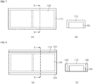
- the substrate 21 may be a growth substrate for growing a III-V nitride based semiconductor layer, for example, a sapphire substrate, and particularly a patterned sapphire substrate.
- the substrate 21 is preferably an insulating substrate, but is not limited to an insulating substrate. However, when light emitting cells disposed on the substrate 21 are connected to each other in series, the substrate 21 must be insulated from the light emitting cells. Therefore, the substrate 21 is insulative, or when the substrate 21 is conductive, an insulation material layer is formed between the light emitting cells C1 and C2 and the substrate 21 for the light emitting cells C1 and C2 to be insulated from the substrate 21.
- the substrate 21 may have a rectangular outer shape as shown in Fig. 1 . A side surface of the substrate 21 may be formed by laser scribing and cracking using the laser scribing.
- the display panel 3210 is not particularly limited and may be, for example, a liquid crystal panel including a liquid crystal layer.
- a gate driving PCB may be further disposed at the periphery of the display panel 3210 to supply driving signals to a gate line.
- the gate driving PCB may be formed on a thin film transistor substrate instead of being formed on a separate PCB.
- the display panel 3210 is secured by the covers 3240, 3280 disposed at upper and lower sides thereof, and the cover 3280 disposed at the lower side of the display panel 3210 may be coupled to the backlight unit.
- the light emitting diodes according to the exemplary embodiments may be applied to headlights like the headlight according to this exemplary embodiment, particularly, vehicular headlights.
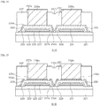
- the mesa M comprises a p-type semiconductor layer 227 and an active layer 225.
- the active layer 225 is interposed between the n-type semiconductor layer 223 and the p-type semiconductor layer 227.
- an inner side surface of the mesa M is shown as being inclined in the same manner as outer side surfaces, the present disclosure is not limited thereto, but the inner side surface of the mesa M may be more gentle than the outer side surfaces. Accordingly, a stability of a second contact layer 235b described later may be improved.
- the reflection structure 231 may comprise a metal layer having reflectivity, or a transparent oxide layer such as ITO(indium tin oxide) or ZnO as described with reference to FIGs. 1 to 4 .
- a preliminary insulation layer 229 may cover the mesa M in a periphery of the reflection structure 231.
- the preliminary insulation layer 229 may be formed of SiO 2 using a chemical vapor deposition technique, for example, and may cover a side of the mesa M and may further cover a partial region of the n-type semiconductor layer 223.
- the preliminary insulation layer 229 may be removed from a lower inclined surface but remain on an upper inclined surface and the stepped surface at the stepped inclined surface of the isolation region I.
- the opening 233c exposes the n-type semiconductor layer 223 in the through-hole 227a and provides a passage for the first contact layer 235a and the second contact layer 235b to be connected to the n-type semiconductor layer 223.
- the first contact layer 235a is disposed on the first light emitting cell C1 and is in ohmic-contact with the n-type semiconductor layer 223.
- the first contact layer 235a may be in ohmic-contact with the n-type semiconductor layer 223 in a region between an outer side surface of the n-type semiconductor layer 223 and the mesa M along the periphery of the mesa M.
- the first contact layer 235a may be in ohmic-contact with the n-type semiconductor layer 223 exposed by the opening 233c of the lower insulation layer 233 in the through-hole 227a of the mesa M.
- the first contact layer 235a may cover the upper region and sides of the mesa M except for a partial region around the hole 233a.
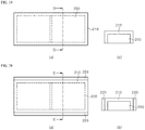
- FIG. 17 is a schematic plan view illustrating a light emitting diode according to another embodiment of the present disclosure.
- the n-electrode pad 239a is divided into two portions and disposed on the first light emitting cell C1, and the p-electrode pad 239a is also divided into two portions and disposed on the second light emitting cell C2.
- the electrode pads 239a and 239b may be divided into a larger number of portions.
- the conductive adhesive such as solder and the like can fill a region between concave portions 237c and the respective portions of the electrode pads 239a and 239b, and thus it is prevented from overflowing to the outside beyond a region of the electrode pads.
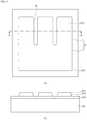
- mesas Ms are formed by patterning the p-type semiconductor layer 227 and the active layer 225.
- the mesas Ms are formed on the respective light emitting cell regions C1 and C2.
- the mesas Ms may be formed using photolithography and etching processes.
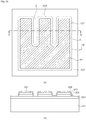
- a preliminary insulation layer 229 which is not shown, is formed to cover the mesas Ms, and then the preliminary insulation layer 229 on a region for forming a reflection structure 231 is etched by using a photoresist pattern. Then, the reflection structure 231 is formed by the lift-off technique using the same photoresist pattern.
- a resin layer 237, an n-electrode pad 239a, and a p-pad electrode 239b are sequentially formed, scribing lines SC1 and SC2 are formed using a laser scribing process.
- the n-electrode pad 239a and the p-electrode pad 239b may be formed to fill a first and second via-holes 237a and 237b in the resin layer 237 using a technique such as electrolytic plating or electroless plating.
- the isolation region ISO is formed between the first and second light emitting cells C1 and C2 in the light emitting diode
- inner side surfaces of the n-type semiconductor layers 223 disposed at positions where the first light emitting cell C1 faces the second light emitting cell C2 are formed to have a relatively gentle slope.
- the outer side surfaces of the n-type semiconductor layers 223 are formed by laser scribing and cracking, they have a relatively steep slope, and further the outer side surfaces of the n-type semiconductor layers 223 may be flush with sides of the substrate 221.
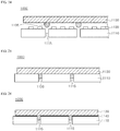
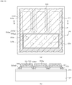
- FIG. 19 is a schematic plan view and a cross-sectional view illustrating a light emitting device comprising a light emitting diode according to an embodiment of the present disclosure
- FIG. 19a is a plan view
- FIG. 19b is a cross-sectional view taken along the line D - D in FIG. 19a .
- the light emitting device according to the present embodiment is substantially similar to the light emitting device described with reference to FIG. 19 , but differs in that reflection sidewalls 220 are disposed along both sides of the light emitting diode 200.
- the reflection sidewalls 220 are disposed along long sides of the light emitting diode 200 and may be omitted on short sides of the light emitting diode 200. Meanwhile, a wavelength conversion layer 210 is disposed between the reflection sidewalls 220 and the light emitting diode 200.
- the reflection sidewalls 220 may be formed by a LED reflector such as PCT, PA9T or SMC (Silicon Molding Compound) and thus may be easily formed using a molding process.
- the light emitting device may be disposed on a side surface of a light guide plate to emit light toward the side surface of the light guide plate, and may be used as a backlight light source, for example.
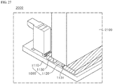
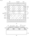
- a light emitting module 1000 comprises a printed circuit board (PCB) 1110, a light emitting device 1120, and a spacer 1130.
- PCB printed circuit board
- the light emitting device 1120 is the same as the light emitting device described with reference to FIG. 19 or FIG. 20 and may be a light emitting device comprising the light emitting diode 200 and the wavelength conversion layer 210, or may be a light emitting diode 200 without the wavelength conversion layer 210.
- a plurality of light emitting devices 1120 are mounted on an upper surface of the printed circuit board 1110. The plurality of light emitting devices 1120 do not need to be all the same, and only a portion of them may comprise the light emitting diodes 200 described above.
- the spacer 1130 is disposed on the upper surface of the printed circuit board 1110.
- a through-hole shaped cavity 1131 is formed in the spacer 1130.
- the cavity 1131 of the spacer 1130 exposes the printed circuit board 1110.
- the light emitting devices 1120 are located inside the cavity 1131 formed in this way.
- a plurality of cavities 1131 are formed in the spacer 1130.
- a plurality of light emitting devices 1120 may be disposed inside of each cavity 1131.
- at least one cavity 1131 of the plurality of cavities 1131 may be different in length from the other cavities 1131.
- at least one cavity 1131 of the plurality of cavities 1131 may be provided with a different number of light emitting devices 1120 from the other cavities 1131.
- the spacer 1130 may be thicker than the light emitting device 1120. That is, an upper surface of the spacer 1130 is located higher than an upper surface of the light emitting device 1120. For example, a thickness of the light emitting device 1120 is 0.4 mm, and a thickness of the spacer 1130 is 0.7 mm.
- the printed circuit board 1110 may be thermally expanded by heat emitted from the light emitting devices 1120, and thus the light emitting devices 1120 may be damaged by touching a light guide plate (not shown).
- the spacer 1130 keeps the light emitting device 1120 away from the light guide plate to prevent the light emitting devices 1120 from being damaged by the light guide plate.
- the cavity 1131 of the spacer 1130 is formed to increase its width from a lower portion to an upper portion. Further, a side surface of the cavity 1131 may be formed as a curved surface. Therefore, light emitted from a side of the light emitting device 1120 may be reflected to a light incident portion of the light guide plate at the side surface of the cavity 1131 (not shown), and thus it is possible to improve light condensing efficiency of the light emitting module 1000.
- One side wall and another side wall of the spacer 1130 may be formed to have different widths.
- one of both side walls formed in a longitudinal direction of the spacer 1130 becomes the one side wall, and the other one becomes the another side wall.
- FIGs. 23 to 26 are cross-sectional views illustrating various methods of attaching spacers.
- the a spacer 1130 may be attached to the printed circuit board 1110 by a protrusion 1135 of the spacer 1130 and a concave portion 1115 of the printed circuit board 1110.
- the spacer 1130 comprises the protrusion 1135.
- the protrusion 1135 is formed on a lower surface of the spacer 1130, and is formed to protrude downward.
- the printed circuit board 1110 comprises the through-hole shaped concave portion 1115.
- the concave portion 1115 is formed at a location corresponding to the protrusion 1135 of the spacer 1130.
- the upper surface of the spacer 1130 is located higher than an upper surface of the light emitting device 1120. Therefore, the spacer 1130 may prevent the light guide plate 2100 from being deformed by heat and damaging the light emitting device 1120.
- FIG. 29 is an enlarged view of a portion indicated by I in FIG. 28
- FIG. 30 is a partial cross-sectional view taken along the line B2 - B2 and a partial cross-sectional view taken along the line C2 - C2 in FIG. 29 .
- the light emitting diode comprises a substrate 321, a first conductivity type semiconductor layer 323, an active layer 325, a second conductivity type semiconductor layer 327, a first contact layer 335a, a second contact layer 331, first insulation layers 329 and 333, an upper insulation layer 337, a first electrode pad 339a, and a second electrode pad 339b.
- the first conductivity type semiconductor layer 321 is disposed on the substrate 321.
- the first conductivity type semiconductor layer 321 is a layer grown on the substrate 321 and is a gallium nitride based semiconductor layer.
- the first conductivity type semiconductor layer 321 may be a gallium nitride based semiconductor layer doped with an impurity, for example, Si.
- the outer contact portion 335a2 and the inner contact portion 335a1 described above may be formed by the opening regions 333a1 and 333a2 formed in the lower insulation layer 333 and the preliminary insulation layer 329.
- the lower insulation layer 333 may also be interposed between the intermediate connection portion 335b and the second contact layer 331, and may have an opening 333b exposing the second contact layer 331.
- the intermediate connection portion 335b may be connected to the second contact layer 331 through these openings 333b.
- FIG. 30 (a) is a cross-sectional view taken along the line B2 - B2 passing through a recess 333r in FIG. 29
- FIG. 30 (b) is a cross-sectional view taken along the line C2 - C2 passing through a protrusion 333p in FIG. 29
- a front line of the first contact layer 335a is located on the protrusion 333p and also contacts the first conductivity type semiconductor layer 323 near the recess 333r.
- the first contact layer 335a contacts the first conductivity type semiconductor layer 323 exposed by the recess 333r and forms the outer contact portion 335a2. Accordingly, the outer contact portions 335a2 and the protrusions 333p alternately contact with the first conductivity type semiconductor layer along the periphery of the mesa M, and thus a contact area of the outer contact portion 335a2 is reduced. Therefore, light loss due to the first contact layer 335a can be reduced.
- the first insulation layers 329 and 333 and the upper insulation layer 337 may be formed of a single layer of SiO 2 , but the present disclosure is not limited thereto.
- the lower insulation layer 333 or the upper insulation layer 337 may have a multiple layer structure comprising a silicon nitride layer and a silicon oxide layer, or may be a distributed Bragg reflector where a silicon oxide layer and a titanium oxide layer are alternately laminated.
- the lower insulation layer 333 is formed of the distributed Bragg reflector with high reflectance, light extraction efficiency may be increased by reflecting light by using the protrusion 333p of the lower insulation layer 333.
- the first electrode pad 339a is electrically connected to the first contact layer 335a through the opening 337a of the upper insulation layer 337
- the second electrode pad 339b is electrically connected to the intermediate connection portion 335b through the opening 337b. Accordingly, the second electrode pad may be electrically connected to the second contact layer 331 via the intermediate connection portion 335b.
- the outer contact portion 335a2 does not continuously contact the first conductivity type semiconductor layer 323 along the periphery of the mesa M, and the outer contact portions 335a2 and first protrusions 333p alternately contact the first conductivity type semiconductor layer along the periphery of the mesa M.
- the technical features are not limited to the present embodiment, but can be similarly applied to the embodiment with the plurality of light emitting cells C1 and C2 described above.
- a first conductivity type semiconductor layer 323, an active layer 325, and a second conductivity type semiconductor layer 327 are grown on a substrate 321.
- the substrate 321 any substrate capable of growing a gallium nitride-based semiconductor layer may be used without limitation.
- the substrate 321 there can be various kinds such as a sapphire substrate, a gallium nitride substrate, a SiC substrate, a Si substrate, or others.
- the first conductivity type semiconductor layer 323, the active layer 325 and the second conductivity type semiconductor layer 327 may be grown on the substrate 321 by Metal Organic Chemical Vapor Deposition (MOCVD).
- MOCVD Metal Organic Chemical Vapor Deposition
- the first conductivity type semiconductor layer 323 may be doped with an n-type impurity, for example, Si.
- the first conductivity type semiconductor layer 323 may have a doping concentration within a range of 8E17/cm 3 to 1E18/cm 3 , for example.
- a side surface of the mesa M may be formed to be inclined by using a process such as photoresist reflow.
- An inclined profile of the side surface of the mesa M improves an extraction efficiency of light generated in the active layer 325.
- a preliminary insulation layer 329 is formed to cover the first conductivity type semiconductor layer 323 and the mesa M.
- the preliminary insulation layer 329 may be formed of SiO 2 using a chemical vapor deposition technique, for example.
- a photoresist pattern 330 is formed on the preliminary insulation layer 329.
- the photoresist pattern 330 has an opening exposing an upper region of the mesa M.
- the opening may be substantially similar to a shape of the mesa M, but may be formed slightly smaller than the mesa M. That is, the photoresist may cover edge portions of the mesa M. Further, the opening may be formed to have larger width of a bottom portion than a width of an inlet. For example, by using a negative type photoresist, the photoresist pattern 330 having an opening with the shape described above may be easily formed.
- the preliminary insulation layer 329 is etched by using the photoresist pattern 330 as an etching mask, and thus the second conductivity type semiconductor layer 327 is exposed.
- the preliminary insulation layer 329 may be etched by using a wet etching technique, for example.
- a second contact layer (e.g., p contact layer 331) is formed.
- the second contact layer 331 may be formed on the mesa M by a coating technique using an electron beam evaporation method.
- the reflection layer may be formed of Ni / Ag / Ni / Au, for example, and the capping layer may cover an upper surface and side surfaces of the reflection layer to protect the reflection layer.
- the reflection layer is formed using an electron beam evaporation method, and the capping layer is formed using a sputtering technique or an electron-beam evaporation method (e.g., planetary e-beam evaporation) in which a layer is vacuum deposited while the substrate 321 is tilted and rotated.
- the capping layer may comprise Ni, Pt, Ti, or Cr, and may be formed by depositing one pair or more of Ni / Pt or one pair or more of of Ni/ Ti, for example.
- the capping layer may comprise TiW, W, or Mo.
- the stress relieving layer is interposed between the reflection layer and the capping layer to relieve stress, and thus may be variously selected depending on metal materials of the reflection layer and the capping layer.
- the stress relieving layer may be a single layer of Ag, Cu, Ni, Pt, Ti, Rh, Pd, or Cr, or may be multiple layers of Cu, Ni, Pt, Ti, Rh, Pd, or Ag.
- the stress relieving layer may be a single layer of Ag or Cu, or multiple layers of Ni, Au, Cu or Ag.
- an antioxidant layer contains Au to prevent oxidation of the capping layer, and may be formed of Au / Ni or Au / Ti, for example. Ti is preferred because of good adhesion of an oxide layer such as SiO2.
- the antioxidant layer may also be formed by using sputtering or electron-beam evaporation (e.g., planetary e-beam evaporation) in which a layer is vacuum deposited while the substrate 321 is tilted and rotated.
- the second contact layer 331 is described as a metal layer, it is not limited thereto, but any material being in ohmic-contact with the second conductivity type semiconductor layer 327 may be used as the second contact layer 331.
- the second contact layer 331 may be a transparent conductive layer such as ITO or ZnO.
- a lower insulation layer 333 covering the mesa M and the first conductivity type semiconductor layer 323 is formed.
- the lower insulation layer 333 covers the second contact layer 331 and also covers the preliminary insulation layer 329. Accordingly, the lower insulation layer 333 is integrated with the insulation layer 329 into one insulation layer and may be patterned together with the insulation layer 329.
- the preliminary insulation layer 329 is formed in advance, but the preliminary insulation layer 329 may be omitted.
- the preliminary insulation layer 329 may be limitedly located on the mesa M. It is not easy to distinguish the preliminary insulation layer 329 from the lower insulation layer 333 because a thickness of the preliminary insulation layer 329 is small. Accordingly, all insulation layers disposed between the mesa M and a first contact layer 335a are referred to as the first insulation layer 329 and 333, unless otherwise noted.
- the first insulation layer 329 and 333 expose the first conductivity type semiconductor layer 323 along a periphery of the mesa M to allow electrical connection to the first conductivity type semiconductor layer 323 in a specific region, and expose the first conductivity type semiconductor layer 323 in a region between the fingers Fs. These opening areas are indicated by reference numerals 333a1 and 333a2. Further, the first insulation layer 329 and 333 have openings 333b to allow electrical connection to the second contact layer 331. The first insulation layer 329 and 333 may have different thicknesses at respective positions depending on whether or not the preliminary insulation layer 329 is present.
- a thickness of the first insulation layer 329 and 333 located on the second contact layer 331 is greater than a thickness of the first insulation layer 329 and 333 located around the second contact layer 331.
- a thickness of the first insulation layer 329 and 333 located around the second contact layer 331 on the mesa M is greater than a thickness of the first insulation layer 333 located on the second contact layer 331 or on the first conductivity type semiconductor layer 323.
- the opening regions 333a1 and 333a2 may be formed by patterning the lower insulation layer 333 and the preliminary insulation layer 329 together, and the opening 333b may be formed by patterning only the lower insulation layer 333 without the preliminary insulation layer 329. Further, the opening 333b is located on the second contact layer 331, and overlaps with the second contact layer 331.
- the opening region 333a2 is determined by a location of a front line of the first insulation layer 329 and 333. That is, the opening region 333a2 between an edge of an upper surface of the first conductivity type semiconductor layer 323 and the front line of the first insulation layer 329 and 333 is exposed.
- the front line of the first insulation layer 329 and 333 comprises protrusions 333p and recesses 333r.
- the front line may have a triangular waveform, for example, it is not limited thereto, but it may have various forms.
- the protrusions 333p and the recesses 333 may be alternately repeated. Accordingly, the opening area 333a2 has a shape in which a large area and a narrow area are repeated.
- opening 333 b is disposed on the palm P of the mesa M.
- a number of openings 333b is not particularly limited, but it may be one or more. Further, when there are a plurality of openings 333b, they may be arranged so as to have a symmetrical structure, but the present disclosure is not limited thereto.
- the lower insulation layer 333 may be formed of an oxide layer such as SiO 2 or others, a nitride layer such as SiNx or others, or an insulating layer of MgF 2 using a chemical vapor deposition (CVD) technique or the like, and may be patterned by using a photolithography and etching technique.
- oxide layer such as SiO 2 or others
- nitride layer such as SiNx or others
- insulating layer of MgF 2 using a chemical vapor deposition (CVD) technique or the like
- the lower insulation layer 333 may be formed of a distributed Bragg reflector (DBR) in which a low refractive index material layer and an high refractive index material layer are alternately laminated.
- DBR distributed Bragg reflector
- an insulating reflection layer having a high reflectance may be formed by laminating layers such as SiO 2 / TiO 2 , SiO 2 / Nb 2 O 5 , or others.
- the first contact layer 335a and an intermediate connection portion 335b are formed on the first insulation layer 329 and 333.
- the first contact layer 335a and the intermediate connection portion 335b may be formed simultaneously with the same material using a lift-off technique, for example.
- the first contact layer 335a covers over most of the first conductivity type semiconductor layer 323 except for a region where the intermediate connection portion 335b is to be formed.
- the first contact layer 335a is insulated from the mesa M and the second contact layer 331 by the first insulation layer 329 and 333.
- the first contact layer 335a has an opening surrounding the intermediate connection portion 335b, and the intermediate connection portion 335b is formed in the opening.
- the first contact layer 335a comprises an inner contact portion 335a1 contacting the first conductivity type semiconductor layer 323 exposed in the opening 333a1 and an outer contact portion 335a2 contacting the first conductivity type semiconductor layer 323 through the opening region 333a2.
- the outer contact portion 335a2 contacts the first conductivity type semiconductor layer 323 near the edge of the first conductivity type semiconductor layer 323 along the periphery of the mesa M.
- a portion of the front line of the first contact layer 335a is located on the protrusions 333p of the first insulation layer 329 and 333 and is separated from the first conductivity type semiconductor layer 323, and another portion is located on the first conductivity type semiconductor layer 323 exposed in the recess portions 333r of the first insulation layer 329 and 333 and forms the outer contact portion 335a2. Therefore, the outer contact portions 335a of the first contact layer 335a alternately contact the first conductivity type semiconductor layer 323 along a side surface of the mesa M with the first insulation layer 329 and 333.
- an opening of the first contact layer 335a is formed to surround the opening 333b of the first insulation layer, for example, the lower insulation layer 333, and the intermediate connection portion 335b covers the opening 333b of the lower insulation layer 333. Therefore, the intermediate connection portion 335b is connected to the second contact layer 331 through the opening 333b of the lower insulation layer 333.
- the intermediate connection portion 335b is also overlapped with and disposed on the second contact layer 331, and particularly may be limitedly located on the palm P of the mesa M.
- the first contact layer 335a is formed over almost an entire region of the first conductivity type semiconductor layer 323 except for openings. Therefore, current may be easily spread through the first contact layer 335a.
- the first contact layers 335a may comprise a highly reflective metal layer such as an Al layer, and the highly reflective metal layer may be formed on an adhesive layer such as Ti, Cr, Ni, or others.
- a protective layer of a single layer or a multilayer structure of Ni, Cr, Au, or others may be formed on the highly reflective metal layer.
- the first contact layer 335a may have a multilayer structure of Cr / Al / Ni / Ti / Ni / Ti / Au / Ti, for example.
- an upper insulation layer 337 is formed on the first contact layer 335a.
- the upper insulation layer 337 has an opening 337a exposing the first contact layer 335a and an opening 337b exposing the intermediate connection portion 335b.
- the opening 337a may be formed to overlap the first contact layer 335a over the fingers Fs of the mesa M, and the opening 337b may be formed on the intermediate contact portion 335b to overlap the second contact layer 331 on the palm P of the mesa M.
- the opening 337b is located to overlap the second contact layer 331, and may have a smaller size than the intermediate connection portion 335b. Therefore, an edge and sidewalls of the intermediate connection portion 335b are covered with the upper insulation layer 337. Further, sidewalls of the opening of the first contact layer 335a are also covered with the upper insulation layer 337.
- the upper insulation layer 337 may be formed of a single layer of a silicon nitride layer or a silicon oxide layer, it is not limited thereto, but may be formed of multiple layers or a distributed Bragg reflector structure.
- the upper insulation layer 337 may cover an inclined surface L1 and may cover side surfaces of the first conductivity type semiconductor layer 323.
- a distance D between first and second electrode pads may be about 80 ⁇ m or more to prevent a short circuit.
- first and second electrode pads 339a and 339b may be formed together using the same process, for example, a lift-off technique.
- FIG. 38 is a schematic plan view illustrating a light emitting diode according to another embodiment of the present disclosure.
- the inner contact portions 335a1 are formed in the indent portions, however, there is a difference in the present embodiment that the inner contact portions 335a1 are in contact with a first conductivity type semiconductor layer 323 exposed in a groove formed in a mesa M.
- the mesa M has the groove passing through the second conductivity type semiconductor layer 327 and the active layer 325 and exposing the first conductivity type semiconductor layer 323.
- the groove is surrounded by the second conductivity type semiconductor layer 327 and the active layer 325, and the inner contact portions 335a1 are in contact with the first conductivity type semiconductor layer 323 exposed in the groove. Therefore, the inner contact portions 335a1 are separated from outer contact portions 335a2.
- the groove may have an H shape comprising two straight lines and a connection line connecting the straight lines.
- the groove may be disposed in a central region of the mesa.
- the inner contact portions 335a1 may be formed in the two straight lines in the H-shaped groove, but the inner contact portions 335a1 may not be formed in the connection line. That is, the first contact layer 335a may be disposed over the connection line, but it may be separated from the first conductivity type semiconductor layer 323 by the first insulation layer 329 and 333.
- At least one of end terminal portions of the groove may have a wider width than other portions of the straight lines. These terminal portions are located near regions, respectively where a first electrode pad 339a and a second electrode pad 339b are located. As shown in FIG. 38 , the first electrode pad 339a may be disposed to overlap with two terminal portions of the terminal portions, and the second electrode pad 339b may be formed to surround the other two terminal portions.
- a shortest distance between the inner contact portions 335a1 and the outer contact portions 335a2 may be the same at any point of the inner contact portions 335a1. Further, a distance between the inner contact portions 335a1 formed on the two straight lines in the H-shaped groove may be the same as the shortest distance between the inner contact portions 335a1 and the outer contact portions 335a2. Therefore, current may be evenly spread over an entire light emitting region.
- FIG. 39 (a) shows that light is mainly emitted from regions of the indent portions where the inner contact portions 335a1 are formed, but light is not emitted well in a region where the second electrode pad 339b is disposed.
- FIG. 39 (b) shows that light is preferably emitted from most of regions of the light emitting surface.
Priority Applications (2)
| Application Number | Priority Date | Filing Date | Title |
|---|---|---|---|
| EP20194164.8A EP3767688B1 (de) | 2016-05-03 | 2017-04-26 | Lichtemittierende diode |
| EP22203445.6A EP4145543A1 (de) | 2016-05-03 | 2017-04-26 | Leuchtdiode |
Applications Claiming Priority (4)
| Application Number | Priority Date | Filing Date | Title |
|---|---|---|---|
| KR1020160054885A KR102495483B1 (ko) | 2016-05-03 | 2016-05-03 | 복수의 발광셀들을 갖는 발광 다이오드 및 그것을 갖는 발광 소자 |
| KR1020160065501A KR102440222B1 (ko) | 2016-05-27 | 2016-05-27 | 발광 다이오드 |
| KR1020160079392A KR102562064B1 (ko) | 2016-06-24 | 2016-06-24 | 복수의 발광셀들을 갖는 발광 다이오드 및 그것을 갖는 발광 모듈 |
| PCT/KR2017/004420 WO2017191923A1 (ko) | 2016-05-03 | 2017-04-26 | 발광 다이오드 |
Related Child Applications (3)
| Application Number | Title | Priority Date | Filing Date |
|---|---|---|---|
| EP22203445.6A Division EP4145543A1 (de) | 2016-05-03 | 2017-04-26 | Leuchtdiode |
| EP20194164.8A Division-Into EP3767688B1 (de) | 2016-05-03 | 2017-04-26 | Lichtemittierende diode |
| EP20194164.8A Division EP3767688B1 (de) | 2016-05-03 | 2017-04-26 | Lichtemittierende diode |
Publications (3)
| Publication Number | Publication Date |
|---|---|
| EP3454372A1 true EP3454372A1 (de) | 2019-03-13 |
| EP3454372A4 EP3454372A4 (de) | 2019-11-20 |
| EP3454372B1 EP3454372B1 (de) | 2020-12-23 |
Family
ID=60202961
Family Applications (3)
| Application Number | Title | Priority Date | Filing Date |
|---|---|---|---|
| EP17792825.6A Active EP3454372B1 (de) | 2016-05-03 | 2017-04-26 | Lichtemittierende diode |
| EP20194164.8A Active EP3767688B1 (de) | 2016-05-03 | 2017-04-26 | Lichtemittierende diode |
| EP22203445.6A Pending EP4145543A1 (de) | 2016-05-03 | 2017-04-26 | Leuchtdiode |
Family Applications After (2)
| Application Number | Title | Priority Date | Filing Date |
|---|---|---|---|
| EP20194164.8A Active EP3767688B1 (de) | 2016-05-03 | 2017-04-26 | Lichtemittierende diode |
| EP22203445.6A Pending EP4145543A1 (de) | 2016-05-03 | 2017-04-26 | Leuchtdiode |
Country Status (4)
| Country | Link |
|---|---|
| US (2) | US10998479B2 (de) |
| EP (3) | EP3454372B1 (de) |
| CN (2) | CN111128987A (de) |
| WO (1) | WO2017191923A1 (de) |
Cited By (4)
| Publication number | Priority date | Publication date | Assignee | Title |
|---|---|---|---|---|
| EP3731277A1 (de) * | 2018-08-09 | 2020-10-28 | Seoul Viosys Co., Ltd | Lichtemittierende vorrichtung |
| WO2021032397A1 (de) * | 2019-08-22 | 2021-02-25 | Osram Opto Semiconductors Gmbh | Optoelektronischer halbleiterchip |
| WO2021032512A1 (de) * | 2019-08-21 | 2021-02-25 | Osram Opto Semiconductors Gmbh | Optoelektronischer halbleiterchip und verfahren zur herstellung eines solchen |
| US10937938B2 (en) | 2018-08-09 | 2021-03-02 | Seoul Viosys Co., Ltd. | Light emitting device |
Families Citing this family (19)
| Publication number | Priority date | Publication date | Assignee | Title |
|---|---|---|---|---|
| CN113345988A (zh) | 2015-10-01 | 2021-09-03 | 克利公司 | 包括倒装芯片发光二极管的发光设备 |
| US11923481B2 (en) | 2018-01-29 | 2024-03-05 | Creeled, Inc. | Reflective layers for light-emitting diodes |
| US11387389B2 (en) | 2018-01-29 | 2022-07-12 | Creeled, Inc. | Reflective layers for light-emitting diodes |
| US11031527B2 (en) | 2018-01-29 | 2021-06-08 | Creeled, Inc. | Reflective layers for light-emitting diodes |
| DE102018107667A1 (de) * | 2018-03-15 | 2019-09-19 | Osram Opto Semiconductors Gmbh | Optoelektronischer halbleiterchip |
| US11799058B2 (en) | 2018-03-15 | 2023-10-24 | Osram Oled Gmbh | Optoelectronic semiconductor chip |
| US10879419B2 (en) * | 2018-08-17 | 2020-12-29 | Seoul Viosys Co., Ltd. | Light emitting device |
| US10879441B2 (en) * | 2018-12-17 | 2020-12-29 | Cree, Inc. | Interconnects for light emitting diode chips |
| US11152553B2 (en) * | 2019-01-15 | 2021-10-19 | Seoul Viosys Co., Ltd. | Light emitting device package and display device having the same |
| US10985294B2 (en) * | 2019-03-19 | 2021-04-20 | Creeled, Inc. | Contact structures for light emitting diode chips |
| CN114583033A (zh) * | 2019-04-08 | 2022-06-03 | 厦门三安光电有限公司 | 一种发光二极管 |
| CN110164322A (zh) * | 2019-05-22 | 2019-08-23 | 深圳市华星光电半导体显示技术有限公司 | 一种显示面板及电子装置 |
| CN111987083A (zh) * | 2019-05-23 | 2020-11-24 | 群创光电股份有限公司 | 电子装置以及发光单元 |
| US11094848B2 (en) | 2019-08-16 | 2021-08-17 | Creeled, Inc. | Light-emitting diode chip structures |
| JP7339517B2 (ja) * | 2019-09-12 | 2023-09-06 | 日亜化学工業株式会社 | 発光装置の製造方法および発光装置 |
| CN113851567B (zh) * | 2021-11-26 | 2022-04-12 | 泉州三安半导体科技有限公司 | 一种发光二极管芯片、发光装置 |
| CN114975721A (zh) * | 2022-05-31 | 2022-08-30 | 京东方科技集团股份有限公司 | 显示面板及其制作方法、以及显示装置 |
| CN115207178B (zh) * | 2022-07-14 | 2023-09-29 | 淮安澳洋顺昌光电技术有限公司 | 一种倒装高压发光二极管 |
| CN116581225B (zh) * | 2023-07-13 | 2023-10-17 | 江西兆驰半导体有限公司 | 一种倒装发光二极管芯片及其制备方法 |
Family Cites Families (26)
| Publication number | Priority date | Publication date | Assignee | Title |
|---|---|---|---|---|
| KR20100003321A (ko) | 2008-06-24 | 2010-01-08 | 삼성전자주식회사 | 발광 소자, 이를 포함하는 발광 장치, 상기 발광 소자 및발광 장치의 제조 방법 |
| JP2011035017A (ja) * | 2009-07-30 | 2011-02-17 | Hitachi Cable Ltd | 発光素子 |
| JP2011066073A (ja) * | 2009-09-15 | 2011-03-31 | Showa Denko Kk | 半導体発光素子 |
| KR20110087579A (ko) * | 2010-01-26 | 2011-08-03 | 삼성엘이디 주식회사 | Led 모듈과 이를 구비하는 백라이트 유닛 |
| US20120037946A1 (en) * | 2010-08-12 | 2012-02-16 | Chi Mei Lighting Technology Corporation | Light emitting devices |
| US9070851B2 (en) * | 2010-09-24 | 2015-06-30 | Seoul Semiconductor Co., Ltd. | Wafer-level light emitting diode package and method of fabricating the same |
| KR101142965B1 (ko) * | 2010-09-24 | 2012-05-08 | 서울반도체 주식회사 | 웨이퍼 레벨 발광 다이오드 패키지 및 그것을 제조하는 방법 |
| KR101106139B1 (ko) * | 2011-04-04 | 2012-01-20 | 서울옵토디바이스주식회사 | 확장된 금속 반사층을 갖는 플립 본딩형 발광다이오드 및 그 제조방법 |
| CN202150484U (zh) * | 2011-05-06 | 2012-02-22 | 福建省万邦光电科技有限公司 | Led光源模块封装用凸杯底座结构 |
| CN103828073B (zh) * | 2011-09-16 | 2016-09-21 | 首尔伟傲世有限公司 | 发光二极管及制造该发光二极管的方法 |
| JP5543514B2 (ja) * | 2012-03-23 | 2014-07-09 | 株式会社東芝 | 半導体発光素子及びその製造方法 |
| KR20140006485A (ko) * | 2012-07-05 | 2014-01-16 | 삼성전자주식회사 | 멀티셀 어레이를 갖는 반도체 발광장치 및 그 제조 방법 |
| KR20140028803A (ko) * | 2012-08-30 | 2014-03-10 | 서울바이오시스 주식회사 | 반사 절연층을 갖는 플립 본딩을 위한 발광다이오드 및 그의 제조방법 |
| CN202839604U (zh) * | 2012-09-22 | 2013-03-27 | 歌尔声学股份有限公司 | 发光二极管装置 |
| KR101420788B1 (ko) * | 2012-12-05 | 2014-07-18 | 주식회사 세미콘라이트 | 반도체 발광소자 |
| US9356212B2 (en) * | 2012-12-21 | 2016-05-31 | Seoul Viosys Co., Ltd. | Light emitting diode and method of fabricating the same |
| US20140362603A1 (en) * | 2013-05-09 | 2014-12-11 | Seoul Semiconductor Co., Ltd. | Light source module and backlight unit having the same |
| WO2015016561A1 (en) * | 2013-07-29 | 2015-02-05 | Seoul Viosys Co., Ltd. | Light emitting diode, method of fabricating the same and led module having the same |
| US9847457B2 (en) * | 2013-07-29 | 2017-12-19 | Seoul Viosys Co., Ltd. | Light emitting diode, method of fabricating the same and LED module having the same |
| US9461209B2 (en) * | 2013-11-27 | 2016-10-04 | Epistar Corporation | Semiconductor light-emitting device |
| US9831387B2 (en) * | 2014-06-14 | 2017-11-28 | Hiphoton Co., Ltd. | Light engine array |
| KR102197082B1 (ko) * | 2014-06-16 | 2020-12-31 | 엘지이노텍 주식회사 | 발광 소자 및 이를 포함하는 발광소자 패키지 |
| US9930750B2 (en) * | 2014-08-20 | 2018-03-27 | Lumens Co., Ltd. | Method for manufacturing light-emitting device packages, light-emitting device package strip, and light-emitting device package |
| WO2016032193A1 (ko) * | 2014-08-27 | 2016-03-03 | 서울바이오시스 주식회사 | 발광 소자 및 이의 제조 방법 |
| KR102335452B1 (ko) * | 2015-06-16 | 2021-12-07 | 서울바이오시스 주식회사 | 발광 소자 |
| WO2017155282A1 (ko) * | 2016-03-07 | 2017-09-14 | 주식회사 세미콘라이트 | 반도체 발광소자 및 이의 제조방법 |
-
2017
- 2017-04-26 WO PCT/KR2017/004420 patent/WO2017191923A1/ko active Application Filing
- 2017-04-26 EP EP17792825.6A patent/EP3454372B1/de active Active
- 2017-04-26 EP EP20194164.8A patent/EP3767688B1/de active Active
- 2017-04-26 EP EP22203445.6A patent/EP4145543A1/de active Pending
- 2017-04-26 CN CN201911378761.XA patent/CN111128987A/zh not_active Withdrawn
- 2017-04-26 CN CN201780024878.0A patent/CN109075184B/zh active Active
-
2018
- 2018-10-12 US US16/158,305 patent/US10998479B2/en active Active
-
2021
- 2021-05-03 US US17/246,856 patent/US20210257528A1/en active Pending
Cited By (4)
| Publication number | Priority date | Publication date | Assignee | Title |
|---|---|---|---|---|
| EP3731277A1 (de) * | 2018-08-09 | 2020-10-28 | Seoul Viosys Co., Ltd | Lichtemittierende vorrichtung |
| US10937938B2 (en) | 2018-08-09 | 2021-03-02 | Seoul Viosys Co., Ltd. | Light emitting device |
| WO2021032512A1 (de) * | 2019-08-21 | 2021-02-25 | Osram Opto Semiconductors Gmbh | Optoelektronischer halbleiterchip und verfahren zur herstellung eines solchen |
| WO2021032397A1 (de) * | 2019-08-22 | 2021-02-25 | Osram Opto Semiconductors Gmbh | Optoelektronischer halbleiterchip |
Also Published As
| Publication number | Publication date |
|---|---|
| EP3454372B1 (de) | 2020-12-23 |
| CN111128987A (zh) | 2020-05-08 |
| US20190051805A1 (en) | 2019-02-14 |
| WO2017191923A1 (ko) | 2017-11-09 |
| CN109075184A (zh) | 2018-12-21 |
| US10998479B2 (en) | 2021-05-04 |
| US20210257528A1 (en) | 2021-08-19 |
| EP4145543A1 (de) | 2023-03-08 |
| EP3767688A1 (de) | 2021-01-20 |
| EP3454372A4 (de) | 2019-11-20 |
| CN109075184B (zh) | 2023-07-21 |
| EP3767688B1 (de) | 2022-10-26 |
Similar Documents
| Publication | Publication Date | Title |
|---|---|---|
| EP3454372B1 (de) | Lichtemittierende diode | |
| KR102641239B1 (ko) | 발광 다이오드, 그것을 제조하는 방법 및 그것을 갖는 발광 소자 모듈 | |
| US9165977B2 (en) | Light emitting device and light emitting device package including series of light emitting regions | |
| US9240433B2 (en) | Light emitting device | |
| EP2372791B1 (de) | Leuchtdiode | |
| US20170236979A1 (en) | Light-emitting element and light-emitting package comprising same | |
| CN110010737B (zh) | 发光器件和照明设备 | |
| US9153622B2 (en) | Series of light emitting regions with an intermediate pad | |
| CN111048547B (zh) | 具有多个发光单元的发光二极管 | |
| CN111164753B (zh) | 半导体装置及包括该半导体装置的前照灯 | |
| KR20160025455A (ko) | 발광 소자 및 이의 제조 방법 | |
| JP2011171743A (ja) | 発光素子及び発光素子パッケージ | |
| KR20140022640A (ko) | 반도체 발광소자 및 발광장치 | |
| KR20160025456A (ko) | 발광 다이오드 및 그 제조 방법 | |
| KR20160149827A (ko) | 복수의 파장변환부를 포함하는 발광 소자 및 그 제조 방법 | |
| EP3471156B1 (de) | Lichtemittierende vorrichtungsverpackung | |
| KR101769048B1 (ko) | 발광 소자, 이를 포함하는 발광소자 패키지 및 조명 장치 | |
| KR100646636B1 (ko) | 발광 소자 및 이의 제조 방법 | |
| KR101221643B1 (ko) | 플립칩 구조의 발광 소자 및 이의 제조 방법 | |
| KR20170082889A (ko) | 발광소자 | |
| KR101115533B1 (ko) | 플립칩 구조의 발광 소자 및 이의 제조 방법 | |
| KR102562064B1 (ko) | 복수의 발광셀들을 갖는 발광 다이오드 및 그것을 갖는 발광 모듈 | |
| KR102475409B1 (ko) | 금속 벌크를 포함하는 발광 소자 | |
| KR101205524B1 (ko) | 플립칩 구조의 발광 소자 및 이의 제조 방법 | |
| KR102170219B1 (ko) | 발광 소자 및 발광 소자 패키지 |
Legal Events
| Date | Code | Title | Description |
|---|---|---|---|
| STAA | Information on the status of an ep patent application or granted ep patent |
Free format text: STATUS: THE INTERNATIONAL PUBLICATION HAS BEEN MADE |
|
| PUAI | Public reference made under article 153(3) epc to a published international application that has entered the european phase |
Free format text: ORIGINAL CODE: 0009012 |
|
| STAA | Information on the status of an ep patent application or granted ep patent |
Free format text: STATUS: REQUEST FOR EXAMINATION WAS MADE |
|
| 17P | Request for examination filed |
Effective date: 20181004 |
|
| AK | Designated contracting states |
Kind code of ref document: A1 Designated state(s): AL AT BE BG CH CY CZ DE DK EE ES FI FR GB GR HR HU IE IS IT LI LT LU LV MC MK MT NL NO PL PT RO RS SE SI SK SM TR |
|
| AX | Request for extension of the european patent |
Extension state: BA ME |
|
| DAV | Request for validation of the european patent (deleted) | ||
| DAX | Request for extension of the european patent (deleted) | ||
| A4 | Supplementary search report drawn up and despatched |
Effective date: 20191017 |
|
| RIC1 | Information provided on ipc code assigned before grant |
Ipc: H01L 33/36 20100101ALI20191011BHEP Ipc: H01L 33/22 20100101ALN20191011BHEP Ipc: H01L 33/38 20100101ALI20191011BHEP Ipc: H01L 33/44 20100101ALI20191011BHEP Ipc: H01L 27/15 20060101ALI20191011BHEP Ipc: H01L 33/46 20100101ALN20191011BHEP Ipc: H01L 33/40 20100101ALI20191011BHEP Ipc: H01L 33/08 20100101AFI20191011BHEP |
|
| REG | Reference to a national code |
Ref country code: DE Ref legal event code: R079 Ref document number: 602017030139 Country of ref document: DE Free format text: PREVIOUS MAIN CLASS: H01L0027150000 Ipc: H01L0033080000 |
|
| GRAP | Despatch of communication of intention to grant a patent |
Free format text: ORIGINAL CODE: EPIDOSNIGR1 |
|
| STAA | Information on the status of an ep patent application or granted ep patent |
Free format text: STATUS: GRANT OF PATENT IS INTENDED |
|
| RIC1 | Information provided on ipc code assigned before grant |
Ipc: H01L 33/46 20100101ALN20200624BHEP Ipc: H01L 27/15 20060101ALI20200624BHEP Ipc: H01L 33/22 20100101ALN20200624BHEP Ipc: H01L 33/40 20100101ALI20200624BHEP Ipc: H01L 33/38 20100101ALI20200624BHEP Ipc: H01L 33/44 20100101ALI20200624BHEP Ipc: H01L 33/08 20100101AFI20200624BHEP Ipc: H01L 33/36 20100101ALI20200624BHEP |
|
| INTG | Intention to grant announced |
Effective date: 20200716 |
|
| GRAS | Grant fee paid |
Free format text: ORIGINAL CODE: EPIDOSNIGR3 |
|
| GRAA | (expected) grant |
Free format text: ORIGINAL CODE: 0009210 |
|
| STAA | Information on the status of an ep patent application or granted ep patent |
Free format text: STATUS: THE PATENT HAS BEEN GRANTED |
|
| AK | Designated contracting states |
Kind code of ref document: B1 Designated state(s): AL AT BE BG CH CY CZ DE DK EE ES FI FR GB GR HR HU IE IS IT LI LT LU LV MC MK MT NL NO PL PT RO RS SE SI SK SM TR |
|
| REG | Reference to a national code |
Ref country code: GB Ref legal event code: FG4D |
|
| REG | Reference to a national code |
Ref country code: DE Ref legal event code: R096 Ref document number: 602017030139 Country of ref document: DE |
|
| REG | Reference to a national code |
Ref country code: AT Ref legal event code: REF Ref document number: 1348565 Country of ref document: AT Kind code of ref document: T Effective date: 20210115 |
|
| REG | Reference to a national code |
Ref country code: IE Ref legal event code: FG4D |
|
| REG | Reference to a national code |
Ref country code: NL Ref legal event code: FP |
|
| PG25 | Lapsed in a contracting state [announced via postgrant information from national office to epo] |
Ref country code: FI Free format text: LAPSE BECAUSE OF FAILURE TO SUBMIT A TRANSLATION OF THE DESCRIPTION OR TO PAY THE FEE WITHIN THE PRESCRIBED TIME-LIMIT Effective date: 20201223 Ref country code: RS Free format text: LAPSE BECAUSE OF FAILURE TO SUBMIT A TRANSLATION OF THE DESCRIPTION OR TO PAY THE FEE WITHIN THE PRESCRIBED TIME-LIMIT Effective date: 20201223 Ref country code: NO Free format text: LAPSE BECAUSE OF FAILURE TO SUBMIT A TRANSLATION OF THE DESCRIPTION OR TO PAY THE FEE WITHIN THE PRESCRIBED TIME-LIMIT Effective date: 20210323 Ref country code: GR Free format text: LAPSE BECAUSE OF FAILURE TO SUBMIT A TRANSLATION OF THE DESCRIPTION OR TO PAY THE FEE WITHIN THE PRESCRIBED TIME-LIMIT Effective date: 20210324 |
|
| REG | Reference to a national code |
Ref country code: AT Ref legal event code: MK05 Ref document number: 1348565 Country of ref document: AT Kind code of ref document: T Effective date: 20201223 |
|
| PG25 | Lapsed in a contracting state [announced via postgrant information from national office to epo] |
Ref country code: SE Free format text: LAPSE BECAUSE OF FAILURE TO SUBMIT A TRANSLATION OF THE DESCRIPTION OR TO PAY THE FEE WITHIN THE PRESCRIBED TIME-LIMIT Effective date: 20201223 Ref country code: LV Free format text: LAPSE BECAUSE OF FAILURE TO SUBMIT A TRANSLATION OF THE DESCRIPTION OR TO PAY THE FEE WITHIN THE PRESCRIBED TIME-LIMIT Effective date: 20201223 Ref country code: BG Free format text: LAPSE BECAUSE OF FAILURE TO SUBMIT A TRANSLATION OF THE DESCRIPTION OR TO PAY THE FEE WITHIN THE PRESCRIBED TIME-LIMIT Effective date: 20210323 |
|
| PG25 | Lapsed in a contracting state [announced via postgrant information from national office to epo] |
Ref country code: HR Free format text: LAPSE BECAUSE OF FAILURE TO SUBMIT A TRANSLATION OF THE DESCRIPTION OR TO PAY THE FEE WITHIN THE PRESCRIBED TIME-LIMIT Effective date: 20201223 |
|
| REG | Reference to a national code |
Ref country code: LT Ref legal event code: MG9D |
|
| PG25 | Lapsed in a contracting state [announced via postgrant information from national office to epo] |
Ref country code: LT Free format text: LAPSE BECAUSE OF FAILURE TO SUBMIT A TRANSLATION OF THE DESCRIPTION OR TO PAY THE FEE WITHIN THE PRESCRIBED TIME-LIMIT Effective date: 20201223 Ref country code: CZ Free format text: LAPSE BECAUSE OF FAILURE TO SUBMIT A TRANSLATION OF THE DESCRIPTION OR TO PAY THE FEE WITHIN THE PRESCRIBED TIME-LIMIT Effective date: 20201223 Ref country code: EE Free format text: LAPSE BECAUSE OF FAILURE TO SUBMIT A TRANSLATION OF THE DESCRIPTION OR TO PAY THE FEE WITHIN THE PRESCRIBED TIME-LIMIT Effective date: 20201223 Ref country code: SM Free format text: LAPSE BECAUSE OF FAILURE TO SUBMIT A TRANSLATION OF THE DESCRIPTION OR TO PAY THE FEE WITHIN THE PRESCRIBED TIME-LIMIT Effective date: 20201223 Ref country code: RO Free format text: LAPSE BECAUSE OF FAILURE TO SUBMIT A TRANSLATION OF THE DESCRIPTION OR TO PAY THE FEE WITHIN THE PRESCRIBED TIME-LIMIT Effective date: 20201223 Ref country code: PT Free format text: LAPSE BECAUSE OF FAILURE TO SUBMIT A TRANSLATION OF THE DESCRIPTION OR TO PAY THE FEE WITHIN THE PRESCRIBED TIME-LIMIT Effective date: 20210423 Ref country code: SK Free format text: LAPSE BECAUSE OF FAILURE TO SUBMIT A TRANSLATION OF THE DESCRIPTION OR TO PAY THE FEE WITHIN THE PRESCRIBED TIME-LIMIT Effective date: 20201223 |
|
| PG25 | Lapsed in a contracting state [announced via postgrant information from national office to epo] |
Ref country code: AT Free format text: LAPSE BECAUSE OF FAILURE TO SUBMIT A TRANSLATION OF THE DESCRIPTION OR TO PAY THE FEE WITHIN THE PRESCRIBED TIME-LIMIT Effective date: 20201223 Ref country code: PL Free format text: LAPSE BECAUSE OF FAILURE TO SUBMIT A TRANSLATION OF THE DESCRIPTION OR TO PAY THE FEE WITHIN THE PRESCRIBED TIME-LIMIT Effective date: 20201223 |
|
| REG | Reference to a national code |
Ref country code: DE Ref legal event code: R097 Ref document number: 602017030139 Country of ref document: DE |
|
| PG25 | Lapsed in a contracting state [announced via postgrant information from national office to epo] |
Ref country code: IS Free format text: LAPSE BECAUSE OF FAILURE TO SUBMIT A TRANSLATION OF THE DESCRIPTION OR TO PAY THE FEE WITHIN THE PRESCRIBED TIME-LIMIT Effective date: 20210423 |
|
| PG25 | Lapsed in a contracting state [announced via postgrant information from national office to epo] |
Ref country code: AL Free format text: LAPSE BECAUSE OF FAILURE TO SUBMIT A TRANSLATION OF THE DESCRIPTION OR TO PAY THE FEE WITHIN THE PRESCRIBED TIME-LIMIT Effective date: 20201223 |
|
| PLBE | No opposition filed within time limit |
Free format text: ORIGINAL CODE: 0009261 |
|
| STAA | Information on the status of an ep patent application or granted ep patent |
Free format text: STATUS: NO OPPOSITION FILED WITHIN TIME LIMIT |
|
| PG25 | Lapsed in a contracting state [announced via postgrant information from national office to epo] |
Ref country code: MC Free format text: LAPSE BECAUSE OF FAILURE TO SUBMIT A TRANSLATION OF THE DESCRIPTION OR TO PAY THE FEE WITHIN THE PRESCRIBED TIME-LIMIT Effective date: 20201223 Ref country code: DK Free format text: LAPSE BECAUSE OF FAILURE TO SUBMIT A TRANSLATION OF THE DESCRIPTION OR TO PAY THE FEE WITHIN THE PRESCRIBED TIME-LIMIT Effective date: 20201223 |
|
| 26N | No opposition filed |
Effective date: 20210924 |
|
| PG25 | Lapsed in a contracting state [announced via postgrant information from national office to epo] |
Ref country code: LU Free format text: LAPSE BECAUSE OF NON-PAYMENT OF DUE FEES Effective date: 20210426 |
|
| REG | Reference to a national code |
Ref country code: BE Ref legal event code: MM Effective date: 20210430 |
|
| PG25 | Lapsed in a contracting state [announced via postgrant information from national office to epo] |
Ref country code: ES Free format text: LAPSE BECAUSE OF FAILURE TO SUBMIT A TRANSLATION OF THE DESCRIPTION OR TO PAY THE FEE WITHIN THE PRESCRIBED TIME-LIMIT Effective date: 20201223 Ref country code: CH Free format text: LAPSE BECAUSE OF NON-PAYMENT OF DUE FEES Effective date: 20210430 Ref country code: LI Free format text: LAPSE BECAUSE OF NON-PAYMENT OF DUE FEES Effective date: 20210430 |
|
| PG25 | Lapsed in a contracting state [announced via postgrant information from national office to epo] |
Ref country code: SI Free format text: LAPSE BECAUSE OF FAILURE TO SUBMIT A TRANSLATION OF THE DESCRIPTION OR TO PAY THE FEE WITHIN THE PRESCRIBED TIME-LIMIT Effective date: 20201223 |
|
| PG25 | Lapsed in a contracting state [announced via postgrant information from national office to epo] |
Ref country code: IE Free format text: LAPSE BECAUSE OF NON-PAYMENT OF DUE FEES Effective date: 20210426 |
|
| PG25 | Lapsed in a contracting state [announced via postgrant information from national office to epo] |
Ref country code: IS Free format text: LAPSE BECAUSE OF FAILURE TO SUBMIT A TRANSLATION OF THE DESCRIPTION OR TO PAY THE FEE WITHIN THE PRESCRIBED TIME-LIMIT Effective date: 20210423 |
|
| PG25 | Lapsed in a contracting state [announced via postgrant information from national office to epo] |
Ref country code: BE Free format text: LAPSE BECAUSE OF NON-PAYMENT OF DUE FEES Effective date: 20210430 |
|
| PGFP | Annual fee paid to national office [announced via postgrant information from national office to epo] |
Ref country code: FR Payment date: 20230306 Year of fee payment: 7 |
|
| PGFP | Annual fee paid to national office [announced via postgrant information from national office to epo] |
Ref country code: IT Payment date: 20230309 Year of fee payment: 7 |
|
| PG25 | Lapsed in a contracting state [announced via postgrant information from national office to epo] |
Ref country code: CY Free format text: LAPSE BECAUSE OF FAILURE TO SUBMIT A TRANSLATION OF THE DESCRIPTION OR TO PAY THE FEE WITHIN THE PRESCRIBED TIME-LIMIT Effective date: 20201223 |
|
| PG25 | Lapsed in a contracting state [announced via postgrant information from national office to epo] |
Ref country code: HU Free format text: LAPSE BECAUSE OF FAILURE TO SUBMIT A TRANSLATION OF THE DESCRIPTION OR TO PAY THE FEE WITHIN THE PRESCRIBED TIME-LIMIT; INVALID AB INITIO Effective date: 20170426 |
|
| PGFP | Annual fee paid to national office [announced via postgrant information from national office to epo] |
Ref country code: DE Payment date: 20230306 Year of fee payment: 7 |
|
| PGFP | Annual fee paid to national office [announced via postgrant information from national office to epo] |
Ref country code: NL Payment date: 20240306 Year of fee payment: 8 |
|
| PG25 | Lapsed in a contracting state [announced via postgrant information from national office to epo] |
Ref country code: MK Free format text: LAPSE BECAUSE OF FAILURE TO SUBMIT A TRANSLATION OF THE DESCRIPTION OR TO PAY THE FEE WITHIN THE PRESCRIBED TIME-LIMIT Effective date: 20201223 |
|
| PGFP | Annual fee paid to national office [announced via postgrant information from national office to epo] |
Ref country code: GB Payment date: 20240305 Year of fee payment: 8 |