EP3450196B1 - Anzeigekörper und beobachtungsverfahren für den anzeigekörper - Google Patents
Anzeigekörper und beobachtungsverfahren für den anzeigekörper Download PDFInfo
- Publication number
- EP3450196B1 EP3450196B1 EP18202229.3A EP18202229A EP3450196B1 EP 3450196 B1 EP3450196 B1 EP 3450196B1 EP 18202229 A EP18202229 A EP 18202229A EP 3450196 B1 EP3450196 B1 EP 3450196B1
- Authority
- EP
- European Patent Office
- Prior art keywords
- display
- information
- light
- metal layer
- protrusions
- Prior art date
- Legal status (The legal status is an assumption and is not a legal conclusion. Google has not performed a legal analysis and makes no representation as to the accuracy of the status listed.)
- Active
Links
- 238000000034 method Methods 0.000 title claims description 40
- 229910052751 metal Inorganic materials 0.000 claims description 116
- 239000002184 metal Substances 0.000 claims description 116
- 239000000463 material Substances 0.000 claims description 20
- 239000003086 colorant Substances 0.000 claims description 16
- 230000008859 change Effects 0.000 claims description 13
- RKTYLMNFRDHKIL-UHFFFAOYSA-N copper;5,10,15,20-tetraphenylporphyrin-22,24-diide Chemical compound [Cu+2].C1=CC(C(=C2C=CC([N-]2)=C(C=2C=CC=CC=2)C=2C=CC(N=2)=C(C=2C=CC=CC=2)C2=CC=C3[N-]2)C=2C=CC=CC=2)=NC1=C3C1=CC=CC=C1 RKTYLMNFRDHKIL-UHFFFAOYSA-N 0.000 claims description 8
- 230000002093 peripheral effect Effects 0.000 claims description 8
- 230000001678 irradiating effect Effects 0.000 claims description 3
- 239000011159 matrix material Substances 0.000 claims description 3
- 239000000758 substrate Substances 0.000 description 30
- 230000004048 modification Effects 0.000 description 18
- 238000012986 modification Methods 0.000 description 18
- 229920003023 plastic Polymers 0.000 description 15
- 230000008901 benefit Effects 0.000 description 14
- 230000003287 optical effect Effects 0.000 description 9
- 230000008569 process Effects 0.000 description 8
- 238000010586 diagram Methods 0.000 description 6
- 238000007740 vapor deposition Methods 0.000 description 6
- 238000005240 physical vapour deposition Methods 0.000 description 5
- 230000007423 decrease Effects 0.000 description 4
- 239000004033 plastic Substances 0.000 description 4
- 238000005516 engineering process Methods 0.000 description 3
- 230000001788 irregular Effects 0.000 description 3
- 239000002245 particle Substances 0.000 description 3
- 230000015572 biosynthetic process Effects 0.000 description 2
- 239000000428 dust Substances 0.000 description 2
- 238000005530 etching Methods 0.000 description 2
- 230000005284 excitation Effects 0.000 description 2
- 229910010272 inorganic material Inorganic materials 0.000 description 2
- 239000011147 inorganic material Substances 0.000 description 2
- 239000010453 quartz Substances 0.000 description 2
- VYPSYNLAJGMNEJ-UHFFFAOYSA-N silicon dioxide Inorganic materials O=[Si]=O VYPSYNLAJGMNEJ-UHFFFAOYSA-N 0.000 description 2
- 238000004544 sputter deposition Methods 0.000 description 2
- GWEVSGVZZGPLCZ-UHFFFAOYSA-N Titan oxide Chemical compound O=[Ti]=O GWEVSGVZZGPLCZ-UHFFFAOYSA-N 0.000 description 1
- NRTOMJZYCJJWKI-UHFFFAOYSA-N Titanium nitride Chemical compound [Ti]#N NRTOMJZYCJJWKI-UHFFFAOYSA-N 0.000 description 1
- 229910052782 aluminium Inorganic materials 0.000 description 1
- XAGFODPZIPBFFR-UHFFFAOYSA-N aluminium Chemical compound [Al] XAGFODPZIPBFFR-UHFFFAOYSA-N 0.000 description 1
- 238000003486 chemical etching Methods 0.000 description 1
- 238000009792 diffusion process Methods 0.000 description 1
- PCHJSUWPFVWCPO-UHFFFAOYSA-N gold Chemical compound [Au] PCHJSUWPFVWCPO-UHFFFAOYSA-N 0.000 description 1
- 229910052737 gold Inorganic materials 0.000 description 1
- 239000010931 gold Substances 0.000 description 1
- 238000007646 gravure printing Methods 0.000 description 1
- ORUIBWPALBXDOA-UHFFFAOYSA-L magnesium fluoride Chemical compound [F-].[F-].[Mg+2] ORUIBWPALBXDOA-UHFFFAOYSA-L 0.000 description 1
- 229910001635 magnesium fluoride Inorganic materials 0.000 description 1
- 238000007645 offset printing Methods 0.000 description 1
- 239000011368 organic material Substances 0.000 description 1
- 239000000049 pigment Substances 0.000 description 1
- 238000007639 printing Methods 0.000 description 1
- 230000000452 restraining effect Effects 0.000 description 1
- 238000007650 screen-printing Methods 0.000 description 1
- 229910052709 silver Inorganic materials 0.000 description 1
- 239000004332 silver Substances 0.000 description 1
- 230000003746 surface roughness Effects 0.000 description 1
- OGIDPMRJRNCKJF-UHFFFAOYSA-N titanium oxide Inorganic materials [Ti]=O OGIDPMRJRNCKJF-UHFFFAOYSA-N 0.000 description 1
- 238000002834 transmittance Methods 0.000 description 1
Images


Classifications
-
- G—PHYSICS
- G09—EDUCATION; CRYPTOGRAPHY; DISPLAY; ADVERTISING; SEALS
- G09F—DISPLAYING; ADVERTISING; SIGNS; LABELS OR NAME-PLATES; SEALS
- G09F3/00—Labels, tag tickets, or similar identification or indication means; Seals; Postage or like stamps
- G09F3/02—Forms or constructions
- G09F3/0291—Labels or tickets undergoing a change under particular conditions, e.g. heat, radiation, passage of time
- G09F3/0294—Labels or tickets undergoing a change under particular conditions, e.g. heat, radiation, passage of time where the change is not permanent, e.g. labels only readable under a special light, temperature indicating labels and the like
-
- B—PERFORMING OPERATIONS; TRANSPORTING
- B42—BOOKBINDING; ALBUMS; FILES; SPECIAL PRINTED MATTER
- B42D—BOOKS; BOOK COVERS; LOOSE LEAVES; PRINTED MATTER CHARACTERISED BY IDENTIFICATION OR SECURITY FEATURES; PRINTED MATTER OF SPECIAL FORMAT OR STYLE NOT OTHERWISE PROVIDED FOR; DEVICES FOR USE THEREWITH AND NOT OTHERWISE PROVIDED FOR; MOVABLE-STRIP WRITING OR READING APPARATUS
- B42D25/00—Information-bearing cards or sheet-like structures characterised by identification or security features; Manufacture thereof
- B42D25/20—Information-bearing cards or sheet-like structures characterised by identification or security features; Manufacture thereof characterised by a particular use or purpose
- B42D25/23—Identity cards
-
- B—PERFORMING OPERATIONS; TRANSPORTING
- B42—BOOKBINDING; ALBUMS; FILES; SPECIAL PRINTED MATTER
- B42D—BOOKS; BOOK COVERS; LOOSE LEAVES; PRINTED MATTER CHARACTERISED BY IDENTIFICATION OR SECURITY FEATURES; PRINTED MATTER OF SPECIAL FORMAT OR STYLE NOT OTHERWISE PROVIDED FOR; DEVICES FOR USE THEREWITH AND NOT OTHERWISE PROVIDED FOR; MOVABLE-STRIP WRITING OR READING APPARATUS
- B42D25/00—Information-bearing cards or sheet-like structures characterised by identification or security features; Manufacture thereof
- B42D25/30—Identification or security features, e.g. for preventing forgery
- B42D25/324—Reliefs
-
- B—PERFORMING OPERATIONS; TRANSPORTING
- B42—BOOKBINDING; ALBUMS; FILES; SPECIAL PRINTED MATTER
- B42D—BOOKS; BOOK COVERS; LOOSE LEAVES; PRINTED MATTER CHARACTERISED BY IDENTIFICATION OR SECURITY FEATURES; PRINTED MATTER OF SPECIAL FORMAT OR STYLE NOT OTHERWISE PROVIDED FOR; DEVICES FOR USE THEREWITH AND NOT OTHERWISE PROVIDED FOR; MOVABLE-STRIP WRITING OR READING APPARATUS
- B42D25/00—Information-bearing cards or sheet-like structures characterised by identification or security features; Manufacture thereof
- B42D25/30—Identification or security features, e.g. for preventing forgery
- B42D25/351—Translucent or partly translucent parts, e.g. windows
-
- B—PERFORMING OPERATIONS; TRANSPORTING
- B42—BOOKBINDING; ALBUMS; FILES; SPECIAL PRINTED MATTER
- B42D—BOOKS; BOOK COVERS; LOOSE LEAVES; PRINTED MATTER CHARACTERISED BY IDENTIFICATION OR SECURITY FEATURES; PRINTED MATTER OF SPECIAL FORMAT OR STYLE NOT OTHERWISE PROVIDED FOR; DEVICES FOR USE THEREWITH AND NOT OTHERWISE PROVIDED FOR; MOVABLE-STRIP WRITING OR READING APPARATUS
- B42D25/00—Information-bearing cards or sheet-like structures characterised by identification or security features; Manufacture thereof
- B42D25/30—Identification or security features, e.g. for preventing forgery
- B42D25/36—Identification or security features, e.g. for preventing forgery comprising special materials
- B42D25/373—Metallic materials
Definitions
- the technology of the present disclosure relates to a display body using surface plasmons and a method for observing a display body.
- a display body for displaying image information by using a plurality of cells formed by diffraction grating As a display body that is difficult to counterfeit, there is known a display body for displaying image information by using a plurality of cells formed by diffraction grating. With respect to such a display body, there is also known a display body having a micro-image that corresponds to a bitmap pattern having two or more values inside a specific cell among a plurality of cells and can be observed by using a microscope (refer to, for example, Patent Document 1).
- a micro-image corresponding to a bitmap pattern having two or more values displays an image by two or more height differences. For this reason, for example, when dust or a stain having the same size as the height difference constituting the micro-image overlaps with a part of the micro-image, there is a possibility that an observer of a display body falsely recognizes the dust or stain as a part of the micro-image.
- the technology of the present disclosure is to provide a display body capable of restraining information false recognition of an observer and a method for observing a display body.
- a display body that includes a first display part, which displays first information, and a second display part, which displays second information having a display size greater than that of the first information.
- the second display part includes the entire first display part as a part of the second display part.
- the first display part includes a plasmon structure.
- the plasmon structure is configured to include an interface between a metal layer and a dielectric layer that transmits light, excite surface plasmons in the interface to change irradiation light with which the interface is irradiated to transmitted light having a color different from that of the irradiation light, and display the first information with the transmitted light.
- a method for observing a display body includes a first display part, which displays first information, and a second display part, which displays second information having a display size greater than that of the first information.
- the second display part includes the entire first display part as a part of the second display part.
- the first display part includes a plasmon structure.
- the plasmon structure is configured to include an interface between a metal layer and a dielectric layer that transmits light, excite surface plasmons in the interface to change irradiation light with which the interface is irradiated to transmitted light having a color different from that of the irradiation light, and display the first information with the transmitted light.
- the method includes irradiating the interface of the display body with the irradiation light and observing the display body irradiated with the irradiation light in a magnifying manner.
- the observer of the display body since the first display part included in the second display part displays the first information with the transmitted light having a predetermined color, the observer of the display body can recognize the first information by using the difference between the light having a predetermined color and the other parts. Therefore, the difference between a part for the first information and the other parts can be easily recognized. As a result, false recognition of information by the observer is restrained.
- a display body and a method for observing the display body according to one embodiment of the present disclosure will now be described with reference to Figs. 1 to 7 .
- the overall configuration of a display body, the configuration of a micro-display part included in the display body, the configuration of a display element, functions of the micro-display part, and a method for observing the display body will be sequentially described.
- Fig. 1B is a diagram illustrating a part surrounded by a circle indicated by a long dashed short dashed line of Fig. 1A in a magnified manner.
- a display body 10 is configured to include a substrate 11, a display part 12 located on one surface of the substrate 11, and a plurality of micro-display parts located on one surface of the substrate 11.
- the substrate 11 has, for example, a rectangular plate shape. However, if the substrate has an area where the display part 12 can be located, the shape thereof is not limited to the rectangular plate shape, but the substrate may have other shapes such as a circular plate shape or a rectangular parallelepiped shape.
- the display part 12 is an example of a second display part and displays second information, which is predetermined information.
- Information displayed by the display part 12 is, for example, an image, and as illustrated in Fig. 1A , a shape in which two adjacent circles among three circles are continuous with each other is an example of the image.
- the image, as information displayed by the display part 12, is not limited to figures such as design patterns or shapes, but the image may be characters, symbols, and numerals or may be a combination of at least two of figures, characters, symbols, and numerals.
- the information displayed by the display part 12 is not limited to an image, but the information may be color information such as the ratio of a specific color to the entire display part 12, a color arrangement of the display part 12, or the existence of a color, or may be position information such as a position where a specific color is arranged or a position where a color is added in the display part 12.
- the display part 12 includes the entirety of each micro-display part 13 as a part of the display part 12. That is, the display part 12 is larger than each micro-display part 13 and has a size capable of including the micro-display parts 13 as a part.
- the display part 12 may be a part displaying information by using light diffraction by a diffraction grating structure or may be a part of a metal layer formed on the surface of the substrate 11 having a predetermined shape that is formed by, for example, an etching method, in which information is displayed by light reflection or diffusion on the metal layer.
- Each micro-display part 13 is an example of a first display part.
- the micro-display part 13 has a plasmon structure of exciting surface plasmons to change irradiation light with which the micro-display part 13 is irradiated to transmitted light having a color different from that of the irradiation light.
- the micro-display parts 13 are located within the display part 12.
- the display body 10 does not necessarily need to include the micro-display parts 13, but it may include only one micro-display part 13.
- Each micro-display part 13 displays first information, which is predetermined information and has a display size smaller than that of the second information displayed by the display part 12, by the aforementioned transmitted light. That is, the display size of the second information displayed by the display part 12 may be greater than that of the first information displayed by the micro-display part 13, and the size of the display part 12 may be equal to the display size of the second information. For example, in a case in which the display part 12 displays a three-dimensional image, the size of the display part may be greater or smaller than the display size of the second information.
- the size of the micro-display part 13 may also be equal to the display size of the first information or may be larger or smaller than the display size of the first information.
- the first information is, for example, a predetermined character line as an example of the image.
- the first information displayed by the micro-display part 13 may be an image, color information, or position information.
- each micro-display part 13 is included as a part of the display part 12. That is, the micro-display part 13 is smaller than the display part 12 and has a size capable of being included within the display part 12.
- the micro-display parts 13 may be arranged regularly or irregularly within the display part 12.
- micro-display part 13 A more detailed configuration of the micro-display part 13 will now be described with reference to Fig. 2 .
- the micro-display part 13 is configured to include a plurality of display elements 21 arranged in a matrix shape.
- Each display element 21 is a region having, for example, a rectangular shape defined inside the display part 12.
- the display element 21 is not limited to the rectangular shape, but it may be a region having, for example, various polygon shapes other than the rectangular shape, such as a triangular shape or a pentagonal shape.
- the first information displayed by the micro-display part 13 is configured with a plurality of information elements, and the micro-display part 13 is configured to include display elements 21 for respective information elements.
- the length L1 of one side of each display element 21 is, for example, 200 nm or more and 3000 nm or less. If the length L1 of one side of the display element 21 is 200 nm or more and 3000 nm or less, the size of the display element 21 is a preferred size so that the micro-display part 13 is difficult to visually recognize and the micro-display part 13 can be observed at a magnification ratio settable in an optical microscope.
- the display elements 21 are arranged along a row direction R as one direction and are arranged along a column direction C perpendicular to the row direction R.
- the number of display elements 21 arranged in the row direction R is, for example, 10 or more and 100 or less
- the number of display elements 21 arranged in the column direction C is, for example, 10 or more and 100 or less.
- one micro-display part 13 is configured to include 100 or more and 10000 or less of the display elements 21.
- the size of the micro-display part 13 is a preferred size in terms of the following point. That is, the size of the micro-display part 13 is a preferred size so that the micro-display part 13 is difficult to visually recognize and the micro-display part 13 can be observed at a magnification ratio settable in an optical microscope.
- the first information displayed by each micro-display part 13 includes a plurality of information elements including a first information element representing a first color and a second information element representing a second color different from the first color.
- the display elements 21 constituting the micro-display part 13 include a first display element 22 corresponding to the first information element representing the first color and a second display element 23 corresponding to the second information element representing the second color.
- the plasmon structure included in the first display element 22 and the plasmon structure included in the second display element 23 transmit light having different colors.
- each micro-display part 13 for example, the first display elements 22 display a Roman letter O, and the second display elements 23 display a Roman letter K.
- the micro-display part 13 displays a red Roman letter O as a part of the first information.
- the micro-display part 13 displays a blue Roman letter K as a part of the first information.
- Each micro-display part 13 further includes a plurality of peripheral elements 24 including a part between the first display elements 22 and the second display elements 23, a part surrounded by the first display elements 22, or a part surrounded by the second display elements 23.
- Each of the peripheral elements 24 may be a part that transmits the irradiation light with which the micro-display part 13 is irradiated without change in color of the irradiation light, may be a part that does not transmit the irradiation light, or may be a part that transmits light having a color different from those of the first display element 22 and the second display element 23.
- Each micro-display part 13 does not necessarily need to include the peripheral elements 24.
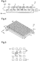
- FIG. 21 A detailed configuration of the display element 21 will now be described with reference to Figs. 3 to 5 .
- the display elements 21 having plasmon structures like the first display element 22 and the second display element 23 will now be described.
- the display element 21 has a plasmon structure configured to include a metal layer 31, a dielectric layer 32, which transmits light, and an interface 33 between the metal layer 31 and the dielectric layer 32.
- the plasmon structure of the display element 21 excites surface plasmons in an interface 33 by the irradiation light with which the interface between the dielectric layer 32 and the metal layer 31 is irradiated to change the irradiation light to light having a color different from that of the irradiation light.
- the dielectric layer 32 includes, for example, a base body 41 having a base surface 41a as one surface, and the base body 41 includes a plurality of protrusions 42, which protrude from the base surface 41a.
- the base surface 41a is a formation surface on which the protrusions 42 are formed.
- the dielectric layer 32 may have a multi-layered structure including layers other than the base body 41. In each protrusion 42, a surface farther from the base surface 41a is a top surface 42a, and a surface including the top surfaces 42a of all the protrusions 42 is an imaginary plane 42b.
- the base surface 41a of the base body 41 and the imaginary plane 42b are substantially parallel to each other.
- the distance D between the base surface 41a and the imaginary plane 42b is preferably, for example, 30 nm or more and 500 nm or less.
- the plasmon structure included in the display element 21 preferably has at least one interface 33 between the metal layer 31 and the dielectric layer 32. Therefore, the plasmon structure excites surface plasmons in the interface 33 by the irradiation light with which the interface 33 is irradiated to change the irradiation light to transmitted light having a color different from that of the irradiation light.
- the plasmon structure included in one display element 21 preferably has a configuration in which one display element 21 transmits transmitted light having a predetermined color and in which the plasmon structure includes two or more protrusions 42 and a metal layer 31 covering at least the top surface 42a of each protrusion 42.
- each protrusion 42 has, for example, a rectangular pillar shape.
- each protrusion may have a polygonal pillar shape other than the rectangular pillar shape such as a trigonal pillar shape or a pentagonal pillar shape, may have a cylindrical shape or an elliptic cylindrical shape, or may have a conical shape such as a cone shape or a polygonal pyramid shape.
- each protrusion 42 may have a polygonal pillar shape, each of the corners of the polygonal pillar shape may have a curvature.
- each protrusion 42 may have a plurality of step differences at a side surface connecting the top surface 42a and the base surface 41a.
- each protrusion 42 may have a shape in which, in a step difference surface including a surface substantially parallel to the imaginary plane 42b and in a cross section along a direction of the thickness T of the metal layer 31 of each protrusion 42, a width thereof in a direction perpendicular to an extension direction of the protrusion 42 is increased for every step difference from the top surface 42a toward the base surface 41a.
- the metal layer 31 may be located on each surface substantially parallel to the imaginary plane 42b in the side surface.
- the material for forming the dielectric layer 32 is, for example, quartz.
- an inorganic material transmitting visible light other than quartz for example, a titanium oxide or a magnesium fluoride may be used, or an organic material transmitting visible light, for example, various plastics may be used.
- the dielectric layer 32 including the base body 41 and the protrusions 42 included in the base body 41 is formed, for example, by applying a chemical etching process, a physical etching process, or the like on a substrate formed by each material.
- the dielectric layer 32 including the base body 41 and the protrusions 42 included in the base body 41 is formed, for example, by transferring an original plate to a layer formed with the plastic.
- the dielectric layer 32 constitutes a part of the substrate 11 in the display body 10.
- the entire substrate 11 may be formed with the same material as the material for forming the dielectric layer 32, or the substrate 11 may include the dielectric layer 32 and a portion formed with a material different from the material for forming the dielectric layer 32.
- the metal layer 31 may be formed, for example, on the entire part in which the protrusions 42 are not formed on the base surface 41a, and on the top surfaces 42a of the protrusions 42.
- the metal layer 31 may be formed on a part of the base surface 41a, may be formed on a part of each top surface 42a, may be formed only on the base surface 41a, or may be only on the top surface 42a. Therefore, the interface 33 between the dielectric layer 32 and the metal layer 31 is formed.
- the thickness T of the metal layer 31 is, for example, 20 nm or more and 100 nm or less, preferably, 40 nm or more and 60 nm or less.
- the material for forming the metal layer 31 is, for example, aluminum.
- the material for forming the metal layer 31 may be gold, silver, a titanium nitride, or the like, and the real part of the complex dielectric constant of the forming material in a visible light range preferably has a negative value.
- the material for forming the metal layer 31 has such characteristics, the light transmitted by the excitation of the surface plasmons is reliably included in the visible light range. For this reason, an observer can reliably recognize the information displayed by the display body 10.
- the metal layer 31 is formed, for example, by a physical vapor deposition method such as a vacuum vapor deposition method or a sputtering method.
- a vacuum vapor deposition method When the metal layer 31 is formed by a vacuum vapor deposition method, a fine uneven structure is formed on the surface of the metal layer 31.
- the fine uneven structure formed by the vacuum vapor deposition method has a size to such an extent that the fine uneven structure does not influence the state of the surface plasmons formed in the interface 33 between the metal layer 31 and the dielectric layer 32. For this reason, the metal layer 31 may have such an uneven structure, that is, surface roughness, to the extent that the uneven structure is formed by the vacuum vapor deposition method.
- a plurality of protrusions 42 are, for example, arranged to be spaced at an equal interval G in an X direction as one direction and arranged to be spaced at the equal interval G in a Y direction perpendicular to the X direction. That is, a plurality of protrusions 42 is arranged regularly in a tetragonal lattice shape on the base surface 41a of the base body 41.
- Fig. 3 illustrated above illustrates a cross-sectional structure taken along line 3-3 of Fig. 4 .
- the interval G between the protrusions 42 adjacent to each other in the X direction is equal to the interval G between the protrusions 42 adjacent to each other in the Y direction.
- the length L2 of one side of each protrusion 42 is, for example, equal to the interval G, and when the sum of the interval G and the length L2 is one period P, the period P is preferably, for example, 100 nm or more and 600 nm or less.
- the period P is a distance, that is, an inter-center distance between centers of the protrusions 42 in the protrusions 42 adjacent to each other as viewed from a plane facing the base surface 41a.
- the protrusions 42 the distance between the protrusions 42 adjacent to each other in the direction intersecting the X direction is greater than the period P.
- the protrusions 42 arranged in a tetragonal lattice shape include parts in which the distance between the adjacent protrusions 42 is the period P and parts in which the distance between the adjacent protrusions 42 is greater than the period P.
- the state of the surface plasmons formed in the interface 33 in the part in which the distance between two of the protrusions 42 is the period P and the state of the surface plasmons formed in the interface 33 in the part in which the distance between two of the protrusions 42 is greater than the period P are different from each other.
- the color of light transmitted by the plasmon structure is changed by changing the fill factor, which is the ratio of the length L2 of one side of the protrusion 42, to the period P.
- each micro-display part 13 includes the first display element 22 and the second display element 23.
- Each of the first display element 22 and the second display element 23 has a plasmon structure including the interface 33 between the metal layer 31 and the dielectric layer 32 to transmit light having a color different from that of the irradiation light by the surface plasmons excited in the interface 33.
- the color of light transmitted by each first display element 22 and the color of light transmitted by each second display element 23 are determined according to the state of the surface plasmons formed in the plasmon structure. Between the two interfaces 33, the states of the surface plasmons formed in the two interfaces 33 are different from each other when at least one of the following conditions is different therebetween. That is, if at least one of the period P of the dielectric layer 32, the distance D between the base surface 41a and the imaginary plane 42b in the dielectric layer 32, the arrangement state of the protrusions 42 on the base surface 41a, the thickness T of the metal layer 31, and the material for forming the metal layer 31 is different between the two interfaces 33, the state of the surface plasmons is different between the two interfaces 33.
- At least one of the conditions described above is different between the plasmon structure included in the first display element 22 and the plasmon structure included in the second display element 23. Therefore, the state of the surface plasmons excited is different between the first display element 22 and the second display element 23, so that the color of the light transmitted by the first display element 22 is different from the color of the light transmitted by the second display element 23.
- each micro-display part 13 displays the first information by the light having a predetermined color generated by the excitation of the surface plasmons. Since the micro-display part 13 included in the display part 12 displays the first information by the transmitted light having a predetermined color, the observer of the display body 10 can recognize the first information by using the difference between the light having a predetermined color and the other part. Therefore, the difference between the part for the first information and the other part can be easily recognized. As a result, false recognition of information by the observer is restrained.
- the display body 10 can display more complicated information.
- Method for observing the display body 10 will now be described with reference to Figs. 6 and 7 .
- the method for observing the display body 10 includes an irradiation process (step S11) and an observation process (S12).
- the irradiation process in the display body 10, the interface between the dielectric layer 32 and the metal layer 31 included in the micro-display part 13 is irradiated with the irradiation light.
- the observation process the display body 10 irradiated with the irradiation light is observed in a magnified manner.
- the observation of the display body 10 may be performed visually by a person, or it may be performed by an apparatus capable of detecting the transmitted light of the display body 10.
- the above-described display body 10 is attached to an object-to-be-authenticated 50.
- the display body 10 is irradiated with light, for example, from the dielectric layer 32 toward the metal layer 31 included in in the display body 10. Therefore, the interface 33 between the dielectric layer 32 and the metal layer 31 is irradiated with light.
- the object-to-be-authenticated 50 is a substrate or the like that allows light to reach the display body 10 through the object-to-be-authenticated 50.
- the display body 10 when the display body 10 is attached to the object-to-be-authenticated 50, the display body 10 may be attached in the state that the display body 10 is directly irradiated with light.
- the display body 10 may be irradiated with the light from the metal layer 31 toward the dielectric layer 32 included in the display body 10, so that the interface 33 between the dielectric layer 32 and the metal layer 31 is irradiated with the light. Also in this case, it is possible to obtain the same advantage as that of the case in which the display body is irradiated with light from the dielectric layer 32 toward the metal layer 31.
- a front surface of the display body 10 is a surface on which the metal layer 31 of each display element 21 is exposed
- a back surface of the display body 10 is a surface that is opposite to the surface on which the metal layer 31 of each display element 21 is exposed and on which the dielectric layer 32 is exposed.
- a light source LS emitting white light as irradiation light IL irradiates the back surface of the display body 10 with the irradiation light IL.
- the observer OB can observe only the second information displayed by the display part 12 in the information displayed by the display body 10.
- the observer OB can observe the first information displayed by the micro-display part 13 as the transmitted light TL having a color different from that of the irradiation light IL in the information displayed by the display body 10.
- the display body 10 can provide different information to the observer OB in each of the two steps of the magnification ratio magnifying the display body 10. For this reason, the observer OB can determine authenticity of the object-to-be-authenticated 50, for example, by determining whether or not the display body 10 has the micro-display part 13 or by determining whether or not image, color information, or position information displayed by the micro-display part 13 is correct.
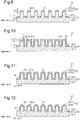
- the metal layer 31 includes a base surface metal layer 61 located on base surface 41a and a top surface metal layer 62 located on the top surface 42a, the thickness of the base surface metal layer 61 is a base surface thickness T1, and the thickness of the top surface metal layer 62 is a top surface thickness T2.
- the metal layer 31 is formed by the above-described physical vapor deposition method, for example, a vacuum vapor deposition method, particles constituting the metal layer 31 easily reach the top surface 42a of each protrusion 42 in comparison with the base surface 41a. For this reason, typically, the top surface thickness T2 is equal to or greater than the base surface thickness T1.
- the top surface metal layer 62 includes a flat portion 62a located along the shape of the top surface 42a and a curved peripheral surface portion 62b, which is provided around the flat portion 62a and curved to protrude from the flat portion 62a toward the outside. That is, the curved peripheral surface portion 62b has a curved surface shape which protrudes toward the outside of the flat portion 62a.
- a radius of curvature of the curved peripheral surface portion 62b is preferably (T2/2) or more and (4 x T2) or less, more preferably (T2/2) or more and (2 x T2) or less.
- a part between the protrusions 42 adjacent to each other in the Y direction in the base surface metal layer 61 is configured by a curved surface in which a substantial center between the two protrusions 42 protrudes in the direction away from the base surface 41a.
- a part between the protrusions 42 adjacent to each other in the X direction in the base surface metal layer 61 is configured by a curved surface in which a substantial center between the two protrusions 42 protrudes in the direction away from the base surface 41a.
- the radius of curvature in these portions is preferably (T1/2) or more and (4 x T1) or less, more preferably (T1/2) or more and (2 x T1) or less.
- the parts not between the two protrusions 42 in both of the X and Y directions in the base surface metal layer 61 are configured with substantially flat surfaces because the flying angle of the particles for forming the metal layer 31 which reach the base surface 41a is not limited.
- each of the base surface metal layer 61 and the top surface metal layer 62 has a curved surface, it is possible to obtain the advantages listed below.
- the side surface thickness T3 may be equal to or greater than each of the top surface thickness T2 and the base surface thickness T1.
- the top surface metal layer 62 may have the configuration illustrated in Fig. 8
- the base surface metal layer 61 may have the configuration illustrated in Fig. 8
- the side surface thickness T3 of the side surface metal layer 63 may be, for example, configured to become less as the distance to the top surface 42a decreases and to become greater as the distance to the base surface 41a decreases.
- the thickness of the side surface metal layer 63 may be substantially the same over the entire side surface metal layer 63.
- the top surface metal layer 62 may have the configuration illustrated in Fig. 9
- the base surface metal layer 61 may have the configuration illustrated in Fig. 9
- the side surface thickness T3 of the side surface metal layer 63 may be, for example, configured to become less as the distance to the top surface 42a decreases and to become greater as the distance to the base surface 41a decreases.
- the thickness of the side surface metal layer 63 may be substantially the same over the entire side surface metal layer 63.
- the protrusions 42 included in the dielectric layer 32 do not necessarily need to be arranged in a tetragonal lattice shape.
- the protrusions 42 may be arranged in a hexagonal lattice shape.
- distances between one protrusion 42 and six protrusions 42 located around the one protrusion 42 are equal to each other. That is, all of the protrusions 42 are arranged in the state that the adjacent protrusions 42 are separated from each other by a period P as an equal interval.
- the protrusions 42 included in the dielectric layer 32 are not limited to the tetragonal lattice shape or the hexagonal lattice shape, the protrusions may be arranged in a trigonal lattice shape.
- the first display elements 22 included in the micro-display part 13 may include two or more plasmon structures having different colors in transmitted light, and the second display element 23 may include two or more plasmon structures having different colors in transmitted light.
- the first display element 22 includes two first portions 71 and two second portions 72, and each first portion 71 and each second portion 72 are configured with plasmon structures transmitting light having different colors.
- the first portions 71 and the second portions 72 are, for example, arranged alternately in the column direction C and arranged alternately in the row direction R.
- the light transmitted by the first display element 22 has a mixed color of the color of the light transmitted by each of the first portions 71 and the color of the light transmitted by each of the second portions 72. For this reason, it is possible to increase the number of colors which can be displayed by the micro-display part 13.
- the first portions 71 and the second portions 72 do not necessarily need to be arranged alternately in the column direction C or the row direction R, and the number of first portions 71 included in the first display element 22 may be different from the number of the second portions 72.
- the first display elements 22 if the first portions 71 and the second portions 72 are configured to be arranged alternately in each of the column direction C and the row direction R and the number of first portions 71 included in the first display element 22 is configured to be equal to the number of second portions 72, deviation in color of the first display elements 22 can be eliminated. For this reason, the first display elements 22 can be easily recognized as the display element 21 displaying one color.
- the second display element 23 includes a plurality of first portions 73 and a plurality of second portions 74, and the first portions 73 and the second portions 74 transmit light having different colors.
- the first portion 73 included in the second display element 23 may include a plasmon structure transmitting the light having the same color as that of any one of the first portion 71 or the second portion 72 included in the first display element 22.
- the second portion 74 included in the second display element 23 may include a plasmon structure transmitting the light having the same color as that of any one of the first portion 71 and the second portion 72 included in the first display element 22.
- the first portions 73 and the second portions 74 are, for example, arranged alternately in the column direction C and arranged alternately in the row direction R.
- the first portions 73 and the second portions 74 do not necessarily need to be arranged alternately in the column direction C or the row direction R.
- each of the first display elements 22 and each of the second display elements 23 transmit light having a mixed color
- the first display elements 22 include the first portions 71 or the second portions 72 as a set of the plasmon structures
- the plasmon structures transmitting light having different colors be located in a mixed manner inside the first display elements 22.
- Such a configuration is also preferred in the second display element 23. Therefore, deviation in color displayed by each display element can be further restrained.
- each display element 21 includes a plurality of plasmon structures having transmitted light having different colors, one display element 21 can transmit light having a mixed color of multiple colors. Therefore, it is possible to increase the number of colors which can be displayed by the micro-display part 13.
- the size of the display part 12 does not necessarily need to be such a size that the display size of the second information displayed by the display part 12 can be visually recognized. If the display part 12 has a size capable of including at least one micro-display part 13, the display part 12 may have a size to an extent that the display part 12 can be observed by an optical microscope.
- the display element 21 may have a configuration of transmitting white light.
- the display element 21 for example, by configuring the periods P of a plurality of protrusions 42 to be irregular or configuring the heights of the protrusions 42 to be irregular, the states of the surface plasmons formed in minimum units of the plasmon structures become different from each other, so that the display element 21 transmits white light.
- the surface plasmons having different states can be easily excited inside the display element 21. For this reason, the light transmitted by the display element 21 becomes mixed light of a plurality of light beams having different wavelengths.
- the light irradiated in the irradiation process does not necessarily need to be white light. Even in such a configuration, if the irradiation light includes light of which the color can be changed by the plasmon structure included in the micro-display part 13, it is possible to obtain the advantage in accordance with the above-described advantage (1).
- the number of display elements 21 arranged in the row direction R and the number of display elements 21 arranged in the column direction C may be less than 10 or may be more than 100. Even in such a configuration, the size of one micro-display part 13 may be such a size that the micro-display part 13 is included in the display part 12 as a part of the display part 12. As long as the micro-display part 13 includes the plasmon structure, it is possible to obtain the advantage in accordance with the above-described advantage (1).
- the length L1 of one side of the display element 21 may be less than 200 nm or may be greater than 3000 nm. Even in such a configuration, the size of the micro-display part 13 may be a size that the micro-display part 13 is included in the display part 12 as a part of the display part 12.
- All of the display elements 21 constituting the micro-display part 13 may transmit light having the same color. Even in such a configuration, as long as each display element 21 includes the plasmon structure, it is possible to obtain the advantage in accordance with the above-described advantage (1).
- the period P of the formation of the protrusions 42 may be less than 100 nm or may be greater than 600 nm as long as surface plasmons are excited in the interface 33 between the metal layer 31 and the dielectric layer 32 to change the irradiation light to transmitted light having a color different from that of the irradiation light.
- the real part of the complex dielectric constant in a visible light range may be 0 or more. Even in such a configuration, if the micro-display part 13 includes the plasmon structure including the interface 33 between the metal layer 31 and the dielectric layer 32, the plasmon structure can be embodied as a structure transmitting light having any one of wavelengths included in the visible light range.
- the thickness of the metal layer 31 may be less than 20 nm or may be greater than 100 nm. Even in such a configuration, if the micro-display part 13 includes the plasmon structure including the interface 33 between the metal layer 31 and the dielectric layer 32, the irradiation light can be changed to the transmitted light having a color different from that of the irradiation light by the surface plasmons excited in the plasmon structure.
- the distance between the base surface 41a and the imaginary plane 42b may be less than 30 nm or may be greater than 500 nm. Even in such a configuration, if the micro-display part 13 includes the plasmon structure including the interface 33 between the metal layer 31 and the dielectric layer 32, the irradiation light can be changed to the transmitted light having a color different from that of the irradiation light by the surface plasmons excited by the plasmon structure.
- the base surface 41a of the base body 41 and the imaginary plane 42b including the top surface 42a of each of the protrusions 42 do not necessarily need to be substantially parallel to each other, but for example, the base surface 41a and the imaginary plane 42b may be crossed at a predetermined angle. Even in such a configuration, if the micro-display part 13 includes the plasmon structure including the interface 33 between the metal layer 31 and the dielectric layer 32, the irradiation light can be changed to the transmitted light having a color different from that of the irradiation light by the surface plasmons excited by the plasmon structure.
- the display body 10 may include a print layer as described hereinafter with reference to Figs. 16 to 19 .
- the display body 10 includes a print layer 81, and the print layer 81 is configured with a plurality of print portions 82 having a wavy line shape.
- the print portions 82 are arranged on the substrate 11 to be spaced at a predetermined interval in one direction.
- each print portion 82 may be arranged at a position which overlaps with the display part 12 and does not overlap with the micro-display part 13.
- the print layer 81 forms an example of a colored figure pattern as a pattern formed with a plurality of wavy line shapes.
- the print layer 81 may form a colored figure pattern formed with a plurality of circular arc shapes or a colored figure pattern formed with a plurality of circular shapes.
- the print layer 81 may form a colored figure pattern formed by combining two or more of the shapes of the wavy line shape, the circular arc shape, and the circular shape.
- the print layer 81 may form a pattern formed with geometric shapes other than the wavy line shape, the circular arc shape, and the circular shape. That is, the image as information displayed by the print layer 81 may be a predetermined design pattern.
- a print layer 91 included in the display body 10 does not necessarily need to be in the form of the above-described predetermined design pattern, but it may form individual information such as a card number and a lot number as information including at least one of characters and numerals. That is, the image as information displayed by the print layer 91 may include at least one of predetermined characters and numerals.
- the print layer 91 is configured with a plurality of print portions 92, and the print portions 92 are arranged in the substrate 11 in a predetermined direction.
- Each print portion 92 displays, for example, one numeral, and the print portions 92 display a numeral "1", a numeral "2", and a numeral "3" in the order from the print portion 92 located in the shortest distance from the one end of the substrate 11.
- each print portion 92 overlaps with the display part 12. As viewed from the direction facing the display part 12, at least a part of the print portion 92 overlapping with the display part 12 overlaps with at least one of the micro-display parts 13. Furthermore, as viewed from the direction facing the display part 12, each print portion 92 may be arranged at a position which overlaps with the display part 12 and does not overlap with the micro-display part 13.
- the image as information displayed by the print layers 81 and 91 is not limited to the aforementioned design patterns, characters, and numerals, but the image may be figures or symbols or may be a combination of at least two of design patterns, characters, numerals, figures, and symbols.
- a cross-sectional structure of the display body 10 will now be described with reference to Figs. 18 and 19 .
- the display body 10 described with reference to Fig. 16 and the display body 10 described with reference to Fig. 17 are different from each other in terms of the image displayed by the print layer, the part where the print layer is arranged in the display body 10 is common to the two display bodies 10.
- the cross-sectional structure of the display body 10 described with reference to Fig. 16 is described, and the description of the cross-sectional structure of the display body 10 described with reference to Fig. 17 is omitted.
- the substrate 11 includes the dielectric layer 32 included in the micro-display part 13, and among the surfaces of the substrate 11, a surface including the base surface 41a of the dielectric layer 32 is a front surface 11a and a surface which is opposite to the front surface 11a in the substrate 11 is a back surface 11b.
- the display part 12 formed with the metal layer may be arranged on the front surface 11a of the substrate 11, and the display part 12 may be formed with a metal layer common to the metal layer 31 included in the micro-display part 13 or may be formed with a metal layer different from the metal layer 31 included in the micro-display part 13.
- the print portions 82 constituting the print layer 81 are formed on the back surface 11b of the substrate 11.
- the print portions 82 are portions formed, for example, by ink or the like containing predetermined dye or pigment and portions formed by using various printing methods, for example, a gravure printing method, an offset printing method, a screen printing method, and the like.
- the print layer 81 may be formed in portions other than the back surface 11b of the substrate 11. That is, as illustrated in Fig. 19 , a transparent plastic layer 101 covering the display part 12 and the micro-display part 13 is formed on the front surface 11a of the substrate 11.
- the transparent plastic layer 101 is a layer formed by a plastic capable of transmitting light.
- a surface which is opposite to the surface being in contact with the front surface 11a of the substrate 11 is a front surface 101a, and the print portions 82 are formed on the front surface 101a.
- the transparent plastic layer 101 may be a layer having adhesiveness for attaching the display body 10 to a product such as an object-to-be-authenticated, and the layer having adhesiveness may be formed on the front surface 101a of the transparent plastic layer 101 or the back surface 11b of the substrate 11 separately from the transparent plastic layer 101.
- the print layers 81 may be formed on both of the front surface 101a of the transparent plastic layer 101 and the back surface 11b of the substrate 11.
- the display body 10 includes the above-described print layer 81 and the print layer 81 is arranged on the back surface 11b of the substrate 11, when the display body 10 is visually recognized from the side of the back surface 11b of the substrate 11, a part of the display part 12, that is, a part of the second information displayed by the display part 12 can be concealed from the observer by the print layer 81.
- the display body 10 in the configuration in which the print layer 81 is arranged on the front surface 101a of the transparent plastic layer 101, when the display body 10 is visually recognized from the side of the front surface 101a of the transparent plastic layer 101, a part of the display part 12, that is, a part of the second information displayed by the display part 12 can be concealed from the observer by the print layer 81.
- the observer faces the display body 10, that is, as viewed from the direction normal to the display part 12, the information displayed by the print layer 81 is visually recognized.
- the observer observes the display body 10 in a slanted direction, as viewed from the direction facing the display part 12, a part of the display part 12 overlapping with the print layer 81 is visually recognized.
- the display body 10 including the print layer 81 by changing the angle at which the observer observes the display body 10, the information displayed by the print layer 81 and the part of the second information concealed by the print layer 81 can be individually observed. Since the print layer 81 is a layer formed by ink as described above and the display part 12 is a layer formed with the metal layer, the print layer 81 has optical effects different from those of the display part 12, so that the second information can be easily recognized.
- the print layer 81 and the display part 12 may be configured to be located to be separated from each other, that is, the print layer 81 may be configured not to conceal the display part 12 and the second information displayed by the display part 12.
- the information displayed by the print layer 81 and the second information displayed by the display part 12 can be individually observed. Since the print layer 81 has optical effects different from those of the display part 12, the second information can be easily recognized.
- the print layer 81 conceals at least one of the micro-display parts 13, that is, at least one piece of first information. According to such a configuration, the region where the first information is displayed can be restricted by the print layer 81, so that the position where the first information is arranged can be inconspicuous.
- the print layer 81 and the display part 12 can be configured to be located to be separated from each other, that is, the print layer 81 can be configured not to conceal the first information displayed by the micro-display part 13.
- the observer of the display body 10 when the observer of the display body 10 observes the second information, the observer focuses attention on the second information and the information displayed by the print layer 81. It is thus difficult to notice that information other than the second information and the information displayed by the print layer 81 can be displayed by the display body 10. Therefore, in the display body 10, it is possible to make it more difficult to notice the first information.
- the first information is observed, in the display body 10, since the light amount of the transmitted light in the part other than the micro-display parts 13 can be reduced by the print layer 81, the contrast between the first information and the periphery of the first information is increased, so that the first information can be more easily recognized.
- This advantage can be obtained from any one of the configuration in which the print layer 81 is formed on the back surface 11b of the substrate 11 and the configuration in which the print layer 81 is formed on the front surface 101a of the transparent plastic layer 101. This advantage can be obtained from both the case in which the display body 10 is visually recognized from the side of the front surface 11a of the substrate 11 and the case in which the display body 10 is visually recognized from the back surface 11b.
- the same advantages as those obtained by the print layer 81 can also be obtained by the display body 10 including a print layer 91 illustrated in Fig. 19 .
- an object-to-be-authenticated 50 attached with the display body 10 may have a print layer 51.
- the print layer 51 is configured to include a plurality of print portions 52, and as viewed from the direction facing the display part 12, each of the print portions 52 is connected to one of the print portions 82 formed in the display body 10. That is, the print layer 81 included in the display body 10 and the print layer 51 included in the object-to-be-authenticated 50 display one colored figure pattern.
Claims (15)
- Anzeigekörper (10), mit:einem ersten Anzeigeteil (13), der erste Informationen anzeigt; undeinem zweiten Anzeigeteil (12), der zweite Informationen mit einer Anzeigegröße anzeigt, die größer als die der ersten Informationen ist, wobeider zweite Anzeigeteil (12) den gesamten ersten Anzeigeteil (13) als einen Teil des zweiten Anzeigeteils enthält (12),der erste Anzeigeteil (13) eine Plasmonenstruktur enthält, unddie Plasmonenstruktur dazu eingerichtet ist, umeine Grenzfläche (33) zwischen einer Metallschicht (31) und einer dielektrischen Schicht (32), die Licht durchlässt, zu enthalten,Oberflächenplasmonen in der Grenzfläche (33) anzuregen, um ein Bestrahlungslicht, mit dem die Grenzfläche (33) bestrahlt wird, in ein Durchlicht mit einer von der des Bestrahlungslichts unterschiedlichen Farbe zu ändern,die ersten Informationen mit dem Durchlicht anzuzeigen, wobeidie ersten Informationen eine Vielzahl von Informationselementen enthalten,der erste Anzeigeteil (13) eine Vielzahl von Anzeigeelementen (21) enthält, undjedes Anzeigeelement (21) einem der Informationselemente entspricht,die Vielzahl von Anzeigeelementen (21) ein erstes Anzeigeelement (22) enthält,das erste Anzeigeelement (22) einen ersten Abschnitt (71) und einen zweiten Abschnitt (72) enthält,dadurch gekennzeichnet, dassder erste Abschnitt (71) und der zweite Abschnitt (72) mit Plasmonenstrukturen, die Licht verschiedener Farben durchlassen, derart eingerichtet sind, dassdas von dem ersten Anzeigeelement (22) durchgelassene Licht eine Mischfarbe aus der Farbe des von dem ersten Abschnitt (71) durchgelassenen Lichts und der Farbe des von dem zweiten Abschnitt (72) durchgelassenen Lichts aufweist.
- Anzeigekörper (10) nach Anspruch 1, wobei
die Vielzahl von Informationselementen ein erstes Informationselement, das eine erste Farbe darstellt, und ein zweites Informationselement, das eine zweite Farbe darstellt, umfasst. - Anzeigekörper (10) nach Anspruch 1 oder 2, wobei mindestens eines der Anzeigeelemente (21) eine Vielzahl der Plasmonenstrukturen enthält, die das Bestrahlungslicht in das Durchlicht mit unterschiedlichen Farben ändert.
- Anzeigekörper (10) nach einem der Ansprüche 1 bis 3, wobei
die dielektrische Schicht (32) eine Basisoberfläche (41a) und eine Vielzahl von Vorsprüngen (42), die aus der Basisoberfläche (41a) herausragen (41a), umfasst,
wobei die Basisoberfläche (41a) und eine imaginäre Ebene (42b) einschließlich oberen Oberflächen (42a) einer Vielzahl der Vorsprünge (42) im Wesentlichen parallel zueinander sind, und
die Metallschicht (31) mindestens einen Teil der dielektrischen Schicht (32) bedeckt. - Anzeigekörper (10) nach Anspruch 4, wobei in der dielektrischen Schicht (32) ein Abstand zwischen der Basisoberfläche (41a) und der imaginären Ebene (42b) 30 nm oder mehr und 500 nm oder weniger beträgt.
- Anzeigekörper (10) nach Anspruch 4 oder 5, wobei
eine Dicke (T) der Metallschicht (31) 20 nm oder mehr und 100 nm oder weniger beträgt, und
in einem Material zum Bilden der Metallschicht (31) ein Realteil einer komplexen Dielektrizitätskonstante in einem sichtbaren Lichtbereich einen negativen Wert aufweist. - Anzeigekörper (10) nach einem der Ansprüche 4 bis 6, wobei
in der Metallschicht (31) ein Teil, der sich auf der oberen Oberfläche (42a) befindet, einen flachen Abschnitt (62a), der sich entlang der oberen Oberfläche (42a) erstreckt, und eine Umfangsoberfläche (62b) mit einer gekrümmten Form, die in einem Umfang des flachen Abschnitts (62a) bereitgestellt ist und in Richtung einer Außenseite des flachen Abschnitts (62a) vorsteht, enthält, und
in der Metallschicht (31) ein Teil, der auf der Basisoberfläche (41a) angeordnet ist, eine konvexe Form aufweist, die am stärksten in einem wesentlichen Zentrum eines Gebiets zwischen den nebeneinander liegenden Vorsprüngen (42) hervorsteht. - Anzeigekörper (10) nach einem der Ansprüche 4 bis 7, wobei
jeder der Vorsprünge (42) eine Seitenoberfläche (42c) aufweist, die die obere Oberfläche (42a) und die Basisoberfläche (41a) verbindet, und
die Metallschicht (31) die Basisoberfläche (41a) und die obere Oberfläche (42a) von jedem der Vorsprünge (42) bedeckt und mindestens einen Teil der Seitenoberfläche (42c) bedeckt. - Anzeigekörper (10) nach Anspruch 8, wobei in der Metallschicht (31) eine Dicke eines die Seitenoberfläche (42c) bedeckenden Teils geringer als eine Dicke eines die obere Oberfläche (42a) bedeckenden Teils und als eine Dicke eines die Basisoberfläche (41a) bedeckenden Teils ist.
- Anzeigekörper (10) nach einem der Ansprüche 4 bis 9, wobei
die Vielzahl von Vorsprüngen (42) in der Basisoberfläche (41a) in einem Zustand einer trigonalen Gitterform, einer tetragonalen Gitterform oder einer hexagonalen Gitterform angeordnet ist, und
von einer Ebene aus gesehen, die der Basisoberfläche (41a) zugewandt ist, ein Abstand zwischen Zentren der Vorsprünge (42) in den nebeneinander liegenden Vorsprüngen (42) 100 nm oder mehr und 600 nm oder weniger beträgt. - Anzeigekörper (10) nach einem der Ansprüche 4 bis 9, wobei die Vielzahl von Vorsprüngen (42) unregelmäßig auf der Basisoberfläche (41a) angeordnet ist.
- Anzeigekörper (10) nach Anspruch 4, wobei
jedes der Vielzahl von Anzeigeelementen (21) mit einem mindestens einen der Vorsprünge (42) enthaltenen Teil der dielektrischen Schicht (32) eingerichtet ist, und
sich in mindestens einem Teil der Vielzahl von Anzeigeelementen (21) mindestens ein Zwischenzentrumsabstand zwischen den Vorsprüngen (42), gesehen von einer der Basisoberfläche (41a) zugewandten Ebene, ein Abstand zwischen der Basisoberfläche (41a) und der imaginären Ebene (42b), ein Anordnungszustand der Vorsprünge (42), eine Dicke (T) der Metallschicht (31) oder ein Material zum Bilden der Metallschicht (31) zwischen den Anzeigeelementen (21) unterscheidet. - Anzeigekörper (10) nach Anspruch 12, wobei
jedes der Anzeigeelemente (21) ein polygonales Gebiet definiert und
eine Länge einer Seite des polygonalen Gebiets 200 nm oder mehr und 3000 nm oder weniger beträgt. - Anzeigekörper (10) nach Anspruch 12 oder 13, wobei
die Vielzahl von Anzeigeelementen (21) in einer Matrixform angeordnet ist, und
die Anzahl der Anzeigeelemente (21), die in einer Zeilenrichtung (R) und einer Spaltenrichtung (C) senkrecht zu der Zeilenrichtung (R) angeordnet sind, jeweils 10 oder mehr und 100 oder weniger beträgt. - Verfahren zum Beobachten eines Anzeigekörpers (10), wobei der Anzeigekörper (10) umfasst:einen ersten Anzeigeteil (13), der erste Informationen anzeigt; undeinen zweiten Anzeigeteil (12), der zweite Informationen mit einer Anzeigegröße anzeigt, die größer als die der ersten Informationen ist, wobeider zweite Anzeigeteil (12) den gesamten ersten Anzeigeteil (13) als einen Teil des zweiten Anzeigeteils enthält (12),
der erste Anzeigeteil (13) eine Plasmonenstruktur enthält, und
die Plasmonenstruktur dazu eingerichtet ist, umeine Grenzfläche (33) zwischen einer Metallschicht (31) und einer dielektrischen Schicht (32), die Licht durchlässt, zu enthalten,Oberflächenplasmonen in der Grenzfläche (33) anzuregen, um ein Bestrahlungslicht, mit dem die Grenzfläche (33) bestrahlt wird, in ein Durchlicht mit einer von der des Bestrahlungslichts unterschiedlichen Farbe zu ändern, unddie ersten Informationen mit dem Durchlicht anzuzeigen, wobeidie ersten Informationen eine Vielzahl von Informationselementen enthalten,
der erste Anzeigeteil (13) eine Vielzahl von Anzeigeelementen (21) enthält, und
jedes Anzeigeelement (21) einem der Informationselemente entspricht,
die Vielzahl von Anzeigeelementen (21) ein erstes Anzeigeelement (22) enthalten,
das erste Anzeigeelement (22) einen ersten Abschnitt (71) und einen zweiten Abschnitt (72) enthält,
dadurch gekennzeichnet, dass
der erste Abschnitt (71) und der zweite Abschnitt (72) mit Plasmonenstrukturen, die Licht verschiedener Farben durchlassen, derart eingerichtet sind, dass
das von dem ersten Anzeigeelement (22) durchgelassene Licht eine Mischfarbe aus der Farbe des von dem ersten Abschnitt (71) durchgelassenen Lichts und der Farbe des von dem zweiten Abschnitt (72) durchgelassenen Lichts aufweist,
wobei das Verfahren umfasst:Bestrahlen der Grenzfläche (33) des Anzeigekörpers (10) mit dem Bestrahlungslicht; undBeobachten des mit dem Bestrahlungslicht bestrahlten Anzeigekörpers (10) in vergrößernder Weise.
Applications Claiming Priority (3)
| Application Number | Priority Date | Filing Date | Title |
|---|---|---|---|
| JP2014065630 | 2014-03-27 | ||
| PCT/JP2015/059688 WO2015147283A1 (ja) | 2014-03-27 | 2015-03-27 | 表示体、および、表示体の観察方法 |
| EP15770172.3A EP3124283B1 (de) | 2014-03-27 | 2015-03-27 | Anzeigekörper und beobachtungsverfahren für den anzeigekörper |
Related Parent Applications (2)
| Application Number | Title | Priority Date | Filing Date |
|---|---|---|---|
| EP15770172.3A Division-Into EP3124283B1 (de) | 2014-03-27 | 2015-03-27 | Anzeigekörper und beobachtungsverfahren für den anzeigekörper |
| EP15770172.3A Division EP3124283B1 (de) | 2014-03-27 | 2015-03-27 | Anzeigekörper und beobachtungsverfahren für den anzeigekörper |
Publications (2)
| Publication Number | Publication Date |
|---|---|
| EP3450196A1 EP3450196A1 (de) | 2019-03-06 |
| EP3450196B1 true EP3450196B1 (de) | 2020-06-10 |
Family
ID=54195787
Family Applications (2)
| Application Number | Title | Priority Date | Filing Date |
|---|---|---|---|
| EP15770172.3A Revoked EP3124283B1 (de) | 2014-03-27 | 2015-03-27 | Anzeigekörper und beobachtungsverfahren für den anzeigekörper |
| EP18202229.3A Active EP3450196B1 (de) | 2014-03-27 | 2015-03-27 | Anzeigekörper und beobachtungsverfahren für den anzeigekörper |
Family Applications Before (1)
| Application Number | Title | Priority Date | Filing Date |
|---|---|---|---|
| EP15770172.3A Revoked EP3124283B1 (de) | 2014-03-27 | 2015-03-27 | Anzeigekörper und beobachtungsverfahren für den anzeigekörper |
Country Status (7)
| Country | Link |
|---|---|
| US (1) | US10186175B2 (de) |
| EP (2) | EP3124283B1 (de) |
| JP (1) | JP6645422B2 (de) |
| CN (1) | CN106132722B (de) |
| AU (2) | AU2015234717B2 (de) |
| CA (1) | CA2943501C (de) |
| WO (1) | WO2015147283A1 (de) |
Families Citing this family (17)
| Publication number | Priority date | Publication date | Assignee | Title |
|---|---|---|---|---|
| WO2015147283A1 (ja) | 2014-03-27 | 2015-10-01 | 凸版印刷株式会社 | 表示体、および、表示体の観察方法 |
| JP6627481B2 (ja) * | 2015-12-15 | 2020-01-08 | 凸版印刷株式会社 | 表示体、および、表示体の観察方法 |
| JP2017215580A (ja) * | 2016-05-27 | 2017-12-07 | 大日本印刷株式会社 | 表示体、印刷物および情報記録媒体 |
| CN109328314A (zh) * | 2016-06-24 | 2019-02-12 | 凸版印刷株式会社 | 光学装置、显示体、带显示体的装置、滤光镜、以及光学装置的制造方法 |
| JP7024221B2 (ja) * | 2016-06-24 | 2022-02-24 | 凸版印刷株式会社 | 表示体、表示体付きデバイス、および、表示体の製造方法 |
| JP6790498B2 (ja) * | 2016-06-24 | 2020-11-25 | 凸版印刷株式会社 | 表示体 |
| JP6805668B2 (ja) * | 2016-09-15 | 2020-12-23 | 凸版印刷株式会社 | 表示体、表示体付きデバイス、および、表示体の製造方法 |
| JP7009789B2 (ja) * | 2017-06-13 | 2022-01-26 | 凸版印刷株式会社 | 光学素子および個人認証媒体 |
| WO2019039572A1 (ja) * | 2017-08-23 | 2019-02-28 | 凸版印刷株式会社 | 表示体、偽造防止スレッド用紙、および偽造防止媒体 |
| JP2019113688A (ja) * | 2017-12-22 | 2019-07-11 | 凸版印刷株式会社 | 表示体 |
| WO2019111826A1 (ja) * | 2017-12-04 | 2019-06-13 | 凸版印刷株式会社 | 表示体、表示体付きデバイス、および、表示体の製造方法 |
| JP2019117289A (ja) * | 2017-12-27 | 2019-07-18 | 凸版印刷株式会社 | 表示体 |
| JP7139595B2 (ja) * | 2017-12-04 | 2022-09-21 | 凸版印刷株式会社 | 表示体、表示体付きデバイス、および、表示体の製造方法 |
| DE102017130589A1 (de) * | 2017-12-19 | 2019-06-19 | Giesecke+Devrient Currency Technology Gmbh | Sicherheitselement mit zweidimensionaler Nanostruktur und Herstellverfahren für dieses Sicherheitselement |
| CN110857003B (zh) * | 2018-08-23 | 2020-12-25 | 中钞特种防伪科技有限公司 | 光学防伪元件及其设计方法、防伪产品 |
| JP7225612B2 (ja) * | 2018-08-31 | 2023-02-21 | 凸版印刷株式会社 | 表示体 |
| GB2578773B (en) * | 2018-11-08 | 2022-03-30 | De La Rue Int Ltd | Methods of manufacturing security device components |
Citations (9)
| Publication number | Priority date | Publication date | Assignee | Title |
|---|---|---|---|---|
| JP2009046742A (ja) | 2007-08-22 | 2009-03-05 | Toppan Printing Co Ltd | メタルワイヤーパタンの製造方法、バックライトシステム及びそれらを用いた液晶ディスプレイ |
| WO2009083151A1 (de) | 2007-12-21 | 2009-07-09 | Giesecke & Devrient Gmbh | Sicherheitselement |
| DE102009012300A1 (de) | 2009-03-11 | 2010-09-16 | Giesecke & Devrient Gmbh | Sicherheitselement mit mehrfarbigem Bild |
| WO2012156049A1 (de) | 2011-05-16 | 2012-11-22 | Giesecke & Devrient Gmbh | Zweidimensional periodisches, farbfilterndes gitter |
| JP2013174683A (ja) | 2012-02-24 | 2013-09-05 | Toppan Printing Co Ltd | 表示体および表示体の観察方法 |
| WO2014001283A1 (de) | 2012-06-26 | 2014-01-03 | Ovd Kinegram Ag | Dekorelement sowie sicherheitsdokument mit einem dekorelement |
| US20140028012A1 (en) | 2011-04-08 | 2014-01-30 | Universite Jean Monnet | Optical safety component having a transmissive effect, manufacture of such a component, and secure document provided with such a component |
| WO2014023415A1 (de) | 2012-08-10 | 2014-02-13 | Giesecke & Devrient Gmbh | Sicherheitselement mit farbeffekterzeugender struktur |
| EP3124283B1 (de) | 2014-03-27 | 2018-12-12 | Toppan Printing Co., Ltd. | Anzeigekörper und beobachtungsverfahren für den anzeigekörper |
Family Cites Families (23)
| Publication number | Priority date | Publication date | Assignee | Title |
|---|---|---|---|---|
| JP3534316B2 (ja) * | 2002-04-17 | 2004-06-07 | 独立行政法人 国立印刷局 | 真偽判別可能な凹凸模様入り積層体 |
| EP1862827B2 (de) * | 2006-05-31 | 2012-05-30 | CSEM Centre Suisse d'Electronique et de Microtechnique SA - Recherche et Développement | Nanostrukturierter Diffraktionsfilter nullter Ordnung |
| JP4940858B2 (ja) | 2006-09-26 | 2012-05-30 | 凸版印刷株式会社 | ディスプレイ |
| JP5157115B2 (ja) * | 2006-09-28 | 2013-03-06 | 凸版印刷株式会社 | 回折格子から成る表示体およびそれを応用した印刷物 |
| CA2613830A1 (en) * | 2006-12-15 | 2008-06-15 | Alberto Argoitia | An article with micro indicia security enhancement |
| EP2100747B1 (de) * | 2008-03-10 | 2015-02-25 | Maurer Electronics Gmbh | Verfahren zum Aufbringen eines Bildes mit eingebetteter Zusatzinformation auf einen Datenträger |
| JP5597940B2 (ja) * | 2009-06-02 | 2014-10-01 | 凸版印刷株式会社 | 表示体、粘着ラベル、転写箔及びラベル付き物品 |
| JP2011194837A (ja) * | 2010-03-23 | 2011-10-06 | Toppan Printing Co Ltd | 画像表示体及びラベル付き物品 |
| CN104090319B (zh) | 2009-08-13 | 2017-06-20 | 凸版印刷株式会社 | 图像显示体及带标签的物品 |
| US8696940B2 (en) * | 2009-10-30 | 2014-04-15 | United States Of America As Represented By The Administrator Of The National Aeronautics And Space Administration | Negative dielectric constant material based on ion conducting materials |
| FR2982038B1 (fr) * | 2011-10-28 | 2013-11-15 | Hologram Ind | Composant optique de securite a effet reflectif, fabrication d'un tel composant et document securise equipe d'un tel composant |
| JP6225408B2 (ja) * | 2011-11-01 | 2017-11-08 | 凸版印刷株式会社 | 表示体及びその真偽判定方法 |
| JP5938963B2 (ja) * | 2012-03-16 | 2016-06-22 | 凸版印刷株式会社 | 表示体及びラベル付き物品 |
| JP5935429B2 (ja) * | 2012-03-21 | 2016-06-15 | 凸版印刷株式会社 | 偽造防止媒体の識別方法 |
| JP2013218595A (ja) * | 2012-04-11 | 2013-10-24 | Toppan Printing Co Ltd | 表示体およびその真贋判定方法 |
| US9335027B2 (en) * | 2013-01-02 | 2016-05-10 | Massachusetts Institute Of Technology | Methods and apparatus for transparent display using scattering nanoparticles |
| JP6237759B2 (ja) * | 2013-02-21 | 2017-11-29 | 凸版印刷株式会社 | 表示体およびラベル付き物品 |
| KR101449272B1 (ko) * | 2013-04-22 | 2014-10-08 | 한국기계연구원 | 전사기반의 임프린팅 공정을 이용한 함몰패턴 제작방법 |
| US20160107472A1 (en) * | 2013-06-26 | 2016-04-21 | Fábrica Nacional De Moneda Y Timbre - Real Casa De La Moneda | Method of providing a security document with a security feature, and security document |
| US9460665B2 (en) * | 2013-08-11 | 2016-10-04 | NanoMedia Solutions Inc. | Nano-media information carrier based on pixelated nano-structures combined with an intensity control layer |
| US10414194B2 (en) * | 2013-11-08 | 2019-09-17 | Bank Of Canada | Optically variable devices, their production and use |
| FR3017231B1 (fr) * | 2014-01-31 | 2020-07-24 | Hologram Ind | Composant optique de securite a effet plasmonique, fabrication d'un tel composant et document securise equipe d'un tel composant |
| WO2015183243A1 (en) * | 2014-05-27 | 2015-12-03 | Rolith, Inc. | Anti-counterfeiting features and methods of fabrication and detection |
-
2015
- 2015-03-27 WO PCT/JP2015/059688 patent/WO2015147283A1/ja active Application Filing
- 2015-03-27 AU AU2015234717A patent/AU2015234717B2/en active Active
- 2015-03-27 CA CA2943501A patent/CA2943501C/en active Active
- 2015-03-27 EP EP15770172.3A patent/EP3124283B1/de not_active Revoked
- 2015-03-27 EP EP18202229.3A patent/EP3450196B1/de active Active
- 2015-03-27 CN CN201580015533.XA patent/CN106132722B/zh active Active
- 2015-03-27 JP JP2016510559A patent/JP6645422B2/ja active Active
-
2016
- 2016-09-22 US US15/272,780 patent/US10186175B2/en active Active
-
2017
- 2017-12-14 AU AU2017276267A patent/AU2017276267B2/en active Active
Patent Citations (9)
| Publication number | Priority date | Publication date | Assignee | Title |
|---|---|---|---|---|
| JP2009046742A (ja) | 2007-08-22 | 2009-03-05 | Toppan Printing Co Ltd | メタルワイヤーパタンの製造方法、バックライトシステム及びそれらを用いた液晶ディスプレイ |
| WO2009083151A1 (de) | 2007-12-21 | 2009-07-09 | Giesecke & Devrient Gmbh | Sicherheitselement |
| DE102009012300A1 (de) | 2009-03-11 | 2010-09-16 | Giesecke & Devrient Gmbh | Sicherheitselement mit mehrfarbigem Bild |
| US20140028012A1 (en) | 2011-04-08 | 2014-01-30 | Universite Jean Monnet | Optical safety component having a transmissive effect, manufacture of such a component, and secure document provided with such a component |
| WO2012156049A1 (de) | 2011-05-16 | 2012-11-22 | Giesecke & Devrient Gmbh | Zweidimensional periodisches, farbfilterndes gitter |
| JP2013174683A (ja) | 2012-02-24 | 2013-09-05 | Toppan Printing Co Ltd | 表示体および表示体の観察方法 |
| WO2014001283A1 (de) | 2012-06-26 | 2014-01-03 | Ovd Kinegram Ag | Dekorelement sowie sicherheitsdokument mit einem dekorelement |
| WO2014023415A1 (de) | 2012-08-10 | 2014-02-13 | Giesecke & Devrient Gmbh | Sicherheitselement mit farbeffekterzeugender struktur |
| EP3124283B1 (de) | 2014-03-27 | 2018-12-12 | Toppan Printing Co., Ltd. | Anzeigekörper und beobachtungsverfahren für den anzeigekörper |
Also Published As
| Publication number | Publication date |
|---|---|
| EP3124283A4 (de) | 2017-12-13 |
| US20170011665A1 (en) | 2017-01-12 |
| AU2015234717A1 (en) | 2016-10-27 |
| WO2015147283A1 (ja) | 2015-10-01 |
| AU2017276267A1 (en) | 2018-01-18 |
| AU2017276267B2 (en) | 2019-09-12 |
| US10186175B2 (en) | 2019-01-22 |
| CA2943501C (en) | 2018-11-20 |
| JPWO2015147283A1 (ja) | 2017-04-13 |
| AU2015234717B2 (en) | 2017-10-12 |
| CN106132722A (zh) | 2016-11-16 |
| EP3124283B1 (de) | 2018-12-12 |
| EP3124283A1 (de) | 2017-02-01 |
| JP6645422B2 (ja) | 2020-02-14 |
| EP3450196A1 (de) | 2019-03-06 |
| CA2943501A1 (en) | 2015-10-01 |
| CN106132722B (zh) | 2017-10-27 |
Similar Documents
| Publication | Publication Date | Title |
|---|---|---|
| AU2017276267B2 (en) | Display body and observing method for display body | |
| WO2016125843A1 (ja) | 表示体、および、表示体の観察方法 | |
| EP2077459B1 (de) | Anzeigeelement und etikettierter artikel | |
| KR102535492B1 (ko) | 표시체, 및 표시체의 관찰 방법 | |
| EP2157458B1 (de) | Anzeige und informationsdruckmaterial | |
| KR20180136937A (ko) | 광 스위치 장치 | |
| JP5303879B2 (ja) | 表示体及びラベル付き物品 | |
| EP3367140B2 (de) | Anzeigekörper, artikel mit anzeigekörper und anzeigekörperbeobachtungsverfahren | |
| JP2011133677A (ja) | ブランク媒体、画像表示体及び情報媒体 | |
| KR20180098397A (ko) | 결합된 이미지 및/또는 노출 래스터(raster)를 포함하는 보안 물품 | |
| CN109471284A (zh) | 其中嵌入有光学图像传感器的平板显示器 | |
| KR20180098650A (ko) | 결합된 이미지 및/또는 노출 래스터(raster)를 포함하는 보안 물품 | |
| JP7055131B2 (ja) | 安全要素及び安全要素を備えた有価文書 | |
| JP6874275B2 (ja) | 情報表示媒体及び情報表示媒体付き物品 | |
| JP2017105041A (ja) | 特殊潜像模様形成体 | |
| JP5315579B2 (ja) | 潜像印刷物 | |
| KR20180098649A (ko) | 결합된 이미지 및/또는 노출 래스터(raster)를 포함하는 보안 물품 | |
| EP4223547A1 (de) | Anzeigekörper | |
| JP2017111255A (ja) | 表示体、および、表示体の観察方法 | |
| JP2018087930A (ja) | 表示体及びラベル付き物品 |
Legal Events
| Date | Code | Title | Description |
|---|---|---|---|
| PUAI | Public reference made under article 153(3) epc to a published international application that has entered the european phase |
Free format text: ORIGINAL CODE: 0009012 |
|
| STAA | Information on the status of an ep patent application or granted ep patent |
Free format text: STATUS: REQUEST FOR EXAMINATION WAS MADE |
|
| 17P | Request for examination filed |
Effective date: 20181024 |
|
| AC | Divisional application: reference to earlier application |
Ref document number: 3124283 Country of ref document: EP Kind code of ref document: P |
|
| AK | Designated contracting states |
Kind code of ref document: A1 Designated state(s): AL AT BE BG CH CY CZ DE DK EE ES FI FR GB GR HR HU IE IS IT LI LT LU LV MC MK MT NL NO PL PT RO RS SE SI SK SM TR |
|
| GRAP | Despatch of communication of intention to grant a patent |
Free format text: ORIGINAL CODE: EPIDOSNIGR1 |
|
| STAA | Information on the status of an ep patent application or granted ep patent |
Free format text: STATUS: GRANT OF PATENT IS INTENDED |
|
| RIC1 | Information provided on ipc code assigned before grant |
Ipc: G09F 3/00 20060101ALI20191210BHEP Ipc: B42D 25/373 20140101AFI20191210BHEP Ipc: G09F 19/12 20060101ALI20191210BHEP Ipc: B42D 25/324 20140101ALI20191210BHEP Ipc: B42D 25/351 20140101ALI20191210BHEP Ipc: B42D 25/23 20140101ALI20191210BHEP |
|
| INTG | Intention to grant announced |
Effective date: 20200107 |
|
| GRAS | Grant fee paid |
Free format text: ORIGINAL CODE: EPIDOSNIGR3 |
|
| GRAA | (expected) grant |
Free format text: ORIGINAL CODE: 0009210 |
|
| STAA | Information on the status of an ep patent application or granted ep patent |
Free format text: STATUS: THE PATENT HAS BEEN GRANTED |
|
| AC | Divisional application: reference to earlier application |
Ref document number: 3124283 Country of ref document: EP Kind code of ref document: P |
|
| AK | Designated contracting states |
Kind code of ref document: B1 Designated state(s): AL AT BE BG CH CY CZ DE DK EE ES FI FR GB GR HR HU IE IS IT LI LT LU LV MC MK MT NL NO PL PT RO RS SE SI SK SM TR |
|
| REG | Reference to a national code |
Ref country code: GB Ref legal event code: FG4D |
|
| REG | Reference to a national code |
Ref country code: CH Ref legal event code: EP Ref country code: AT Ref legal event code: REF Ref document number: 1278898 Country of ref document: AT Kind code of ref document: T Effective date: 20200615 |
|
| REG | Reference to a national code |
Ref country code: DE Ref legal event code: R096 Ref document number: 602015054229 Country of ref document: DE |
|
| REG | Reference to a national code |
Ref country code: IE Ref legal event code: FG4D |
|
| REG | Reference to a national code |
Ref country code: LT Ref legal event code: MG4D |
|
| PG25 | Lapsed in a contracting state [announced via postgrant information from national office to epo] |
Ref country code: LT Free format text: LAPSE BECAUSE OF FAILURE TO SUBMIT A TRANSLATION OF THE DESCRIPTION OR TO PAY THE FEE WITHIN THE PRESCRIBED TIME-LIMIT Effective date: 20200610 Ref country code: NO Free format text: LAPSE BECAUSE OF FAILURE TO SUBMIT A TRANSLATION OF THE DESCRIPTION OR TO PAY THE FEE WITHIN THE PRESCRIBED TIME-LIMIT Effective date: 20200910 Ref country code: GR Free format text: LAPSE BECAUSE OF FAILURE TO SUBMIT A TRANSLATION OF THE DESCRIPTION OR TO PAY THE FEE WITHIN THE PRESCRIBED TIME-LIMIT Effective date: 20200911 Ref country code: SE Free format text: LAPSE BECAUSE OF FAILURE TO SUBMIT A TRANSLATION OF THE DESCRIPTION OR TO PAY THE FEE WITHIN THE PRESCRIBED TIME-LIMIT Effective date: 20200610 Ref country code: FI Free format text: LAPSE BECAUSE OF FAILURE TO SUBMIT A TRANSLATION OF THE DESCRIPTION OR TO PAY THE FEE WITHIN THE PRESCRIBED TIME-LIMIT Effective date: 20200610 |
|
| REG | Reference to a national code |
Ref country code: NL Ref legal event code: MP Effective date: 20200610 |
|
| PG25 | Lapsed in a contracting state [announced via postgrant information from national office to epo] |
Ref country code: HR Free format text: LAPSE BECAUSE OF FAILURE TO SUBMIT A TRANSLATION OF THE DESCRIPTION OR TO PAY THE FEE WITHIN THE PRESCRIBED TIME-LIMIT Effective date: 20200610 Ref country code: RS Free format text: LAPSE BECAUSE OF FAILURE TO SUBMIT A TRANSLATION OF THE DESCRIPTION OR TO PAY THE FEE WITHIN THE PRESCRIBED TIME-LIMIT Effective date: 20200610 Ref country code: LV Free format text: LAPSE BECAUSE OF FAILURE TO SUBMIT A TRANSLATION OF THE DESCRIPTION OR TO PAY THE FEE WITHIN THE PRESCRIBED TIME-LIMIT Effective date: 20200610 Ref country code: BG Free format text: LAPSE BECAUSE OF FAILURE TO SUBMIT A TRANSLATION OF THE DESCRIPTION OR TO PAY THE FEE WITHIN THE PRESCRIBED TIME-LIMIT Effective date: 20200910 |
|
| PG25 | Lapsed in a contracting state [announced via postgrant information from national office to epo] |
Ref country code: AL Free format text: LAPSE BECAUSE OF FAILURE TO SUBMIT A TRANSLATION OF THE DESCRIPTION OR TO PAY THE FEE WITHIN THE PRESCRIBED TIME-LIMIT Effective date: 20200610 Ref country code: NL Free format text: LAPSE BECAUSE OF FAILURE TO SUBMIT A TRANSLATION OF THE DESCRIPTION OR TO PAY THE FEE WITHIN THE PRESCRIBED TIME-LIMIT Effective date: 20200610 |
|
| PG25 | Lapsed in a contracting state [announced via postgrant information from national office to epo] |
Ref country code: PT Free format text: LAPSE BECAUSE OF FAILURE TO SUBMIT A TRANSLATION OF THE DESCRIPTION OR TO PAY THE FEE WITHIN THE PRESCRIBED TIME-LIMIT Effective date: 20201012 Ref country code: IT Free format text: LAPSE BECAUSE OF FAILURE TO SUBMIT A TRANSLATION OF THE DESCRIPTION OR TO PAY THE FEE WITHIN THE PRESCRIBED TIME-LIMIT Effective date: 20200610 Ref country code: EE Free format text: LAPSE BECAUSE OF FAILURE TO SUBMIT A TRANSLATION OF THE DESCRIPTION OR TO PAY THE FEE WITHIN THE PRESCRIBED TIME-LIMIT Effective date: 20200610 Ref country code: SM Free format text: LAPSE BECAUSE OF FAILURE TO SUBMIT A TRANSLATION OF THE DESCRIPTION OR TO PAY THE FEE WITHIN THE PRESCRIBED TIME-LIMIT Effective date: 20200610 Ref country code: RO Free format text: LAPSE BECAUSE OF FAILURE TO SUBMIT A TRANSLATION OF THE DESCRIPTION OR TO PAY THE FEE WITHIN THE PRESCRIBED TIME-LIMIT Effective date: 20200610 Ref country code: CZ Free format text: LAPSE BECAUSE OF FAILURE TO SUBMIT A TRANSLATION OF THE DESCRIPTION OR TO PAY THE FEE WITHIN THE PRESCRIBED TIME-LIMIT Effective date: 20200610 Ref country code: ES Free format text: LAPSE BECAUSE OF FAILURE TO SUBMIT A TRANSLATION OF THE DESCRIPTION OR TO PAY THE FEE WITHIN THE PRESCRIBED TIME-LIMIT Effective date: 20200610 |
|
| PG25 | Lapsed in a contracting state [announced via postgrant information from national office to epo] |
Ref country code: SK Free format text: LAPSE BECAUSE OF FAILURE TO SUBMIT A TRANSLATION OF THE DESCRIPTION OR TO PAY THE FEE WITHIN THE PRESCRIBED TIME-LIMIT Effective date: 20200610 Ref country code: PL Free format text: LAPSE BECAUSE OF FAILURE TO SUBMIT A TRANSLATION OF THE DESCRIPTION OR TO PAY THE FEE WITHIN THE PRESCRIBED TIME-LIMIT Effective date: 20200610 Ref country code: IS Free format text: LAPSE BECAUSE OF FAILURE TO SUBMIT A TRANSLATION OF THE DESCRIPTION OR TO PAY THE FEE WITHIN THE PRESCRIBED TIME-LIMIT Effective date: 20201010 |
|
| REG | Reference to a national code |
Ref country code: DE Ref legal event code: R026 Ref document number: 602015054229 Country of ref document: DE |
|
| PLBI | Opposition filed |
Free format text: ORIGINAL CODE: 0009260 |
|
| PLAX | Notice of opposition and request to file observation + time limit sent |
Free format text: ORIGINAL CODE: EPIDOSNOBS2 |
|
| 26 | Opposition filed |
Opponent name: GIESECKE+DEVRIENT CURRENCY TECHNOLOGY GMBH Effective date: 20210226 |
|
| PG25 | Lapsed in a contracting state [announced via postgrant information from national office to epo] |
Ref country code: DK Free format text: LAPSE BECAUSE OF FAILURE TO SUBMIT A TRANSLATION OF THE DESCRIPTION OR TO PAY THE FEE WITHIN THE PRESCRIBED TIME-LIMIT Effective date: 20200610 |
|
| PG25 | Lapsed in a contracting state [announced via postgrant information from national office to epo] |
Ref country code: SI Free format text: LAPSE BECAUSE OF FAILURE TO SUBMIT A TRANSLATION OF THE DESCRIPTION OR TO PAY THE FEE WITHIN THE PRESCRIBED TIME-LIMIT Effective date: 20200610 |
|
| PLBB | Reply of patent proprietor to notice(s) of opposition received |
Free format text: ORIGINAL CODE: EPIDOSNOBS3 |
|
| PG25 | Lapsed in a contracting state [announced via postgrant information from national office to epo] |
Ref country code: MC Free format text: LAPSE BECAUSE OF FAILURE TO SUBMIT A TRANSLATION OF THE DESCRIPTION OR TO PAY THE FEE WITHIN THE PRESCRIBED TIME-LIMIT Effective date: 20200610 |
|
| REG | Reference to a national code |
Ref country code: CH Ref legal event code: PL |
|
| REG | Reference to a national code |
Ref country code: BE Ref legal event code: MM Effective date: 20210331 |
|
| PG25 | Lapsed in a contracting state [announced via postgrant information from national office to epo] |
Ref country code: LI Free format text: LAPSE BECAUSE OF NON-PAYMENT OF DUE FEES Effective date: 20210331 Ref country code: IE Free format text: LAPSE BECAUSE OF NON-PAYMENT OF DUE FEES Effective date: 20210327 Ref country code: LU Free format text: LAPSE BECAUSE OF NON-PAYMENT OF DUE FEES Effective date: 20210327 Ref country code: CH Free format text: LAPSE BECAUSE OF NON-PAYMENT OF DUE FEES Effective date: 20210331 |
|
| PG25 | Lapsed in a contracting state [announced via postgrant information from national office to epo] |
Ref country code: BE Free format text: LAPSE BECAUSE OF NON-PAYMENT OF DUE FEES Effective date: 20210331 |
|
| REG | Reference to a national code |
Ref country code: AT Ref legal event code: UEP Ref document number: 1278898 Country of ref document: AT Kind code of ref document: T Effective date: 20200610 |
|
| PGFP | Annual fee paid to national office [announced via postgrant information from national office to epo] |
Ref country code: FR Payment date: 20230208 Year of fee payment: 9 Ref country code: AT Payment date: 20230227 Year of fee payment: 9 |
|
| PGFP | Annual fee paid to national office [announced via postgrant information from national office to epo] |
Ref country code: GB Payment date: 20230202 Year of fee payment: 9 Ref country code: DE Payment date: 20230131 Year of fee payment: 9 |
|
| PG25 | Lapsed in a contracting state [announced via postgrant information from national office to epo] |
Ref country code: CY Free format text: LAPSE BECAUSE OF FAILURE TO SUBMIT A TRANSLATION OF THE DESCRIPTION OR TO PAY THE FEE WITHIN THE PRESCRIBED TIME-LIMIT Effective date: 20200610 |
|
| PLAB | Opposition data, opponent's data or that of the opponent's representative modified |
Free format text: ORIGINAL CODE: 0009299OPPO |
|
| P01 | Opt-out of the competence of the unified patent court (upc) registered |
Effective date: 20230530 |
|
| PG25 | Lapsed in a contracting state [announced via postgrant information from national office to epo] |
Ref country code: HU Free format text: LAPSE BECAUSE OF FAILURE TO SUBMIT A TRANSLATION OF THE DESCRIPTION OR TO PAY THE FEE WITHIN THE PRESCRIBED TIME-LIMIT; INVALID AB INITIO Effective date: 20150327 |
|
| R26 | Opposition filed (corrected) |
Opponent name: GIESECKE+DEVRIENT CURRENCY TECHNOLOGY GMBH Effective date: 20210226 |
|
| PGFP | Annual fee paid to national office [announced via postgrant information from national office to epo] |
Ref country code: AT Payment date: 20240226 Year of fee payment: 10 |