EP3440692B1 - Structure semi-conductrice a base de materiau iii-n - Google Patents
Structure semi-conductrice a base de materiau iii-n Download PDFInfo
- Publication number
- EP3440692B1 EP3440692B1 EP17711720.7A EP17711720A EP3440692B1 EP 3440692 B1 EP3440692 B1 EP 3440692B1 EP 17711720 A EP17711720 A EP 17711720A EP 3440692 B1 EP3440692 B1 EP 3440692B1
- Authority
- EP
- European Patent Office
- Prior art keywords
- layer
- section
- semiconductor structure
- main
- iii
- Prior art date
- Legal status (The legal status is an assumption and is not a legal conclusion. Google has not performed a legal analysis and makes no representation as to the accuracy of the status listed.)
- Active
Links
Images

Classifications
-
- H—ELECTRICITY
- H10—SEMICONDUCTOR DEVICES; ELECTRIC SOLID-STATE DEVICES NOT OTHERWISE PROVIDED FOR
- H10P—GENERIC PROCESSES OR APPARATUS FOR THE MANUFACTURE OR TREATMENT OF DEVICES COVERED BY CLASS H10
- H10P14/00—Formation of materials, e.g. in the shape of layers or pillars
- H10P14/20—Formation of materials, e.g. in the shape of layers or pillars of semiconductor materials
- H10P14/29—Formation of materials, e.g. in the shape of layers or pillars of semiconductor materials characterised by the substrates
- H10P14/2901—Materials
- H10P14/2902—Materials being Group IVA materials
- H10P14/2905—Silicon, silicon germanium or germanium
-
- H—ELECTRICITY
- H10—SEMICONDUCTOR DEVICES; ELECTRIC SOLID-STATE DEVICES NOT OTHERWISE PROVIDED FOR
- H10D—INORGANIC ELECTRIC SEMICONDUCTOR DEVICES
- H10D30/00—Field-effect transistors [FET]
- H10D30/40—FETs having zero-dimensional [0D], one-dimensional [1D] or two-dimensional [2D] charge carrier gas channels
- H10D30/47—FETs having zero-dimensional [0D], one-dimensional [1D] or two-dimensional [2D] charge carrier gas channels having two-dimensional [2D] charge carrier gas channels, e.g. nanoribbon FETs or high electron mobility transistors [HEMT]
- H10D30/471—High electron mobility transistors [HEMT] or high hole mobility transistors [HHMT]
- H10D30/473—High electron mobility transistors [HEMT] or high hole mobility transistors [HHMT] having confinement of carriers by multiple heterojunctions, e.g. quantum well HEMT
- H10D30/4732—High electron mobility transistors [HEMT] or high hole mobility transistors [HHMT] having confinement of carriers by multiple heterojunctions, e.g. quantum well HEMT using Group III-V semiconductor material
-
- H—ELECTRICITY
- H10—SEMICONDUCTOR DEVICES; ELECTRIC SOLID-STATE DEVICES NOT OTHERWISE PROVIDED FOR
- H10D—INORGANIC ELECTRIC SEMICONDUCTOR DEVICES
- H10D30/00—Field-effect transistors [FET]
- H10D30/40—FETs having zero-dimensional [0D], one-dimensional [1D] or two-dimensional [2D] charge carrier gas channels
- H10D30/47—FETs having zero-dimensional [0D], one-dimensional [1D] or two-dimensional [2D] charge carrier gas channels having two-dimensional [2D] charge carrier gas channels, e.g. nanoribbon FETs or high electron mobility transistors [HEMT]
-
- H—ELECTRICITY
- H10—SEMICONDUCTOR DEVICES; ELECTRIC SOLID-STATE DEVICES NOT OTHERWISE PROVIDED FOR
- H10D—INORGANIC ELECTRIC SEMICONDUCTOR DEVICES
- H10D30/00—Field-effect transistors [FET]
- H10D30/01—Manufacture or treatment
- H10D30/015—Manufacture or treatment of FETs having heterojunction interface channels or heterojunction gate electrodes, e.g. HEMT
-
- H—ELECTRICITY
- H10—SEMICONDUCTOR DEVICES; ELECTRIC SOLID-STATE DEVICES NOT OTHERWISE PROVIDED FOR
- H10D—INORGANIC ELECTRIC SEMICONDUCTOR DEVICES
- H10D62/00—Semiconductor bodies, or regions thereof, of devices having potential barriers
- H10D62/80—Semiconductor bodies, or regions thereof, of devices having potential barriers characterised by the materials
- H10D62/81—Semiconductor bodies, or regions thereof, of devices having potential barriers characterised by the materials of structures exhibiting quantum-confinement effects, e.g. single quantum wells; of structures having periodic or quasi-periodic potential variation
- H10D62/815—Semiconductor bodies, or regions thereof, of devices having potential barriers characterised by the materials of structures exhibiting quantum-confinement effects, e.g. single quantum wells; of structures having periodic or quasi-periodic potential variation of structures having periodic or quasi-periodic potential variation, e.g. superlattices or multiple quantum wells [MQW]
-
- H—ELECTRICITY
- H10—SEMICONDUCTOR DEVICES; ELECTRIC SOLID-STATE DEVICES NOT OTHERWISE PROVIDED FOR
- H10P—GENERIC PROCESSES OR APPARATUS FOR THE MANUFACTURE OR TREATMENT OF DEVICES COVERED BY CLASS H10
- H10P14/00—Formation of materials, e.g. in the shape of layers or pillars
- H10P14/20—Formation of materials, e.g. in the shape of layers or pillars of semiconductor materials
- H10P14/24—Formation of materials, e.g. in the shape of layers or pillars of semiconductor materials using chemical vapour deposition [CVD]
-
- H—ELECTRICITY
- H10—SEMICONDUCTOR DEVICES; ELECTRIC SOLID-STATE DEVICES NOT OTHERWISE PROVIDED FOR
- H10P—GENERIC PROCESSES OR APPARATUS FOR THE MANUFACTURE OR TREATMENT OF DEVICES COVERED BY CLASS H10
- H10P14/00—Formation of materials, e.g. in the shape of layers or pillars
- H10P14/20—Formation of materials, e.g. in the shape of layers or pillars of semiconductor materials
- H10P14/29—Formation of materials, e.g. in the shape of layers or pillars of semiconductor materials characterised by the substrates
- H10P14/2926—Crystal orientations
-
- H—ELECTRICITY
- H10—SEMICONDUCTOR DEVICES; ELECTRIC SOLID-STATE DEVICES NOT OTHERWISE PROVIDED FOR
- H10P—GENERIC PROCESSES OR APPARATUS FOR THE MANUFACTURE OR TREATMENT OF DEVICES COVERED BY CLASS H10
- H10P14/00—Formation of materials, e.g. in the shape of layers or pillars
- H10P14/20—Formation of materials, e.g. in the shape of layers or pillars of semiconductor materials
- H10P14/32—Formation of materials, e.g. in the shape of layers or pillars of semiconductor materials characterised by intermediate layers between substrates and deposited layers
- H10P14/3202—Materials thereof
- H10P14/3214—Materials thereof being Group IIIA-VA semiconductors
-
- H—ELECTRICITY
- H10—SEMICONDUCTOR DEVICES; ELECTRIC SOLID-STATE DEVICES NOT OTHERWISE PROVIDED FOR
- H10P—GENERIC PROCESSES OR APPARATUS FOR THE MANUFACTURE OR TREATMENT OF DEVICES COVERED BY CLASS H10
- H10P14/00—Formation of materials, e.g. in the shape of layers or pillars
- H10P14/20—Formation of materials, e.g. in the shape of layers or pillars of semiconductor materials
- H10P14/32—Formation of materials, e.g. in the shape of layers or pillars of semiconductor materials characterised by intermediate layers between substrates and deposited layers
- H10P14/3202—Materials thereof
- H10P14/3214—Materials thereof being Group IIIA-VA semiconductors
- H10P14/3216—Nitrides
-
- H—ELECTRICITY
- H10—SEMICONDUCTOR DEVICES; ELECTRIC SOLID-STATE DEVICES NOT OTHERWISE PROVIDED FOR
- H10P—GENERIC PROCESSES OR APPARATUS FOR THE MANUFACTURE OR TREATMENT OF DEVICES COVERED BY CLASS H10
- H10P14/00—Formation of materials, e.g. in the shape of layers or pillars
- H10P14/20—Formation of materials, e.g. in the shape of layers or pillars of semiconductor materials
- H10P14/32—Formation of materials, e.g. in the shape of layers or pillars of semiconductor materials characterised by intermediate layers between substrates and deposited layers
- H10P14/3242—Structure
- H10P14/3244—Layer structure
- H10P14/3251—Layer structure consisting of three or more layers
- H10P14/3252—Alternating layers, e.g. superlattice
-
- H—ELECTRICITY
- H10—SEMICONDUCTOR DEVICES; ELECTRIC SOLID-STATE DEVICES NOT OTHERWISE PROVIDED FOR
- H10P—GENERIC PROCESSES OR APPARATUS FOR THE MANUFACTURE OR TREATMENT OF DEVICES COVERED BY CLASS H10
- H10P14/00—Formation of materials, e.g. in the shape of layers or pillars
- H10P14/20—Formation of materials, e.g. in the shape of layers or pillars of semiconductor materials
- H10P14/34—Deposited materials, e.g. layers
- H10P14/3402—Deposited materials, e.g. layers characterised by the chemical composition
- H10P14/3414—Deposited materials, e.g. layers characterised by the chemical composition being group IIIA-VIA materials
- H10P14/3416—Nitrides
-
- H—ELECTRICITY
- H10—SEMICONDUCTOR DEVICES; ELECTRIC SOLID-STATE DEVICES NOT OTHERWISE PROVIDED FOR
- H10P—GENERIC PROCESSES OR APPARATUS FOR THE MANUFACTURE OR TREATMENT OF DEVICES COVERED BY CLASS H10
- H10P14/00—Formation of materials, e.g. in the shape of layers or pillars
- H10P14/20—Formation of materials, e.g. in the shape of layers or pillars of semiconductor materials
- H10P14/34—Deposited materials, e.g. layers
- H10P14/3438—Doping during depositing
- H10P14/3441—Conductivity type
- H10P14/3444—P-type
-
- H—ELECTRICITY
- H10—SEMICONDUCTOR DEVICES; ELECTRIC SOLID-STATE DEVICES NOT OTHERWISE PROVIDED FOR
- H10P—GENERIC PROCESSES OR APPARATUS FOR THE MANUFACTURE OR TREATMENT OF DEVICES COVERED BY CLASS H10
- H10P14/00—Formation of materials, e.g. in the shape of layers or pillars
- H10P14/20—Formation of materials, e.g. in the shape of layers or pillars of semiconductor materials
- H10P14/34—Deposited materials, e.g. layers
- H10P14/3438—Doping during depositing
- H10P14/3441—Conductivity type
- H10P14/3446—Transition metal elements; Rare earth elements
Definitions
- the present invention relates to a semiconductor structure based on III-N materials.
- III-N materials are particularly useful for receiving transistors of the HEMT type (“High Electron Mobility Transistor” according to the English terminology or high electron mobility transistor) which find their application for example. as a switch in power converters.
- the electrically on state of the transistor between the source S and the drain D is controlled by the voltage applied to the gate G.
- the transistor when the voltage applied to the gate G exceeds a threshold voltage Vt, the transistor is on.
- Vt a threshold voltage
- the voltage V DS which develops in this case between these two electrodes is of the order from a few volts to a few tens of volts, and is linked to the resistivity of the material of the channel layer.
- the transistor When the voltage applied to the gate G is less than the threshold voltage Vt, the transistor is blocking. In the case of power application, the voltage V DS which applies to the terminals of the source S and drain D electrodes can then reach a few hundred volts to a few thousand volts. The leakage current flowing between the source S and the drain D is low, of the order of a few nano-amps per mm of gate width.
- the transistor By controlling the gate voltage, the transistor can be switched very quickly (in a few nanoseconds) between an on state and an off state.
- Providing a semiconductor structure 1 having a main layer 3 of sufficiently thick III-N materials (of the order of 3 microns or more) is however much more difficult, in particular when the substrate 2 is chosen from silicon rather than sapphire. , for reasons of availability and cost.
- EP1290721 and WO2013001014 provide examples of known techniques making it possible to grow a thick main layer 3 of a III-N material on a substrate 2 which can be made of silicon. These techniques include the insertion into the buffer layer of III-N materials of at least one intermediate layer, also of III-N material, the nature of which is chosen to compress part of the buffer layer with which it is in. contact.
- Another problem which limits the diffusion of the technology concerns the leakage current circulating, in the thickness of the main layer 3, between the source S and the drain D when the transistor is in the blocking state.
- the main layer 3 is generally doped with a p-type dopant, such as iron, carbon or magnesium, to make it resistive and thereby limit the circulation of leakage currents.
- US 8 405 064 B2 describes epitaxial structures of GaN on Si, where AlN / GaN superlattices are inserted to induce a compressive stress which counteracts the tensile stress caused by the difference between the thermal expansion coefficients of group III nitrides and Si.
- EP 2 767 620 A1 see figure 2 describes epitaxial structures of GaN on Si, with an interlayer 230 targeting the reduction of the stress in tension induced by the mismatch of the thermal expansion between the film of nitride III and the substrate of Si.
- the document teaches the use of doping with carbon or magnesium in the interlayer to combat the formation of parasitic conductive channels.
- the document (see paragraph [0050]) also teaches the use of a superlattice 250 doped with carbon as a buffer layer between the heterosubstrate and the main layer 220-240.
- the present invention aims to overcome all or part of the aforementioned drawbacks. It aims in particular to provide a semiconductor structure having, on a support substrate, a thick and very resistive main layer in order to be able to form a transistor capable of withstanding high voltages, and limiting the intensity of the leakage currents.
- the object of the invention provides a semiconductor structure based on III-N materials according to claim 1; and its manufacturing method according to claim 9.
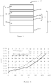
- the figure 2 represents a semiconductor structure 1 based on III-N materials in accordance with the invention.
- the semiconductor structure 1 can take the form of a circular semiconductor wafer of standardized dimension, for example 150 mm, 200 mm or even 300 mm. But the invention is in no way limited to this shape or to these dimensions. Thus, in the case where the semiconductor structure 1 is part of a single integrated device, finished or semi-finished, it will take the form of a block of material, rectangular or square, from a few millimeters to a few centimeters apart. , to the dimensions of the integrated device.
- the semiconductor structure 1 comprises a support substrate 2 capable of receiving crystalline layers of III-N material, by epitaxy.
- the support substrate 2 is advantageously made of monocrystalline silicon, and preferably of crystalline orientation (111).
- the invention is not limited to this material and to this orientation, alternatively, it can be silicon carbide, solid gallium nitride, silicon (110) or (001) or even a substrate advanced type silicon-on-insulator or silicon carbide-on-insulator.
- the structure 1 also comprises, on the support substrate 2, a main monocrystalline layer 3 made of III-N material.
- the main layer 3 comprises a first section 3a disposed on the support 2 and a second section 3b disposed on the first section 3a.
- sections 3a, 3b can have different compositions from one another.
- each section 3a, 3b can also be composed of a plurality of sublayers of different composition or nature from one another.
- the main layer 3 provides a thickness of material making it possible to move away from the support substrate 2 an integrated device formed on the structure 1.
- the intensity of the electric field which develops between the support substrate 2 and the source electrode S is thus limited. or drain D, for a given voltage, when this device is in operation.
- the thickness of the main layer 3 (that is to say the thickness of material between the upper face of the support substrate 2 and the free face of the semiconductor structure 1) is greater than 3 microns, or 5 microns or 10 microns.
- a large thickness makes it possible to form on the semiconductor structure 1 an integrated device which can be subjected to a high voltage without the risk of breaking down (for example greater than 1000 V).
- the main layer 3 is doped to make it resistive. It could be for example a carbon doping whose concentration in the main layer may be between 5 ⁇ 10 ⁇ 18 and 5 ⁇ 10 ⁇ 19 at / cm ⁇ 3. It may also be another p-type doping, for example with iron or magnesium.
- This concentration is not necessarily uniform in the main layer 3 and in the sections of the main layer 3a, 3b. It can vary within this layer and / or these sections 3a, 3b, in particular in a direction perpendicular to the support substrate 2.
- the section 3a of the main layer 3 which is in contact with the support substrate 2 may comprise in contact with this support 2 a first nucleation sublayer of a few hundred nm thick, for example in AlN (not shown on figure 2 ), facilitating the epitaxy of the rest of the main layer 3 on the support substrate 2.
- This AlN nucleation sub-layer is particularly useful when the support 2 is made of silicon.
- Section 3a may also comprise, on the nucleation sublayer, one or more other sublayers, for example GaN or AlGaN, of homogeneous composition or in the form of a superlattice (these terms will be defined later).
- the difference in the thermal expansion coefficients that may exist between the support substrate 2 and the main monocrystalline layer 3 can lead to the generation of significant stresses in these elements during the temperature formation of the main layer 3 and / or following its formation, and more particularly during the cooling of the structure.
- the support substrate 2 has a thermal expansion coefficient lower than that of the main layer 3, this layer is subjected, after its temperature formation and its return to ambient temperature, to extensive stresses which may lead to its cracking. This is particularly the case when the layer main 3 has a thickness greater than a few microns.
- the invention provides, interposed in the main layer 3, a monocrystalline interlayer 4 in III-N material disposed between the first section 3a and the second section 3b.
- This intermediate layer 4 is configured to compress the second section 3b of the main layer 3, during its temperature formation (by epitaxy). This compression compensates, when returning to ambient temperature, for the extensive stresses that may lead to its cracking when the support substrate 2 has a thermal expansion coefficient lower than the main layer 3.
- the intermediate layer 4 is composed of a lower layer 4a disposed on the first section 3a of the main layer 3 and of an upper layer 4b disposed on, and in contact with, the lower layer 4a.
- the nature and the composition of the intermediate layer 4 are chosen so that the mesh parameter of the material forming the lower layer 4a is smaller than the parameter of mesh of the material forming the upper layer 4b. This is chosen to be smaller than the mesh parameter of the material forming the second section 3b.
- the upper layer 4b is directly in contact with the lower layer 4a.
- the expression “mesh parameter of a layer of material” designates the mesh parameter of the material, in the plane defined by the layer.
- the lower layer 4a can consist of a layer of homogeneous composition. Alternatively, it can be made up of a super network. In both cases, the main function of this lower layer 4a is to compress the second section 3b of the main layer 3. To promote this compression, and as is recalled in the document US2006 / 0191474 of the state of the art, the lower layer 4a is formed at a first relatively low temperature, for example less than 1000 ° C. Consequently, it exhibits a lower crystalline quality, and in particular exhibits a concentration of through-dislocations which can reach 10 ⁇ 10 or 10 ⁇ 11 / cm ⁇ 2, as can be determined by a TEM or SEM analysis.
- This concentration is much higher than the concentration of dislocations present in layers obtained at a second more conventional temperature, greater than 1000 ° C and typically between 1050 ° C and 1100 ° C approximately during the formation by MOCVD of layers of III materials. -NOT. These dislocations form privileged passages for the current, and therefore lead to a reduction in the electrical resistivity of the structure.
- the intermediate layer 4 also comprises an upper layer 4b, consisting of a super network.
- the top layer 4b is formed at a second more conventional temperature, higher than the first temperature. It can thus be greater than 1000 ° C, and typically between 1050 ° C and 1100 ° C.
- the upper layer 4b has a lower dislocation density than that of the lower layer 4a. Besides its contribution to the stressing of the second section 3b of the main layer, the upper layer is particularly effective in improving the electrical properties of the stack and compensating for the electrical faults of the lower layer 4a on which it rests.
- super network and according to the usual definition in the semiconductor field, is meant a periodic stack of thin layers, for example between 0.5 and 20 nm, or even 50 nm.
- a layer formed in a superlattice can be assimilated, macroscopically, to a layer of homogeneous composition, as can be revealed by ray diffraction analysis, by photo- or by cathodoluminescence. It is specified that the lattice parameter of a superlattice layer corresponds to the lattice parameter of the equivalent homogeneous layer (whose composition can be revealed by X-ray diffraction, by photo- or by cathodoluminescence).
- the lower layer is advantageously doped (p type) to make them resistive. It can be a carbon, iron or magnesium doping in a concentration which can be between 5 ⁇ 10 ⁇ 18 and 5 ⁇ 10 ⁇ 19 at / cm ⁇ 3.
- the upper layer, arranged on the lower layer consists of a super network (AlGaN / GaN super lattice) and comprises a p-type dopant of carbon, iron or magnesium in a concentration of between 5X 10 18 and 5X 10 19 at / cm 3 .
- the intermediate layer 4 has a thickness which may be between 200 nm and 1000 nm in order to maintain the effective compression of the parts of section 3b of the main layer 3, without requiring an excessive thickness.
- each of the upper and lower layers 4a, 4b can have a thickness of between 10 and approximately 1000 nm.
- both the lower layer 4a and the upper layer 4b are superlattices, these have different through-dislocation densities, so that it is well possible to distinguish two distinct layers from one of them. other in the stack.
- top layer 4b is a superlattice rather than as a homogeneous layer.
- the upper layer 4b produced in the form of superlattices prevents the appearance of these defects even when these layers are doped at high concentration.
- at least this layer is doped at high concentration with a p-type dopant of carbon, iron or magnesium in a concentration of between 5 ⁇ 10 18 and 5 ⁇ 10 19 at / cm 3 . It is then possible to provide an intermediate layer 4 and a very resistive semiconductor structure 1 which limit the leakage currents of an integrated device formed on this structure 1.
- the numerous interfaces which make up the stack of layers forming the superlattice appear to be beneficial to the insulation and limitation of the leakage currents of the semiconductor structure 1. They prevent or in particular limit the appearance of a plane.
- conductive electronics which promotes the flow of leakage currents
- the intermediate layer 4 which sometimes appears when the intermediate layer 4 consists of a homogeneous layer (forming a heterojunction with the underlying layer) of the state of the art.
- the upper superlattice layer 4b forms an effective barrier to the free carriers of the semiconductor structure.
- the super network constituting the upper layer 4b and, where appropriate, the lower layer 4a can be formed from a repetition of a pattern, the pattern comprising at least two layers.
- the natures of the two layers are different, that is to say that at least two of the couples (w1, w2); (x1, x2); (y1, y2); (z1, z2) are different.
- Each layer making up the pattern has a very small thickness, according to the invention of between 0.5 nm and 50 nm.
- these layer thicknesses will be chosen so as to be less than their critical thicknesses and to limit the formation of dislocations.
- the invention is not limited to this form of super network, and a certain degree of relaxation can be provided in the layers.
- the thicknesses of the layers of the pattern may be identical to one another or different.
- the pattern constituting the upper layer 4b can be repeated from 2 to 500 times, depending on the respective thicknesses of the layers which compose it, so as to form an upper layer 4b with a thickness of between 10 and approximately 1000 nanometers.
- the intermediate layer 4 is preferably placed centrally in the thickness of the main layer 3, that is to say that the thicknesses of the first section 3a and of the second section 3b can be substantially identical (to within 50%). This effectively controls the stresses that develop in the material during its manufacture.
- the semiconductor structure 1 can have more than one interlayer, in particular when the thickness of the main layer 4 is large, in particular greater than 5 microns.
- FIG 3 shows a semiconductor structure 1 'comprising a structure 1 in all points similar to that shown in figure 2 which has just been described in detail.
- a second intermediate single-crystal layer 4c has been formed, on which is placed a third section 3c of the main single-crystal layer 3.
- the second intermediate layer 4c puts the third section 3c of the main layer in compression.
- the material that makes up the second interlayer has a lower mesh parameter than the material that makes up the third section 3c of the main layer.
- the second intermediate layer 4c can take any suitable form: it can be composed or constituted of a homogeneous layer, of a super network, or of a combination of such elements. It can in particular be composed of a lower layer and an upper layer similar to what has been described in relation to intermediate layer 4.
- the semiconductor structure 1, 1 'of the invention is produced by growth, for example by vapor phase epitaxy (“Metal Organic Chemical Vapor Deposition” according to the English terminology) or by epitaxy by molecular beams (“Molecular Beam Epitaxy” according to the English terminology).
- the support substrate 2 (or a plurality of support substrates) is placed in a deposition chamber of conventional equipment.
- the support substrate 2 can be prepared before deposition in order to remove a layer of native oxide from its surface.
- the chamber is crossed by a flow of precursor and carrier gas, at a temperature typically between 1050 ° C and 1150 ° C for most of the layers making up the structure, and maintained at a temperature pressure of the order of 100 mbar, and typically between 50 and 200 mbar.
- the growth conditions that is to say the temperature, the pressure, the gas flows make it possible to choose the composition, the quality and the thickness of each element of the stack forming the structure 1, 1 '.
- the lower layer 4a is formed at a first relatively low temperature, lower than the formation temperature of the upper layer 4b, so as to promote the stressing of the second section 3b of the main layer. 3.
- the precursor gas of the element Ga can be tri-methylgallium (of composition Ga (CH 3 ) 3 ) or tri-ethylgallium (of composition Ga (C 2 H 5 ) 3 );
- the precursor gas of the element Al can be tri-methylaluminum (of composition Al 2 (CH 3 ) 6 ) or tri-ethylaluminum (of composition Al 2 (C 2 H 5 ) 6 ),
- the precursor of the element III can be ammonia (NH3); and the carrier gas may comprise or consist of hydrogen and / or nitrogen.
- the growth conditions also make it possible to control the proportion of carbon which is incorporated into the layers during the growth for inherently doping them.
- an additional p-type extrinsic doping source can be used to make certain layers resistive. It may be a source of dopant with iron, carbon or even magnesium.
- the source of extrinsic doping can be CCl 4 , CBr 4 , C2H2, C2H4, C6H12, etc.
- a 200 mm silicon 111 wafer is placed. First of all, an AlN nucleation layer of 100 to 300 nm is formed on this wafer. thickness. Then a main layer of 5 microns of GaN is formed on the nucleation layer. Interleaved in this main layer, there is formed, two microns from the support, an intermediate layer 4.
- This intermediate layer consists of a lower layer 4a of homogeneous AlN constitution 17 nm thick. This layer has a dislocation density greater than 10 ⁇ 10 / cm ⁇ 2.
- an upper layer 4b is formed in the form of a superlattice composed of 100 repetitions of a pattern formed by a first layer of AlGaN having an Al concentration of 20% of 1 nm of thickness, and a second GaN layer of 1 nm thick.
- This layer has a dislocation density of less than 10 ⁇ 10 / cm ⁇ 2.
- the intermediate layer 4 therefore has a thickness of 217 nm and the upper layer 4b in a superlattice can be assimilated macroscopically to a homogeneous AlGaN layer, the aluminum content of which is 10%.
- the AlN layer forming the lower layer and, to a certain extent, the superlattice forming the upper layer 4b, have a lattice parameter smaller than that of the GaN constituting the main layer 3 and make it possible to maintain the section of this main layer 3.
- the main layer 3 and the intermediate layers 4a, 4b are all doped with carbon, in a concentration of the order of 10 ⁇ 19 at / cm ⁇ 3 during their growth.
- the main GaN layer 3 has a satisfactory crystalline quality, in particular it does not exhibit any crack which would make it unsuitable for receiving an integrated device.
- the intermediate layer consists of a lower layer 4a in a super network.
- the lower layer 4a is composed of 10 repetitions of a pattern formed of a first layer of AlN 1 nm thick and a second layer of GaN 0.5 nm thick.
- the lower superlattice layer 4a can be assimilated macroscopically to a homogeneous layer of AlGaN 15 nm thick, the aluminum content of which is 66%.
- This example relates to a semiconductor structure having two interlayer layers.
- a second interlayer consisting of a homogeneous layer of AlGaN having a concentration of 80% aluminum and 20 nm thick.
- a third section of GaN is formed, having a thickness of 1 micron.
- the second interlayer consists of a super network.
- the superlattice is formed of 5 repeats of a pattern formed of a 2 nm AlN layer and a 2 nm AlGaN (60% Al) layer.
- Example 1 This counterexample is similar to the structure of Example 1 in which the upper superlattice layer 4b has been replaced by a homogeneous upper layer of AlGaN (with an aluminum content of 10%) of 200 nm.
- the only difference between the semiconductor structure of Example 1 and Counter-Example 1 is that in Example 1 the top layer is made in the form of a superlattice, and in counter-example 1, the upper layer is produced in the form of a homogeneous layer.
- the figure 4 graphically illustrates the leakage current density performance of the structure of Example 1 and the structure of Counter-Example 1.
- the x-axis represents a vertical voltage (expressed in volts) applied to either side of the structure, i.e. between the free face of the support substrate 2 on the one hand and the free face on the other hand of the main layer 3.
- the y-axis represents the current density flowing between these two surfaces (expressed in Ampere / mm ⁇ 2 and on a logarithmic scale).
- the leakage current density according to the voltage applied in the case of the semiconductor structure of Example 1 is represented on this graph by the solid line.
- the leakage current density according to the voltage applied in the case of the semiconductor structure of counterexample 1 is represented on this graph by the dotted line. The measurements were carried out at room temperature.
- Example 1 makes it possible to gain approximately one decade of current density, whatever the voltage applied up to at least 1000 volts. It is therefore understood that an integrated device (such as a HEMT device) having a determined geometry formed on the structure of Example 1 will have a leakage current approximately ten times less than the same device, therefore having the same geometry, and formed on the structure of counterexample 1.
- an integrated device such as a HEMT device
- the semiconductor structure 1 has been illustrated in a power application when it is provided with an integrated device of the HEMT type, the invention is in no way limited to this application or to this type of. device. Thus, it is possible to take advantage of the semiconductor structure 1 of the invention in the field of radiofrequencies, of light-emitting diodes and for any other application or device for which the electrical properties presented are advantageous.
Landscapes
- Junction Field-Effect Transistors (AREA)
- Chemical & Material Sciences (AREA)
- Crystallography & Structural Chemistry (AREA)
- Crystals, And After-Treatments Of Crystals (AREA)
- Chemical Vapour Deposition (AREA)
- Engineering & Computer Science (AREA)
- Materials Engineering (AREA)
- Inorganic Chemistry (AREA)
Description
- La présente invention concerne une structure semi-conductrice à base de matériaux III-N.
- Les structures semi-conductrices à base de matériaux III-N sont notamment utiles pour recevoir des transistors du type HEMT (« High Electron Mobility Transistor » selon la terminologie anglo-saxonne ou transistor à haute mobilité d'électrons) qui trouvent leur application par exemple comme interrupteur dans les convertisseurs de puissance.
- On connaît du document « High electron mobility transistor based on a GaN-AlGaN heterojunction » M.A. Kahn et al., Applied Physics Letters, Vol. 63, N°9 du 30 août 1993, une structure semi-conductrice 1 munie d'un tel transistor HEMT. Comme cela est représenté schématiquement sur la
figure 1 , cet ensemble est composé : - d'un substrat de saphir 2 et d'une couche principale d'AlN 3 formant la structure semi-conductrice 1 ;
- d'une hétérojonction constituée d'une couche canal 5 en GaN et d'une couche barrière 6 d'AlGaN formées successivement sur la structure semi-conductrice ;
- d'électrodes de source S, de drain D et de grille G sur/dans l'hétérojonction.
- L'état électriquement passant du transistor entre la source S et le drain D est commandé par la tension appliquée à la grille G.
- Ainsi, lorsque la tension appliquée sur la grille G excède une tension seuil Vt, le transistor est passant. Dans le cas d'application de puissance, plusieurs ampères voire plusieurs dizaines d'ampères peuvent circuler dans la couche canal entre la source S et le drain D. La tension VDS qui se développe dans ce cas entre ces deux électrodes est de l'ordre de quelques volts à quelques dizaines de volts, et est liée à la résistivité du matériau de la couche canal.
- Lorsque la tension appliquée sur la grille G est inférieure à la tension seuil Vt, le transistor est bloquant. Dans le cas d'application de puissance, la tension VDS qui s'applique aux bornes des électrodes de source S et de drain D peut alors atteindre quelques centaines de volts à quelques milliers de volts. Le courant de fuite circulant entre la source S et le drain D est faible, de l'ordre de quelques nanoampères par mm de largeur de grille.
- En contrôlant la tension de grille, le transistor peut être commuté très rapidement (en quelques nanosecondes) entre un état passant et un état bloquant.
- Plusieurs problèmes limitent toutefois la diffusion de cette technologie.
- Comme on l'a vu, à l'état bloquant, une forte tension s'applique aux bornes des électrodes de source S et de drain D. Cela conduit à la formation d'un champ électrique dont les lignes pénètrent très en profondeur dans la couche principale 3 et le substrat 2. Un champ électrique qui peut être d'intensité importante se développe alors entre l'électrode de drain D et le substrat 2, notamment dans l'épaisseur de la couche principale 3, et entre la source S et le drain D. Afin d'éviter que l'intensité de ce champ n'excède la valeur critique (appelée champ de claquage) au-delà duquel le matériau ne peut plus le soutenir, on doit prévoir de séparer le drain D et la source S d'une distance suffisante d pour que, pour une tension donnée VDS, l'intensité du champ E = VDS/d soit inférieur au champ de claquage. De la même manière, on doit prévoir de fournir une couche principale 3 d'épaisseur suffisante pour que la tension qui se développe entre le substrat 2 et le drain D (qui peut être de l'ordre de VDS) conduisent à une intensité du champ dans les matériaux en jeu qui soit également inférieure au champ de claquage.
- Il est relativement aisé de choisir la distance d séparant l'électrode de drain D de la source S lors de la conception du transistor. Ainsi, pour une tension VDS de l'ordre de 400 V à 2000 V, on peut choisir une distance d de l'ordre de 5 à 20 microns.
- Fournir une structure semi-conductrice 1 présentant une couche principale 3 en matériaux III-N suffisamment épaisse (de l'ordre de 3 microns ou plus) est toutefois bien plus difficile, notamment lorsque le substrat 2 est choisi en silicium plutôt qu'en saphir, pour des raisons de disponibilité et de coût.
- À ce titre, les documents
EP1290721 etWO2013001014 fournissent des exemples de techniques connues permettant de faire croître une couche principale 3 épaisse d'un matériau III-N sur un substrat 2 qui peut être en silicium. Ces techniques comprennent l'insertion dans la couche tampon en matériaux III-N d'au moins une couche intercalaire, également en matériau III-N, dont la nature est choisie pour mettre en compression une partie de la couche tampon avec laquelle elle est en contact. - Un autre problème qui limite la diffusion de la technologie, concerne le courant de fuite circulant, dans l'épaisseur de la couche principale 3, entre la source S et le drain D lorsque le transistor est à l'état bloquant. Bien entendu, on souhaiterait que ce courant soit le plus petit possible. C'est pourquoi la couche principale 3 est généralement dopée à l'aide d'un dopant de type p, tel que du fer, du carbone ou du magnésium, pour la rendre résistive et limiter de la sorte la circulation des courants de fuite.
- L'expérience montre toutefois que malgré ce dopage résistif, la structure 1 peut présenter un courant de fuite excessif pour les applications visées.
-
US 8 405 064 B2 décrit des structures épitaxiales de GaN sur Si, où des super-réseaux de AlN/GaN sont insérés pour induire une contrainte compressive qui contre la contrainte en tension causée par la différence entre les coefficients de dilatation thermique des nitrures de groupe III et du Si. -
EP 2 767 620 A1 voirfigure 2 décrit des structures épitaxiales de GaN sur Si, avec une couche intercalaire 230 ciblant la réduction des contraintes en tension induites par l'inadéquation de l'expansion thermique entre le film de nitrure III et le substrat de Si. Le document enseigne l'emploi de dopage avec du carbone ou du magnésium dans la couche intercalaire pour combattre la formation de canaux conductifs parasitaires. Le document (voir paragraphe [0050]) enseigne aussi l'emploi d'un super-réseau 250 dopé avec du carbone comme couche tampon entre l'hétéro-substrat et la couche principale 220-240. - On connaît également des documents « Stress control in GaN grown on silicon (111) by metalorganic vapor phase eptitaxy », de E. Feltin et al., Applied Physics Letters, Vol. 79, n°20 du 12 novembre 2001 ;
US2006191474 etWO0229873 - La présente invention vise à pallier tout ou partie des inconvénients précités. Elle vise en particulier à fournir une structure semi-conductrice présentant, sur un substrat support, une couche principale épaisse et très résistive afin de pouvoir former un transistor pouvant supporter des tensions importantes, et limitant l'intensité des courants de fuite.
- En vue de la réalisation de l'un de ces buts, l'objet de l'invention propose une structure semi-conductrice à base de matériaux III-N selon la revendication 1; et son procédé de fabrication selon la revendication 9.
- D'autres caractéristiques et avantages de l'invention ressortiront de la description détaillée de l'invention qui va suivre en référence aux figures annexées sur lesquelles :
- la
figure 1 représente une structure semi-conductrice munie d'un transistor HEMT selon l'état de la technique ; - la
figure 2 représente une structure semi-conductrice à base de matériaux III-N conforme à l'invention; - la
figure 3 représente une autre structure semi-conductrice à base de matériaux III-N conforme à l'invention; - la
figure 4 illustre graphiquement les performances en courant de fuite d'une structure semi-conductrice conforme à l'invention. - Par souci de simplification de la description à venir, les mêmes références sont utilisées pour des éléments identiques ou assurant la même fonction dans les différents modes de mise en œuvre de l'invention ou dans l'exposé de l'état de la technique.
- La
figure 2 représente une structure semi-conductrice 1 à base de matériaux III-N conforme à l'invention. - La structure semi-conductrice 1 peut prendre la forme d'une plaquette de semi-conducteur circulaire de dimension normalisée par exemple de 150 mm, 200 mm voire même 300 mm. Mais l'invention n'est nullement limitée à cette forme ou à ces dimensions. Ainsi, dans le cas où la structure semi-conductrice 1 fait partie d'un dispositif intégré singularisé, fini ou semi-fini, elle prendra la forme d'un bloc de matériau, rectangulaire ou carré, de quelques millimètres à quelques centimètres de côté, aux dimensions du dispositif intégré.
- Quelle que soit sa forme, la structure semi-conductrice 1 comprend un substrat support 2 apte à recevoir des couches cristallines en matériau III-N, par épitaxie. Pour des raisons de coût et de disponibilité, le substrat support 2 est avantageusement en silicium monocristallin, et de préférence d'orientation cristalline (111). Mais l'invention n'est pas limitée à ce matériau et à cette orientation, alternativement, il peut s'agir de carbure de silicium, de nitrure de gallium massif, de silicium (110) ou (001) ou encore d'un substrat avancé du type silicium sur isolant ou carbure de silicium sur isolant.
- La structure 1 comprend également, sur le substrat support 2, une couche principale 3 monocristalline en matériau III-N. Par matériau III-N, on entend tout matériau, alliage ou empilement de matériau ou d'alliage de la forme générique BwAlxGayInzN avec w+x+y+z=1. La couche principale 3 comporte une première section 3a disposée sur le support 2 et une seconde section 3b disposée sur la première section 3a.
- La nature de la couche principale 3 n'est pas nécessairement identique sur toute son épaisseur. Ainsi, les sections 3a, 3b peuvent présenter des compositions différentes l'une de l'autre. Par ailleurs, chaque section 3a, 3b peut également être composée d'une pluralité de sous-couches de composition ou de nature différentes les unes des autres.
- La couche principale 3 fournit une épaisseur de matériau permettant d'éloigner du substrat support 2 un dispositif intégré formé sur la structure 1. On limite ainsi l'intensité du champ électrique qui se développe entre le substrat support 2 et l'électrode de source S ou de drain D, pour une tension donnée, lorsque ce dispositif est en fonctionnement.
- De manière avantageuse, l'épaisseur de la couche principale 3 (c'est-à-dire l'épaisseur de matériau comprise entre la face supérieure du substrat support 2 et la face libre de la structure semi-conductrice 1) est supérieure à 3 microns, ou 5 microns ou 10 microns. Une épaisseur importante permet de former sur la structure semi-conductrice 1 un dispositif intégré qui peut être soumis à une tension importante sans risquer de claquer (supérieure par exemple à 1000 V).
- Préférentiellement, et afin de limiter les courants de fuite pouvant circuler dans la structure 1 lorsque celle-ci est munie d'un dispositif intégré, la couche principale 3 est dopée pour la rendre résistive. Il peut s'agir par exemple d'un dopage au carbone dont la concentration dans la couche principale peut être comprise entre 5×10^18 et 5×10^19 at/cm^3. Il peut s'agir également d'un autre dopage de type p, par exemple au fer ou au magnésium.
- Cette concentration n'est pas nécessairement uniforme dans la couche principale 3 et dans les sections de la couche principale 3a, 3b. Elle peut varier au sein de cette couche et/ou de ces sections 3a, 3b, notamment selon une direction perpendiculaire au substrat support 2.
- A titre d'exemple, la section 3a de la couche principale 3 qui est en contact avec le substrat support 2 peut comprendre en contact avec ce support 2 une première sous-couche de nucléation de quelques centaines de nm d'épaisseur, par exemple en AlN (non représenté sur la
figure 2 ), facilitant l'épitaxie du reste de la couche principale 3 sur le substrat support 2. Cette sous-couche de nucléation en AlN est particulièrement utile lorsque le support 2 est en silicium. La section 3a peut également comprendre, sur la sous-couche de nucléation, une ou plusieurs autres sous-couches, par exemple du GaN ou de AlGaN, de composition homogène ou sous la forme de super réseau (ces termes seront définis ultérieurement). - Comme cela est rappelé dans les documents présentés de l'état de la technique, la différence des coefficients de dilatation thermique pouvant exister entre le substrat support 2 et la couche principale 3 monocristalline peut conduire à la génération de contraintes importantes dans ces éléments au cours de la formation en température de la couche principale 3 et/ou suite à sa formation, et tout particulièrement lors du refroidissement de la structure. Lorsque le substrat support 2 présente un coefficient de dilatation thermique inférieur à celui de la couche principale 3, cette couche est soumise, après sa formation en température et son retour à température ambiante, à des contraintes extensives pouvant conduire à sa fissuration. C'est notamment le cas lorsque la couche principale 3 présente une épaisseur supérieure à quelques microns.
- Afin de limiter cet effet et prévenir l'apparition de fissures dans la couche principale 3 qui rendraient la structure semi-conductrice 1 inapte à recevoir un dispositif intégré, l'invention prévoit, intercalée dans la couche principale 3, une couche intercalaire 4 monocristalline en matériau III-N disposée entre la première section 3a et la seconde section 3b. Cette couche intercalaire 4 est configurée pour mettre en compression la seconde section 3b de la couche principale 3, au cours de sa formation en température (par épitaxie). Cette compression compense lors du retour à température ambiante les contraintes extensives pouvant conduire à sa fissuration lorsque le substrat support 2 présente un coefficient de dilatation thermique inférieure à la couche principale 3.
- Selon l'invention, la couche intercalaire 4 est composée d'une couche inférieure 4a disposée sur la première section 3a de la couche principale 3 et d'une couche supérieure 4b disposée sur, et en contact avec, la couche inférieure 4a.
- Pour permettre la mise en compression efficace de la seconde section 3b de la couche principale 3, la nature et la composition de la couche intercalaire 4 sont choisies pour que le paramètre de maille du matériau formant la couche inférieure 4a soit plus petit que le paramètre de maille du matériau formant la couche supérieure 4b. Celui-ci est choisi pour être plus petit que le paramètre de maille du matériau formant la seconde section 3b. Pour la même raison de mise en compression efficace de la seconde section 3b de la couche principale 3, la couche supérieure 4b est directement en contact avec la couche inférieure 4a. Par souci de clarté, on précise que l'expression « paramètre de maille d'une couche de matériau» désigne le paramètre de maille du matériau, dans le plan défini par la couche.
- La couche inférieure 4a peut être constituée d'une couche de composition homogène. Alternativement, elle peut être constituée d'un super réseau. Dans les deux cas, cette couche inférieure 4a a pour fonction principale de mettre en compression la seconde section 3b de la couche principale 3. Pour favoriser cette mise en compression, et comme cela est rappelé dans le document
US2006/0191474 de l'état de la technique, la couche inférieure 4a est formée à une première température relativement basse, par exemple inférieure à 1000°C. En conséquence, elle présente une qualité cristalline moindre, et présente notamment une concentration de dislocations traversantes pouvant atteindre 10^10 ou 10^11/cm^2, comme cela peut être déterminé par une analyse TEM ou SEM. Cette concentration est bien supérieure à la concentration de dislocations présente dans des couches obtenues à une seconde température plus conventionnelle, supérieure à 1000°C et typiquement comprise entre 1050°C et 1100°C environ lors de la formation par MOCVD de couches en matériaux III-N. Ces dislocations forment des passages privilégiés pour le courant, et conduisent donc à réduire la résistivité électrique de la structure. - C'est pourquoi, selon l'invention, la couche intercalaire 4 comprend également une couche supérieure 4b, constituée d'un super réseau. La couche supérieure 4b est formée à une seconde température plus conventionnelle, supérieure à la première température. Elle peut être ainsi supérieure à 1000°C, et typiquement comprise entre 1050°C et 1100°C. La couche supérieure 4b présente une densité de dislocation inférieure à celle de la couche inférieure 4a. Outre sa contribution à la mise sous contrainte de la seconde section 3b de la couche principale, la couche supérieure est particulièrement efficace pour améliorer les propriétés électriques de l'empilement et compenser les défauts électriques de la couche inférieure 4a sur laquelle elle repose.
- Par « super réseau », et selon la définition usuelle dans le domaine du semi-conducteur, on entend un empilement périodique de couches de faible épaisseur, par exemple comprises entre 0,5 et 20 nm, voire même 50nm. Comme cela est bien connu en soi, une couche formée en super réseau est assimilable, macroscopiquement, à une couche de composition homogène, comme cela peut être révélé par une analyse en diffraction aux rayons, par photo- ou par cathodoluminescence. On précise que le paramètre de maille d'une couche en super réseau correspond au paramètre de maille de la couche homogène équivalente (dont la composition peut être révélée par diffraction aux rayons X, par photo- ou par cathodoluminescence).
- Similairement à ce qui avait été exposé pour la couche principale 3, et pour les mêmes raisons, la couche inférieure est avantageusement dopée (type p) pour les rendre résistives. Il peut s'agir d'un dopage carbone, fer ou magnésium dans une concentration qui peut être comprise entre 5×10^18 et 5×10^19 at/cm^3. Selon l'invention, la couche supérieure, disposée sur la couche inférieure, est constituée d'un super réseau (AlGaN/GaN super lattice) et comprend un dopant de type p de carbone, de fer ou de magnésium dans une concentration comprise entre 5X 10¹⁸ et 5X 10¹⁹ at/cm3.
- Selon l'invention, la couche intercalaire 4 présente une épaisseur qui peut être comprise entre 200 nm et 1000nm afin de conserver la mise en compression effective des parties de la section 3b de la couche principale 3, sans nécessiter une épaisseur excessive. D'une manière générale, chacune des couches supérieure et inférieure 4a, 4b peut présenter une épaisseur comprise entre 10 et environ 1000 nm.
- Dans le cas où à la fois la couche inférieure 4a et la couche supérieure 4b sont des super réseaux, celles-ci présentent des densités de dislocations traversantes différentes, de sorte qu'il est bien possible de distinguer deux couches distinctes l'une de l'autre dans l'empilement.
- Former la couche supérieure 4b sous la forme de super réseau plutôt que sous la forme d'une couche homogène présente de nombreux avantages.
- Tout d'abord, la demanderesse a observé qu'il était possible de doper fortement cette couche (par exemple avec du carbone et dans la gamme précitée de concentration de 5×10^18 à 5×10^19 at/cm^3) sans endommager la qualité cristalline de ces couches.
- Il est en effet parfois observé qu'une concentration importante de dopant dans une couche homogène de matériau III-N, peut conduire à former des trous ou d'autres défauts morphologiques de surface. Ces défauts ont pour conséquence de rendre la structure semi-conductrice qui les contient inapte à recevoir un dispositif intégré, et notamment un dispositif de puissance, performant. Ils conduisent à des courants de fuite importants et une tension de claquage réduite.
- La couche supérieure 4b réalisée sous la forme de super réseaux prévient l'apparition de ces défauts même lorsque ces couches sont dopées à forte concentration. Selon l'invention au moins cette couche est dopée à forte concentration avec un dopant de type p de carbone, de fer ou de magnésium dans une concentration comprise entre 5X 10¹⁸ et 5X 10¹⁹ at/cm3. On peut alors fournir une couche intercalaire 4 et une structure semi-conductrice 1 très résistive qui limitent les courants de fuite d'un dispositif intégré formé sur cette structure 1.
- De plus, les nombreuses interfaces qui composent l'empilement de couches formant le super réseau apparaissent bénéfiques à l'isolation et la limitation des courants de fuites de la structure semi-conductrice 1. Elles préviennent ou limitent notamment l'apparition d'un plan électronique conducteur (qui favorise l'écoulement de courants de fuite) sous la couche supérieure 4b (et sous la couche inférieure 4a lorsque celle-ci est formée d'un super réseau) qui apparaît parfois lorsque la couche intercalaire 4 est constituée d'une couche homogène (formant hétérojonction avec la couche sous-jacente) de l'état de la technique. D'une manière générale, la couche supérieure 4b en super réseau forme une barrière efficace aux porteurs libres de la structure semi-conductrice.
- D'une manière générale, le super réseau constituant la couche supérieure 4b et, le cas échéant, la couche inférieure 4a, peut être formé d'une répétition d'un motif, le motif comprenant au moins deux couches. La première couche présente la forme générale Alw1GaNx1Iny1Bz1N avec w1+x1+y1+z1=1 et la deuxième couche présente la forme générale Alw2GaNx2Iny2Bz2N avec w2+x2+y2+z2=1. Les natures des deux couches sont différentes c'est-à-dire que deux au moins des couples (w1, w2) ; (xl, x2) ;(y1, y2) ; (z1, z2) sont différents.
- Chaque couche composant le motif présente une très faible épaisseur, selon l'invention comprise entre 0,5 nm et 50 nm. De préférence, on choisira ces épaisseurs de couches de manière à être inférieure à leurs épaisseurs critiques et limiter la formation de dislocations. Mais l'invention n'est pas limitée à cette forme de super réseau, et on pourra prévoir un certain degré de relaxation dans les couches. Par ailleurs, les épaisseurs des couches du motif peuvent être identiques entre elles ou différentes.
- Le motif constituant la couche supérieure 4b peut être répété de 2 à 500 fois, suivant les épaisseurs respectives des couches qui la compose, de sorte à former une couche supérieure 4b d'épaisseur comprise entre 10 et environ 1000 nanomètres. Il en va de même pour le motif constituant la couche inférieure 4a, lorsque celle-ci est formée d'un super réseau.
- La couche intercalaire 4 est préférentiellement placée centralement dans l'épaisseur de la couche principale 3, c'est-à-dire que les épaisseurs de la première section 3a et de la seconde section 3b peuvent être sensiblement identiques (à 50% près). On contrôle ainsi de manière efficace les contraintes qui se développent dans le matériau au cours de sa fabrication.
- À titre d'exemple, on peut prévoir d'insérer la couche intercalaire 4 dans la couche principale 3 de sorte que les sections 3a, 3b présentent chacune une épaisseur inférieure à 2 microns, 2,5 microns ou encore 3 microns.
- La structure semi-conductrice 1 peut présenter plus d'une couche intercalaire, notamment lorsque l'épaisseur de la couche principale 4 est importante, en particulier supérieure à 5 microns.
- Ainsi, la
figure 3 représente une structure semi-conductrice 1' comprenant une structure 1 en tout point similaire à celle représentée sur lafigure 2 qui vient d'être décrite en détail. Sur cette structure 1, et plus précisément sur la seconde section 4b de la couche principale, on a formé une seconde couche monocristalline intercalaire 4c, sur laquelle est disposée une troisième section 3c de la couche principale 3 monocristalline. La seconde couche intercalaire 4c met en compression la troisième section 3c de la couche principale. Le matériau qui compose la seconde couche intercalaire présente un paramètre de maille inférieur au matériau qui compose la troisième section 3c de la couche principale. - La seconde couche intercalaire 4c peut prendre toute forme adaptée : elle peut être composée ou constituée d'une couche homogène, d'un super réseau, ou d'une combinaison de tels éléments. Elle peut notamment être composée d'une couche inférieure et d'une couche supérieure similairement à ce qui a été décrit en relation avec couche intercalaire 4.
- On pourra empiler autant de fois que nécessaire, sur la structure semi-conductrice 1, une structure composée d'une couche intercalaire 4c et d'une section 3c pour former une couche principale 3 d'épaisseur importante et de qualité cristalline satisfaisante.
- Quel que soit l'empilement choisi, la structure semi-conductrice 1, 1' de l'invention est réalisée par croissance, par exemple par épitaxie en phase vapeur (« Metal Organic Chemical Vapor Déposition » selon la terminologie anglo-saxonne) ou par épitaxie par jets moléculaires (« Molecular Beam Epitaxy » selon la terminologie anglo-saxonne).
- Pour procéder à la croissance de la couche principale 3 et des couches intercalaires 4a, 4b, 4c on place le substrat support 2 (ou une pluralité de substrats supports) dans une chambre de dépôt d'un équipement conventionnel.
- Comme cela est bien connu en soi, le substrat support 2 peut être préparé avant dépôt pour éliminer une couche d'oxyde natif de sa surface.
- Dans le cas d'un dépôt selon la technologie MOCVD, la chambre est traversée par des flux de gaz précurseur et porteur, en température typiquement comprise entre 1050°C et 1150°C pour la plupart des couches composant la structure, et maintenue à une pression de l'ordre de 100 mbar, et typiquement compris entre 50 et 200 mbar. Les conditions de croissance, c'est à dire la température, la pression, les flux de gaz permettent de choisir la composition, la qualité et l'épaisseur de chaque élément de l'empilement formant la structure 1, 1'. Comme on l'a vu précédemment, la couche inférieure 4a est formée à une première température relativement basse, inférieure à la température de formation de la couche supérieure 4b, de manière à favoriser la mise sous contrainte de la deuxième section 3b de la couche principale 3. Les autres couches de la structure, et notamment la couche supérieure 4b de la couche intercalaire 4 est formée à une température relativement élevée, de l'ordre de 1050°C à 1100°C. A titre d'exemple, le gaz précurseur de l'élément Ga peut être du tri-méthylgallium (de composition Ga(CH3)3) ou du tri-éthylgallium (de composition Ga(C2H5)3) ; le gaz précurseur de l'élément Al peut être du tri-méthylaluminium (de composition Al2(CH3)6) ou de tri-éthylaluminium (de composition Al2(C2H5)6), le précurseur de l'élément III peut être de l'ammoniac (NH3) ; et le gaz porteur peut comprendre ou être constitué d'hydrogène et/ou d'azote.
- Lorsqu'au moins un gaz précurseur est carboné, comme ceux qui ont été listés à titre d'exemple ci-dessus, les conditions de croissance permettent également de contrôler la proportion de carbone qui s'incorpore dans les couches au cours de la croissance pour les doper intrinsèquement. Alternativement, on peut utiliser une source de dopage extrinsèque de type p additionnelle pour rendre certaines couches résistives. Il peut s'agir de source de dopant au fer, au carbone ou encore au magnésium. Dans le cas d'un dopage au carbone, la source de dopage extrinsèque peut être du CCl4, CBr4, C2H2, C2H4, C6H12, etc.
- Dans une chambre de dépôt d'un réacteur MOCVD de type Aixtron ou Veeco, on place une plaquette de 200 mm de silicium 111. On forme tout d'abord sur cette plaquette une couche de nucléation d'AlN de 100 à 300 nm d'épaisseur. Puis on forme une couche principale de 5 microns de GaN sur la couche de nucléation. Intercalés dans cette couche principale, on a formé, à deux microns du support, une couche intercalaire 4. Cette couche intercalaire est constituée d'une couche inférieure 4a de constitution homogène d'AlN de 17 nm d'épaisseur. Cette couche présente une densité de dislocation supérieure à 10^10/cm^2. Sur cette couche inférieure 4a, on forme une couche supérieure 4b sous la forme d'un super réseau composé de 100 répétitions d'un motif formé d'une première couche de AlGaN présentant une concentration d'Al de 20% de 1 nm d'épaisseur, et d'une seconde couche de GaN de 1 nm d'épaisseur. Cette couche présente une densité de dislocation inférieure à 10^10/cm^2.
- La couche intercalaire 4 présente donc une épaisseur de 217 nm et la couche supérieure 4b en super réseau est assimilable macroscopiquement à une couche d'AlGaN homogène dont la teneur en aluminium est de 10 %. La couche d'AlN formant la couche inférieure et, dans une certaine mesure, le super réseau formant la couche supérieure 4b, présentent un paramètre de maille plus petit que celui du GaN constituant la couche principale 3 et permettent de maintenir en compression la section de cette couche principale 3.
- Dans cet exemple, la couche principale 3 et les couches intercalaires 4a, 4b sont toutes dopées en carbone, dans une concentration de l'ordre de 10^19 at/cm^3 au cours de leurs croissances. La couche principale 3 de GaN présente une qualité cristalline satisfaisante, elle ne présente notamment pas de fissure qui la rendrait inapte à recevoir un dispositif intégré.
- Cet exemple est identique à l'exemple précédent, mais cette fois la couche intercalaire est constituée d'une couche inférieure 4a en super réseau. Ainsi, la couche inférieure 4a est composée de 10 répétitions d'un motif formé d'une première couche de AlN de 1 nm d'épaisseur et d'une seconde couche de GaN de 0,5 nm d'épaisseur. La couche inférieure 4a en super réseau est assimilable macroscopiquement à une couche d'AlGaN homogène de 15 nm d'épaisseur dont la teneur en aluminium est de 66 %.
- Cet exemple concerne une structure semi-conductrice présentant deux couches intercalaires. Dans l'exemple 3, on forme sur la structure semi-conductrice de l'exemple 1 une seconde couche intercalaire constituée d'une couche homogène d'AlGaN présentant une concentration de 80% d'aluminium et d'épaisseur 20 nm. Sur la couche d'AlGaN on forme une troisième section de GaN présentant 1 micron d'épaisseur.
- Cet exemple est une structure alternative à celle présentée à l'exemple 3. Dans cet exemple 4, la seconde couche intercalaire est constituée d'un super réseau. Le super réseau est formé de 5 répétitions d'un motif formé d'une couche d'AlN de 2 nm et d'une couche d'AlGaN (60% d'Al) de 2 nm.
- Ce contre-exemple est similaire à la structure de l'exemple 1 dans laquelle la couche supérieure 4b en super réseau a été remplacée par une couche supérieure homogène d'AlGaN (de teneur en Aluminium de 10%) de 200 nm. En d'autres termes, la seule différence entre la structure semi-conductrice de l'exemple 1 et du contre-exemple 1 est que dans l'exemple 1 la couche supérieure est réalisée sous la forme d'un super réseau, et que dans le contre-exemple 1, la couche supérieure est réalisée sous la forme d'une couche homogène.
- La
figure 4 illustre graphiquement les performances en densité de courant de fuite de la structure de l'exemple 1 et de la structure du contre-exemple 1. - L'axe des abscisses représente une tension verticale (exprimée en volts) appliquée de part et d'autre de la structure, c'est à dire entre d'une part la face libre du substrat support 2 et d'autre part la face libre de la couche principale 3. L'axe des ordonnées représente la densité de courant circulant entre ces deux surfaces (exprimée en Ampère/mm^2 et sur une échelle logarithmique).
- La densité de courant de fuite suivant la tension appliquée dans le cas de la structure semi-conductrice de l'exemple 1 est représentée sur ce graphe par le trait plein. La densité de courant de fuite suivant la tension appliquée dans le cas de la structure semi-conductrice du contre-exemple 1 est représentée sur ce graphe par le trait pointillé. Les mesures ont été réalisées à température ambiante.
- On observe que la structure de l'exemple 1 permet de gagner environ une décade de densité de courant, quelle que soit la tension appliquée jusqu'au moins 1000 Volts. On comprend donc qu'un dispositif intégré (tel qu'un dispositif HEMT) présentant une géométrie déterminée formé sur la structure de l'exemple 1 présentera un courant de fuite environ dix fois moindre que le même dispositif, présentant donc la même géométrie, et formé sur la structure du contre-exemple 1.
- Bien qu'on ait illustré les bénéfices de la structure semi-conductrice 1 dans une application de puissance lorsqu'elle est munie d'un dispositif intégré de type HEMT, l'invention n'est nullement limitée à cette application ou à ce type de dispositif. Ainsi, on pourra tirer profit de la structure semi-conductrice 1 de l'invention dans le domaine des radiofréquences, des diodes électroluminescentes et pour tout autre application ou dispositif pour lesquels les propriétés électriques présentées sont avantageuses.
Claims (11)
- Structure semi-conductrice (1) à base de matériaux III-N comprenant :• un substrat support (2) ;• une couche principale (3) en matériau III-N, la couche principale (3) comportant une première section (3a) disposée sur le substrat support (2) et une seconde section (3b) disposée sur la première section (3a);• une couche intercalaire (4) en matériau III-N disposée entre la première section (3a) et la seconde section (3b), pour mettre en compression la seconde section (3b) de la couche principale ; la couche intercalaire (4) étant composée :• d'une couche inférieure (4a) disposée sur la première section (3a) de la couche principale (3) ;• et, disposée sur et en contact avec la couche inférieure (4a), d'une couche supérieure (4b) constituée d'un super réseau ; la couche inférieure (4a) étant constituée d'une couche homogène ou d'un super réseau différent du super réseau constituant la couche supérieure (4b), présentant une densité de dislocation supérieure à celle de la couche supérieure (4b) et un paramètre de maille plus petit que le paramètre de maille du matériau formant la couche supérieure (4b), le super réseau constituant la couche supérieure (4b) et, le cas échéant, le super réseau constituant la couche inférieure (4a), étant formé(s) d'une répétition d'un motif comprenant au moins deux couches de natures différentes, la structure semi-conductrice à base de matériaux III-N étant caractérisé en ce que chaque couche composant le motif présente une 35 épaisseur comprise entre 0,5 nm et 50 nm, la couche intercalaire présente une épaisseur comprise entre 200 nm et 1000 nm, et la couche supérieure comprend un dopant de type p de carbone, de fer ou de magnésium dans une concentration comprise entre 5X 10¹⁸ et 5X 10¹⁹ at/cm3 pour la rendre résistive.
- Structure semi-conductrice (1) selon la revendication précédente dans lequel paramètre de maille du matériau formant la couche supérieure (4b) est plus petit que le paramètre de maille du matériau formant la seconde section (3b) de la couche principale (3).
- Structure semi-conductrice (1) selon l'une des revendications précédentes dans laquelle la couche principale (3) et la couche intercalaire (4) sont monocristallines.
- Structure semi-conductrice (1) selon l'une des revendications précédentes comportant une seconde couche intercalaire (4c) sur la seconde section (3b) de la couche principale (3) et une troisième section (3c) de la couche principale disposée sur la seconde couche intercalaire (4c).
- Structure semi-conductrice (1) selon la revendication précédente dans laquelle la seconde couche intercalaire est composée d'une couche homogène, d'un super réseau, ou d'une combinaison de tels éléments.
- Structure semi-conductrice (1) selon l'une des revendications précédentes dans laquelle le substrat support (2) présente un coefficient de dilatation thermique inférieur à celui de la couche principale (3).
- Plaquette de semi-conducteur comprenant une structure semi-conductrice (1) selon l'une des revendications précédentes.
- Dispositif intégré comprenant une structure semi-conductrice (1) selon l'une des revendications précédentes.
- Procédé de fabrication d'une structure semi-conductrice (1) à base de matériaux III-N sur un substrat support (2), le procédé comprenant :a. la formation d'une couche principale (3) en matériau III-N sur le substrat support (2) la couche principale (3) comportant une première section (3a) et une deuxième section (3b) disposée sur la première section ;b. la formation d'une couche intercalaire (4) en matériau III-N disposée entre la première section (3a) et la seconde section (3b), la couche intercalaire (4) présentant une épaisseur comprise entre 200 nm et 1000nm pour mettre en compression la seconde section (3b) de la couche principale ; la formation de la couche intercalaire (4) comprenant :- la formation, à une première température, d'une couche inférieure (4a) disposée sur la première section (3a) de la couche principale (3) ;- et, la formation, à une seconde température, d'une couche supérieure (4b) constituée d'un super réseau et disposée sur et en contact avec la couche inférieure (4a); la première température étant inférieure à la seconde température, la couche inférieure (4a) étant constituée d'une couche homogène ou d'un super réseau différent du super réseau constituant la couche supérieure (4b), la couche inférieure (4a) présentant un paramètre de maille plus petit que le paramètre de maille du matériau formant la couche supérieure (4b), le super réseau constituant la couche supérieure (4b) et, le cas échéant, le super réseau constituant la couche inférieure (4a), étant formé(s) d'une répétition d'un motif comprenant au moins deux couches de natures différentes, le procédé de fabrication de la structure semi-conductrice à base de matériaux III-N étant caractérisé en ce que chaque couche composant le motif présente une épaisseur comprise entre 0,5 nm et 50 nm, la couche intercalaire présente une épaisseur comprise entre 200 nm et 1000 nm, et la couche supérieure comprend un dopant de type p de carbone, de fer ou de magnésium dans une concentration comprise entre 5X 10¹⁸ et 5X 10¹⁹ at/cm3 pour la rendre résistive.
- Procédé selon la revendication précédente dans lequel la première température est inférieure à 1000°C.
- Procédé selon l'une des revendications 9 et 10 dans lequel la seconde température est comprise entre 1050 et 1100°C.
Applications Claiming Priority (2)
| Application Number | Priority Date | Filing Date | Title |
|---|---|---|---|
| FR1652983A FR3049762B1 (fr) | 2016-04-05 | 2016-04-05 | Structure semi-conductrice a base de materiau iii-n |
| PCT/FR2017/050467 WO2017174885A1 (fr) | 2016-04-05 | 2017-03-01 | Structure semi-conductrice a base de materiau iii-n |
Publications (2)
| Publication Number | Publication Date |
|---|---|
| EP3440692A1 EP3440692A1 (fr) | 2019-02-13 |
| EP3440692B1 true EP3440692B1 (fr) | 2020-07-29 |
Family
ID=56008801
Family Applications (1)
| Application Number | Title | Priority Date | Filing Date |
|---|---|---|---|
| EP17711720.7A Active EP3440692B1 (fr) | 2016-04-05 | 2017-03-01 | Structure semi-conductrice a base de materiau iii-n |
Country Status (7)
| Country | Link |
|---|---|
| US (1) | US11031492B2 (fr) |
| EP (1) | EP3440692B1 (fr) |
| JP (1) | JP6925409B2 (fr) |
| KR (1) | KR102311927B1 (fr) |
| CN (1) | CN109155241B (fr) |
| FR (1) | FR3049762B1 (fr) |
| WO (1) | WO2017174885A1 (fr) |
Families Citing this family (1)
| Publication number | Priority date | Publication date | Assignee | Title |
|---|---|---|---|---|
| CN115249740A (zh) * | 2021-04-27 | 2022-10-28 | 中微半导体设备(上海)股份有限公司 | 一种半导体器件及其制造方法 |
Citations (2)
| Publication number | Priority date | Publication date | Assignee | Title |
|---|---|---|---|---|
| US8405064B2 (en) * | 2010-05-07 | 2013-03-26 | Rohm Co., Ltd. | Nitride semiconductor device |
| EP2767620A1 (fr) * | 2013-02-15 | 2014-08-20 | Azzurro Semiconductors AG | Dopage P de couche tampon en nitrure de groupe III sur un hétéro-substrat |
Family Cites Families (9)
| Publication number | Priority date | Publication date | Assignee | Title |
|---|---|---|---|---|
| FR2810159B1 (fr) | 2000-06-09 | 2005-04-08 | Centre Nat Rech Scient | Couche epaisse de nitrure de gallium ou de nitrure mixte de gallium et d'un autre metal, procede de preparation, et dispositif electronique ou optoelectronique comprenant une telle couche |
| US6391748B1 (en) * | 2000-10-03 | 2002-05-21 | Texas Tech University | Method of epitaxial growth of high quality nitride layers on silicon substrates |
| SG124417A1 (en) * | 2005-02-02 | 2006-08-30 | Agency Science Tech & Res | Method and structure for fabricating III-V nitridelayers on silicon substrates |
| FR2977260B1 (fr) * | 2011-06-30 | 2013-07-19 | Soitec Silicon On Insulator | Procede de fabrication d'une couche epitaxiale epaisse de nitrure de gallium sur un substrat de silicium ou analogue et couche obtenue par ledit procede |
| JP6126906B2 (ja) * | 2013-05-14 | 2017-05-10 | シャープ株式会社 | 窒化物半導体エピタキシャルウェハ |
| KR102111459B1 (ko) * | 2013-06-25 | 2020-05-15 | 엘지전자 주식회사 | 질화물 반도체 소자 및 그 제조 방법 |
| JP6265328B2 (ja) * | 2013-07-29 | 2018-01-24 | 国立大学法人 名古屋工業大学 | 半導体積層構造およびこれを用いた半導体素子 |
| DE112014003533T5 (de) | 2013-07-30 | 2016-04-14 | Sumitomo Chemical Company, Limited | Halbleiterwafer und Verfahren zur Herstellung des Halbleiterwafers |
| JP2015053340A (ja) * | 2013-09-05 | 2015-03-19 | 古河電気工業株式会社 | 窒化物系化合物半導体素子、および、窒化物系化合物半導体素子の製造方法 |
-
2016
- 2016-04-05 FR FR1652983A patent/FR3049762B1/fr active Active
-
2017
- 2017-03-01 US US16/091,478 patent/US11031492B2/en active Active
- 2017-03-01 JP JP2019503789A patent/JP6925409B2/ja active Active
- 2017-03-01 EP EP17711720.7A patent/EP3440692B1/fr active Active
- 2017-03-01 WO PCT/FR2017/050467 patent/WO2017174885A1/fr not_active Ceased
- 2017-03-01 CN CN201780030953.4A patent/CN109155241B/zh active Active
- 2017-03-01 KR KR1020187030977A patent/KR102311927B1/ko active Active
Patent Citations (2)
| Publication number | Priority date | Publication date | Assignee | Title |
|---|---|---|---|---|
| US8405064B2 (en) * | 2010-05-07 | 2013-03-26 | Rohm Co., Ltd. | Nitride semiconductor device |
| EP2767620A1 (fr) * | 2013-02-15 | 2014-08-20 | Azzurro Semiconductors AG | Dopage P de couche tampon en nitrure de groupe III sur un hétéro-substrat |
Also Published As
| Publication number | Publication date |
|---|---|
| JP2019516254A (ja) | 2019-06-13 |
| FR3049762B1 (fr) | 2022-07-29 |
| EP3440692A1 (fr) | 2019-02-13 |
| FR3049762A1 (fr) | 2017-10-06 |
| KR20180134928A (ko) | 2018-12-19 |
| JP6925409B2 (ja) | 2021-08-25 |
| US20200185515A1 (en) | 2020-06-11 |
| KR102311927B1 (ko) | 2021-10-13 |
| WO2017174885A1 (fr) | 2017-10-12 |
| US11031492B2 (en) | 2021-06-08 |
| CN109155241B (zh) | 2023-08-25 |
| CN109155241A (zh) | 2019-01-04 |
Similar Documents
| Publication | Publication Date | Title |
|---|---|---|
| JP5122130B2 (ja) | 格子整合されなかった基板上に応力緩和層構造を形成する方法 | |
| FR2914500A1 (fr) | Dispositif electronique a contact ohmique ameliore | |
| JP2006522469A5 (fr) | ||
| JP2010517261A (ja) | 電子電界効果デバイス及びそれらの製造方法 | |
| US10991577B2 (en) | Method for forming a semiconductor structure for a gallium nitride channel device | |
| EP3333880B1 (fr) | Structure semi-conductrice à couche de semi-conducteur du groupe iii-v comprenant une structure cristalline à mailles hexagonales | |
| US11430875B2 (en) | Method for manufacturing transistor | |
| EP2736079B1 (fr) | Procédé de fabrication d'un transistor à hétérojonction de type normalement bloqué | |
| FR2977260A1 (fr) | Procede de fabrication d'une couche epitaxiale epaisse de nitrure de gallium sur un substrat de silicium ou analogue et couche obtenue par ledit procede | |
| FR2929445A1 (fr) | Procede de fabrication d'une couche de nitrure de gallium ou de nitrure de gallium et d'aluminium | |
| FR2974242A1 (fr) | Amelioration des proprietes de transport dans les transistors hemts composes de semi-conducteurs bores a larges bande interdite (iii-b)-n | |
| FR3041470A1 (fr) | Structure semi-conductrice a tenue en tension amelioree | |
| EP3001447A1 (fr) | Procédé d'activation de dopants dans une couche semi-conductrice à base de gan par implantations et traitements thermiques successifs | |
| CN105247658B (zh) | 半导体基板、半导体装置及半导体装置的制造方法 | |
| JP2012243792A (ja) | GaN薄膜貼り合わせ基板およびその製造方法、ならびにGaN系高電子移動度トランジスタおよびその製造方法 | |
| FR3078198A1 (fr) | Transistor a haute mobilite electronique en mode enrichissement | |
| WO2017174885A1 (fr) | Structure semi-conductrice a base de materiau iii-n | |
| JP5598321B2 (ja) | 半導体デバイスの製造方法 | |
| FR3136111A1 (fr) | Composant électronique à base de nitrure de galium dope p | |
| FR2924271A1 (fr) | Dispositif electronique a champ electrique controle | |
| FR3166240A1 (fr) | Substrat intermediaire pour la fabrication d’un substrat pour transistor a haute mobilite d’electrons | |
| JP2021061385A (ja) | 窒化物半導体基板および窒化物半導体装置 | |
| Chuah et al. | Electrical Resistance of Crack-Free GaN/AlN Heterostructure Grown on Si (111) | |
| FR2971620A1 (fr) | Substrat semi-conducteur a couche d'epitaxie épaisse, et procédé de fabrication |
Legal Events
| Date | Code | Title | Description |
|---|---|---|---|
| STAA | Information on the status of an ep patent application or granted ep patent |
Free format text: STATUS: UNKNOWN |
|
| STAA | Information on the status of an ep patent application or granted ep patent |
Free format text: STATUS: THE INTERNATIONAL PUBLICATION HAS BEEN MADE |
|
| PUAI | Public reference made under article 153(3) epc to a published international application that has entered the european phase |
Free format text: ORIGINAL CODE: 0009012 |
|
| STAA | Information on the status of an ep patent application or granted ep patent |
Free format text: STATUS: REQUEST FOR EXAMINATION WAS MADE |
|
| 17P | Request for examination filed |
Effective date: 20180927 |
|
| AK | Designated contracting states |
Kind code of ref document: A1 Designated state(s): AL AT BE BG CH CY CZ DE DK EE ES FI FR GB GR HR HU IE IS IT LI LT LU LV MC MK MT NL NO PL PT RO RS SE SI SK SM TR |
|
| AX | Request for extension of the european patent |
Extension state: BA ME |
|
| STAA | Information on the status of an ep patent application or granted ep patent |
Free format text: STATUS: EXAMINATION IS IN PROGRESS |
|
| DAV | Request for validation of the european patent (deleted) | ||
| DAX | Request for extension of the european patent (deleted) | ||
| 17Q | First examination report despatched |
Effective date: 20190712 |
|
| GRAP | Despatch of communication of intention to grant a patent |
Free format text: ORIGINAL CODE: EPIDOSNIGR1 |
|
| STAA | Information on the status of an ep patent application or granted ep patent |
Free format text: STATUS: GRANT OF PATENT IS INTENDED |
|
| INTG | Intention to grant announced |
Effective date: 20200325 |
|
| GRAS | Grant fee paid |
Free format text: ORIGINAL CODE: EPIDOSNIGR3 |
|
| GRAA | (expected) grant |
Free format text: ORIGINAL CODE: 0009210 |
|
| STAA | Information on the status of an ep patent application or granted ep patent |
Free format text: STATUS: THE PATENT HAS BEEN GRANTED |
|
| AK | Designated contracting states |
Kind code of ref document: B1 Designated state(s): AL AT BE BG CH CY CZ DE DK EE ES FI FR GB GR HR HU IE IS IT LI LT LU LV MC MK MT NL NO PL PT RO RS SE SI SK SM TR |
|
| REG | Reference to a national code |
Ref country code: CH Ref legal event code: EP |
|
| REG | Reference to a national code |
Ref country code: DE Ref legal event code: R096 Ref document number: 602017020536 Country of ref document: DE |
|
| REG | Reference to a national code |
Ref country code: AT Ref legal event code: REF Ref document number: 1296785 Country of ref document: AT Kind code of ref document: T Effective date: 20200815 |
|
| REG | Reference to a national code |
Ref country code: IE Ref legal event code: FG4D Free format text: LANGUAGE OF EP DOCUMENT: FRENCH |
|
| REG | Reference to a national code |
Ref country code: NL Ref legal event code: FP |
|
| REG | Reference to a national code |
Ref country code: LT Ref legal event code: MG4D |
|
| REG | Reference to a national code |
Ref country code: AT Ref legal event code: MK05 Ref document number: 1296785 Country of ref document: AT Kind code of ref document: T Effective date: 20200729 |
|
| PG25 | Lapsed in a contracting state [announced via postgrant information from national office to epo] |
Ref country code: PT Free format text: LAPSE BECAUSE OF FAILURE TO SUBMIT A TRANSLATION OF THE DESCRIPTION OR TO PAY THE FEE WITHIN THE PRESCRIBED TIME-LIMIT Effective date: 20201130 Ref country code: ES Free format text: LAPSE BECAUSE OF FAILURE TO SUBMIT A TRANSLATION OF THE DESCRIPTION OR TO PAY THE FEE WITHIN THE PRESCRIBED TIME-LIMIT Effective date: 20200729 Ref country code: GR Free format text: LAPSE BECAUSE OF FAILURE TO SUBMIT A TRANSLATION OF THE DESCRIPTION OR TO PAY THE FEE WITHIN THE PRESCRIBED TIME-LIMIT Effective date: 20201030 Ref country code: HR Free format text: LAPSE BECAUSE OF FAILURE TO SUBMIT A TRANSLATION OF THE DESCRIPTION OR TO PAY THE FEE WITHIN THE PRESCRIBED TIME-LIMIT Effective date: 20200729 Ref country code: SE Free format text: LAPSE BECAUSE OF FAILURE TO SUBMIT A TRANSLATION OF THE DESCRIPTION OR TO PAY THE FEE WITHIN THE PRESCRIBED TIME-LIMIT Effective date: 20200729 Ref country code: BG Free format text: LAPSE BECAUSE OF FAILURE TO SUBMIT A TRANSLATION OF THE DESCRIPTION OR TO PAY THE FEE WITHIN THE PRESCRIBED TIME-LIMIT Effective date: 20201029 Ref country code: LT Free format text: LAPSE BECAUSE OF FAILURE TO SUBMIT A TRANSLATION OF THE DESCRIPTION OR TO PAY THE FEE WITHIN THE PRESCRIBED TIME-LIMIT Effective date: 20200729 Ref country code: FI Free format text: LAPSE BECAUSE OF FAILURE TO SUBMIT A TRANSLATION OF THE DESCRIPTION OR TO PAY THE FEE WITHIN THE PRESCRIBED TIME-LIMIT Effective date: 20200729 Ref country code: NO Free format text: LAPSE BECAUSE OF FAILURE TO SUBMIT A TRANSLATION OF THE DESCRIPTION OR TO PAY THE FEE WITHIN THE PRESCRIBED TIME-LIMIT Effective date: 20201029 Ref country code: AT Free format text: LAPSE BECAUSE OF FAILURE TO SUBMIT A TRANSLATION OF THE DESCRIPTION OR TO PAY THE FEE WITHIN THE PRESCRIBED TIME-LIMIT Effective date: 20200729 |
|
| PG25 | Lapsed in a contracting state [announced via postgrant information from national office to epo] |
Ref country code: LV Free format text: LAPSE BECAUSE OF FAILURE TO SUBMIT A TRANSLATION OF THE DESCRIPTION OR TO PAY THE FEE WITHIN THE PRESCRIBED TIME-LIMIT Effective date: 20200729 Ref country code: RS Free format text: LAPSE BECAUSE OF FAILURE TO SUBMIT A TRANSLATION OF THE DESCRIPTION OR TO PAY THE FEE WITHIN THE PRESCRIBED TIME-LIMIT Effective date: 20200729 Ref country code: PL Free format text: LAPSE BECAUSE OF FAILURE TO SUBMIT A TRANSLATION OF THE DESCRIPTION OR TO PAY THE FEE WITHIN THE PRESCRIBED TIME-LIMIT Effective date: 20200729 Ref country code: IS Free format text: LAPSE BECAUSE OF FAILURE TO SUBMIT A TRANSLATION OF THE DESCRIPTION OR TO PAY THE FEE WITHIN THE PRESCRIBED TIME-LIMIT Effective date: 20201129 |
|
| PG25 | Lapsed in a contracting state [announced via postgrant information from national office to epo] |
Ref country code: EE Free format text: LAPSE BECAUSE OF FAILURE TO SUBMIT A TRANSLATION OF THE DESCRIPTION OR TO PAY THE FEE WITHIN THE PRESCRIBED TIME-LIMIT Effective date: 20200729 Ref country code: SM Free format text: LAPSE BECAUSE OF FAILURE TO SUBMIT A TRANSLATION OF THE DESCRIPTION OR TO PAY THE FEE WITHIN THE PRESCRIBED TIME-LIMIT Effective date: 20200729 Ref country code: RO Free format text: LAPSE BECAUSE OF FAILURE TO SUBMIT A TRANSLATION OF THE DESCRIPTION OR TO PAY THE FEE WITHIN THE PRESCRIBED TIME-LIMIT Effective date: 20200729 Ref country code: CZ Free format text: LAPSE BECAUSE OF FAILURE TO SUBMIT A TRANSLATION OF THE DESCRIPTION OR TO PAY THE FEE WITHIN THE PRESCRIBED TIME-LIMIT Effective date: 20200729 Ref country code: DK Free format text: LAPSE BECAUSE OF FAILURE TO SUBMIT A TRANSLATION OF THE DESCRIPTION OR TO PAY THE FEE WITHIN THE PRESCRIBED TIME-LIMIT Effective date: 20200729 |
|
| REG | Reference to a national code |
Ref country code: DE Ref legal event code: R097 Ref document number: 602017020536 Country of ref document: DE |
|
| PG25 | Lapsed in a contracting state [announced via postgrant information from national office to epo] |
Ref country code: AL Free format text: LAPSE BECAUSE OF FAILURE TO SUBMIT A TRANSLATION OF THE DESCRIPTION OR TO PAY THE FEE WITHIN THE PRESCRIBED TIME-LIMIT Effective date: 20200729 |
|
| PLBE | No opposition filed within time limit |
Free format text: ORIGINAL CODE: 0009261 |
|
| STAA | Information on the status of an ep patent application or granted ep patent |
Free format text: STATUS: NO OPPOSITION FILED WITHIN TIME LIMIT |
|
| PG25 | Lapsed in a contracting state [announced via postgrant information from national office to epo] |
Ref country code: SK Free format text: LAPSE BECAUSE OF FAILURE TO SUBMIT A TRANSLATION OF THE DESCRIPTION OR TO PAY THE FEE WITHIN THE PRESCRIBED TIME-LIMIT Effective date: 20200729 |
|
| 26N | No opposition filed |
Effective date: 20210430 |
|
| PG25 | Lapsed in a contracting state [announced via postgrant information from national office to epo] |
Ref country code: SI Free format text: LAPSE BECAUSE OF FAILURE TO SUBMIT A TRANSLATION OF THE DESCRIPTION OR TO PAY THE FEE WITHIN THE PRESCRIBED TIME-LIMIT Effective date: 20200729 |
|
| PG25 | Lapsed in a contracting state [announced via postgrant information from national office to epo] |
Ref country code: MC Free format text: LAPSE BECAUSE OF FAILURE TO SUBMIT A TRANSLATION OF THE DESCRIPTION OR TO PAY THE FEE WITHIN THE PRESCRIBED TIME-LIMIT Effective date: 20200729 |
|
| REG | Reference to a national code |
Ref country code: CH Ref legal event code: PL |
|
| REG | Reference to a national code |
Ref country code: BE Ref legal event code: MM Effective date: 20210331 |
|
| PG25 | Lapsed in a contracting state [announced via postgrant information from national office to epo] |
Ref country code: LU Free format text: LAPSE BECAUSE OF NON-PAYMENT OF DUE FEES Effective date: 20210301 Ref country code: LI Free format text: LAPSE BECAUSE OF NON-PAYMENT OF DUE FEES Effective date: 20210331 Ref country code: CH Free format text: LAPSE BECAUSE OF NON-PAYMENT OF DUE FEES Effective date: 20210331 Ref country code: IE Free format text: LAPSE BECAUSE OF NON-PAYMENT OF DUE FEES Effective date: 20210301 |
|
| PG25 | Lapsed in a contracting state [announced via postgrant information from national office to epo] |
Ref country code: BE Free format text: LAPSE BECAUSE OF NON-PAYMENT OF DUE FEES Effective date: 20210331 |
|
| PG25 | Lapsed in a contracting state [announced via postgrant information from national office to epo] |
Ref country code: CY Free format text: LAPSE BECAUSE OF FAILURE TO SUBMIT A TRANSLATION OF THE DESCRIPTION OR TO PAY THE FEE WITHIN THE PRESCRIBED TIME-LIMIT Effective date: 20200729 |
|
| PG25 | Lapsed in a contracting state [announced via postgrant information from national office to epo] |
Ref country code: HU Free format text: LAPSE BECAUSE OF FAILURE TO SUBMIT A TRANSLATION OF THE DESCRIPTION OR TO PAY THE FEE WITHIN THE PRESCRIBED TIME-LIMIT; INVALID AB INITIO Effective date: 20170301 |
|
| REG | Reference to a national code |
Ref country code: NL Ref legal event code: PD Owner name: STMICROELECTRONICS SA; FR Free format text: DETAILS ASSIGNMENT: CHANGE OF OWNER(S), CHANGE OF LEGAL ENTITY; FORMER OWNER NAME: STMICROELECTRONICS SA Effective date: 20240216 |
|
| PG25 | Lapsed in a contracting state [announced via postgrant information from national office to epo] |
Ref country code: MK Free format text: LAPSE BECAUSE OF FAILURE TO SUBMIT A TRANSLATION OF THE DESCRIPTION OR TO PAY THE FEE WITHIN THE PRESCRIBED TIME-LIMIT Effective date: 20200729 |
|
| REG | Reference to a national code |
Ref country code: GB Ref legal event code: 732E Free format text: REGISTERED BETWEEN 20240411 AND 20240417 |
|
| REG | Reference to a national code |
Ref country code: DE Ref legal event code: R081 Ref document number: 602017020536 Country of ref document: DE Owner name: STMICROELECTRONICS FRANCE, FR Free format text: FORMER OWNER: EXAGAN, GRENOBLE, FR |
|
| PG25 | Lapsed in a contracting state [announced via postgrant information from national office to epo] |
Ref country code: MT Free format text: LAPSE BECAUSE OF FAILURE TO SUBMIT A TRANSLATION OF THE DESCRIPTION OR TO PAY THE FEE WITHIN THE PRESCRIBED TIME-LIMIT Effective date: 20200729 |
|
| REG | Reference to a national code |
Ref country code: DE Ref legal event code: R079 Ref document number: 602017020536 Country of ref document: DE Free format text: PREVIOUS MAIN CLASS: H01L0021200000 Ipc: H10P0014200000 |
|
| PG25 | Lapsed in a contracting state [announced via postgrant information from national office to epo] |
Ref country code: TR Free format text: LAPSE BECAUSE OF FAILURE TO SUBMIT A TRANSLATION OF THE DESCRIPTION OR TO PAY THE FEE WITHIN THE PRESCRIBED TIME-LIMIT Effective date: 20200729 |
|
| PGFP | Annual fee paid to national office [announced via postgrant information from national office to epo] |
Ref country code: NL Payment date: 20260219 Year of fee payment: 10 |
|
| PGFP | Annual fee paid to national office [announced via postgrant information from national office to epo] |
Ref country code: GB Payment date: 20260219 Year of fee payment: 10 |
|
| PGFP | Annual fee paid to national office [announced via postgrant information from national office to epo] |
Ref country code: DE Payment date: 20260219 Year of fee payment: 10 |
|
| PGFP | Annual fee paid to national office [announced via postgrant information from national office to epo] |
Ref country code: IT Payment date: 20260219 Year of fee payment: 10 |
|
| PGFP | Annual fee paid to national office [announced via postgrant information from national office to epo] |
Ref country code: FR Payment date: 20260220 Year of fee payment: 10 |