EP3419074B1 - Metal plate, mask for deposition and manufacturing method therefor - Google Patents
Metal plate, mask for deposition and manufacturing method therefor Download PDFInfo
- Publication number
- EP3419074B1 EP3419074B1 EP17753392.4A EP17753392A EP3419074B1 EP 3419074 B1 EP3419074 B1 EP 3419074B1 EP 17753392 A EP17753392 A EP 17753392A EP 3419074 B1 EP3419074 B1 EP 3419074B1
- Authority
- EP
- European Patent Office
- Prior art keywords
- metal plate
- layer
- hole
- crystal plane
- outer layer
- Prior art date
- Legal status (The legal status is an assumption and is not a legal conclusion. Google has not performed a legal analysis and makes no representation as to the accuracy of the status listed.)
- Active
Links
- 239000002184 metal Substances 0.000 title claims description 269
- 229910052751 metal Inorganic materials 0.000 title claims description 269
- 230000008021 deposition Effects 0.000 title claims description 99
- 238000004519 manufacturing process Methods 0.000 title claims description 43
- 238000000151 deposition Methods 0.000 title description 101
- 239000010410 layer Substances 0.000 claims description 331
- 239000013078 crystal Substances 0.000 claims description 164
- 239000002344 surface layer Substances 0.000 claims description 145
- 229910001374 Invar Inorganic materials 0.000 claims description 66
- QVGXLLKOCUKJST-UHFFFAOYSA-N atomic oxygen Chemical compound [O] QVGXLLKOCUKJST-UHFFFAOYSA-N 0.000 claims description 51
- 229910052760 oxygen Inorganic materials 0.000 claims description 51
- 239000001301 oxygen Substances 0.000 claims description 51
- XEEYBQQBJWHFJM-UHFFFAOYSA-N Iron Chemical compound [Fe] XEEYBQQBJWHFJM-UHFFFAOYSA-N 0.000 claims description 23
- 229910052742 iron Inorganic materials 0.000 claims description 11
- 229910044991 metal oxide Inorganic materials 0.000 claims description 5
- 150000004706 metal oxides Chemical class 0.000 claims description 5
- 229910021543 Nickel dioxide Inorganic materials 0.000 claims description 3
- 229910021506 iron(II) hydroxide Inorganic materials 0.000 claims description 3
- WKPSFPXMYGFAQW-UHFFFAOYSA-N iron;hydrate Chemical compound O.[Fe] WKPSFPXMYGFAQW-UHFFFAOYSA-N 0.000 claims description 3
- FLTRNWIFKITPIO-UHFFFAOYSA-N iron;trihydrate Chemical compound O.O.O.[Fe] FLTRNWIFKITPIO-UHFFFAOYSA-N 0.000 claims description 3
- 229910000000 metal hydroxide Inorganic materials 0.000 claims description 3
- 150000004692 metal hydroxides Chemical class 0.000 claims description 3
- 238000005530 etching Methods 0.000 description 107
- 239000010953 base metal Substances 0.000 description 66
- 230000000052 comparative effect Effects 0.000 description 55
- 229920002120 photoresistant polymer Polymers 0.000 description 54
- 238000000034 method Methods 0.000 description 52
- 239000011368 organic material Substances 0.000 description 23
- 238000005096 rolling process Methods 0.000 description 19
- 239000000758 substrate Substances 0.000 description 15
- PXHVJJICTQNCMI-UHFFFAOYSA-N Nickel Chemical compound [Ni] PXHVJJICTQNCMI-UHFFFAOYSA-N 0.000 description 14
- 229910021578 Iron(III) chloride Inorganic materials 0.000 description 13
- RBTARNINKXHZNM-UHFFFAOYSA-K iron trichloride Chemical compound Cl[Fe](Cl)Cl RBTARNINKXHZNM-UHFFFAOYSA-K 0.000 description 13
- 238000010438 heat treatment Methods 0.000 description 9
- 230000000694 effects Effects 0.000 description 8
- 238000001039 wet etching Methods 0.000 description 8
- 238000004833 X-ray photoelectron spectroscopy Methods 0.000 description 7
- UQSXHKLRYXJYBZ-UHFFFAOYSA-N Iron oxide Chemical compound [Fe]=O UQSXHKLRYXJYBZ-UHFFFAOYSA-N 0.000 description 6
- 230000005484 gravity Effects 0.000 description 6
- 239000000463 material Substances 0.000 description 6
- 230000003746 surface roughness Effects 0.000 description 6
- 229910000990 Ni alloy Inorganic materials 0.000 description 5
- 229910052759 nickel Inorganic materials 0.000 description 5
- 229910052787 antimony Inorganic materials 0.000 description 4
- 229910052799 carbon Inorganic materials 0.000 description 4
- 229910052804 chromium Inorganic materials 0.000 description 4
- 229910052802 copper Inorganic materials 0.000 description 4
- 229910052738 indium Inorganic materials 0.000 description 4
- 229910052748 manganese Inorganic materials 0.000 description 4
- 229910052750 molybdenum Inorganic materials 0.000 description 4
- 229910052698 phosphorus Inorganic materials 0.000 description 4
- 229910052710 silicon Inorganic materials 0.000 description 4
- 229910052717 sulfur Inorganic materials 0.000 description 4
- 229910052719 titanium Inorganic materials 0.000 description 4
- 229910052720 vanadium Inorganic materials 0.000 description 4
- 229910001111 Fine metal Inorganic materials 0.000 description 3
- 230000007423 decrease Effects 0.000 description 3
- 238000011156 evaluation Methods 0.000 description 3
- 238000005259 measurement Methods 0.000 description 3
- 239000000203 mixture Substances 0.000 description 3
- 230000003247 decreasing effect Effects 0.000 description 2
- 230000003111 delayed effect Effects 0.000 description 2
- 238000011161 development Methods 0.000 description 2
- 230000005684 electric field Effects 0.000 description 2
- FBAFATDZDUQKNH-UHFFFAOYSA-M iron chloride Chemical compound [Cl-].[Fe] FBAFATDZDUQKNH-UHFFFAOYSA-M 0.000 description 2
- 239000004973 liquid crystal related substance Substances 0.000 description 2
- 238000012545 processing Methods 0.000 description 2
- 238000002441 X-ray diffraction Methods 0.000 description 1
- 229910045601 alloy Inorganic materials 0.000 description 1
- 239000000956 alloy Substances 0.000 description 1
- 238000004458 analytical method Methods 0.000 description 1
- 238000000137 annealing Methods 0.000 description 1
- 238000007743 anodising Methods 0.000 description 1
- 230000015572 biosynthetic process Effects 0.000 description 1
- 239000000919 ceramic Substances 0.000 description 1
- 239000003086 colorant Substances 0.000 description 1
- 238000005260 corrosion Methods 0.000 description 1
- 230000007797 corrosion Effects 0.000 description 1
- 238000010586 diagram Methods 0.000 description 1
- 238000002050 diffraction method Methods 0.000 description 1
- 238000009826 distribution Methods 0.000 description 1
- 235000014413 iron hydroxide Nutrition 0.000 description 1
- NCNCGGDMXMBVIA-UHFFFAOYSA-L iron(ii) hydroxide Chemical compound [OH-].[OH-].[Fe+2] NCNCGGDMXMBVIA-UHFFFAOYSA-L 0.000 description 1
- 230000001788 irregular Effects 0.000 description 1
- 150000002739 metals Chemical class 0.000 description 1
- 238000012986 modification Methods 0.000 description 1
- 230000004048 modification Effects 0.000 description 1
- 229910000480 nickel oxide Inorganic materials 0.000 description 1
- BFDHFSHZJLFAMC-UHFFFAOYSA-L nickel(ii) hydroxide Chemical compound [OH-].[OH-].[Ni+2] BFDHFSHZJLFAMC-UHFFFAOYSA-L 0.000 description 1
- GNRSAWUEBMWBQH-UHFFFAOYSA-N oxonickel Chemical compound [Ni]=O GNRSAWUEBMWBQH-UHFFFAOYSA-N 0.000 description 1
- 238000009832 plasma treatment Methods 0.000 description 1
- 238000004544 sputter deposition Methods 0.000 description 1
- 239000000126 substance Substances 0.000 description 1
- 238000004381 surface treatment Methods 0.000 description 1
- 238000003466 welding Methods 0.000 description 1
Images


Classifications
-
- H—ELECTRICITY
- H10—SEMICONDUCTOR DEVICES; ELECTRIC SOLID-STATE DEVICES NOT OTHERWISE PROVIDED FOR
- H10K—ORGANIC ELECTRIC SOLID-STATE DEVICES
- H10K71/00—Manufacture or treatment specially adapted for the organic devices covered by this subclass
-
- C—CHEMISTRY; METALLURGY
- C23—COATING METALLIC MATERIAL; COATING MATERIAL WITH METALLIC MATERIAL; CHEMICAL SURFACE TREATMENT; DIFFUSION TREATMENT OF METALLIC MATERIAL; COATING BY VACUUM EVAPORATION, BY SPUTTERING, BY ION IMPLANTATION OR BY CHEMICAL VAPOUR DEPOSITION, IN GENERAL; INHIBITING CORROSION OF METALLIC MATERIAL OR INCRUSTATION IN GENERAL
- C23C—COATING METALLIC MATERIAL; COATING MATERIAL WITH METALLIC MATERIAL; SURFACE TREATMENT OF METALLIC MATERIAL BY DIFFUSION INTO THE SURFACE, BY CHEMICAL CONVERSION OR SUBSTITUTION; COATING BY VACUUM EVAPORATION, BY SPUTTERING, BY ION IMPLANTATION OR BY CHEMICAL VAPOUR DEPOSITION, IN GENERAL
- C23C14/00—Coating by vacuum evaporation, by sputtering or by ion implantation of the coating forming material
- C23C14/04—Coating on selected surface areas, e.g. using masks
- C23C14/042—Coating on selected surface areas, e.g. using masks using masks
-
- C—CHEMISTRY; METALLURGY
- C22—METALLURGY; FERROUS OR NON-FERROUS ALLOYS; TREATMENT OF ALLOYS OR NON-FERROUS METALS
- C22C—ALLOYS
- C22C38/00—Ferrous alloys, e.g. steel alloys
- C22C38/08—Ferrous alloys, e.g. steel alloys containing nickel
-
- C—CHEMISTRY; METALLURGY
- C23—COATING METALLIC MATERIAL; COATING MATERIAL WITH METALLIC MATERIAL; CHEMICAL SURFACE TREATMENT; DIFFUSION TREATMENT OF METALLIC MATERIAL; COATING BY VACUUM EVAPORATION, BY SPUTTERING, BY ION IMPLANTATION OR BY CHEMICAL VAPOUR DEPOSITION, IN GENERAL; INHIBITING CORROSION OF METALLIC MATERIAL OR INCRUSTATION IN GENERAL
- C23F—NON-MECHANICAL REMOVAL OF METALLIC MATERIAL FROM SURFACE; INHIBITING CORROSION OF METALLIC MATERIAL OR INCRUSTATION IN GENERAL; MULTI-STEP PROCESSES FOR SURFACE TREATMENT OF METALLIC MATERIAL INVOLVING AT LEAST ONE PROCESS PROVIDED FOR IN CLASS C23 AND AT LEAST ONE PROCESS COVERED BY SUBCLASS C21D OR C22F OR CLASS C25
- C23F1/00—Etching metallic material by chemical means
- C23F1/02—Local etching
- C23F1/04—Chemical milling
-
- C—CHEMISTRY; METALLURGY
- C23—COATING METALLIC MATERIAL; COATING MATERIAL WITH METALLIC MATERIAL; CHEMICAL SURFACE TREATMENT; DIFFUSION TREATMENT OF METALLIC MATERIAL; COATING BY VACUUM EVAPORATION, BY SPUTTERING, BY ION IMPLANTATION OR BY CHEMICAL VAPOUR DEPOSITION, IN GENERAL; INHIBITING CORROSION OF METALLIC MATERIAL OR INCRUSTATION IN GENERAL
- C23F—NON-MECHANICAL REMOVAL OF METALLIC MATERIAL FROM SURFACE; INHIBITING CORROSION OF METALLIC MATERIAL OR INCRUSTATION IN GENERAL; MULTI-STEP PROCESSES FOR SURFACE TREATMENT OF METALLIC MATERIAL INVOLVING AT LEAST ONE PROCESS PROVIDED FOR IN CLASS C23 AND AT LEAST ONE PROCESS COVERED BY SUBCLASS C21D OR C22F OR CLASS C25
- C23F1/00—Etching metallic material by chemical means
- C23F1/10—Etching compositions
- C23F1/14—Aqueous compositions
- C23F1/16—Acidic compositions
- C23F1/28—Acidic compositions for etching iron group metals
-
- H—ELECTRICITY
- H10—SEMICONDUCTOR DEVICES; ELECTRIC SOLID-STATE DEVICES NOT OTHERWISE PROVIDED FOR
- H10K—ORGANIC ELECTRIC SOLID-STATE DEVICES
- H10K71/00—Manufacture or treatment specially adapted for the organic devices covered by this subclass
- H10K71/10—Deposition of organic active material
- H10K71/16—Deposition of organic active material using physical vapour deposition [PVD], e.g. vacuum deposition or sputtering
- H10K71/166—Deposition of organic active material using physical vapour deposition [PVD], e.g. vacuum deposition or sputtering using selective deposition, e.g. using a mask
-
- C—CHEMISTRY; METALLURGY
- C21—METALLURGY OF IRON
- C21D—MODIFYING THE PHYSICAL STRUCTURE OF FERROUS METALS; GENERAL DEVICES FOR HEAT TREATMENT OF FERROUS OR NON-FERROUS METALS OR ALLOYS; MAKING METAL MALLEABLE, e.g. BY DECARBURISATION OR TEMPERING
- C21D2201/00—Treatment for obtaining particular effects
- C21D2201/05—Grain orientation
-
- C—CHEMISTRY; METALLURGY
- C21—METALLURGY OF IRON
- C21D—MODIFYING THE PHYSICAL STRUCTURE OF FERROUS METALS; GENERAL DEVICES FOR HEAT TREATMENT OF FERROUS OR NON-FERROUS METALS OR ALLOYS; MAKING METAL MALLEABLE, e.g. BY DECARBURISATION OR TEMPERING
- C21D6/00—Heat treatment of ferrous alloys
- C21D6/001—Heat treatment of ferrous alloys containing Ni
-
- C—CHEMISTRY; METALLURGY
- C21—METALLURGY OF IRON
- C21D—MODIFYING THE PHYSICAL STRUCTURE OF FERROUS METALS; GENERAL DEVICES FOR HEAT TREATMENT OF FERROUS OR NON-FERROUS METALS OR ALLOYS; MAKING METAL MALLEABLE, e.g. BY DECARBURISATION OR TEMPERING
- C21D8/00—Modifying the physical properties by deformation combined with, or followed by, heat treatment
- C21D8/02—Modifying the physical properties by deformation combined with, or followed by, heat treatment during manufacturing of plates or strips
- C21D8/0205—Modifying the physical properties by deformation combined with, or followed by, heat treatment during manufacturing of plates or strips of ferrous alloys
-
- C—CHEMISTRY; METALLURGY
- C21—METALLURGY OF IRON
- C21D—MODIFYING THE PHYSICAL STRUCTURE OF FERROUS METALS; GENERAL DEVICES FOR HEAT TREATMENT OF FERROUS OR NON-FERROUS METALS OR ALLOYS; MAKING METAL MALLEABLE, e.g. BY DECARBURISATION OR TEMPERING
- C21D9/00—Heat treatment, e.g. annealing, hardening, quenching or tempering, adapted for particular articles; Furnaces therefor
- C21D9/46—Heat treatment, e.g. annealing, hardening, quenching or tempering, adapted for particular articles; Furnaces therefor for sheet metals
-
- G—PHYSICS
- G03—PHOTOGRAPHY; CINEMATOGRAPHY; ANALOGOUS TECHNIQUES USING WAVES OTHER THAN OPTICAL WAVES; ELECTROGRAPHY; HOLOGRAPHY
- G03F—PHOTOMECHANICAL PRODUCTION OF TEXTURED OR PATTERNED SURFACES, e.g. FOR PRINTING, FOR PROCESSING OF SEMICONDUCTOR DEVICES; MATERIALS THEREFOR; ORIGINALS THEREFOR; APPARATUS SPECIALLY ADAPTED THEREFOR
- G03F7/00—Photomechanical, e.g. photolithographic, production of textured or patterned surfaces, e.g. printing surfaces; Materials therefor, e.g. comprising photoresists; Apparatus specially adapted therefor
- G03F7/0015—Production of aperture devices, microporous systems or stamps
Definitions
- An embodiment relates to a metal plate. Specifically, an embodiment relates to a metal plate capable of being used for a mask for deposition. More specifically, an organic light emitting diode (OLED) panel may be manufactured by using the mask for deposition according to an embodiment.
- OLED organic light emitting diode
- the electroluminescent display device has been spotlighted as a next generation display device due to excellent characteristics such as low light emission, low power consumption, and high resolution, and the like, as compared with the liquid crystal display device.
- an organic light emitting display device and an inorganic light emitting display device in an electric field display device there are an organic light emitting display device and an inorganic light emitting display device in an electric field display device. That is, an electric field display device may be classified into the organic light emitting display device and the inorganic light emitting display device according to a material of a light emitting layer.
- the organic light emitting display device has received attention because the organic light emitting display device has a wide viewing angle, has a fast response speed, and is required to have low power consumption.
- An organic material constituting such a light emitting layer may be formed to have a pattern for forming a pixel on a substrate by a fine metal mask method.
- the fine metal mask that is, a mask for deposition may have a through-hole corresponding to the pattern to be formed on the substrate, and, patterns of red (R), green (G), and blue (B) forming a pixel may be formed by depositing the organic material after the fine metal mask is aligned on the substrate.
- a plurality of through-holes may be formed at a metal plate capable of being used as a mask for deposition by an etching process.
- the object of the present invention is to provide a metal plate capable of forming uniform through-holes.
- a metal plate according to claim 1 used for manufacturing a mask for deposition includes: an outer layer defined by a thickness range of less than or equal to 1 ⁇ m from a surface of the metal plate; and an inner layer other than the outer layer, wherein an etch rate of the outer layer is slower than that of the inner layer, and the etch rate of the outer layer is less than or equal to 0.03 ⁇ m/sec and the etch rate of the inner layer is between 0.03 and 0.05 ⁇ m/sec, which are measured under the etching condition at 45 °C with an etchant containing 35 to 45 wt% of FeCl 3 .
- a manufacturing method of a mask for deposition includes: preparing a base metal plate; rolling the base metal plate; forming a photoresist layer to dispose a first photoresist layer on a first surface of the base metal plate and a second photoresist layer on a second surface of the base metal plate; and etching to form a through-hole through which a first surface hole of the first surface and a second surface hole of the second surface communicate with each other, wherein an etching factor of at least one of the first surface hole and the second surface hole is more than or equal to 2.0 after the etching.
- the metal plate includes an outer layer defined by a thickness range of less than or equal to 1 ⁇ m from a surface of the metal plate, and an inner layer other than the outer layer.
- the metal plate includes two or more crystal planes having different orientations from each other.
- a ratio of a ⁇ 220 ⁇ crystal plane on a surface of the metal plate is different between the outer layer and the inner layer.
- the ratio of a ⁇ 220 ⁇ crystal plane on the outer layer is greater than that of a ⁇ 220 ⁇ crystal plane of the inner layer. That is, the etch rate in the outer layer may be delayed relative to the inner layer by adjusting the ratio of the ⁇ 220 ⁇ crystal plane of the outer layer and the inner layer. Accordingly, the metal plate may form uniform through-holes.
- the metal plate according to the embodiment may include grain boundaries having an average size of less than or equal to 30 ⁇ m.
- the etching characteristics of the metal plate may be improved by adjusting the size of the grain boundaries.
- an OLED panel manufactured by using the mask for deposition according to the embodiment has excellent deposition efficiency of the pattern and deposition uniformity may be improved.
- the metal plate according to the embodiment includes a base metal plate and a surface layer disposed on the base metal plate.
- the surface layer is disposed on a first surface of the base metal plate and a second surface opposite to the first surface, respectively, so that etch rates on the first surface and the second surface of the metal plate may be delayed.
- the metal plate including the surface layer may form uniform through-holes.
- the metal plate used for manufacturing the mask for deposition includes the through-holes with improved uniformity
- the uniformity of the pattern formed via the through-holes may be improved and the process efficiency may be improved by increasing the deposition efficiency of the pattern.
- the OLED panel manufactured by using the mask for deposition according to the embodiment has the excellent deposition efficiency of the pattern and the deposition uniformity may be improved.
- each layer (film), region, pattern or structure may be modified for clarity and convenience of explanation, and thus does not entirely reflect the actual size.
- each layer (film), region pattern or structure in the case in which each layer (film), region pattern or structure is described as being formed “over”, “on” or “under” a substrate, each layer (film), area, pad or pattern, the "over”, “on” and “under” include both of forming “directly” and “indirectly”.
- Each embodiment may be implemented independently or together, and some elements may be excluded in order to meet objectives of the invention.
- embodiments will be described with reference to the accompanying drawings.
- FIGS. 1 and 2 A process for depositing an organic material on a substrate will be described with reference to FIGS. 1 and 2 .
- FIG. 1 is a view illustrating an organic material deposition apparatus in which a metal plate 100 according to an embodiment is included as a mask for deposition.
- the organic material deposition apparatus may include a metal plate 100 used as a mask for deposition, a mask frame 200, a substrate 300, an organic material deposition container 400, and a vacuum chamber 500.
- the mask for deposition is a metal plate 100 according to an embodiment.
- the metal plate 100 may include a plurality of through-holes. At this point, the through-holes may be formed to correspond to patterns to be formed on the substrate.
- the mask frame 200 may include an opening.
- the plurality of through-holes of the metal plate 100 may be disposed on a region corresponding to the opening. Accordingly, organic material supplied to the organic material deposition container 400 may be deposited on the substrate 300.
- the mask for deposition may be disposed and fixed on the mask frame 200.
- the mask for deposition may be tensioned and fixed on the mask frame 200 by welding.
- the substrate 300 may be a substrate used for manufacturing a display device. Patterns of red (R), green (G), and blue (B) may be formed on the substrate 300 to form a pixel that is three primary colors of light.
- the organic material deposition container 400 may be a crucible. An organic material may be disposed at an inside of the crucible.
- the organic material may be deposited on the substrate 300.
- FIG. 2 is an enlarged view of one through-hole of the metal plate 100.
- the metal plate 100 includes a first surface 101 and a second surface 102 facing the first surface.
- the first surface 101 of the metal plate 100 may include a first surface hole V1 and the second surface 102 of the metal plate 100 may include a second surface hole V2.
- the through-hole may be formed by a connecting part CA through which the first surface hole V1 and the second surface hole V2 communicate with each other.
- a width of the second surface hole V2 may be greater than that of the first surface hole V1. At this point, the width of the first surface hole V1 may be measured at the first surface 101, and the width of the second surface hole V2 may be measured at the second surface 102.
- the first surface hole V1 may be disposed toward the substrate 300. Accordingly, the first surface hole V1 may have a shape corresponding to a deposition material D, that is, a pattern.
- the second surface hole V2 may be disposed toward the organic material deposition container 400. Accordingly, the second surface hole V2 may accommodate the organic material supplied from the organic material deposition container 400 in a wide width, and a fine pattern may be formed quickly on the substrate 300 through the first surface hole V1 having a width smaller than that of the second surface hole V2.
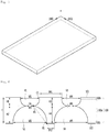
- FIGS. 3 and 4 are views illustrating a front view of a metal plate 100.
- the metal plate 100 may include a plurality of through-holes.
- the plurality of through-holes shown in FIG. 3 may represent the second surface hole V2.
- deviation of the diameter Cx in the horizontal direction and the diameter Cy in the vertical direction between holes (six holes in total as shown in the drawing) adjacent to the reference hole may be implemented at 2% to 10%, respectively. That is, when a size deviation between adjacent holes of one reference hole is implemented at 2% to 10%, uniformity of the deposition may be ensured.
- the size deviation between the reference hole and the adjacent holes may be 4% to 9%.
- the size deviation between the reference hole and the adjacent holes may be 5% to 7%.
- an occurrence rate of moire in an OLED panel after deposition may be increased.
- an occurrence rate of color stain in the OLED panel after deposition may be increased.
- An embodiment may be implemented at a size deviation within ⁇ 3 ⁇ m between the reference hole and the adjacent holes. Accordingly, deposition efficiency may be improved.
- the through-holes may be disposed in a row in a vertical axis and in a row in a horizontal axis.
- the through-holes may be disposed in a row in the vertical axis and may be disposed to be staggered from each other in the horizontal axis.
- the through-hole may have a first diameter measured in the vertical direction and a second diameter measured in the horizontal direction, which may correspond to each other or may be different from each other.
- the through-hole may have a third diameter measured in a first diagonal direction corresponding to a cross-sectional direction of A-A'and a fourth diameter measured in a second diagonal direction intersecting the first diagonal direction, which may be correspond to each other or may be different from each other.
- the through-hole may be rounded.
- FIG. 5 is a view illustrating a relationship between a crystal plane orientation and a rolling direction of a metal plate.
- the polycrystal may represent a crystal texture having a preferred orientation by manufacturing processes such as rolling, annealing, heat treatment, and the like.
- the metal plate 100 includes invar including about 35 to 37 wt% of nickel, about 63 to 65 wt% of iron, and at least one of a trace amount of C, Si, S, P, Cr, Mo, Mn, Ti, Co, Cu, Fe, Ag, Nb, V, In, and Sb.
- the trace amount may refer to less than or equal to 1 wt%.
- the trace amount may refer to less than or equal to 0.5 wt%. Since a nickel alloy such as the invar has a small thermal expansion coefficient, it has advantage that a lifetime of the mask for deposition may be increased. However, it has a problem that uniform etching for the nickel alloy such as the invar is difficult.
- the through-hole may be enlarged to a side surface as the etch rate increases in an initial stage of the etching, and thus de-filming of a photoresist layer may occur.
- the invar is etched, it may be difficult to form a through-hole having a fine size as a size of the through-hole increases. Further, the through-hole is formed non-uniformly, so that a yield of the mask for deposition may be deteriorated.
- the metal plate used in the manufacturing of the mask for deposition according to first and second embodiments includes : an outer layer defined by a thickness range of less than or equal to 1 ⁇ m from a surface of the metal plate; and an inner layer other than the outer layer, wherein an etch rate of the outer layer is slower than that of the inner layer.
- the first embodiment is firstly directed to reducing the etch rate at a surface of the metal plate 100.
- the invar of face centered cubic may have a cubic texture re-crystallized by rolling, heat treatment and the like.
- a re-crystal texture may be oriented in the rolling direction, that is, may be ⁇ 100 ⁇ oriented in a longitudinal direction of the metal plate.
- the metal plate 100 includes two or more crystal planes having different orientations from each other.
- a rolled surface may include ⁇ 111 ⁇ , ⁇ 200 ⁇ and ⁇ 220 ⁇ crystal planes. That is, the surface of the metal plate 100 may include ⁇ 111 ⁇ , ⁇ 200 ⁇ and ⁇ 220 ⁇ crystal planes.
- the etch rate at the first surface 101 and the second surface 102 of the metal plate 100 may be reduced. That is, an embodiment may reduce the etch rate in the initial stage of the etching, prevent the photoresist layer from being de-filmed or separated, and improve uniformity of the through-hole. In addition, fine through-holes may be formed, and a manufacturing yield of the through-holes and process efficiency may be improved.
- the first embodiment in the etching process is secondarily directed that an etching factor of a surface hole is more than or equal to 2.0.
- the etching factor of the surface hole is more than or equal to 2.0, the etching characteristics may be excellent, and uniform and fine-sized through-holes may be formed.
- the first embodiment is thirdly directed to increasing etching uniformity at a surface of the metal plate 100.
- the metal plate 100 according to the first embodiment may include a grain boundary, which has an average size of less than or equal to 30 ⁇ m.
- the rolled metal plate may include a grain boundary, which has an average size of less than or equal to 30 ⁇ m .
- the metal plate 100 may include a grain boundary.
- the grain boundary may have a higher etch rate than a crystal grain. That is, the metal plate 100 according to an embodiment includes a grain boundary having an average size of less than or equal to 30 ⁇ m, thereby increasing uniformity of the etching. Accordingly, a shape of the through-hole may be uniform, and surface roughness of the through-hole may be low.
- an inner circumferential surface of the through-hole may be a smooth curved line, and uniformity of a pattern shape to be deposited via the same may be improved.
- the etching may occur along the grain boundary, so that the etching shape may be irregular and the surface roughness of the through-hole may be large.
- the etching shape is non-uniform at the initial stage of the etching, corrosion may proceed in a gap of a non-uniform shape, and the uniformity of the through-hole may be deteriorated. Therefore, uniformity of the pattern shape deposited via the same may be deteriorated.
- the metal plate 100 may be ASTM E112 standard, and the number of crystal grains may be 7 to 13.
- the metal plate 100 may be ASTM E112 standard, and the number of crystal grains may be 7 to 12.
- the metal plate 100 may be ASTM E112 standard, and the number of crystal grains may be 8 to 11.
- the metal plate according to the first embodiment is ASTM E112 standard
- the metal plate may include 7 to 13 crystal grains, and thus the etching characteristics may be excellent, and a through-hole whose inner circumferential surface is smooth may be formed.
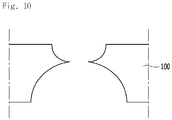
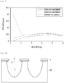
- FIG. 6 is a view of a first embodiment in which a cross section of a plurality of through-holes is enlarged.
- the metal plate 100 used for manufacturing the mask for deposition includes an inner layer 100a and outer layers 100b and 100c.
- the metal plate 100 includes outer layers 100b and 100c defined by the thickness range of less than or equal to 1 ⁇ m from the surface of the metal plate, and an inner layer 100a other than the outer layers.
- the metal plate 100 includes a first outer layer 100b defined by a thickness range of less than or equal to 1 ⁇ m from the first surface 101 of the metal plate and a second outer layer 100c defined by a thickness range of less than or equal to 1 ⁇ m from the second surface 102 of the metal plate.
- the metal plate 100 may include a first outer layer 100b defined by a thickness range of less than or equal to 0.5 ⁇ m from the first surface 101 of the metal plate and a second outer layer 100c defined by a thickness range of less than or equal to 0.5 ⁇ m from the second surface 102 of the metal plate.
- the metal plate 100 may include a first outer layer 100b defined by a thickness range of less than or equal to 0.1 ⁇ m from the first surface 101 of the metal plate and a second outer layer 100c defined by a thickness range of less than or equal to 0.1 ⁇ m from the second surface 102 of the metal plate.
- first outer layer 100b defined by a thickness range of less than or equal to 0.1 ⁇ m from the first surface 101 of the metal plate
- a second outer layer 100c defined by a thickness range of less than or equal to 0.1 ⁇ m from the second surface 102 of the metal plate.
- embodiments are not limited thereto, and may have various thicknesses. That is, the ⁇ 220 ⁇ crystal plane of the outer layer may obviously have various thicknesses within a range of an alloy manufactured to include more than or equal to the ⁇ 220 ⁇ crystal plane of the inner layer.
- a thickness of the inner layer 100a may be greater than that of the outer layer.
- the thickness of the inner layer 100a may be greater than that of the first outer layer 100b and that of the second outer layer 100c.
- a thickness T of the metal plate 100 may be 10 to 50 ⁇ m.
- the thickness T of the metal plate 100 may be 10 to 30 ⁇ m.
- manufacturing efficiency may be low.
- the thickness T of the metal plate 100 is in the range of 10 to 30 ⁇ m to manufacture the mask for deposition, deposition efficiency may be improved.
- the thickness T of the metal plate 100 is more than 50 ⁇ m, process efficiency for forming the through-holes may be deteriorated.
- the thickness T of the metal plate 100 may be measured after the rolling process.
- the thickness of the inner layer 100a may be less than or equal to 50 ⁇ m.
- the thickness of the inner layer 100a may be less than or equal to 30 ⁇ m.
- the first outer layer 100b and the second outer layer 100c may have a thickness corresponding to each other.
- the "corresponding" may include an error due to tolerance.
- the inner layer 100a, the first outer layer 100b, and the second outer layer 100c includes invar.
- the inner layer 100a has a different ratio of a crystal plane included in the inner layer 100a from that of the outer layers 100b and 100c.
- the ratio of the ⁇ 220 ⁇ crystal plane of the metal plate is greater in the outer layers 100b and 100c than the inner layer 100a.
- the metal plate 100 is controlled such that the ratio of the ⁇ 220 ⁇ crystal plane of the outer layers 100b and 100c is higher than that of the inner layer 100a so that the etch rate in the outer layers 100b and 100c is slower than that of the inner layer 100a. Accordingly, the metal plate 100 according to the first embodiment may have excellent etching characteristics in a thickness direction of the metal plate, that is, in a depth direction of the through-holes, and thus the etching factor may be increased. That is, the metal plate 100 may be controlled such that the ratio of the ⁇ 220 ⁇ crystal plane of the outer layers 100b and 100c is higher than that of the inner layer 100a, so that the etch rate in the inner layer 100a may be faster than that of the outer layers 100b and 100c. Accordingly, the metal plate 100 according to the first embodiment can have excellent etching characteristics in the thickness direction of the metal plate, that is, in the depth direction of the through-holes, and the etching factor can be increased.
- the first embodiment may manufacture the mask for deposition which has an excellent etching characteristic and in which etching uniformity of the through-hole is improved.
- the ratio of diffraction intensity of X-rays of the inner layer 100a and that of the outer layers 100b and 100c may be different from each other.
- the ratio of diffraction intensity of X-rays of the ⁇ 220 ⁇ crystal plane of the metal plate may be larger in the outer layers 100b and 100c than in the inner layer 100a. Accordingly, it can be seen that the outer layers 100b and 100c have a higher ratio of the ⁇ 220 ⁇ crystal plane than the inner layer 100a.
- the ratio of the ⁇ 220 ⁇ crystal plane of the metal plate 100 may decrease from the surface as toward the thickness direction of the metal plate. Specifically, in the metal plate 100 according to the embodiment, the ratio of the ⁇ 220 ⁇ crystal plane is reduced from the first surface 101 and the second surface 102 to a region between the first surface 101 and the second surface 102, that is, in a middle region having a half thickness of the metal plate 100.
- the metal plate 100 may have different widths of through-holes along the thickness direction of the through-hole.
- a width W1 of the first surface hole V1 may be greater than a width W3 of the connecting part CA.
- the width of the through-hole may be reduced as the first surface hole V1 goes from the first surface 101 toward the connecting part CA. More specifically, the width of the through-hole may be gradually reduced as the first surface hole V1 goes from the first surface 101 toward the connecting part CA.
- a width W2 of the second surface hole V2 may be greater than the width W3 of the connecting part CA.
- the width of the through-hole may be reduced as the second surface hole V2 goes from the second surface 102 toward the connecting part CA. More specifically, the width of the through-hole may be gradually reduced as the second surface hole V2 goes from the second surface 102 toward the connecting part CA.
- the width of the through-hole may be more than or equal to 20 ⁇ m.
- the width of the through-hole may be 20 to 40 ⁇ m.
- at least one of the width W1 of the first surface hole and the width W2 of the second surface hole may have a width of more than or equal to 20 ⁇ m.
- at least one of the width W1 of the first surface hole and the width W2 of the second surface hole may have a width of 20 to 40 ⁇ m.
- a height H2 of the second surface hole V2 may be greater than a height H1 of the first surface hole V1.
- the height H1 of the first surface hole V1 may have a ratio of 1:3 to 30 to the thickness T of the metal plate 100.
- the height H1 of the first surface hole V1 may have a ratio of 1:3.5 to 12.5 with respect to the thickness T of the metal plate 100.
- the height H1 of the first surface hole V1 may have a ratio of 1:4.5 to 10.5 in relation to the thickness T of the metal plate 100.
- the height H1 of the first surface hole V1 is more than the ratio in relation to the thickness T of the metal plate 100, the height H1 of the first surface hole V1 is increased and the thickness variation of an organic material is increased and thus, a region in which an organic material is not deposited may occur. Accordingly, a manufacturing yield of the OLED panel manufactured through the mask for deposition may be reduced.
- the height H1 of the first surface hole V1 may be 0.1 to 7 ⁇ m.
- the height H1 of the first surface hole V1 may be 1 to 6 ⁇ m.
- the height H1 of the first surface hole V1 may be 2 to 4.5 ⁇ m.
- the height H1 of the first surface hole V1 is less than 0.1 ⁇ m, deposition efficiency of the organic material via the metal plate may be reduced.
- the height H1 of the first surface hole V1 is more than 7 ⁇ m, it is difficult to form a pattern of a fine size and a region in which an organic material is not deposited may occur, and thus the yield of the OLED panel manufactured through the same may be deteriorated.
- a third surface hole V3 adjacent to the first surface hole V1 and formed on the first surface 101 communicates with a fourth surface hole V4 adjacent to the second surface hole V2 and formed on the second surface 102, through the connecting part CA respectively, a plurality of through-holes may be formed.
- the metal plate may include a bridge region BR between an arbitrary first through-hole and a second through-hole adjacent to the first through-hole.
- the first surface 101 between the first surface hole V1 and the third surface hole V3 may include a first bridge region BR1
- the second surface 102 between the second surface hole V2 and the fourth surface hole V4 may include a second bridge region BR2.
- An inclination angle connecting an arbitrary point A1 of an end of the connecting part CA to an arbitrary point B1 of an end of the second surface hole V2 may be in the range of 20 to 70 degrees.
- the inclination angle connecting an arbitrary point A1 of an end of the connecting part CA to an arbitrary point B1 of an end of the second surface hole V2 may be in the range of 30 to 60 degrees.
- the inclination angle connecting an arbitrary point A1 of an end of the connecting part CA to an arbitrary point B1 of an end of the second surface hole V2 may be in the range of 32 to 38 degrees or 52 to 58 degrees.
- the inclination angle connecting an arbitrary point A1 of an end of the connecting part CA to an arbitrary point B1 of an end of the second surface hole V2 is in the range of 20 to 70 degrees, uniformity of the deposition may be improved.
- the inclination angle is out of the range, a region in which an organic material is not deposited may occur, and thus deposition efficiency and process efficiency may be deteriorated.
- the width of the through-hole may become narrower as the first surface hole V1 goes toward a center of the metal plate 100.
- an inner surface of the first surface hole V1 may be a structure having curvature.
- the width of the through-hole may become narrower as the second surface hole V2 goes toward the center of the metal plate 100.
- the inner surface of the first surface hole V1 may be a structure having curvature. Accordingly, an introduction density of the deposition material may be controlled, and uniformity of the deposition may be improved as compared with a simple slope structure.
- a difference W1-W3 between the width W1 of the first surface hole V1 and the width W3 of the connecting part CA may be in the range of 0.2 to 14 ⁇ m.
- a vertical distance from an arbitrary point C1 at an end of the first surface hole V1 to an arbitrary point A1 at an end of the connecting part CA may be in the range of 0.1 to 7 ⁇ m.
- the vertical distance from an arbitrary point C1 at an end of the first surface hole V1 to an arbitrary point A1 at an end of the connecting part CA may be in the range of 1 to 6 ⁇ m.
- the vertical distance from an arbitrary point C1 at an end of the first surface hole V1 to an arbitrary point A1 at an end of the connecting part CA may be in the range of 2 to 4.5 ⁇ m.
- the vertical distance is less than 0.1 ⁇ m, deposition efficiency of the organic material via the metal plate 100 may be reduced.
- the vertical distance is more than 7 ⁇ m, it is difficult to form a pattern of a fine size and a region in which an organic material is not deposited may occur, and thus the yield of the OLED panel manufactured through the same may be deteriorated.
- the first surface hole V1 may have a curvature at an edge portion of an open region on the first surface 101, that is, an outer portion of an open region.
- the second surface hole V2 may have a curvature at an edge portion of an open region on the second surface 102, that is, an outer portion of an open region.
- the edge portion of the open region may be a rounded structure having curvature of a predetermined range.
- a diameter of a virtual circle formed by extending the curvature of the rounded portion of the edge portion may be in the range of 5 to 20 ⁇ m.
- the diameter of a virtual circle formed by extending the curvature of the rounded portion of the edge portion may be in the range of 7 to 15 ⁇ m.
- the diameter of a virtual circle formed by extending the curvature of the rounded portion of the edge portion may be in the range of 8 to 12 ⁇ m. In the range, the deposition rate is high and an organic material may be deposited uniformly.
- a width W5 of the fourth surface hole V4 may be greater than a width W4 of the third surface hole V3.
- the width W4 of the third surface hole V3 may be greater than a width W6 of the connecting part CA.
- the width of the through-hole may be reduced as the third surface hole V3 goes from the first surface 101 toward the connecting part CA.
- the width of the through-hole may be gradually reduced as the third surface hole V3 goes from the first surface 101 toward the connecting part CA.
- the width W5 of the fourth surface hole V4 may be greater than the width W6 of the connecting part CA.
- the width of the through-hole may be reduced as the fourth surface hole V4 goes from the second surface 102 toward the connecting part CA.
- the width of the through-hole may be gradually reduced as the fourth surface hole V4 goes from the second surface 102 toward the connecting part CA.
- a height H4 of the fourth surface hole V4 may be greater than a height H3 of the third surface hole V3.
- the etch rate of the first outer layer 100b is slower than that of the inner layer 100a.
- the etch rate of the second outer layer 100c is slower than that of the inner layer 100a.
- the width of the through-hole formed at the surface of the metal plate 100 may be increased. Accordingly, it is difficult to form a through-hole having a fine pattern, and a manufacturing yield may be deteriorated. In addition, uniformity of a plurality of through-holes may be deteriorated. Therefore, the OLED panel manufactured through the same may have low deposition efficiency of the pattern, and uniformity of the deposition of the pattern may be deteriorated.
- the width W1 of the first surface hole V1 may correspond to the width W4 of the third surface hole V3 and the width W2 of the second surface hole V2 may correspond to the width W5 of the fourth surface hole V4.
- the height H1 of the first surface hole V1 may correspond to the height H3 of the third surface hole V3 and the height H2 of the second surface hole V2 may correspond to the height H4 of the fourth surface hole V4.
- the uniformity of the width and height of the plurality of through-holes may be improved.
- the metal plate according to the first embodiment may be formed such that the etch rate of the outer layers 100b and 100c is slower than that of the inner layer so that the through-hole may have a small width and a deep thickness. Accordingly, it possible to prevent a de-filming phenomenon of the photoresist layer from being caused by a rapid etching at a metal surface. Therefore, the mask for deposition according to the first embodiment may form the plurality of through-holes having uniformity, and process efficiency of manufacturing the mask for deposition may be improved.
- the metal plate used for manufacturing the mask for deposition according to the first embodiment may control the etch rate at the surface, and may manufacture a through-hole having a fine pattern. Further, a manufacturing yield of the metal plate used for manufacturing the mask for deposition may be improved, and uniformity of the plurality of through-holes may be improved. Accordingly, the OLED panel manufactured by using such a mask for deposition has excellent deposition efficiency of the pattern and may improve deposition uniformity.
- the metal plate 100 used for manufacturing the mask for deposition according to the first embodiment may have different etch rates of the inner layer 100a and the outer layers 100b and 100c.
- the etch rate of the outer layers 100b and 100c may be less than or equal to 0.03 ⁇ m/sec.
- the etch rate of the outer layers 100b and 100c may be less than or equal to 0.01 to 0.03 ⁇ m/sec.
- the etch rate of the outer layers 100b and 100c may be less than or equal to 0.02 to 0.03 ⁇ m/sec.
- the etch rate of the outer layers 100b and 100c may be less than or equal to 0.01 to 0.02 ⁇ m/sec.
- the etch rate of the inner layer 100a may be 0.03 to 0.06 ⁇ m/ sec.
- the etch rate of the inner layer 100a may be 0.03 to 0.05 ⁇ m/sec.
- the metal plate used for manufacturing the mask for deposition according to an embodiment may have an etch rate of the outer layers 100b and 100c which is slower than an etch rate of the inner layer 100a, so that the etching characteristics of the through-holes may be excellent.
- the OLED panel manufactured by using the mask for deposition according to an embodiment has excellent deposition efficiency of the pattern and may improve deposition uniformity.
- a manufacturing method of a mask for deposition according to the first embodiment may include: preparing a base metal plate; rolling the base metal plate; forming a photoresist layer on a first surface of the base metal plate and disposing a second photoresist layer on a second surface; and etching to form a through-hole through which a first surface hole of the first surface and a second surface hole of the second surface communicate with each other.
- the mask for deposition including a plurality of through-holes may be manufactured by removing the photoresist layer.
- a nickel alloy is prepared in the base metal plate.
- the base metal plate is invar including about 35 to 37 wt% of nickel, about 63 to 65 wt% of iron, and at least one of a trace amount of C, Si, S, P, Cr, Mo, Mn, Ti, Co, Cu, Fe, Ag, Nb, V, In, and Sb.
- the rolled base metal plate 100 may have a thickness T1 of less than or equal to 50 ⁇ m.
- the base metal plate 100 has different crystal planes of an outer layer corresponding to a thickness range of less than or equal to 1 ⁇ m from the surface of the base metal plate and inner layers other than the outer layer by rolling.
- the ratio of the ⁇ 220 ⁇ crystal plane of the outer layer is greater than that of the ⁇ 220 ⁇ crystal plane of the inner layer.
- a first photoresist layer P1 may be disposed on the first surface 101 of the base metal plate and a second photoresist layer P2 may be formed on the second surface 102 of the base metal plate.
- a photoresist material may be coated on the first surface 101 and the second surface 102 of the base metal plate, respectively and the first photoresist layer P1 and the second photoresist layer P2 may be disposed by an exposure and development process, respectively.
- the first photoresist layer P1 and the second photoresist layer P2 are disposed such that widths of open regions are different from each other, so that the width of the first surface hole V1 formed on the first surface 101 and the width of the second surface hole V2 formed on the second surface 102 may be different.
- the etching process may be performed by a wet etching process.
- the first surface 101 and the second surface 102 may be simultaneously etched.
- the wet etching process may be performed at about 45 °C by using an etchant containing iron chloride.
- the etchant may contain 35 to 45 wt% of FeCl 3 .
- the etchant may contain 36 wt% of FeCl 3 .
- specific gravity of the etchant containing 43 wt% of FeCl 3 may be 1.47 at 20 °C.
- the specific gravity of the etchant containing 41 wt% of FeCl 3 may be 1.44 at 20 °C.
- the specific gravity of the etchant containing 38 wt% of FeCl 3 may be 1.39 at 20 °C.
- an etching factor of at least one of the first and second surface holes calculated by Equation 1 may be more than or equal to 2.0.
- EtchingFactor 2 C B ⁇ A
- the B may be a width of an etched surface hole
- the A may be a width of an opened photoresist layer
- the C may refer to a depth of the etched surface hole.
- the etching factor becomes larger, it may mean that the etching characteristics are excellent in the thickness direction of the metal plate, that is, the depth direction of the through-hole.
- the etching factor becomes smaller, it means that the width of the through-hole is larger. That is, since the width of the through-hole increases as the etching factor becomes smaller, a phenomenon that the photoresist layer is lifted or separated may occur.
- the metal plate having a plurality of through-holes may be formed by removing the first photoresist layer P1 and the second photoresist layer P2.
- an outer layer of the invar metal was formed such that the ratio of the ⁇ 220 ⁇ crystal plane was greater than that of an inner layer other than the outer layer.
- the diffraction intensity of X-rays was measured at the outer layer in a thickness range of less than or equal to 1 ⁇ m from a surface of the invar metal, was measured at the inner layer located at a region of a depth of 10 ⁇ m from the surface of the invar metal, and was measured at the inner layer located at a region of a depth of 15 ⁇ m from the surface of the invar metal.
- an outer layer of the invar metal was formed such that the ratio of the ⁇ 220 ⁇ crystal plane was smaller than that of an inner layer other than the outer layer.
- invar metal and the diffraction intensity of X-rays were the same as those of Exemplary Embodiment 1, except that rolling conditions were different.
- the ratio of the crystal plane disposed on the surface of the metal plate is indicated by measurement of the diffraction intensity of X-rays.
- the diffraction intensity of X-rays of the ⁇ 220 ⁇ crystal plane of the outer layer of Exemplary Embodiment 1 may be greater than that of the ⁇ 220 ⁇ crystal plane of the inner layer located at a region of the depth of 10 ⁇ m from the surface of the invar metal. Specifically, the diffraction intensity of X-rays of the ⁇ 220 ⁇ crystal plane of the outer layer of Exemplary Embodiment 1 may be at least two times greater than that of the ⁇ 220 ⁇ crystal plane of the inner layer located at a region of the depth of 10 ⁇ m from the surface of the invar metal.
- the diffraction intensity of X-rays of the ⁇ 220 ⁇ crystal plane of the outer layer of Exemplary Embodiment 1 may be at least 2.1 times greater than that of the ⁇ 220 ⁇ crystal plane of the inner layer located at a region of the depth of 10 ⁇ m from the surface of the invar metal. Accordingly, it can be seen that the ratio of the ⁇ 220 ⁇ crystal plane of the outer layer of Exemplary Embodiment 1 is greater than that of the ⁇ 220 ⁇ crystal plane of the inner layer located at a region of the depth of 10 ⁇ m from the surface of the invar metal.
- the diffraction intensity of X-rays of the ⁇ 220 ⁇ crystal plane of the outer layer of Exemplary Embodiment 1 is greater than that of the ⁇ 220 ⁇ crystal plane of the inner layer located at a region of the depth of 15 ⁇ m from the surface of the invar metal.
- the diffraction intensity of X-rays of the ⁇ 220 ⁇ crystal plane of the outer layer of Exemplary Embodiment 1 may be at least two times greater than that of the ⁇ 220 ⁇ crystal plane of the inner layer located at a region of the depth of 15 ⁇ m from the surface of the invar metal.
- the diffraction intensity of X-rays of the ⁇ 220 ⁇ crystal plane of the outer layer of Exemplary Embodiment 1 may be at least 2.2 times greater than that of the ⁇ 220 ⁇ crystal plane of the inner layer located at a region of the depth of 15 ⁇ m from the surface of the invar metal. Accordingly, it can be seen that the ratio of the ⁇ 220 ⁇ crystal plane of the outer layer of Exemplary Embodiment 1 is greater than that of the ⁇ 220 ⁇ crystal plane of the inner layer located at a region of the depth of 15 ⁇ m from the surface of the invar metal.
- the diffraction intensity of X-rays of the ⁇ 220 ⁇ crystal plane of the inner layer located at a region of the depth of 10 ⁇ m from the surface of the invar metal of Exemplary Embodiment 1 is greater than that of the ⁇ 220 ⁇ crystal plane of the inner layer located at a region of the depth of 15 ⁇ m from the surface of the invar metal.
- the diffraction intensity of X-rays of the ⁇ 220 ⁇ crystal plane of the inner layer located at a region of the depth of 10 ⁇ m from the surface of the invar metal of Exemplary Embodiment 1 may be at least 1.1 times greater than that of the ⁇ 220 ⁇ crystal plane of the inner layer located at a region of the depth of 15 ⁇ m from the surface of the invar metal.
- the ratio of the ⁇ 220 ⁇ crystal plane of the inner layer located at a region of the depth of 10 ⁇ m from the surface of the invar metal of Exemplary Embodiment 1 is greater than that of the ⁇ 220 ⁇ crystal plane of the inner layer located at a region of the depth of 15 ⁇ m from the surface of the invar metal.
- the ratio of the ⁇ 220 ⁇ crystal plane of Exemplary Embodiment 1 may decrease from the outer layer as toward a center of the inner layer.
- the ratio of the ⁇ 220 ⁇ crystal texture of the outer layer to the ratio of the ⁇ 220 ⁇ crystal texture of the inner layer of Exemplary Embodiment 1 is more than 1 (The ratio of the ⁇ 220 ⁇ crystal texture of the outer layer / the ratio of the ⁇ 220 ⁇ crystal texture of the inner layer > 1). Accordingly, in Exemplary Embodiment 1, the etch rate in the outer layer may be reduced compared with that in the inner layer, and thus the etching factor may be improved.
- the etching characteristics may be excellent in a thickness direction of the metal plate, that is, a depth direction of the through-hole, and thus the through-hole having a fine size may be formed to have excellent uniformity.
- the ratio of the ⁇ 220 ⁇ crystal plane of the outer layer according to Exemplary Embodiment 1 may be greater than that of a ⁇ 111 ⁇ crystal plane of the outer layer.
- the ratio of the ⁇ 220 ⁇ crystal plane of the outer layer according to Exemplary Embodiment 1 is greater than that of a ⁇ 200 ⁇ crystal plane of the outer layer.
- the ratio of the diffraction intensity of X-rays of the ⁇ 220 ⁇ crystal plane to the ratio of the diffraction intensity of X-rays of the ⁇ 200 ⁇ crystal plane of the metal plate, measured in the outer layer according to Exemplary Embodiment 1 is more than 1 ( ⁇ 220 ⁇ X-ray intensity ratio / ⁇ 200 ⁇ X-ray intensity ratio> 1).
- the ratio of the ⁇ 220 ⁇ crystal plane of the inner layer measured at an inside of 10 ⁇ m from a surface of the metal plate according to Exemplary Embodiment 1 may be greater than the ratio of the ⁇ 111 ⁇ crystal plane of the inner layer measured at an inside of 10 ⁇ m from the surface of the metal plate. Further, the ratio of the ⁇ 220 ⁇ crystal plane of the inner layer measured at an inside of 10 ⁇ m from the surface of the metal plate according to Exemplary Embodiment 1 may be greater than the ratio of the ⁇ 200 ⁇ crystal plane of the inner layer measured at an inside of 10 ⁇ m from the surface of the metal plate.
- the ratio of the diffraction intensity of X-rays of the ⁇ 220 ⁇ crystal plane to the ratio of the diffraction intensity of X-rays of the ⁇ 200 ⁇ crystal plane, measured at the inside of 10 ⁇ m from the surface of the metal plate according to Exemplary Embodiment 1 is more than 1 ( ⁇ 220 ⁇ X-ray intensity ratio / ⁇ 200 ⁇ X-ray intensity ratio> 1).
- the diffraction intensity of X-rays of the ⁇ 220 ⁇ crystal plane of the outer layer of Comparative Example 1 may be smaller than that of the ⁇ 220 ⁇ crystal plane of the inner layer located at a region of the depth of 10 ⁇ m from the surface of the invar metal. Specifically, the diffraction intensity of X-rays of the ⁇ 220 ⁇ crystal plane of the inner layer located at a region of the depth of 10 ⁇ m from the surface of the invar metal of Comparative Example 1 may be at least 2 times greater than that of the ⁇ 220 ⁇ crystal plane of the outer layer.
- the diffraction intensity of X-rays of the ⁇ 220 ⁇ crystal plane of the inner layer located at a region of the depth of 10 ⁇ m from the surface of the invar metal of Comparative Example 1 may be at least 2.5 times greater than that of the ⁇ 220 ⁇ crystal plane of the outer layer. Accordingly, it can be seen that the ratio of the ⁇ 220 ⁇ crystal plane of the outer layer of Comparative Example 1 is smaller than that of the ⁇ 220 ⁇ crystal plane of the inner layer located at a region of the depth of 10 ⁇ m from the surface of the invar metal.
- the diffraction intensity of X-rays of the ⁇ 220 ⁇ crystal plane of the outer layer of Comparative Example 1 may be smaller than that of the ⁇ 220 ⁇ crystal plane of the inner layer located at a region of the depth of 15 ⁇ m from the surface of the invar metal. Specifically, the diffraction intensity of X-rays of the ⁇ 220 ⁇ crystal plane of the inner layer located at a region of the depth of 15 ⁇ m from the surface of the invar metal of Comparative Example 1 may be at least 1.1 times greater than that of the outer layer.
- the diffraction intensity of X-ray of the ⁇ 220 ⁇ crystal plane of the inner layer located at a region of the depth of 15 ⁇ m from the surface of the invar metal of Comparative Example 1 may be at least 1.2 times greater than that of the ⁇ 220 ⁇ crystal plane of the outer layer. Accordingly, it can be seen that the ratio of the ⁇ 220 ⁇ crystal plane of the outer layer of Comparative Example 1 is smaller than that of the ⁇ 220 ⁇ crystal plane of the inner layer located at a region of the depth of 15 ⁇ m from the surface of the invar metal.
- the diffraction intensity of X-rays of the ⁇ 220 ⁇ crystal plane of the inner layer located at a region of the depth of 10 ⁇ m from the surface of the invar metal of Comparative Example 1 may be at least 1.5 times greater than that of the ⁇ 220 ⁇ crystal plane of the inner layer located at a region of the depth of 15 ⁇ m from the surface of the invar metal. Accordingly, it can be seen that the ratio of the ⁇ 220 ⁇ crystal plane of the inner layer located at a region of the depth of 10 ⁇ m from the surface of the invar metal of Comparative Example 1 is greater than that of the ⁇ 220 ⁇ crystal plane of the inner layer located at a region of the depth of 15 ⁇ m from the surface of the invar metal.
- the ratio of the ⁇ 220 ⁇ crystal texture of the outer layer to the ratio of the ⁇ 220 ⁇ crystal texture of the inner layer of Comparative Example 1 may be less than 1 (The ratio of the ⁇ 220 ⁇ crystal texture of the outer layer / the ratio of the ⁇ 220 ⁇ crystal texture of the inner layer ⁇ 1). Accordingly, in Comparative Example 1, the etch rate in the outer layer may be faster compared with that in the inner layer, and thus the etching factor may be low and efficiency of OLED deposition may be deteriorated.
- the ratio of the ⁇ 220 ⁇ crystal plane of the outer layer according to Comparative Example 1 may be smaller than that of the ⁇ 111 ⁇ crystal plane of the outer layer. Further, the ratio of the ⁇ 220 ⁇ crystal plane of the outer layer according to Comparative Example 1 may be smaller than that of the ⁇ 200 ⁇ crystal plane of the outer layer.
- the ratio of the diffraction intensity of X-rays of the ⁇ 220 ⁇ crystal plane of the metal plate to the ratio of the diffraction intensity of X-rays of the ⁇ 200 ⁇ crystal plane thereof, measured in the outer layer according to Comparative Example 1 may be less than 1 ( ⁇ 220 ⁇ X-ray intensity ratio / ⁇ 200 ⁇ X-ray intensity ratio ⁇ 1). Specifically, the ratio of the diffraction intensity of X-rays of the ⁇ 220 ⁇ crystal plane of the metal plate to the ratio of the diffraction intensity of X-rays of the ⁇ 200 ⁇ crystal plane thereof, measured in the outer layer according to Comparative Example 1 may be less than 0.5.
- the ratio of diffraction intensity of X-rays of the ⁇ 220 ⁇ crystal plane of the metal plate to the ratio of the diffraction intensity of X-rays of the ⁇ 200 ⁇ crystal plane thereof, measured in the outer layer according to Comparative Example 1 may be 0.1 to 0.4.
- the ratio of the ⁇ 220 ⁇ crystal plane of the inner layer measured at an inside of 10 ⁇ m from the surface of the metal plate according to Comparative Example 1 may be smaller than the ratio of the ⁇ 200 ⁇ crystal plane of the inner layer measured at an inside of 10 ⁇ m from the surface of the metal plate.
- the ratio of the diffraction intensity of X-rays of the ⁇ 220 ⁇ crystal plane to the ratio of the diffraction intensity of X-rays of the ⁇ 200 ⁇ crystal plane, measured at the inside 10 ⁇ m from the surface according to Comparative Example 1 may be less than 1 ( ⁇ 220 ⁇ X-ray intensity ratio / ⁇ 200 ⁇ X-ray intensity ratio ⁇ 1).
- An opened photoresist layer was formed on each of one surfaces of the rolled invar metal according to Exemplary Embodiment 1 and Comparative Example 1.
- the etching process was proceeded on the surface in which the opened photoresist layer was formed.
- the photoresist layer may include a material capable of maintaining physical/chemical stability in the etching process. Accordingly, the invar metal in which the photoresist layer is disposed may prevent the etching. Meanwhile, as the invar metal located at the open region of the photoresist layer is in contact with the etchant, a surface hole may be formed. One surface hole may be formed at a lower portion of one opened photoresist layer. At this point, the one surface hole may be one of the first surface hole and the second surface hole. A plurality of surface holes may be formed at the lower portions of a plurality of opened photoresist layers simultaneously.
- the etching process was performed at 45 °C by a wet etching process, and the etchant contained 36 wt% of FeCl 3 .
- Table 1 below shows the etching factor and etch rate according to Exemplary Embodiment 1 and Comparative Example 1.
- the etch rate of the outer layer was measured in the thickness range to a point within 1 ⁇ m from the surface of the rolled invar metal plate.
- the etch rate of the inner layer was measured in the range of thickness from the point of 1 ⁇ m to the point of 10 ⁇ m from the surface of the invar metal plate.
- Comparative Example 1 it can be seen that the etch rate of the outer layer is faster than that of the inner layer. That is, in Comparative Example 1, it can be seen that the etch rate at a surface, which has a wide contact area of the etchant, is faster than the etch rate at an inside thereof. Specifically, the etch rate of the outer layer of Comparative Example 1 may be more than 0.03 ⁇ m/sec. More specifically, the etch rate of the outer layer of Comparative Example 1 was measured to be 0.5 ⁇ m/sec.
- the etching factor of the surface hole according to Exemplary Embodiment 1 calculated by Equation 1 may be more than or equal to 2.0.
- the etching factor of the surface hole according to Exemplary Embodiment 1 calculated by Equation 1 may be 2.0 to 2.5.
- the etching factor of the surface hole according to Exemplary Embodiment 1 was measured to be 2.2. Accordingly, uniformity of a plurality of through-holes may be improved.
- the etching factor is more than 2.0, reproducibility of processing may be ensured and a through-hole having a fine size may be formed. Therefore, it is possible to form an OLED pattern of a fine size.
- the etch rate of the inner layer is faster than that of the outer layer.
- the etch rate of the outer layer of Exemplary Embodiment 1 may be less than or equal to 0.03 ⁇ m/sec. More specifically, the etch rate of the outer layer of Exemplary Embodiment 1 was measured to be 0.02 ⁇ m/sec.
- the etch rate of the inner layer according to Exemplary Embodiment 1 may be 0.03 to 0.05 ⁇ m/sec.
- the etch rate of the inner layer of Exemplary Embodiment 1 was measured to be 0.05 ⁇ m/sec.
- the second embodiment is firstly directed to reducing the etch rate at a surface of the metal plate 100.
- the second embodiment may include a surface layer defined by a thickness range of 10 to 30 nm from the surface of the metal plate.
- the surface layer may have a higher oxygen content than a metal layer other than the surface layer. Accordingly, the etch rate on the first and second surfaces of the metal plate may be slow. That is, an second embodiment may reduce the etch rate in the initial stage of the etching, thereby preventing the photoresist layer from being de-filmed or separated. Accordingly, the second embodiment may improve uniformity of through-holes and form a fine through-hole, and thus a manufacturing yield of the through-hole and process efficiency may be improved.
- the second embodiment in the etching process is secondarily directed that an etching factor of a surface hole is more than or equal to 2.0.
- the etching factor of the surface hole is more than or equal to 2.0, the etching characteristics may be excellent, and an uniform through-hole having a fine size may be formed.
- the metal plate 100 used for manufacturing the mask for deposition includes an outer layer defined by the thickness range of less than or equal to 1 ⁇ m from the surface of the metal plate; and an inner layer other than the outer layer.
- the outer layer may include surface layers 110 and 120 defined by the thickness range of 10 to 30 nm from the surface of the metal plate.
- the metal plate according to the second embodiment may include a first surface 101 and a second surface 102 facing the first surface, and the surface layer may include a first surface layer 110 defined by the thickness range of 10 to 30 nm from the first surface 101 and a second surface layer 120 defined by the thickness range of 10 to 30 nm from the second surface 102.
- the metal plate according to the second embodiment may include a surface layer and a base metal plate 100d, which is a metal plate other than the surface layer.
- the metal plate 100 may include the base metal plate 100d, a first surface layer 110 disposed on a first surface 101d of the base metal plate 100d, and a second surface layer 120 disposed on a second surface 102d of the base metal plate 100d facing the first surface 101.
- a thickness of the base metal plate 100d may be greater than that of the surface layer.
- a thickness T1 of the base metal plate 100d may be greater than a thickness T2 of the first surface layer 110 and a thickness T3 of the second surface layer 120.
- the thickness of the metal plate 100 is more than 50 ⁇ m, process efficiency for forming a through-hole may be deteriorated.
- the thickness T1 of the base metal plate 100d may be less than or equal to 50 ⁇ m.
- the thickness T1 of the base metal plate 100d may be less than or equal to 30 ⁇ m.
- the first surface layer 110 and the second surface layer 120 may have a thickness corresponding to each other.
- the "corresponding" may include an error due to tolerance.
- the thickness T2 of the first surface layer 110 may be 10 to 30 nm.
- the thickness T2 of the first surface layer 110 may be 10 to 20 nm.
- the thickness T2 of the first surface layer 110 is less than 10 nm, the effect of lowering the etch rate on the first surface 101 may be reduced, and thus uniformity of the through-hole may be deteriorated.
- the thickness T2 of the first surface layer 110 is less than 10 nm, a through-hole having a large variation in thickness and/or width is formed, so that the pattern formed by the metal plate having the through-hole may not be uniform, and thus manufacturing efficiency of the display device may be deteriorated.
- the thickness T2 of the first surface layer 110 is less than 10 nm, the effect of lowering the etch rate on the first surface 101 may be reduced, and thus it is difficult to form a through-hole having a fine size.
- the thickness T2 of the first surface layer 110 is less than 10 nm, the surface roughness of an inner circumferential surface of the first surface hole V1 increases, so that quality of the deposition pattern formed through the first surface hole V1 may be degraded, and thus process efficiency may be deteriorated.
- the manufacturing efficiency may be deteriorated.
- the thickness T3 of the second surface layer 120 may be 10 to 30 nm.
- the thickness T3 of the second surface layer 120 may be 10 to 20 nm.
- the effect of lowering the etch rate on the second surface 102 may be reduced, and thus uniformity of the through-hole may be deteriorated.
- the thickness T3 of the second surface layer 120 is less than 10 nm, a through-hole having a large variation in thickness and/or width is formed, so that the pattern formed by the metal plate having the through-hole may not be uniform, and thus manufacturing efficiency of the display device may be deteriorated.
- the thickness T3 of the second surface layer 120 is less than 10 nm, the effect of lowering the etch rate on the second surface 102 may be reduced, and thus it is difficult to form a through-hole having a fine size.
- the thickness T3 of the second surface layer 120 is less than 10 nm, the surface roughness of an inner circumferential surface of the second surface hole V2 may be increased.
- the manufacturing efficiency may be deteriorated.
- the base metal plate 100d includes invar including about 35 to 37 wt% of nickel, about 63 to 65 wt% of iron, and at least one of a trace amount of C, Si, S, P, Cr, Mo, Mn, Ti, Co, Cu, Fe, Ag, Nb, V, In, and Sb.
- the base metal plate 100d may have different compositions of elements included in the first surface layer 110. In addition, the base metal plate 100d may have different compositions of elements included in the second surface layer 120.
- the first surface layer 110 and the second surface layer 120 may include an oxygen element.
- the first surface layer 110 and the second surface layer 120 may be metal oxide films. Thicknesses of the first surface layer 110 and the second surface layer 120 may be determined according to a surface treatment time under oxygen-injected sputtering conditions.
- a content of oxygen in the surface layer may be higher than that of oxygen in the outer layer other than the surface layer.
- the content of oxygen in the surface layer may be higher than that of oxygen in the inner layer.
- the content of oxygen in the first surface layer 110 may be higher than that of oxygen in the base metal plate 100d.
- the content of oxygen in the second surface layer 120 may be higher than that of oxygen in the base metal plate 100d.
- the surface layer may be an oxygen layer including oxygen.
- the oxygen layer may have an oxygen content of more than or equal to 1 wt%.
- the oxygen layer may have an oxygen content of more than or equal to 0.1 wt%.
- the oxygen layer may have an oxygen content of more than or equal to 0.01 wt%.
- an embodiment is not limited thereto, and the surface layer may not include oxygen.
- absence of oxygen may mean that oxygen is less than or equal to 0.001 wt%.
- absence of oxygen may mean that oxygen is less than or equal to 0 wt%.
- X-ray photoelectron spectroscopy is used to measure an oxygen content of the first surface layer 110 and the second surface layer 120, which is greater than that of the base metal plate 100d.
- the oxygen content of the first and second surface layers 110 and 120 was measured to be higher than that of the base metal plate 100d via the X-ray photoelectron spectroscopy.
- the high content of oxygen in the first surface layer 110 measured by the X-ray photoelectron spectroscopy was remarkably decreased from the first surface 101d of the base metal plate 100d as a starting point.
- the high content of oxygen in the second surface layer 120 measured by the X-ray photoelectron spectroscopy was remarkably decreased from the second surface 102d of the base metal plate 100d as a starting point.
- the first surface layer 110 and the second surface layer 120 may include at least one of a metal oxide and a metal hydroxide.
- the first surface layer 110 and the second surface layer 120 may include iron oxide and nickel oxide as metal oxides.
- the first surface layer 110 and the second surface layer 120 may include iron hydroxide and nickel hydroxide as metal hydroxides.
- the first surface layer 110 may include at least one of FeO, NiO, FeOH, NiOH, Fe(OH) 2 , Fe(OH) 3 , NiO 2 , NiO 3 , Ni n O m , Fe n O m , Ni n (OH) m and Fe n (OH) m .
- n and m may be integers of more than or equal to 1, respectively, in Ni n O m , Fe n O m , Ni n (OH) m , and Fe n (OH) m .
- the second surface layer 120 may include at least one of FeO, NiO, FeOH, NiOH, Fe(OH) 2 , Fe(OH) 3 , NiO 2 , NiO 3 , Ni n O m , Fe n O m , Ni n (OH) m and Fe n (OH) m .
- n and m may be integers of more than or equal to 1, respectively, in Ni n O m , Fe n O m , Ni n (OH) m , and Fe n (OH) m .
- the etch rate of the first surface layer 110 may be slower than that of the base metal plate 100d.
- the etch rate of the second surface layer 120 may be slower than that of the base metal plate 100d.
- the first surface layer may be disposed on the first surface 101d of the base metal plate 100d and the second surface layer may be disposed on the second surface 102d of the base metal plate 100d, and thus the etch rate at the surface of the metal plate may be reduced.
- the first surface layer 110 and the second surface layer 120 may include an oxygen element so that the etch rate may be slower than that of the base metal plate 100d.
- the first surface layer 110 and the second surface layer 120 are disposed on the base metal plate 100d at a thickness of 10 to 30 nm, respectively, thereby forming a fine through-hole.
- the width W1 of the first surface hole V1 may correspond to the width W4 of the third surface hole V3, and the width W2 of the second surface hole V2 may correspond to the width W5 of the fourth surface hole V4.
- the height H1 of the first surface hole V1 may correspond to the height H3 of the third surface hole V3, and the height H2 of the second surface hole V2 may correspond to the height H4 of the fourth surface hole V4. That is, uniformity of the width and height of the plurality of through-holes may be improved.
- the metal plate according to an embodiment may have a slow etch rate in a region in which the first surface layer 110 and the second surface layer 120 are disposed, so that it is possible to form the through-hole with a small width and a deep thickness. Accordingly, it possible to prevent a de-filming phenomenon of the photoresist layer from being caused by a rapid etching at a metal surface.
- an adhesion force between a ceramic-based surface layer and the photoresist layer may be greater than an adhesion force between the metal layer and the photoresist layer. Accordingly, the metal plate according to an embodiment may improve a manufacturing yield and process efficiency of the plurality of through-holes.
- the inner layer and the outer layer may have different etch rates.
- the etch rate of the outer layer may be less than or equal to 0.03 ⁇ m/sec.
- the etch rate of the outer layer may be less than or equal to 0.01 to 0.03 ⁇ m/sec.
- the etch rate of the outer layer may be less than or equal to 0.02 to 0.03 ⁇ m/sec.
- the etch rate of the inner layer may be 0.03 to 0.06 ⁇ m/sec.
- the etch rate of the inner layer may be 0.03 to 0.05 ⁇ m/sec.
- the metal plate used for manufacturing the mask for deposition according to an embodiment may have an etch rate of the outer layer slower than that of the inner layer, so that the etching characteristics of the through-holes may be excellent.
- the OLED panel manufactured by using the mask for deposition according to an embodiment has excellent deposition efficiency of the pattern and may improve deposition uniformity.
- the width of the through-hole may be more than or equal to 20 ⁇ m.
- the width of the through-hole may be 20 to 40 ⁇ m.
- at least one of the width W1 of the first surface hole and the width W2 of the second surface hole may have a width of more than or equal to 20 ⁇ m.
- at least one of the width W1 of the first surface hole and the width W2 of the second surface hole may have a width of 20 to 40 ⁇ m.
- a manufacturing method of a mask for deposition according to the second embodiment may include: preparing a base metal plate; rolling the base metal plate; forming a surface layer to dispose a first surface layer on a first surface of the base metal plate, and dispose a second surface layer on a second surface of the base metal plate; forming a photoresist layer to dispose a first photoresist layer on the first surface of the base metal plate and dispose a second photoresist layer on a second surface; and etching to form a through-hole through which a first surface hole of the first surface and a second surface hole of the second surface communicate with each other.
- the mask for deposition including a plurality of through-holes may be formed by removing the first and second photoresist layers.
- the base metal plate is invar including about 35 to 37 wt% of nickel, about 63 to 65 wt% of iron, and at least one of a trace amount of C, Si, S, P, Cr, Mo, Mn, Ti, Co, Cu, Fe, Ag, Nb, V, In, and Sb.
- the rolled base metal plate 100d may have a thickness T1 of less than or equal to 50 ⁇ m.
- the rolled base metal plate 100d may have a thickness T1 of less than or equal to 30 ⁇ m.
- a surface layer may be formed on the base metal plate 100d.
- the base metal plate 100d may be heat-treated, so that a surface layer may be formed on the base metal plate 100d.
- the base metal plate 100d may be heat-treated under an oxygen atmosphere, so that the first surface layer 110 may be formed on the first surface 101 d of the base metal plate 100d, and the second surface layer 120 may be formed on the second surface 102d of the base metal plate 100d.
- the first surface layer 110 and the second surface layer 120 may be simultaneously formed by the heat treatment process, thereby improving process efficiency.
- first surface layer 110 and the second surface layer 120 may be disposed on the base metal plate 100d at a thickness corresponding to each other, so that the etch rate of the first surface 101 and the second surface 102 of the base metal plate 100d may be deteriorated.
- the embodiment is not limited thereto, and the surface layer may obviously be formed by anodizing, plasma treatment, or the like.
- a first photoresist layer P1 may be disposed on the first surface 101d of the base metal plate 100d and a second photoresist layer P2 may be formed on the second surface 102d thereof.
- a first photoresist layer P1 may be disposed on the first surface layer 110 and a second photoresist layer P2 may be disposed on the second surface layer 120.
- a photoresist material may be coated on the first surface layer 110 and the second surface layer 120, respectively and the first photoresist layer P1 and the second photoresist layer P2 may be disposed by an exposure and development process, respectively.
- the first photoresist layer P1 and the second photoresist layer P2 are disposed such that widths of open regions are different from each other, so that the width of the first surface hole V1 formed on the first surface 101 and the width of the second surface hole V2 formed on the second surface 102 may be different.
- the etching will be described.
- the first surface hole V1 and the second surface hole V2 may be formed and a through-hole may be formed as the first surface hole V1 and the second surface hole V2 communicate with each other by the connecting part CA.
- the etching process may be performed by a wet etching process.
- the first surface 101 and the second surface 102 may be simultaneously etched.
- the wet etching process may be performed at about 45 °C by using an etchant containing iron chloride.
- the etchant may contain 35 to 45 wt% of FeCl 3 .
- the etchant may contain 36 wt% of FeCl 3 .
- specific gravity of the etchant containing 43 wt% of FeCl 3 may be 1.47 at 20 °C.
- the specific gravity of the etchant containing 41 wt% of FeCl 3 may be 1.44 at 20 °C.
- the specific gravity of the etchant containing 38 wt% of FeCl 3 may be 1.39 at 20 °C.
- the etching factor of at least one of the first and second surface holes calculated by Equation 1 may be more than or equal to 2.0.
- the first photoresist layer P1 and the second photoresist layer P2 may be removed so that a first surface layer 110 and a second surface layer 120 may be disposed on the base metal plate 100d and the metal plate having a plurality of through-holes may be formed.
- a surface layer of 20 nm was formed on rolled invar metal, and then a surface was formed via an etching process.
- the etching process was performed at 45 °C by a wet etching process, and an etchant contained 36 wt% of FeCl 3 .
- a surface layer of 5 nm was formed on rolled invar metal, and then a surface hole was formed by an etching process.
- FIGS. 19 and 20 are photographs of through-holes formed according to Exemplary Embodiment 2 and Comparative Example 2.
- the through-hole formed according to Exemplary Embodiment 2 has a low surface roughness of the through-hole. That is, the inner circumferential surface of the through-hole may be a smooth curved line, and uniformity of the pattern shape deposited through the same may be improved.
- the through-hole formed according to Comparative Example 2 has a large surface roughness of the through-hole. That is, the inner circumferential surface of the through-hole may include a rugged shape, so that the uniformity of the pattern shape deposited through the through-hole may be reduced.
- a surface layer was formed on rolled invar metal.
- the surface layer was formed by heat treatment for a predetermined period of time.
- a surface layer was formed on rolled invar metal.
- the surface layer of exemplary embodiment 3 was formed such that the heat treatment temperature and/or the heat treatment time were different from that of the surface layer of exemplary embodiment 4.
- a thickness of the surface layer of Exemplary Embodiment 4 may be smaller than that of the surface layer of Exemplary Embodiment 3.
- a surface layer was not formed on rolled invar metal, and a surface hole was formed by an etching process.
- the metal surfaces of Exemplary Embodiments 3 and 4 and Comparative Example 3 were measured by XPS analysis.
- XPS was applied at 15 kV, 100 ⁇ m (X-ray beam size), and Ar sputter was measured under the condition of 2 kV 2x2 mm 2 , 10 min.
- the concentration of oxygen was measured in the thickness range of 0 to 100 nm at the metal surface.
- the oxygen concentration of 597.10 was measured in Exemplary Embodiment 3
- the oxygen concentration of 313.75 was measured in Exemplary Embodiment 4
- the oxygen concentration of 233.08 was measured in Comparative Example 3.
- binding energy was 1000 eV
- a counter shot value of oxygen was measured to be more than 3.0X10 4 .
- the oxygen content of the outer layer may be greater than that of the inner layer.
- the oxygen content of the surface layer may be greater than that of the base metal plate, which is the metal plate other than the surface layer.
- the first surface layer 110 and the second surface layer 120 may have a larger oxygen content than a metal content.
- an oxygen content (at%) of the first surface layer 110 and the second surface layer 120 may be greater than an iron content (at%).
- an oxygen content (at%) of the first surface layer 110 and the second surface layer 120 may be greater than a nickel content (at%).
- an oxygen content (at%) of the first surface layer 110 and the second surface layer 120 may be more than or equal to 30 at%.
- an oxygen content (at%) of the first surface layer 110 and the second surface layer 120 may be more than or equal to 50 at%.
- the outer layer of the metal plate according to the second embodiment may include 50% to 70% of the ⁇ 220 ⁇ crystal plane.
- the outer layer of the metal plate according to the second embodiment may include 55% to 70% of the ⁇ 220 ⁇ crystal plane.
- the ⁇ 220 ⁇ crystal plane was measured to be 58.1%, the ⁇ 200 ⁇ crystal plane was 40.8%, and the ⁇ 111 ⁇ crystal plane was 1.0%.
- the inner layer having a thickness range of 10 ⁇ m from a thickness region of 1 ⁇ m of the metal plate of Exemplary Embodiment 3 the ⁇ 220 ⁇ crystal plane was measured to be 24.6%, the ⁇ 200 ⁇ crystal plane was 30.3%, and the ⁇ 111 ⁇ crystal plane was 45.1%.
- the ⁇ 220 ⁇ crystal plane was measured to be 68.9%, the ⁇ 200 ⁇ crystal plane was 28.0%, and the ⁇ 111 ⁇ crystal plane was 3.1%.
- the ⁇ 220 ⁇ crystal plane was measured to be 27.2%, the ⁇ 200 ⁇ crystal plane was 67.3%, and the ⁇ 111 ⁇ crystal plane was 5.5%.
- the inner layer having a thickness range of 10 ⁇ m from a thickness region of 1 ⁇ m of the metal plate of Comparative Example 3 the ⁇ 220 ⁇ crystal plane was measured to be 13.2%, the ⁇ 200 ⁇ crystal plane was 64.8%, and the ⁇ 111 ⁇ crystal plane was 22%.
- the etching factor is deteriorated.
- the ⁇ 220 ⁇ crystal plane included in the outer layer is less than 50%, it can be seen that the etching factor is deteriorated.
- an etching factor and an etch rate in various ranges were measured by changing formation conditions of the surface layer.
- an optimum thickness of the surface layer in which the etching characteristics were improved by changing a heat treatment temperature and a heat treatment time was 10 to 30 nm.
- a metal plate for manufacturing a mask for deposition includes a surface layer of about 5 nm.
- the surface layer was formed at a thickness of 10 to 30 nm.
- etching factor and etch rate in various ranges were measured when a surface hole having a diameter of 20 ⁇ m in a horizontal direction and a diameter of 20 ⁇ m in a vertical direction and a surface hole having a diameter of 25 ⁇ m in the horizontal direction and a diameter of 25 ⁇ m in the vertical direction were formed, respectively.
- the etching factor of the mask for deposition may be 2.0 to 2.9.
- the etching factor of the mask for deposition may be 2.0 to 2.5.
- Table 2 below shows the etching factor and etch rate according to Exemplary Embodiments 3 and 4 and Comparative Example 3.
- the etch rate of the outer layer indicates an etch rate observed at a thickness of less than or equal to 1 ⁇ m from the surface of the metal plate.
- the etch rate of the inner layer indicates an etch rate observed from a thickness of 1 ⁇ m to a thickness of 10 ⁇ m from the surface of the metal plate.
- the etch rate of the outer layer is faster than that of the inner layer.
- the etch rate of the outer layer was measured to be 2 times faster than that of the inner layer. That is, in Comparative Example 3, the etch rate at a surface, which has a wide contact area of the etchant, is faster than the etch rate at an inside thereof.
- the etch rate of the outer layer of Comparative Example 3 may be more than 0.03 um/sec. More specifically, the etch rate of the outer layer of Comparative Example 3 was measured to be 0.1 um/sec.
- the etch rate is maximized within a depth of 10 ⁇ m from the surface of the metal plate.
- the inner layer between 6 and 8 ⁇ m from the surface of the metal plate may have a maximum etch rate.
- the etch rate of the inner layer is faster than that of the outer layer. That is, in Exemplary Embodiments 3 and 4, the surface layer including oxygen element may be disposed on the metal layer, so that the etch rate at the surface of the metal plate may be slower than that in the metal plate. Accordingly, the metal plate according to an embodiment may form a fine through-hole. Specifically, the etch rate of the outer layer of Exemplary Embodiments 3 and 4 may be less than or equal to 0.03 ⁇ m/sec. More specifically, the etch rate of the outer layer of Exemplary Embodiment 3 was measured to be 0.02 ⁇ m/sec, and the etch rate of the outer layer of Exemplary Embodiment 4 was measured to be 0.03 ⁇ m/sec.
- FIG. 22 is a sectional view of a surface hole according to Exemplary Embodiment 3
- FIG. 23 is a sectional view of a surface hole according to Exemplary Embodiment 4.
- Exemplary Embodiments 3 and 4 have a high etching factor of more than or equal to 2.0, so that the width of the through-hole is small and the etching characteristics are excellent in the depth direction. Accordingly, deformation of the photoresist layer may be prevented.
- the pattern capable of being formed through the metal plate according to Exemplary Embodiments 3 and 4 may implement a fine pattern.
- the metal plate may include a base metal plate including first and second surfaces facing each other, a first surface layer disposed on the first surface, and a second surface layer disposed on the second surface, wherein the metal plate may include a plurality of through-holes, the first surface layer and the second surface layer may be opened at a region in which the through-holes are disposed, the first surface layer and the second surface layer may have a thickness of 10 to 30 nm, respectively, a thickness of the metal plate may be less than or equal to 50 um, and the etching factor of at least one of the first surface hole and the second surface hole may be more than or equal to 2.0.
- the surface layer may be disposed on the base metal plate before the through-hole is formed. Accordingly, the surface layer may be opened without being disposed on the region in which the through-hole is disposed.
- the inner region of the through-hole may have a different composition of elements included in the surface layer.
- the content of oxygen in the first surface layer may be higher than that contained in the connecting part of the through-hole.
- the content of oxygen in the second surface layer may be higher than that contained in the connecting part of the through-hole.
- the mask for deposition according to the second embodiment may have a structural feature that the etch rate is gradually increased as it goes from the outer layer toward the inner layer in the etching process for forming the through-holes, and thus etching efficiency and uniformity of the through-hole may be improved.
- the OLED panel manufactured by using the mask for deposition according to an embodiment has excellent deposition efficiency of the pattern and may improve deposition uniformity.
Landscapes
- Chemical & Material Sciences (AREA)
- Engineering & Computer Science (AREA)
- Materials Engineering (AREA)
- Mechanical Engineering (AREA)
- Metallurgy (AREA)
- Organic Chemistry (AREA)
- Chemical Kinetics & Catalysis (AREA)
- General Chemical & Material Sciences (AREA)
- Manufacturing & Machinery (AREA)
- Electroluminescent Light Sources (AREA)
- Physical Vapour Deposition (AREA)
- ing And Chemical Polishing (AREA)
Applications Claiming Priority (3)
| Application Number | Priority Date | Filing Date | Title |
|---|---|---|---|
| KR1020160017682A KR102590890B1 (ko) | 2016-02-16 | 2016-02-16 | 금속판, 증착용마스크 및 이를 이용한 oled 패널 |
| KR1020160040436A KR102556805B1 (ko) | 2016-04-01 | 2016-04-01 | 금속판, 증착용마스크 및 이를 이용한 oled 패널 |
| PCT/KR2017/001043 WO2017142231A1 (ko) | 2016-02-16 | 2017-01-31 | 금속판, 증착용마스크 및 이의 제조방법 |
Publications (3)
| Publication Number | Publication Date |
|---|---|
| EP3419074A1 EP3419074A1 (en) | 2018-12-26 |
| EP3419074A4 EP3419074A4 (en) | 2019-03-20 |
| EP3419074B1 true EP3419074B1 (en) | 2021-04-14 |
Family
ID=59626129
Family Applications (1)
| Application Number | Title | Priority Date | Filing Date |
|---|---|---|---|
| EP17753392.4A Active EP3419074B1 (en) | 2016-02-16 | 2017-01-31 | Metal plate, mask for deposition and manufacturing method therefor |
Country Status (4)
| Country | Link |
|---|---|
| EP (1) | EP3419074B1 (ja) |
| JP (1) | JP7072512B2 (ja) |
| CN (2) | CN108701776B (ja) |
| WO (1) | WO2017142231A1 (ja) |
Families Citing this family (11)
| Publication number | Priority date | Publication date | Assignee | Title |
|---|---|---|---|---|
| KR102375261B1 (ko) * | 2016-04-01 | 2022-03-17 | 엘지이노텍 주식회사 | 증착용마스크 및 이를 이용한 oled 패널 |
| WO2018052197A1 (ko) | 2016-09-13 | 2018-03-22 | 엘지이노텍 주식회사 | 증착 마스크용 금속판, 증착 마스크 및 이의 제조방법 |
| KR20190023652A (ko) * | 2017-08-29 | 2019-03-08 | 엘지이노텍 주식회사 | Oled 화소 증착을 위한 금속재의 증착용 마스크 및 이의 제조방법 |
| CN209210911U (zh) * | 2017-10-13 | 2019-08-06 | 凸版印刷株式会社 | 蒸镀掩模 |
| KR20190055295A (ko) * | 2017-11-14 | 2019-05-23 | 삼성디스플레이 주식회사 | 마스크 제조 장치 및 마스크 제조 방법 |
| KR102479945B1 (ko) * | 2017-12-08 | 2022-12-22 | 삼성디스플레이 주식회사 | 마스크 시트 및 이의 제조 방법 |
| TWI648867B (zh) * | 2018-01-16 | 2019-01-21 | 美屬薩摩亞商茂邦電子有限公司 | Light guide plate with high aspect ratio light guide hole array and manufacturing method thereof |
| JP7481330B2 (ja) | 2018-11-19 | 2024-05-10 | エルジー イノテック カンパニー リミテッド | 合金金属板及びこれを含む蒸着用マスク |
| KR20220090098A (ko) | 2020-12-22 | 2022-06-29 | 엘지이노텍 주식회사 | Oled 화소 증착을 위한 증착용 마스크 |
| US20240055272A1 (en) * | 2020-12-25 | 2024-02-15 | Tokuyama Corporation | Method for processing semiconductor containing transition metal, method for producing semiconductor containing transition metal, and processing liquid for semiconductors |
| TWI828015B (zh) * | 2021-12-01 | 2024-01-01 | 達運精密工業股份有限公司 | 精密金屬遮罩的製造方法 |
Family Cites Families (14)
| Publication number | Priority date | Publication date | Assignee | Title |
|---|---|---|---|---|
| US4303466A (en) * | 1980-06-19 | 1981-12-01 | Buckbee-Mears Company | Process of forming graded aperture masks |
| JPS60200985A (ja) * | 1984-03-26 | 1985-10-11 | Toshiba Corp | シヤドウマスクの製造方法 |
| JPS62247085A (ja) * | 1986-04-17 | 1987-10-28 | Dainippon Screen Mfg Co Ltd | フオトエッチング法による金属薄板の加工方法 |
| US4696098A (en) * | 1986-06-24 | 1987-09-29 | Advanced Micro Devices, Inc. | Metallization technique for integrated circuit structures |
| KR100262007B1 (ko) * | 1998-04-02 | 2000-09-01 | 김영환 | 반도체 장치의 제조 방법 |
| CN1108393C (zh) * | 1999-05-07 | 2003-05-14 | 松下电器产业株式会社 | 荫罩用不锈钢板及其制造方法和荫罩 |
| JP2002220656A (ja) * | 2000-11-22 | 2002-08-09 | Sanyo Electric Co Ltd | 蒸着用マスクおよびその製造方法 |
| JP3775493B2 (ja) * | 2001-09-20 | 2006-05-17 | セイコーエプソン株式会社 | マスクの製造方法 |
| JP2005281836A (ja) * | 2004-03-31 | 2005-10-13 | Jfe Steel Kk | エッチング性に優れたシャドウマスク用Fe−Ni系合金薄板 |
| KR20060134605A (ko) * | 2005-06-23 | 2006-12-28 | 주식회사 하이닉스반도체 | 반도체 소자의 제조방법 |
| CN101517130B (zh) * | 2006-08-07 | 2011-12-28 | 精工电子有限公司 | 电铸模的制造方法、电铸模及电铸部件的制造方法 |
| JP2011034681A (ja) * | 2009-07-29 | 2011-02-17 | Hitachi Displays Ltd | 金属加工方法、金属マスク製造方法及び有機el表示装置製造方法 |
| CN103388121B (zh) * | 2012-05-08 | 2017-07-11 | 昆山允升吉光电科技有限公司 | 一种高精度金属掩模板的混合制作工艺 |
| JP5626491B1 (ja) * | 2014-03-06 | 2014-11-19 | 大日本印刷株式会社 | 金属板、金属板の製造方法、および金属板を用いて蒸着マスクを製造する方法 |
-
2017
- 2017-01-31 EP EP17753392.4A patent/EP3419074B1/en active Active
- 2017-01-31 CN CN201780011646.1A patent/CN108701776B/zh active Active
- 2017-01-31 WO PCT/KR2017/001043 patent/WO2017142231A1/ko active Application Filing
- 2017-01-31 JP JP2018542774A patent/JP7072512B2/ja active Active
- 2017-01-31 CN CN202010848326.5A patent/CN112103403B/zh active Active
Non-Patent Citations (1)
| Title |
|---|
| None * |
Also Published As
| Publication number | Publication date |
|---|---|
| CN112103403A (zh) | 2020-12-18 |
| CN112103403B (zh) | 2023-09-05 |
| EP3419074A1 (en) | 2018-12-26 |
| CN108701776A (zh) | 2018-10-23 |
| CN108701776B (zh) | 2020-09-22 |
| WO2017142231A1 (ko) | 2017-08-24 |
| JP2019507829A (ja) | 2019-03-22 |
| JP7072512B2 (ja) | 2022-05-20 |
| EP3419074A4 (en) | 2019-03-20 |
Similar Documents
| Publication | Publication Date | Title |
|---|---|---|
| EP3419074B1 (en) | Metal plate, mask for deposition and manufacturing method therefor | |
| EP3514844B1 (en) | Metal plate for deposition mask, and deposition mask and manufacturing method therefor | |
| EP3597794B1 (en) | Metal plate, deposition mask, and manufacturing method therefor | |
| CN111066169B (zh) | 用于oled像素沉积的金属材料沉积掩模及其制造方法 | |
| CN109790628A (zh) | 用作沉积掩模的合金金属箔、沉积掩模及其制造方法以及利用该沉积掩模的有机发光元件的制造方法 | |
| KR20170112810A (ko) | 금속판, 증착용마스크 및 이를 이용한 oled 패널 | |
| EP3886195A1 (en) | Alloy metal plate and deposition mask including same | |
| KR20220018532A (ko) | Oled 화소 증착을 위한 금속재의 증착용 마스크 | |
| KR102142752B1 (ko) | 수지 밀착성이 우수한 Fe-Ni계 합금 포일, 그 제조방법, 증착용 마스크 및 상기 증착용 마스크 제조방법 | |
| TW201600459A (zh) | 石墨烯製造方法 |
Legal Events
| Date | Code | Title | Description |
|---|---|---|---|
| STAA | Information on the status of an ep patent application or granted ep patent |
Free format text: STATUS: THE INTERNATIONAL PUBLICATION HAS BEEN MADE |
|
| PUAI | Public reference made under article 153(3) epc to a published international application that has entered the european phase |
Free format text: ORIGINAL CODE: 0009012 |
|
| STAA | Information on the status of an ep patent application or granted ep patent |
Free format text: STATUS: REQUEST FOR EXAMINATION WAS MADE |
|
| 17P | Request for examination filed |
Effective date: 20180810 |
|
| AK | Designated contracting states |
Kind code of ref document: A1 Designated state(s): AL AT BE BG CH CY CZ DE DK EE ES FI FR GB GR HR HU IE IS IT LI LT LU LV MC MK MT NL NO PL PT RO RS SE SI SK SM TR |
|
| AX | Request for extension of the european patent |
Extension state: BA ME |
|
| A4 | Supplementary search report drawn up and despatched |
Effective date: 20190214 |
|
| RIC1 | Information provided on ipc code assigned before grant |
Ipc: H01J 9/14 20060101ALI20190208BHEP Ipc: H01L 51/00 20060101ALI20190208BHEP Ipc: H01L 51/56 20060101AFI20190208BHEP Ipc: C23C 14/04 20060101ALI20190208BHEP Ipc: G03F 7/00 20060101ALI20190208BHEP |
|
| DAV | Request for validation of the european patent (deleted) | ||
| DAX | Request for extension of the european patent (deleted) | ||
| REG | Reference to a national code |
Ref country code: DE Ref legal event code: R079 Ref document number: 602017036706 Country of ref document: DE Free format text: PREVIOUS MAIN CLASS: H01L0051560000 Ipc: C23F0001020000 |
|
| GRAP | Despatch of communication of intention to grant a patent |
Free format text: ORIGINAL CODE: EPIDOSNIGR1 |
|
| STAA | Information on the status of an ep patent application or granted ep patent |
Free format text: STATUS: GRANT OF PATENT IS INTENDED |
|
| RIC1 | Information provided on ipc code assigned before grant |
Ipc: C21D 9/46 20060101ALI20201109BHEP Ipc: C22C 38/08 20060101ALI20201109BHEP Ipc: C21D 8/02 20060101ALI20201109BHEP Ipc: H01L 51/00 20060101ALI20201109BHEP Ipc: C23F 1/02 20060101AFI20201109BHEP Ipc: C23F 1/04 20060101ALI20201109BHEP Ipc: G03F 7/00 20060101ALI20201109BHEP Ipc: C23F 1/28 20060101ALI20201109BHEP Ipc: C21D 6/00 20060101ALI20201109BHEP Ipc: C23C 14/04 20060101ALI20201109BHEP |
|
| INTG | Intention to grant announced |
Effective date: 20201216 |
|
| GRAS | Grant fee paid |
Free format text: ORIGINAL CODE: EPIDOSNIGR3 |
|
| GRAA | (expected) grant |
Free format text: ORIGINAL CODE: 0009210 |
|
| STAA | Information on the status of an ep patent application or granted ep patent |
Free format text: STATUS: THE PATENT HAS BEEN GRANTED |
|
| AK | Designated contracting states |
Kind code of ref document: B1 Designated state(s): AL AT BE BG CH CY CZ DE DK EE ES FI FR GB GR HR HU IE IS IT LI LT LU LV MC MK MT NL NO PL PT RO RS SE SI SK SM TR |
|
| REG | Reference to a national code |
Ref country code: GB Ref legal event code: FG4D |
|
| REG | Reference to a national code |
Ref country code: CH Ref legal event code: EP |
|
| REG | Reference to a national code |
Ref country code: DE Ref legal event code: R096 Ref document number: 602017036706 Country of ref document: DE |
|
| REG | Reference to a national code |
Ref country code: IE Ref legal event code: FG4D |
|
| REG | Reference to a national code |
Ref country code: AT Ref legal event code: REF Ref document number: 1382452 Country of ref document: AT Kind code of ref document: T Effective date: 20210515 |
|
| REG | Reference to a national code |
Ref country code: LT Ref legal event code: MG9D |
|
| REG | Reference to a national code |
Ref country code: AT Ref legal event code: MK05 Ref document number: 1382452 Country of ref document: AT Kind code of ref document: T Effective date: 20210414 |
|
| REG | Reference to a national code |
Ref country code: NL Ref legal event code: MP Effective date: 20210414 |
|
| PG25 | Lapsed in a contracting state [announced via postgrant information from national office to epo] |
Ref country code: FI Free format text: LAPSE BECAUSE OF FAILURE TO SUBMIT A TRANSLATION OF THE DESCRIPTION OR TO PAY THE FEE WITHIN THE PRESCRIBED TIME-LIMIT Effective date: 20210414 Ref country code: LT Free format text: LAPSE BECAUSE OF FAILURE TO SUBMIT A TRANSLATION OF THE DESCRIPTION OR TO PAY THE FEE WITHIN THE PRESCRIBED TIME-LIMIT Effective date: 20210414 Ref country code: NL Free format text: LAPSE BECAUSE OF FAILURE TO SUBMIT A TRANSLATION OF THE DESCRIPTION OR TO PAY THE FEE WITHIN THE PRESCRIBED TIME-LIMIT Effective date: 20210414 Ref country code: HR Free format text: LAPSE BECAUSE OF FAILURE TO SUBMIT A TRANSLATION OF THE DESCRIPTION OR TO PAY THE FEE WITHIN THE PRESCRIBED TIME-LIMIT Effective date: 20210414 Ref country code: AT Free format text: LAPSE BECAUSE OF FAILURE TO SUBMIT A TRANSLATION OF THE DESCRIPTION OR TO PAY THE FEE WITHIN THE PRESCRIBED TIME-LIMIT Effective date: 20210414 Ref country code: BG Free format text: LAPSE BECAUSE OF FAILURE TO SUBMIT A TRANSLATION OF THE DESCRIPTION OR TO PAY THE FEE WITHIN THE PRESCRIBED TIME-LIMIT Effective date: 20210714 |
|
| PG25 | Lapsed in a contracting state [announced via postgrant information from national office to epo] |
Ref country code: IS Free format text: LAPSE BECAUSE OF FAILURE TO SUBMIT A TRANSLATION OF THE DESCRIPTION OR TO PAY THE FEE WITHIN THE PRESCRIBED TIME-LIMIT Effective date: 20210814 Ref country code: GR Free format text: LAPSE BECAUSE OF FAILURE TO SUBMIT A TRANSLATION OF THE DESCRIPTION OR TO PAY THE FEE WITHIN THE PRESCRIBED TIME-LIMIT Effective date: 20210715 Ref country code: NO Free format text: LAPSE BECAUSE OF FAILURE TO SUBMIT A TRANSLATION OF THE DESCRIPTION OR TO PAY THE FEE WITHIN THE PRESCRIBED TIME-LIMIT Effective date: 20210714 Ref country code: LV Free format text: LAPSE BECAUSE OF FAILURE TO SUBMIT A TRANSLATION OF THE DESCRIPTION OR TO PAY THE FEE WITHIN THE PRESCRIBED TIME-LIMIT Effective date: 20210414 Ref country code: PL Free format text: LAPSE BECAUSE OF FAILURE TO SUBMIT A TRANSLATION OF THE DESCRIPTION OR TO PAY THE FEE WITHIN THE PRESCRIBED TIME-LIMIT Effective date: 20210414 Ref country code: PT Free format text: LAPSE BECAUSE OF FAILURE TO SUBMIT A TRANSLATION OF THE DESCRIPTION OR TO PAY THE FEE WITHIN THE PRESCRIBED TIME-LIMIT Effective date: 20210816 Ref country code: SE Free format text: LAPSE BECAUSE OF FAILURE TO SUBMIT A TRANSLATION OF THE DESCRIPTION OR TO PAY THE FEE WITHIN THE PRESCRIBED TIME-LIMIT Effective date: 20210414 Ref country code: RS Free format text: LAPSE BECAUSE OF FAILURE TO SUBMIT A TRANSLATION OF THE DESCRIPTION OR TO PAY THE FEE WITHIN THE PRESCRIBED TIME-LIMIT Effective date: 20210414 |
|
| REG | Reference to a national code |
Ref country code: DE Ref legal event code: R097 Ref document number: 602017036706 Country of ref document: DE |
|
| PG25 | Lapsed in a contracting state [announced via postgrant information from national office to epo] |
Ref country code: RO Free format text: LAPSE BECAUSE OF FAILURE TO SUBMIT A TRANSLATION OF THE DESCRIPTION OR TO PAY THE FEE WITHIN THE PRESCRIBED TIME-LIMIT Effective date: 20210414 Ref country code: ES Free format text: LAPSE BECAUSE OF FAILURE TO SUBMIT A TRANSLATION OF THE DESCRIPTION OR TO PAY THE FEE WITHIN THE PRESCRIBED TIME-LIMIT Effective date: 20210414 Ref country code: DK Free format text: LAPSE BECAUSE OF FAILURE TO SUBMIT A TRANSLATION OF THE DESCRIPTION OR TO PAY THE FEE WITHIN THE PRESCRIBED TIME-LIMIT Effective date: 20210414 Ref country code: CZ Free format text: LAPSE BECAUSE OF FAILURE TO SUBMIT A TRANSLATION OF THE DESCRIPTION OR TO PAY THE FEE WITHIN THE PRESCRIBED TIME-LIMIT Effective date: 20210414 Ref country code: EE Free format text: LAPSE BECAUSE OF FAILURE TO SUBMIT A TRANSLATION OF THE DESCRIPTION OR TO PAY THE FEE WITHIN THE PRESCRIBED TIME-LIMIT Effective date: 20210414 Ref country code: SK Free format text: LAPSE BECAUSE OF FAILURE TO SUBMIT A TRANSLATION OF THE DESCRIPTION OR TO PAY THE FEE WITHIN THE PRESCRIBED TIME-LIMIT Effective date: 20210414 Ref country code: SM Free format text: LAPSE BECAUSE OF FAILURE TO SUBMIT A TRANSLATION OF THE DESCRIPTION OR TO PAY THE FEE WITHIN THE PRESCRIBED TIME-LIMIT Effective date: 20210414 |
|
| PLBE | No opposition filed within time limit |
Free format text: ORIGINAL CODE: 0009261 |
|
| STAA | Information on the status of an ep patent application or granted ep patent |
Free format text: STATUS: NO OPPOSITION FILED WITHIN TIME LIMIT |
|
| 26N | No opposition filed |
Effective date: 20220117 |
|
| PG25 | Lapsed in a contracting state [announced via postgrant information from national office to epo] |
Ref country code: IS Free format text: LAPSE BECAUSE OF FAILURE TO SUBMIT A TRANSLATION OF THE DESCRIPTION OR TO PAY THE FEE WITHIN THE PRESCRIBED TIME-LIMIT Effective date: 20210814 Ref country code: AL Free format text: LAPSE BECAUSE OF FAILURE TO SUBMIT A TRANSLATION OF THE DESCRIPTION OR TO PAY THE FEE WITHIN THE PRESCRIBED TIME-LIMIT Effective date: 20210414 |
|
| PG25 | Lapsed in a contracting state [announced via postgrant information from national office to epo] |
Ref country code: IT Free format text: LAPSE BECAUSE OF FAILURE TO SUBMIT A TRANSLATION OF THE DESCRIPTION OR TO PAY THE FEE WITHIN THE PRESCRIBED TIME-LIMIT Effective date: 20210414 |
|
| PG25 | Lapsed in a contracting state [announced via postgrant information from national office to epo] |
Ref country code: MC Free format text: LAPSE BECAUSE OF FAILURE TO SUBMIT A TRANSLATION OF THE DESCRIPTION OR TO PAY THE FEE WITHIN THE PRESCRIBED TIME-LIMIT Effective date: 20210414 |
|
| REG | Reference to a national code |
Ref country code: CH Ref legal event code: PL |
|
| REG | Reference to a national code |
Ref country code: BE Ref legal event code: MM Effective date: 20220131 |
|
| PG25 | Lapsed in a contracting state [announced via postgrant information from national office to epo] |
Ref country code: LU Free format text: LAPSE BECAUSE OF NON-PAYMENT OF DUE FEES Effective date: 20220131 |
|
| PG25 | Lapsed in a contracting state [announced via postgrant information from national office to epo] |
Ref country code: FR Free format text: LAPSE BECAUSE OF NON-PAYMENT OF DUE FEES Effective date: 20220131 Ref country code: BE Free format text: LAPSE BECAUSE OF NON-PAYMENT OF DUE FEES Effective date: 20220131 |
|
| PG25 | Lapsed in a contracting state [announced via postgrant information from national office to epo] |
Ref country code: LI Free format text: LAPSE BECAUSE OF NON-PAYMENT OF DUE FEES Effective date: 20220131 Ref country code: CH Free format text: LAPSE BECAUSE OF NON-PAYMENT OF DUE FEES Effective date: 20220131 |
|
| PG25 | Lapsed in a contracting state [announced via postgrant information from national office to epo] |
Ref country code: IE Free format text: LAPSE BECAUSE OF NON-PAYMENT OF DUE FEES Effective date: 20220131 |
|
| PGFP | Annual fee paid to national office [announced via postgrant information from national office to epo] |
Ref country code: GB Payment date: 20231220 Year of fee payment: 8 |
|
| PG25 | Lapsed in a contracting state [announced via postgrant information from national office to epo] |
Ref country code: HU Free format text: LAPSE BECAUSE OF FAILURE TO SUBMIT A TRANSLATION OF THE DESCRIPTION OR TO PAY THE FEE WITHIN THE PRESCRIBED TIME-LIMIT; INVALID AB INITIO Effective date: 20170131 |
|
| PG25 | Lapsed in a contracting state [announced via postgrant information from national office to epo] |
Ref country code: MK Free format text: LAPSE BECAUSE OF FAILURE TO SUBMIT A TRANSLATION OF THE DESCRIPTION OR TO PAY THE FEE WITHIN THE PRESCRIBED TIME-LIMIT Effective date: 20210414 Ref country code: CY Free format text: LAPSE BECAUSE OF FAILURE TO SUBMIT A TRANSLATION OF THE DESCRIPTION OR TO PAY THE FEE WITHIN THE PRESCRIBED TIME-LIMIT Effective date: 20210414 |
|
| PGFP | Annual fee paid to national office [announced via postgrant information from national office to epo] |
Ref country code: DE Payment date: 20231220 Year of fee payment: 8 |