EP3387677B1 - Halbleitertransistor mit superlattice-strukturen - Google Patents
Halbleitertransistor mit superlattice-strukturen Download PDFInfo
- Publication number
- EP3387677B1 EP3387677B1 EP16784179.0A EP16784179A EP3387677B1 EP 3387677 B1 EP3387677 B1 EP 3387677B1 EP 16784179 A EP16784179 A EP 16784179A EP 3387677 B1 EP3387677 B1 EP 3387677B1
- Authority
- EP
- European Patent Office
- Prior art keywords
- cells
- transistor
- doping type
- trenches
- regions
- Prior art date
- Legal status (The legal status is an assumption and is not a legal conclusion. Google has not performed a legal analysis and makes no representation as to the accuracy of the status listed.)
- Active
Links
- 239000004065 semiconductor Substances 0.000 title description 9
- 239000000758 substrate Substances 0.000 claims description 5
- 238000012216 screening Methods 0.000 claims 10
- 210000004027 cell Anatomy 0.000 description 73
- 239000002131 composite material Substances 0.000 description 8
- 230000005684 electric field Effects 0.000 description 8
- 229910052751 metal Inorganic materials 0.000 description 5
- 239000002184 metal Substances 0.000 description 5
- 239000012212 insulator Substances 0.000 description 4
- 238000004519 manufacturing process Methods 0.000 description 4
- 239000000463 material Substances 0.000 description 4
- 230000001681 protective effect Effects 0.000 description 4
- HBMJWWWQQXIZIP-UHFFFAOYSA-N silicon carbide Chemical compound [Si+]#[C-] HBMJWWWQQXIZIP-UHFFFAOYSA-N 0.000 description 4
- XUIMIQQOPSSXEZ-UHFFFAOYSA-N Silicon Chemical compound [Si] XUIMIQQOPSSXEZ-UHFFFAOYSA-N 0.000 description 2
- 238000009792 diffusion process Methods 0.000 description 2
- 229910052710 silicon Inorganic materials 0.000 description 2
- 239000010703 silicon Substances 0.000 description 2
- WZZBNLYBHUDSHF-DHLKQENFSA-N 1-[(3s,4s)-4-[8-(2-chloro-4-pyrimidin-2-yloxyphenyl)-7-fluoro-2-methylimidazo[4,5-c]quinolin-1-yl]-3-fluoropiperidin-1-yl]-2-hydroxyethanone Chemical compound CC1=NC2=CN=C3C=C(F)C(C=4C(=CC(OC=5N=CC=CN=5)=CC=4)Cl)=CC3=C2N1[C@H]1CCN(C(=O)CO)C[C@@H]1F WZZBNLYBHUDSHF-DHLKQENFSA-N 0.000 description 1
- 229910052782 aluminium Inorganic materials 0.000 description 1
- XAGFODPZIPBFFR-UHFFFAOYSA-N aluminium Chemical compound [Al] XAGFODPZIPBFFR-UHFFFAOYSA-N 0.000 description 1
- 230000015556 catabolic process Effects 0.000 description 1
- 210000003850 cellular structure Anatomy 0.000 description 1
- 239000002800 charge carrier Substances 0.000 description 1
- 238000007796 conventional method Methods 0.000 description 1
- 230000006378 damage Effects 0.000 description 1
- 238000006073 displacement reaction Methods 0.000 description 1
- 230000001771 impaired effect Effects 0.000 description 1
- 238000002513 implantation Methods 0.000 description 1
- 239000011810 insulating material Substances 0.000 description 1
- 238000009413 insulation Methods 0.000 description 1
- 238000001459 lithography Methods 0.000 description 1
- 238000001465 metallisation Methods 0.000 description 1
- 150000002739 metals Chemical class 0.000 description 1
- 229910021420 polycrystalline silicon Inorganic materials 0.000 description 1
- 229920005591 polysilicon Polymers 0.000 description 1
- 238000002360 preparation method Methods 0.000 description 1
- 229910010271 silicon carbide Inorganic materials 0.000 description 1
- 230000008719 thickening Effects 0.000 description 1
Images


Classifications
-
- H—ELECTRICITY
- H01—ELECTRIC ELEMENTS
- H01L—SEMICONDUCTOR DEVICES NOT COVERED BY CLASS H10
- H01L21/00—Processes or apparatus adapted for the manufacture or treatment of semiconductor or solid state devices or of parts thereof
- H01L21/02—Manufacture or treatment of semiconductor devices or of parts thereof
- H01L21/02104—Forming layers
- H01L21/02365—Forming inorganic semiconducting materials on a substrate
- H01L21/02436—Intermediate layers between substrates and deposited layers
- H01L21/02494—Structure
- H01L21/02496—Layer structure
- H01L21/02505—Layer structure consisting of more than two layers
- H01L21/02507—Alternating layers, e.g. superlattice
-
- H—ELECTRICITY
- H01—ELECTRIC ELEMENTS
- H01L—SEMICONDUCTOR DEVICES NOT COVERED BY CLASS H10
- H01L29/00—Semiconductor devices specially adapted for rectifying, amplifying, oscillating or switching and having potential barriers; Capacitors or resistors having potential barriers, e.g. a PN-junction depletion layer or carrier concentration layer; Details of semiconductor bodies or of electrodes thereof ; Multistep manufacturing processes therefor
- H01L29/40—Electrodes ; Multistep manufacturing processes therefor
- H01L29/41—Electrodes ; Multistep manufacturing processes therefor characterised by their shape, relative sizes or dispositions
- H01L29/423—Electrodes ; Multistep manufacturing processes therefor characterised by their shape, relative sizes or dispositions not carrying the current to be rectified, amplified or switched
- H01L29/42312—Gate electrodes for field effect devices
- H01L29/42316—Gate electrodes for field effect devices for field-effect transistors
- H01L29/4232—Gate electrodes for field effect devices for field-effect transistors with insulated gate
- H01L29/42364—Gate electrodes for field effect devices for field-effect transistors with insulated gate characterised by the insulating layer, e.g. thickness or uniformity
- H01L29/42368—Gate electrodes for field effect devices for field-effect transistors with insulated gate characterised by the insulating layer, e.g. thickness or uniformity the thickness being non-uniform
-
- H—ELECTRICITY
- H01—ELECTRIC ELEMENTS
- H01L—SEMICONDUCTOR DEVICES NOT COVERED BY CLASS H10
- H01L29/00—Semiconductor devices specially adapted for rectifying, amplifying, oscillating or switching and having potential barriers; Capacitors or resistors having potential barriers, e.g. a PN-junction depletion layer or carrier concentration layer; Details of semiconductor bodies or of electrodes thereof ; Multistep manufacturing processes therefor
- H01L29/02—Semiconductor bodies ; Multistep manufacturing processes therefor
- H01L29/06—Semiconductor bodies ; Multistep manufacturing processes therefor characterised by their shape; characterised by the shapes, relative sizes, or dispositions of the semiconductor regions ; characterised by the concentration or distribution of impurities within semiconductor regions
- H01L29/0603—Semiconductor bodies ; Multistep manufacturing processes therefor characterised by their shape; characterised by the shapes, relative sizes, or dispositions of the semiconductor regions ; characterised by the concentration or distribution of impurities within semiconductor regions characterised by particular constructional design considerations, e.g. for preventing surface leakage, for controlling electric field concentration or for internal isolations regions
- H01L29/0607—Semiconductor bodies ; Multistep manufacturing processes therefor characterised by their shape; characterised by the shapes, relative sizes, or dispositions of the semiconductor regions ; characterised by the concentration or distribution of impurities within semiconductor regions characterised by particular constructional design considerations, e.g. for preventing surface leakage, for controlling electric field concentration or for internal isolations regions for preventing surface leakage or controlling electric field concentration
- H01L29/0611—Semiconductor bodies ; Multistep manufacturing processes therefor characterised by their shape; characterised by the shapes, relative sizes, or dispositions of the semiconductor regions ; characterised by the concentration or distribution of impurities within semiconductor regions characterised by particular constructional design considerations, e.g. for preventing surface leakage, for controlling electric field concentration or for internal isolations regions for preventing surface leakage or controlling electric field concentration for increasing or controlling the breakdown voltage of reverse biased devices
- H01L29/0615—Semiconductor bodies ; Multistep manufacturing processes therefor characterised by their shape; characterised by the shapes, relative sizes, or dispositions of the semiconductor regions ; characterised by the concentration or distribution of impurities within semiconductor regions characterised by particular constructional design considerations, e.g. for preventing surface leakage, for controlling electric field concentration or for internal isolations regions for preventing surface leakage or controlling electric field concentration for increasing or controlling the breakdown voltage of reverse biased devices by the doping profile or the shape or the arrangement of the PN junction, or with supplementary regions, e.g. junction termination extension [JTE]
- H01L29/0619—Semiconductor bodies ; Multistep manufacturing processes therefor characterised by their shape; characterised by the shapes, relative sizes, or dispositions of the semiconductor regions ; characterised by the concentration or distribution of impurities within semiconductor regions characterised by particular constructional design considerations, e.g. for preventing surface leakage, for controlling electric field concentration or for internal isolations regions for preventing surface leakage or controlling electric field concentration for increasing or controlling the breakdown voltage of reverse biased devices by the doping profile or the shape or the arrangement of the PN junction, or with supplementary regions, e.g. junction termination extension [JTE] with a supplementary region doped oppositely to or in rectifying contact with the semiconductor containing or contacting region, e.g. guard rings with PN or Schottky junction
- H01L29/0623—Buried supplementary region, e.g. buried guard ring
-
- H—ELECTRICITY
- H01—ELECTRIC ELEMENTS
- H01L—SEMICONDUCTOR DEVICES NOT COVERED BY CLASS H10
- H01L29/00—Semiconductor devices specially adapted for rectifying, amplifying, oscillating or switching and having potential barriers; Capacitors or resistors having potential barriers, e.g. a PN-junction depletion layer or carrier concentration layer; Details of semiconductor bodies or of electrodes thereof ; Multistep manufacturing processes therefor
- H01L29/02—Semiconductor bodies ; Multistep manufacturing processes therefor
- H01L29/06—Semiconductor bodies ; Multistep manufacturing processes therefor characterised by their shape; characterised by the shapes, relative sizes, or dispositions of the semiconductor regions ; characterised by the concentration or distribution of impurities within semiconductor regions
- H01L29/0684—Semiconductor bodies ; Multistep manufacturing processes therefor characterised by their shape; characterised by the shapes, relative sizes, or dispositions of the semiconductor regions ; characterised by the concentration or distribution of impurities within semiconductor regions characterised by the shape, relative sizes or dispositions of the semiconductor regions or junctions between the regions
- H01L29/0692—Surface layout
- H01L29/0696—Surface layout of cellular field-effect devices, e.g. multicellular DMOS transistors or IGBTs
-
- H—ELECTRICITY
- H01—ELECTRIC ELEMENTS
- H01L—SEMICONDUCTOR DEVICES NOT COVERED BY CLASS H10
- H01L29/00—Semiconductor devices specially adapted for rectifying, amplifying, oscillating or switching and having potential barriers; Capacitors or resistors having potential barriers, e.g. a PN-junction depletion layer or carrier concentration layer; Details of semiconductor bodies or of electrodes thereof ; Multistep manufacturing processes therefor
- H01L29/40—Electrodes ; Multistep manufacturing processes therefor
- H01L29/41—Electrodes ; Multistep manufacturing processes therefor characterised by their shape, relative sizes or dispositions
- H01L29/423—Electrodes ; Multistep manufacturing processes therefor characterised by their shape, relative sizes or dispositions not carrying the current to be rectified, amplified or switched
- H01L29/42312—Gate electrodes for field effect devices
- H01L29/42316—Gate electrodes for field effect devices for field-effect transistors
- H01L29/4232—Gate electrodes for field effect devices for field-effect transistors with insulated gate
- H01L29/42356—Disposition, e.g. buried gate electrode
- H01L29/4236—Disposition, e.g. buried gate electrode within a trench, e.g. trench gate electrode, groove gate electrode
-
- H—ELECTRICITY
- H01—ELECTRIC ELEMENTS
- H01L—SEMICONDUCTOR DEVICES NOT COVERED BY CLASS H10
- H01L29/00—Semiconductor devices specially adapted for rectifying, amplifying, oscillating or switching and having potential barriers; Capacitors or resistors having potential barriers, e.g. a PN-junction depletion layer or carrier concentration layer; Details of semiconductor bodies or of electrodes thereof ; Multistep manufacturing processes therefor
- H01L29/66—Types of semiconductor device ; Multistep manufacturing processes therefor
- H01L29/68—Types of semiconductor device ; Multistep manufacturing processes therefor controllable by only the electric current supplied, or only the electric potential applied, to an electrode which does not carry the current to be rectified, amplified or switched
- H01L29/76—Unipolar devices, e.g. field effect transistors
- H01L29/772—Field effect transistors
- H01L29/78—Field effect transistors with field effect produced by an insulated gate
- H01L29/7801—DMOS transistors, i.e. MISFETs with a channel accommodating body or base region adjoining a drain drift region
- H01L29/7802—Vertical DMOS transistors, i.e. VDMOS transistors
- H01L29/7803—Vertical DMOS transistors, i.e. VDMOS transistors structurally associated with at least one other device
- H01L29/7804—Vertical DMOS transistors, i.e. VDMOS transistors structurally associated with at least one other device the other device being a pn-junction diode
- H01L29/7805—Vertical DMOS transistors, i.e. VDMOS transistors structurally associated with at least one other device the other device being a pn-junction diode in antiparallel, e.g. freewheel diode
-
- H—ELECTRICITY
- H01—ELECTRIC ELEMENTS
- H01L—SEMICONDUCTOR DEVICES NOT COVERED BY CLASS H10
- H01L29/00—Semiconductor devices specially adapted for rectifying, amplifying, oscillating or switching and having potential barriers; Capacitors or resistors having potential barriers, e.g. a PN-junction depletion layer or carrier concentration layer; Details of semiconductor bodies or of electrodes thereof ; Multistep manufacturing processes therefor
- H01L29/66—Types of semiconductor device ; Multistep manufacturing processes therefor
- H01L29/68—Types of semiconductor device ; Multistep manufacturing processes therefor controllable by only the electric current supplied, or only the electric potential applied, to an electrode which does not carry the current to be rectified, amplified or switched
- H01L29/76—Unipolar devices, e.g. field effect transistors
- H01L29/772—Field effect transistors
- H01L29/78—Field effect transistors with field effect produced by an insulated gate
- H01L29/7801—DMOS transistors, i.e. MISFETs with a channel accommodating body or base region adjoining a drain drift region
- H01L29/7802—Vertical DMOS transistors, i.e. VDMOS transistors
- H01L29/7813—Vertical DMOS transistors, i.e. VDMOS transistors with trench gate electrode, e.g. UMOS transistors
Definitions
- the present invention relates to a transistor which has a large number of trenches in which the gate electrode is located and which has shielding regions which are connected to one another in order to prevent high electric fields.
- power transistors are produced by connecting individual cells in parallel in the cell array. These individual cells are all identical to ensure safe parallel operation. Only in the edge region of the transistor, ie between the cell field and the edge structure or between the cell field and the gate connection/gate runner, are partially modified cell structures currently used. The number of current-carrying individual cells for a power transistor is currently several thousand.
- Trench MOSFETs are often used, which typically have low on-state resistances and therefore low on-state losses.
- Trench MOSFETs have a gate electrode inside the trench that is insulated from the environment by a gate insulator, usually a gate oxide. In the case of trench MOSFETs, it must be ensured that the electric field strength at the gate oxide remains within certain limits, otherwise unwanted leakage currents or even the destruction of the gate oxide would result.
- the contacted p-regions for shielding the electric field lie completely or partially next to the gate trench.
- the contacts of the p-regions are always made in place. This creates an additional area requirement for the cell structure, which does not entail any further increase in channel width. This increases the pitch of the transistor.
- the area required for these p-regions and for making contact with the p-regions in each individual cell adds up accordingly with the number of cells (several thousand per transistor).
- a trench gate type semiconductor device which can prevent a gate insulating film breakdown caused at a turn-off time by a displacement current flowing into a protective diffusion layer in a portion of a trench underlying the gate electrode , wherein the semiconductor device improves the current density at the same time by making the cell pitch narrower.
- a protective contact for connecting the protective diffusion layer in a lower portion of the trench to a source electrode is formed on the protective contact region.
- a corresponding semiconductor device is also already from WO 2015/012009 A1 known.
- a transistor comprising a substrate of a first doping type, an epitaxial layer of the first doping type above the substrate, a channel layer of a second doping type, different from the first, above the epitaxial layer, a multiplicity of trenches in the channel layer extending into the epitaxial layer , each having a gate electrode located within the trenches and bordered by a source terminal of the first doping type above the channel layer, a plurality of shielding regions of the second doping type arranged below the gate electrodes.
- the shielding regions form a composite of the shielding regions below the trenches, and several shielding regions are led together to connections for the shielding regions for contacting, a grid of first cells being formed, the first cells consisting of the channel connection of the second doping type for contacting the channel layer and a source connection bordering the channel connection are formed, the first cells being bordered by the trenches, the grid having gaps into which second cells are embedded, which have the connections for the shielding regions for contacting the composite of the shielding regions.
- the second cells point further comprises a source-shorted diode terminal of the second doping type, thereby providing an integrated diode connected in parallel with the transistor, the diode being formed at the boundary between the channel layer and the epitaxial layer in the region of the second cells.
- multiple shielding areas that are brought together to form terminals encompasses more than two shielding areas, preferably more than four shielding areas, even more preferably more than eight shielding areas.
- the invention has the advantage that the channel width per area is significantly increased, i.e. the current carrying capacity of the transistor increases with the same area provided, since the contacting area is no longer times the number of cells but only times the number of cells due to the combination of the shielding areas the number of contact points led to the surface increases, the number of contact points led to the surface always being smaller than the number of cells due to the interconnection of the shielding regions with one another and the common lead to the connections. Accordingly, this reduces the pitch of the transistor.
- the resulting reduction in area also results in a reduction in costs, since the costs per area are approximately constant.
- Another important feature results from the enabled contacting of the shielding areas for shielding the electric field at the level of the trenches, as a result of which higher switching speeds of the transistor can be achieved. Furthermore, no high energy implantation is required to fabricate this transistor. Since a double trench design is avoided here, as is often used in the prior art, the technological outlay is reduced, for example in order to remove material residues, such as gate material or insulating material, from the trenches. In addition, further steps and edges in the cell field are avoided, which improves reproducibility and reduces the adjustment accuracy and the technical requirements for lithography compared to a double trench design.
- the shielding areas can advantageously be arranged directly below the trenches. This has the advantage that the lateral space requirement is kept as small as possible, which means that little additional space is required.
- the shielding regions can be embedded within the trench as the bottom layer and insulated from the gate electrode by a first insulating layer. This has the advantage of a particularly efficient and simple manufacturing process.
- the second cells can themselves form a lattice within the lattice of the first cells.
- Such a structure represents a superlattice.
- a regular structure of the cell array is advantageous precisely in the manufacturing process and also stabilizes operation.
- the size of the first cells and the second cells can be variable and can be adapted to the current carrying capacity required.
- the second cells have a diode terminal shorted to the source, thereby providing an integrated diode connected in parallel.
- a diode is advantageously required for many switching applications.
- the area for connecting the integrated diode can be varied in combination with the current carrying capacity to be achieved.
- the number of second cells can advantageously be smaller than the number of first cells and/or the number of connections of the shielding regions can be smaller than the number of channel connections.
- the area gain is greater because the current carrying capacity is realized or generated via the first cells.
- the second cells may have a larger area than the first cells. This has the advantage that the area for the diode connection can be made larger.
- the surface area of the second cells can be less than 30%, preferably less than 10%, of the total area of the transistor. This particularly ensures an increased current-carrying capacity compared to the conventional methods of the prior art.
- the second cells and/or the first cells can be triangular, rectangular, square, pentagonal, hexagonal, round or linear.
- the transistor is preferably a trench MOSFET transistor.
- FIG. 1 1 shows a transistor 1 according to the invention, for example a trench MOSFET transistor 1 as a side view according to a first exemplary embodiment.
- the transistor 1 shows a layer sequence made of a semiconductor material, preferably made of silicon carbide (SiC).
- the bottom layer is formed by a substrate 2 of a first doping type, which typically acts as a drain connection (metallic contact not shown).
- This is followed by an epitaxial layer 3 of the first doping type and a channel layer 4 of a second doping type applied above this epitaxial layer 3, which is different from the first doping type.
- a multiplicity of trenches 8 are embedded through the channel layer 4 into the epitaxial layer 3 .
- a gate electrode 9 which can be contacted independently.
- the gate electrode 9 is encased by a gate insulator (not shown), which electrically insulates the gate electrode 9 from the environment.
- An oxide is typically used as the gate insulator.
- polysilicon is used as the gate material, although metals such as aluminum can also be used as an alternative.
- these shielding regions 7 form a composite 30 of the shielding regions below the trenches 8, preferably as a two-dimensional network structure (not visible in this view, subsequently in figure 2 visible in plan view) executed, the invention is not limited to a two-dimensional connection system.
- connections 19 for the shielding regions of the second doping type are routed jointly to the surface. According to the invention, these connections 19 for the shielding areas are therefore not realized at every trench 8, but only at certain points, which is caused by the inventive combination 30 of the shielding areas below the trenches 8 is made possible.
- the connections 19 for the shielding regions are embodied, for example, within narrow trenches 20 , insulated laterally with a second insulating layer 13 in front of the channel layer 4 and the epitaxial layer 3 and connected to the source connection 6 via a metal 15 .
- the trenches 20 are created so deep, for example, that the connection 19 of the shielding regions is at the same level as the shielding regions 7 below the trenches 8 .
- the inventive reduction of the connections 19 for the shielding areas advantageously reduces the area requirement, which leads to a reduction in the pitch dimension and increases the current carrying capacity of the transistor 1 with the same area compared to the prior art.
- the shielding regions 7 can be designed, for example, as so-called bubbles of the second doping type, or alternatively also by an effective compensation layer of the second doping type, consisting of periodically arranged alternating regions of the first and second doping type.
- the position of the shielding region 7 does not have to be directly below the trench 8, but can alternatively also be offset or, for example, be arranged encasing the lower part of the trench 8.
- the shape of the shielding region 7 below the trenches 8 can also be variable, for example round or ellipsoidal.
- An additional thickening first insulating layer 11 can be introduced between the shielding regions 8 and the gate electrode 9 in order to insulate the gate electrode 9 to a greater extent.
- the channel connections 5 of the second doping type are framed by source connections 6 which are used to make contact with the channel layer 4 .
- the contact is connected to the source connection 6 via the metal 15 .
- a third insulating layer 21 is located above the gate electrode 9 and completely insulates the gate electrode 9 from the metal 15 .
- a diode connection 17 of the second doping type is implemented here by way of example between two trenches 20 for the connections 19 for the shielding regions.
- the diode connection 17 is here correspondingly connected to the source connection 6 via the metal 15 and thus provides an integrated diode connected in parallel, which can advantageously be used for a wide variety of switching applications.
- the functioning of the transistor 1 follows the usual standard and is only added here for further understanding.
- a positive (negative) voltage on the gate electrode 9 with npn layer sequence (pnp), which is greater than a threshold voltage a thin continuous channel (inversion channel) is generated in the channel layer 4 along the side walls of the trenches 8, which flows into the Epitaxial layer 3 extends and forms a conductive connection between substrate 2 and source connection 6 .
- Current can then flow along these channels if a corresponding voltage is applied between drain and source. Further information can be found in the relevant specialist literature.
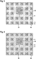
- FIG 2 shows a section through the transistor 1, in which the embedded shielding areas 7 are visible.
- a cellular structure is evident.
- a first cell 40 consists, for example, of the channel connection 5 of the second doping type and of the adjacent source connection 6. These first cells 40 are separated from one another by the shielding regions 7 of the electric field from the trench 8, which form a composite 30 of the shielding regions according to the invention, here a regular network by way of example, the invention not being restricted to a regular structural network.
- the first cells 40 are square, for example, but can also be rectangular, triangular, pentagonal, hexagonal, round, line-shaped, etc.
- the first cells 40 form a grid here, for example, between the composite 30 of the shielding regions. In this figure, this grid has a gap into which a second cell 50 is inserted.
- the second cell 50 consists of a common connection 23 both for the shielding regions 7 and for the diode connected in parallel. As in figure 1 these contacts can also be designed separately. This contact is correspondingly connected (not visible from this perspective) to the composite 30 of the shielding areas. According to the invention, the compound 30 of the shielding regions located below the trenches 8 is brought to the surface for contacting only at the second cells 50 . This saves a corresponding amount of area, since the lateral space requirement is reduced, and the current-carrying capacity per area is increased.
- figure 3 shows a section through the transistor 1, albeit in the preparation step with trenches 8 that have not yet been filled figure 2 .
- the invention also includes the case in which the trenches 8 are not connected and thus themselves form the first cells 40 of the cell array.
- figure 4 shows as well as figure 2 and 3 the cell array, with the gate electrodes 9 being introduced, which is located above the composite 30 of the shielding regions.
- the second cells 50 have, for example, a common connection 23 both for the shielding regions 7 and for the diode connected in parallel.
- figure 5 shows a cell field in which a third insulating layer 21 is applied above the gate electrode 9, which isolates the gate electrode 9 from the environment. Also integrated in the second cell 50 is a connection 19 for shielding regions, here embodied on the edge of the second cell 50 by way of example, and the diode connection 17, here embodied in the interior of the second cell 50 by way of example.
- figure 6 12 shows a cell array of a transistor 1 with a plurality of second cells 50. All of the first cells 40 form a grid which has gaps into which the second cells 50 are inserted.
- the second cells 50 themselves form a lattice, a superlattice 60. These have, for example, a common connection 23 both for the shielding regions 7 and for the diode.
- the invention is not limited to a superlattice 60.
- the second cells 50 can also be randomly distributed in the cell field of the first cells 40, or only a single second cell 50 is responsible as a contact for the integrated diode connected in parallel or as a connection 19 for the shielding regions 7. In this case, the cells are designed as squares, for example.
- the invention is not limited to this type of cells; triangles, rectangles, pentagons, hexagons, etc. can also be used.
- the arrangement of the second cells 50 and/or first cells 40 can also have a different structure than the square lattice structure implemented in this case, i.e., for example, rectangular, triangular, pentagonal, hexagonal, etc.
- first cells 40 and second cells 50 do not have to be the same.
- the square structure selected in the exemplary embodiment has the advantage that it enables a particularly simple and quick manufacturing process.
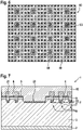
- figure 7 1 shows a side view of a transistor 1 similar to FIG figure 1 , but without a diode connected in parallel. Unlike in figure 1 the diode connection 17 shown there is combined with the connection 19 for the shielding regions to form a common connection 23 and is lowered together. The depth of these connections corresponds here, for example, to the depth of the shielding areas 7.
- the invention has the advantage that an increased current-carrying capacity is ensured with the same area, as a result of which a reduction in the connections for the shielding areas 19 is achieved.
- the core of the invention is the composite 30 of the shielding regions below the trenches, as a result of which a contact point no longer has to be routed to the surface at each trench.
- regular cell structures with both a lattice of first cells 40 and a superimposed lattice of second cells 50 are proposed, which have the advantage of simple manufacture as well as stable operation.
Landscapes
- Engineering & Computer Science (AREA)
- Microelectronics & Electronic Packaging (AREA)
- Power Engineering (AREA)
- Physics & Mathematics (AREA)
- Condensed Matter Physics & Semiconductors (AREA)
- General Physics & Mathematics (AREA)
- Computer Hardware Design (AREA)
- Ceramic Engineering (AREA)
- Manufacturing & Machinery (AREA)
- Electrodes Of Semiconductors (AREA)
- Metal-Oxide And Bipolar Metal-Oxide Semiconductor Integrated Circuits (AREA)
Applications Claiming Priority (2)
| Application Number | Priority Date | Filing Date | Title |
|---|---|---|---|
| DE102015224965.4A DE102015224965A1 (de) | 2015-12-11 | 2015-12-11 | Flächenoptimierter Transistor mit Superlattice-Strukturen |
| PCT/EP2016/075034 WO2017097482A1 (de) | 2015-12-11 | 2016-10-19 | Halbleitertransistor mit superlattice-strukturen |
Publications (2)
| Publication Number | Publication Date |
|---|---|
| EP3387677A1 EP3387677A1 (de) | 2018-10-17 |
| EP3387677B1 true EP3387677B1 (de) | 2022-12-07 |
Family
ID=57153474
Family Applications (1)
| Application Number | Title | Priority Date | Filing Date |
|---|---|---|---|
| EP16784179.0A Active EP3387677B1 (de) | 2015-12-11 | 2016-10-19 | Halbleitertransistor mit superlattice-strukturen |
Country Status (7)
| Country | Link |
|---|---|
| US (1) | US10460931B2 (ja) |
| EP (1) | EP3387677B1 (ja) |
| JP (1) | JP2019504485A (ja) |
| CN (1) | CN108770377A (ja) |
| DE (1) | DE102015224965A1 (ja) |
| TW (1) | TWI714683B (ja) |
| WO (1) | WO2017097482A1 (ja) |
Family Cites Families (14)
| Publication number | Priority date | Publication date | Assignee | Title |
|---|---|---|---|---|
| US6049108A (en) | 1995-06-02 | 2000-04-11 | Siliconix Incorporated | Trench-gated MOSFET with bidirectional voltage clamping |
| WO2005065385A2 (en) * | 2003-12-30 | 2005-07-21 | Fairchild Semiconductor Corporation | Power semiconductor devices and methods of manufacture |
| US7405452B2 (en) * | 2004-02-02 | 2008-07-29 | Hamza Yilmaz | Semiconductor device containing dielectrically isolated PN junction for enhanced breakdown characteristics |
| US7875951B2 (en) | 2007-12-12 | 2011-01-25 | Infineon Technologies Austria Ag | Semiconductor with active component and method for manufacture |
| EP2091083A3 (en) | 2008-02-13 | 2009-10-14 | Denso Corporation | Silicon carbide semiconductor device including a deep layer |
| JP2011044513A (ja) | 2009-08-20 | 2011-03-03 | National Institute Of Advanced Industrial Science & Technology | 炭化珪素半導体装置 |
| DE112011104322T5 (de) * | 2010-12-10 | 2013-10-02 | Mitsubishi Electric Corporation | Halbleitervorrichtung und Verfahren zur Herstellung einer Halbleitervorrichtung |
| JP5858933B2 (ja) * | 2011-02-02 | 2016-02-10 | ローム株式会社 | 半導体装置 |
| JP2013219293A (ja) * | 2012-04-12 | 2013-10-24 | Sumitomo Electric Ind Ltd | 炭化珪素半導体装置 |
| US8680614B2 (en) * | 2012-06-12 | 2014-03-25 | Monolithic Power Systems, Inc. | Split trench-gate MOSFET with integrated Schottky diode |
| JP5751213B2 (ja) * | 2012-06-14 | 2015-07-22 | 株式会社デンソー | 炭化珪素半導体装置およびその製造方法 |
| TW201423993A (zh) * | 2012-12-07 | 2014-06-16 | Ind Tech Res Inst | 具有分段式電場屏蔽區之碳化矽溝槽式閘極電晶體及其製造方法 |
| US8963240B2 (en) * | 2013-04-26 | 2015-02-24 | Alpha And Omega Semiconductor Incorporated | Shielded gate trench (SGT) mosfet devices and manufacturing processes |
| JP6135364B2 (ja) * | 2013-07-26 | 2017-05-31 | 住友電気工業株式会社 | 炭化珪素半導体装置およびその製造方法 |
-
2015
- 2015-12-11 DE DE102015224965.4A patent/DE102015224965A1/de not_active Withdrawn
-
2016
- 2016-10-19 US US16/060,612 patent/US10460931B2/en active Active
- 2016-10-19 JP JP2018529980A patent/JP2019504485A/ja active Pending
- 2016-10-19 EP EP16784179.0A patent/EP3387677B1/de active Active
- 2016-10-19 WO PCT/EP2016/075034 patent/WO2017097482A1/de active Application Filing
- 2016-10-19 CN CN201680072531.9A patent/CN108770377A/zh active Pending
- 2016-12-09 TW TW105140833A patent/TWI714683B/zh active
Also Published As
| Publication number | Publication date |
|---|---|
| EP3387677A1 (de) | 2018-10-17 |
| TW201724503A (zh) | 2017-07-01 |
| CN108770377A (zh) | 2018-11-06 |
| WO2017097482A1 (de) | 2017-06-15 |
| US10460931B2 (en) | 2019-10-29 |
| JP2019504485A (ja) | 2019-02-14 |
| DE102015224965A1 (de) | 2017-06-14 |
| TWI714683B (zh) | 2021-01-01 |
| US20180374698A1 (en) | 2018-12-27 |
Similar Documents
| Publication | Publication Date | Title |
|---|---|---|
| DE112014000679B4 (de) | Isolierschichtsiliciumcarbidhalbleiterbauteil und Verfahren zu dessen Herstellung | |
| DE102005052734B4 (de) | Halbleiterstruktur, Verfahren zum Betreiben einer Halbleiterstruktur und Verfahren zum Herstellen einer Halbleiterstruktur | |
| DE112012002823B4 (de) | Bipolartransistor mit isoliertem Gate und Verfahren zur Herstellung eines solchen Bipolartransistors | |
| DE19701189B4 (de) | Halbleiterbauteil | |
| DE102013204252B4 (de) | Halbleiterbauelement | |
| DE102014110366B4 (de) | Mos-leistungstransistor mit integriertem gatewiderstand | |
| DE102014117767B4 (de) | Halbleitervorrichtung mit rekombinationsbereich | |
| DE102004022455B4 (de) | Bipolartransistor mit isolierter Steuerelektrode | |
| DE112011104322T5 (de) | Halbleitervorrichtung und Verfahren zur Herstellung einer Halbleitervorrichtung | |
| AT505176A2 (de) | Grabenfeldplattenabschluss für leistungsvorrichtungen | |
| DE19811297A1 (de) | MOS-Halbleitervorrichtung mit hoher Durchbruchspannung | |
| DE102015121497B4 (de) | Halbleitervorrichtung mit einem ersten gategraben und einem zweiten gategraben | |
| DE10322594A1 (de) | MIS-Halbleiterbauteil und Verfahren zu seiner Herstellung | |
| DE112009004595T5 (de) | Halbleitervorrichtung | |
| DE112013006905B4 (de) | IGBT mit Verwendung einer Grabengateelektrode | |
| DE112007000803T5 (de) | Ladungsgleichgewichtstechniken für Leistungsvorrichtungen | |
| DE102008032547A1 (de) | Grabenisoliertes Gate-MOS-Halbleiterbauelement | |
| DE102008055819A1 (de) | Halbleiterbauelement mit Gates eines vertikalen und eines horizontalen Typs und Verfahren zu seiner Herstellung | |
| DE102020116653B4 (de) | Siliziumcarbid-halbleiterbauelement | |
| DE112014001296T5 (de) | Leistungshalbleitervorrichtung und entsprechendes Modul | |
| DE112012000954T5 (de) | Leistungshalbleiterbauelement und Verfahren zum Herstellen eines derartigen Leistungshalbleiterbauelements | |
| DE69930715T2 (de) | Elektronische Halbleiterleistung mit integrierter Diode | |
| DE102018126026A1 (de) | Akkumulationsverstärkter bipolartransistor mit isolierter gate-elektrode (accumulation enhanced insulated gate bipolar transistor, aegt) und verfahren zu dessen verwendung | |
| DE102005048447B4 (de) | Halbleiterleistungsbauelement mit Ladungskompensationsstruktur und Verfahren zur Herstellung desselben | |
| DE102004047772B4 (de) | Lateraler Halbleitertransistor |
Legal Events
| Date | Code | Title | Description |
|---|---|---|---|
| STAA | Information on the status of an ep patent application or granted ep patent |
Free format text: STATUS: UNKNOWN |
|
| STAA | Information on the status of an ep patent application or granted ep patent |
Free format text: STATUS: THE INTERNATIONAL PUBLICATION HAS BEEN MADE |
|
| PUAI | Public reference made under article 153(3) epc to a published international application that has entered the european phase |
Free format text: ORIGINAL CODE: 0009012 |
|
| STAA | Information on the status of an ep patent application or granted ep patent |
Free format text: STATUS: REQUEST FOR EXAMINATION WAS MADE |
|
| 17P | Request for examination filed |
Effective date: 20180711 |
|
| AK | Designated contracting states |
Kind code of ref document: A1 Designated state(s): AL AT BE BG CH CY CZ DE DK EE ES FI FR GB GR HR HU IE IS IT LI LT LU LV MC MK MT NL NO PL PT RO RS SE SI SK SM TR |
|
| AX | Request for extension of the european patent |
Extension state: BA ME |
|
| DAV | Request for validation of the european patent (deleted) | ||
| DAX | Request for extension of the european patent (deleted) | ||
| RAP1 | Party data changed (applicant data changed or rights of an application transferred) |
Owner name: ROBERT BOSCH GMBH |
|
| STAA | Information on the status of an ep patent application or granted ep patent |
Free format text: STATUS: EXAMINATION IS IN PROGRESS |
|
| 17Q | First examination report despatched |
Effective date: 20210218 |
|
| STAA | Information on the status of an ep patent application or granted ep patent |
Free format text: STATUS: EXAMINATION IS IN PROGRESS |
|
| GRAP | Despatch of communication of intention to grant a patent |
Free format text: ORIGINAL CODE: EPIDOSNIGR1 |
|
| STAA | Information on the status of an ep patent application or granted ep patent |
Free format text: STATUS: GRANT OF PATENT IS INTENDED |
|
| INTG | Intention to grant announced |
Effective date: 20220825 |
|
| GRAS | Grant fee paid |
Free format text: ORIGINAL CODE: EPIDOSNIGR3 |
|
| GRAA | (expected) grant |
Free format text: ORIGINAL CODE: 0009210 |
|
| STAA | Information on the status of an ep patent application or granted ep patent |
Free format text: STATUS: THE PATENT HAS BEEN GRANTED |
|
| AK | Designated contracting states |
Kind code of ref document: B1 Designated state(s): AL AT BE BG CH CY CZ DE DK EE ES FI FR GB GR HR HU IE IS IT LI LT LU LV MC MK MT NL NO PL PT RO RS SE SI SK SM TR |
|
| REG | Reference to a national code |
Ref country code: GB Ref legal event code: FG4D Free format text: NOT ENGLISH |
|
| REG | Reference to a national code |
Ref country code: CH Ref legal event code: EP Ref country code: AT Ref legal event code: REF Ref document number: 1536820 Country of ref document: AT Kind code of ref document: T Effective date: 20221215 |
|
| REG | Reference to a national code |
Ref country code: DE Ref legal event code: R096 Ref document number: 502016015470 Country of ref document: DE |
|
| REG | Reference to a national code |
Ref country code: IE Ref legal event code: FG4D Free format text: LANGUAGE OF EP DOCUMENT: GERMAN |
|
| REG | Reference to a national code |
Ref country code: LT Ref legal event code: MG9D |
|
| REG | Reference to a national code |
Ref country code: NL Ref legal event code: MP Effective date: 20221207 |
|
| PG25 | Lapsed in a contracting state [announced via postgrant information from national office to epo] |
Ref country code: SE Free format text: LAPSE BECAUSE OF FAILURE TO SUBMIT A TRANSLATION OF THE DESCRIPTION OR TO PAY THE FEE WITHIN THE PRESCRIBED TIME-LIMIT Effective date: 20221207 Ref country code: NO Free format text: LAPSE BECAUSE OF FAILURE TO SUBMIT A TRANSLATION OF THE DESCRIPTION OR TO PAY THE FEE WITHIN THE PRESCRIBED TIME-LIMIT Effective date: 20230307 Ref country code: LT Free format text: LAPSE BECAUSE OF FAILURE TO SUBMIT A TRANSLATION OF THE DESCRIPTION OR TO PAY THE FEE WITHIN THE PRESCRIBED TIME-LIMIT Effective date: 20221207 Ref country code: FI Free format text: LAPSE BECAUSE OF FAILURE TO SUBMIT A TRANSLATION OF THE DESCRIPTION OR TO PAY THE FEE WITHIN THE PRESCRIBED TIME-LIMIT Effective date: 20221207 Ref country code: ES Free format text: LAPSE BECAUSE OF FAILURE TO SUBMIT A TRANSLATION OF THE DESCRIPTION OR TO PAY THE FEE WITHIN THE PRESCRIBED TIME-LIMIT Effective date: 20221207 |
|
| PG25 | Lapsed in a contracting state [announced via postgrant information from national office to epo] |
Ref country code: RS Free format text: LAPSE BECAUSE OF FAILURE TO SUBMIT A TRANSLATION OF THE DESCRIPTION OR TO PAY THE FEE WITHIN THE PRESCRIBED TIME-LIMIT Effective date: 20221207 Ref country code: PL Free format text: LAPSE BECAUSE OF FAILURE TO SUBMIT A TRANSLATION OF THE DESCRIPTION OR TO PAY THE FEE WITHIN THE PRESCRIBED TIME-LIMIT Effective date: 20221207 Ref country code: LV Free format text: LAPSE BECAUSE OF FAILURE TO SUBMIT A TRANSLATION OF THE DESCRIPTION OR TO PAY THE FEE WITHIN THE PRESCRIBED TIME-LIMIT Effective date: 20221207 Ref country code: HR Free format text: LAPSE BECAUSE OF FAILURE TO SUBMIT A TRANSLATION OF THE DESCRIPTION OR TO PAY THE FEE WITHIN THE PRESCRIBED TIME-LIMIT Effective date: 20221207 Ref country code: GR Free format text: LAPSE BECAUSE OF FAILURE TO SUBMIT A TRANSLATION OF THE DESCRIPTION OR TO PAY THE FEE WITHIN THE PRESCRIBED TIME-LIMIT Effective date: 20230308 |
|
| PG25 | Lapsed in a contracting state [announced via postgrant information from national office to epo] |
Ref country code: NL Free format text: LAPSE BECAUSE OF FAILURE TO SUBMIT A TRANSLATION OF THE DESCRIPTION OR TO PAY THE FEE WITHIN THE PRESCRIBED TIME-LIMIT Effective date: 20221207 |
|
| PG25 | Lapsed in a contracting state [announced via postgrant information from national office to epo] |
Ref country code: SM Free format text: LAPSE BECAUSE OF FAILURE TO SUBMIT A TRANSLATION OF THE DESCRIPTION OR TO PAY THE FEE WITHIN THE PRESCRIBED TIME-LIMIT Effective date: 20221207 Ref country code: RO Free format text: LAPSE BECAUSE OF FAILURE TO SUBMIT A TRANSLATION OF THE DESCRIPTION OR TO PAY THE FEE WITHIN THE PRESCRIBED TIME-LIMIT Effective date: 20221207 Ref country code: PT Free format text: LAPSE BECAUSE OF FAILURE TO SUBMIT A TRANSLATION OF THE DESCRIPTION OR TO PAY THE FEE WITHIN THE PRESCRIBED TIME-LIMIT Effective date: 20230410 Ref country code: EE Free format text: LAPSE BECAUSE OF FAILURE TO SUBMIT A TRANSLATION OF THE DESCRIPTION OR TO PAY THE FEE WITHIN THE PRESCRIBED TIME-LIMIT Effective date: 20221207 Ref country code: CZ Free format text: LAPSE BECAUSE OF FAILURE TO SUBMIT A TRANSLATION OF THE DESCRIPTION OR TO PAY THE FEE WITHIN THE PRESCRIBED TIME-LIMIT Effective date: 20221207 |
|
| PG25 | Lapsed in a contracting state [announced via postgrant information from national office to epo] |
Ref country code: SK Free format text: LAPSE BECAUSE OF FAILURE TO SUBMIT A TRANSLATION OF THE DESCRIPTION OR TO PAY THE FEE WITHIN THE PRESCRIBED TIME-LIMIT Effective date: 20221207 Ref country code: IS Free format text: LAPSE BECAUSE OF FAILURE TO SUBMIT A TRANSLATION OF THE DESCRIPTION OR TO PAY THE FEE WITHIN THE PRESCRIBED TIME-LIMIT Effective date: 20230407 Ref country code: AL Free format text: LAPSE BECAUSE OF FAILURE TO SUBMIT A TRANSLATION OF THE DESCRIPTION OR TO PAY THE FEE WITHIN THE PRESCRIBED TIME-LIMIT Effective date: 20221207 |
|
| REG | Reference to a national code |
Ref country code: DE Ref legal event code: R097 Ref document number: 502016015470 Country of ref document: DE |
|
| PLBE | No opposition filed within time limit |
Free format text: ORIGINAL CODE: 0009261 |
|
| STAA | Information on the status of an ep patent application or granted ep patent |
Free format text: STATUS: NO OPPOSITION FILED WITHIN TIME LIMIT |
|
| PG25 | Lapsed in a contracting state [announced via postgrant information from national office to epo] |
Ref country code: DK Free format text: LAPSE BECAUSE OF FAILURE TO SUBMIT A TRANSLATION OF THE DESCRIPTION OR TO PAY THE FEE WITHIN THE PRESCRIBED TIME-LIMIT Effective date: 20221207 |
|
| 26N | No opposition filed |
Effective date: 20230908 |
|
| PG25 | Lapsed in a contracting state [announced via postgrant information from national office to epo] |
Ref country code: SI Free format text: LAPSE BECAUSE OF FAILURE TO SUBMIT A TRANSLATION OF THE DESCRIPTION OR TO PAY THE FEE WITHIN THE PRESCRIBED TIME-LIMIT Effective date: 20221207 |
|
| PGFP | Annual fee paid to national office [announced via postgrant information from national office to epo] |
Ref country code: IT Payment date: 20231031 Year of fee payment: 8 Ref country code: FR Payment date: 20231023 Year of fee payment: 8 |
|
| PGFP | Annual fee paid to national office [announced via postgrant information from national office to epo] |
Ref country code: DE Payment date: 20231218 Year of fee payment: 8 |