EP3386089A1 - Leistungsmodul - Google Patents
Leistungsmodul Download PDFInfo
- Publication number
- EP3386089A1 EP3386089A1 EP17827253.0A EP17827253A EP3386089A1 EP 3386089 A1 EP3386089 A1 EP 3386089A1 EP 17827253 A EP17827253 A EP 17827253A EP 3386089 A1 EP3386089 A1 EP 3386089A1
- Authority
- EP
- European Patent Office
- Prior art keywords
- circuit
- low
- programmable circuit
- signal
- terminal
- Prior art date
- Legal status (The legal status is an assumption and is not a legal conclusion. Google has not performed a legal analysis and makes no representation as to the accuracy of the status listed.)
- Granted
Links
Images




Classifications
-
- H—ELECTRICITY
- H02—GENERATION; CONVERSION OR DISTRIBUTION OF ELECTRIC POWER
- H02M—APPARATUS FOR CONVERSION BETWEEN AC AND AC, BETWEEN AC AND DC, OR BETWEEN DC AND DC, AND FOR USE WITH MAINS OR SIMILAR POWER SUPPLY SYSTEMS; CONVERSION OF DC OR AC INPUT POWER INTO SURGE OUTPUT POWER; CONTROL OR REGULATION THEREOF
- H02M1/00—Details of apparatus for conversion
- H02M1/08—Circuits specially adapted for the generation of control voltages for semiconductor devices incorporated in static converters
-
- H—ELECTRICITY
- H02—GENERATION; CONVERSION OR DISTRIBUTION OF ELECTRIC POWER
- H02M—APPARATUS FOR CONVERSION BETWEEN AC AND AC, BETWEEN AC AND DC, OR BETWEEN DC AND DC, AND FOR USE WITH MAINS OR SIMILAR POWER SUPPLY SYSTEMS; CONVERSION OF DC OR AC INPUT POWER INTO SURGE OUTPUT POWER; CONTROL OR REGULATION THEREOF
- H02M1/00—Details of apparatus for conversion
- H02M1/08—Circuits specially adapted for the generation of control voltages for semiconductor devices incorporated in static converters
- H02M1/088—Circuits specially adapted for the generation of control voltages for semiconductor devices incorporated in static converters for the simultaneous control of series or parallel connected semiconductor devices
-
- H—ELECTRICITY
- H02—GENERATION; CONVERSION OR DISTRIBUTION OF ELECTRIC POWER
- H02M—APPARATUS FOR CONVERSION BETWEEN AC AND AC, BETWEEN AC AND DC, OR BETWEEN DC AND DC, AND FOR USE WITH MAINS OR SIMILAR POWER SUPPLY SYSTEMS; CONVERSION OF DC OR AC INPUT POWER INTO SURGE OUTPUT POWER; CONTROL OR REGULATION THEREOF
- H02M1/00—Details of apparatus for conversion
- H02M1/32—Means for protecting converters other than automatic disconnection
-
- H—ELECTRICITY
- H02—GENERATION; CONVERSION OR DISTRIBUTION OF ELECTRIC POWER
- H02M—APPARATUS FOR CONVERSION BETWEEN AC AND AC, BETWEEN AC AND DC, OR BETWEEN DC AND DC, AND FOR USE WITH MAINS OR SIMILAR POWER SUPPLY SYSTEMS; CONVERSION OF DC OR AC INPUT POWER INTO SURGE OUTPUT POWER; CONTROL OR REGULATION THEREOF
- H02M7/00—Conversion of AC power input into DC power output; Conversion of DC power input into AC power output
- H02M7/42—Conversion of DC power input into AC power output without possibility of reversal
- H02M7/44—Conversion of DC power input into AC power output without possibility of reversal by static converters
- H02M7/48—Conversion of DC power input into AC power output without possibility of reversal by static converters using discharge tubes with control electrode or semiconductor devices with control electrode
- H02M7/53—Conversion of DC power input into AC power output without possibility of reversal by static converters using discharge tubes with control electrode or semiconductor devices with control electrode using devices of a triode or transistor type requiring continuous application of a control signal
- H02M7/537—Conversion of DC power input into AC power output without possibility of reversal by static converters using discharge tubes with control electrode or semiconductor devices with control electrode using devices of a triode or transistor type requiring continuous application of a control signal using semiconductor devices only, e.g. single switched pulse inverters
- H02M7/538—Conversion of DC power input into AC power output without possibility of reversal by static converters using discharge tubes with control electrode or semiconductor devices with control electrode using devices of a triode or transistor type requiring continuous application of a control signal using semiconductor devices only, e.g. single switched pulse inverters in a push-pull configuration
-
- H—ELECTRICITY
- H02—GENERATION; CONVERSION OR DISTRIBUTION OF ELECTRIC POWER
- H02M—APPARATUS FOR CONVERSION BETWEEN AC AND AC, BETWEEN AC AND DC, OR BETWEEN DC AND DC, AND FOR USE WITH MAINS OR SIMILAR POWER SUPPLY SYSTEMS; CONVERSION OF DC OR AC INPUT POWER INTO SURGE OUTPUT POWER; CONTROL OR REGULATION THEREOF
- H02M7/00—Conversion of AC power input into DC power output; Conversion of DC power input into AC power output
- H02M7/42—Conversion of DC power input into AC power output without possibility of reversal
- H02M7/44—Conversion of DC power input into AC power output without possibility of reversal by static converters
- H02M7/48—Conversion of DC power input into AC power output without possibility of reversal by static converters using discharge tubes with control electrode or semiconductor devices with control electrode
- H02M7/53—Conversion of DC power input into AC power output without possibility of reversal by static converters using discharge tubes with control electrode or semiconductor devices with control electrode using devices of a triode or transistor type requiring continuous application of a control signal
- H02M7/537—Conversion of DC power input into AC power output without possibility of reversal by static converters using discharge tubes with control electrode or semiconductor devices with control electrode using devices of a triode or transistor type requiring continuous application of a control signal using semiconductor devices only, e.g. single switched pulse inverters
- H02M7/5387—Conversion of DC power input into AC power output without possibility of reversal by static converters using discharge tubes with control electrode or semiconductor devices with control electrode using devices of a triode or transistor type requiring continuous application of a control signal using semiconductor devices only, e.g. single switched pulse inverters in a bridge configuration
-
- H—ELECTRICITY
- H02—GENERATION; CONVERSION OR DISTRIBUTION OF ELECTRIC POWER
- H02M—APPARATUS FOR CONVERSION BETWEEN AC AND AC, BETWEEN AC AND DC, OR BETWEEN DC AND DC, AND FOR USE WITH MAINS OR SIMILAR POWER SUPPLY SYSTEMS; CONVERSION OF DC OR AC INPUT POWER INTO SURGE OUTPUT POWER; CONTROL OR REGULATION THEREOF
- H02M1/00—Details of apparatus for conversion
- H02M1/0003—Details of control, feedback or regulation circuits
- H02M1/0009—Devices or circuits for detecting current in a converter
Definitions
- the embodiments discussed herein relate to a power module that includes switching elements connected in a half-bridge configuration and a drive circuit for driving these switching elements and that is able to implement a desired logic function or parameter in the drive circuit.
- HVIC high voltage integrated circuit
- the HVIC includes a high-side circuit for controlling the high-side switching element of the half-bridge circuit and a low-side circuit for controlling the low-side switching element of the half-bridge circuit.
- a power module has a function of protecting it from a drop in power supply voltage, overcurrent, and overheat.
- a priority order of alarming that is made when a voltage drop, overcurrent, or overheat is detected.
- a threshold to be used for detecting the voltage drop, overcurrent, or overheat.
- a high-side programmable circuit connected to a high-side circuit is referenced to a midpoint potential of a half-bridge, and a low-side programmable circuit connected to a low-side circuit is referenced to ground.
- the reference potential for the high-side circuit and the high-side programmable circuit varies between zero volt (V) and the power supply voltage (for example, several hundred volts) by two switching elements complementarily being switched on and off.
- the device taught in Patent Literature 1 has one system although a power system for a write circuit is independent of a power system for a programmable circuit that communicates with the write circuit, and has a reference potential that does not vary every moment, unlike the reference potential for the high-side circuit of the power module. Therefore, it is not possible to use the write circuit configured as taught in Patent Literature 1, for the high-side programmable circuit and the low-side programmable circuit. That is to say, the power module needs a write circuit for the high-side programmable circuit and a write circuit for the low-side programmable circuit separately. In addition, since the high-side reference potential may rise to a very high voltage level, the high-side write circuit and the low-side write circuit need to be provided physically separated from each other.
- Patent Literature 1 Japanese National Publication of International Patent Application No. 2014-515843 (Paragraphs [0078] and [0087], and FIG. 2 )
- the present invention has been made in view of these circumstances, and an object thereof is to provide a small-size power module that has one system for a program control signal to be input to programmable circuits.
- a power module including: a first high-side switching element and a second low-side switching element that are connected in a half-bridge configuration; an integrated circuit including a high-side circuit that drives the first switching element and a low-side circuit that drives the second switching element; a high-side programmable circuit that is able to implement a desired first logic function or parameter to be used by the high-side circuit; and a low-side programmable circuit that is able to implement a desired second logic function or parameter to be used by the low-side circuit.
- the integrated circuit of this power module includes a write port that receives data of one system for a program control signal to be written to the high-side programmable circuit and the low-side programmable circuit, internal wiring that connects the high-side programmable circuit and the low-side programmable circuit in a daisy chain configuration, and a level shifter that is provided on the internal wiring connected to the high-side programmable circuit and that connects a low-side signal system and a high-side signal system.
- the power module configured as above is small in size because it has one system for a signal to be input to programmable circuits and uses a level shifter to form a daisy chain.
- FIG. 1 is a circuit diagram illustrating a configuration of a power module according to one embodiment.
- the power module 10 of the embodiment includes switching elements XMH and XML connected in a half-bridge configuration, an HVIC 11, a high-side programmable circuit 12, a low-side programmable circuit 13, and power supplies VCCH and VCCL.
- MOSFETs Metal-Oxide-Semiconductor Field Effect Transistor
- the drain terminal of the switching element XMH is connected to the anode terminal of a high-voltage power supply HV
- the source terminal of the switching element XML is connected to the cathode terminal of the high-voltage power supply HV and a ground terminal GND of the HVIC 11.
- the HVIC 11 includes a high-side circuit HS and a low-side circuit LS.
- the high-side circuit HS drives the high-side switching element XMH, and has an output terminal HO connected to the gate terminal of the switching element XMH.
- the high-side circuit HS also has a power supply terminal VB connected to the anode terminal of the power supply VCCH and a reference potential terminal VS connected to the cathode terminal of the power supply VCCH.
- the reference potential terminal VS is also connected to a connecting point between the switching elements XMH and XML.
- the low-side circuit LS drives the lower-side switching element XML, and has an output terminal LO connected to the gate terminal of the switching element XML.
- the low-side circuit LS also has a power supply terminal VCC connected to the anode terminal of the power supply VCCL and the ground terminal GND connected to the cathode terminal of the power supply VCCL.
- the high-side programmable circuit 12 is connected to the high-side circuit HS with an input/output bus IOH.
- a power supply feeding terminal V5H and the reference potential terminal VS of the high-side circuit HS are connected to both power feeding terminals of the high-side programmable circuit 12 and both terminals of a capacitor C1H.
- the low-side programmable circuit 13 is connected to the low-side circuit LS with an input/output bus IOL.
- a power supply feeding terminal V5L and the ground terminal GND of the low-side circuit LS are connected to both power feeding terminals of the low-side programmable circuit 13 and both terminals of a capacitor C1L.
- the power module 10 is connected to signal lines through which the low-side circuit LS of the HVIC 11 receives a high-side control signal HIN and a low-side control signal LIN from a control circuit 20.
- the power module 10 has a write port for receiving data for a program control signal to be written to the high-side programmable circuit 12 and low-side programmable circuit 13, and the low-side circuit LS and the control circuit 20 are connected via this write port.
- the program control signal is a JTAG control signal, for example, and the low-side circuit LS and the control circuit 20 are connected with four signal lines for sending and receiving signals TMS (Test Mode Select), TCK (Test Clock), TDI (Test Data In), and TDO (Test Data Out).
- terminals to which these four signal lines are connected function as the write port for one system.
- the high-side circuit HS and low-side circuit LS of the HVIC 11 are connected with signal lines for transferring signals SET and RESET, which correspond to the high-side control signal HIN.
- the high-side circuit HS and low-side circuit LS are connected with signal lines for transferring signals HTMS, HTCK, HTDI, and HTDO, which correspond to the signals TMS, TCK, TDI, and TDO, respectively.
- the low-side circuit LS is provided with a level shifter that raises the levels of the signals TMS, TCK, TDI, and TDO to generate the signals HTMS, HTCK, HTDI, and HTDO and that drops the level of the signal HTDO output from the high-side circuit HS.
- the control circuit 20 writes and rewrites data to the high-side programmable circuit 12 and the low-side programmable circuit 13. More specifically, the signals TMS and TCK input from the control circuit 20 to the power module 10 are supplied to the low-side programmable circuit 13 as they are, and the signals TMS and TCK are level-shifted to the signals HTMS and HTCK, which are then supplied to the high-side programmable circuit 12.
- the signal TDI is supplied to the low-side programmable circuit 13 as it is, and the signal TDI is level-shifted to the signal HTDI, which is then supplied to the high-side programmable circuit 12.
- the signal TDO is output from the low-side programmable circuit 13 as it is, and the signal HTDO is output from the high-side programmable circuit 12.
- a program control signal for the high-side programmable circuit 12 and the low-side programmable circuit 13 is transferred in a daisy chain fashion. More specifically, the signal TDI input from the control circuit 20 is level-shifted to the signal HTDI, which is then supplied to the high-side programmable circuit 12. The signal HTDO output from the high-side programmable circuit 12 is level-shifted by the level shifter and is then supplied to the low-side programmable circuit 13, and the low-side programmable circuit 13 outputs the signal TDO.
- the signal TDI input from the control circuit 20 is supplied to the low-side programmable circuit 13, and the signal TDO output from the low-side programmable circuit 13 is level-shifted to the signal HTDI, which is then supplied to the high-side programmable circuit 12.
- the signal HTDO output from the high-side programmable circuit 12 is level-shifted to the signal TDO.
- the power module 10 When the power module 10 receives the signal HIN from the control circuit 20, it converts the signal HIN to a signal SET, RESET, which is then supplied to the high-side circuit HS.
- the high-side circuit HS generates a gate drive signal on the basis of the signal SET, RESET. This gate drive signal is output from the output terminal HO, and is supplied to the gate terminal of the switching element XMH to perform on-off control of the switching element XMH.
- the power module 10 receives the signal LIN from the control circuit 20, on the other hand, the signal LIN is input to the low-side circuit LS.
- the low-side circuit LS generates a gate drive signal on the basis of the signal LIN. This gate drive signal is output from the output terminal LO and is supplied to the gate terminal of the switching element XML to perform on-off control of the switching element XML.
- FIG. 2 is a circuit diagram illustrating an example of a configuration of a power module according to a first embodiment.
- FIG. 3 illustrates a connection relationship between signal lines to be used for a JTAG control signal.
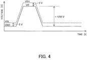
- FIG. 4 is a waveform diagram illustrating a relationship in reference potential between a high-side circuit and a low-side circuit.
- the same reference numerals as in FIG. 1 denote the same or equivalent structural elements in FIGS. 2 and 3 , and the detailed description about these structural elements will not be repeated.
- an HVIC 11 includes a high-side circuit HS and a low-side circuit LS as illustrated in FIG. 2 .
- a level shifter 14 for connecting the high-side signal system and the low-side signal system is provided at a connecting point between the high-side circuit HS and the low-side circuit LS.
- the high-side circuit HS includes a 5V regulator 15 that is connected to a power supply terminal VB and generates a 5V voltage from the voltage of a power supply VCCH, a high-side drive circuit 16 that outputs a gate drive signal for controlling a switching element XMH to an output terminal HO, and inverters INV1 to INV4.
- the high-side drive circuit 16 is connected to a high-side programmable circuit 12 with an input/output bus IOH.
- this high-side programmable circuit 12 is made up of an FPGA (Field Programmable Gate Array), which is able to implement a desired logic function or parameter.
- the high-side programmable circuit 12 has terminals tms, tck, and tdi connected to the output terminals of the inverters INV1, INV2, and INV3 of the high-side circuit HS, respectively.
- the high-side programmable circuit 12 also has a terminal tdo connected to the input terminal of the inverter INV4 of the high-side circuit HS.
- the high-side programmable circuit 12 has a logic cell 12a that is connected to the terminals tdi and tdo and that forms a desired logic function or the like. For example, a detection threshold (parameter) for a protection circuit built in the high-side drive circuit 16 is written to this logic cell 12a by using data that is input via the terminal tdi, and the written parameter is transferred to the high-side drive circuit 16 through the input/output bus IOH at the normal operation.
- the high-side programmable circuit 12 is connected to a power supply feeding terminal V5H and a high-side reference potential terminal VS and is supplied with power from the 5V regulator 15.
- the low-side circuit LS includes a 5V regulator 17 that is connected to a power supply terminal VCC and generates a 5V voltage from the voltage of a power supply VCCL, a low-side control circuit 18, and a differential pulse generator 19.
- the low-side control circuit 18 is connected to a low-side programmable circuit 13 with an input/output bus IOL.
- This low-side programmable circuit 13 is made up of an FPGA, for example.
- the low-side programmable circuit 13 has terminals tms, tck, tdi, and tdo connected to signal lines corresponding to a write port that is provided for JTAG control signals in the low-side circuit LS.
- the low-side programmable circuit 13 includes a logic cell 13a that is connected to the terminals tdi and tdo and that forms a desired logic function or the like.
- a detection threshold (parameter) for a protection circuit built in the low-side control circuit 18 is written to this logic cell 13a by using data that is input via the terminal tdi, for example, and the written parameter is transferred to the low-side control circuit 18 through the input/output bus IOL at the normal operation.
- the low-side programmable circuit 13 is connected to a power supply feeding terminal V5L and a ground terminal GND that has a low-side reference potential, and is supplied with power from the 5V regulator 17.
- the low-side control circuit 18 receives signals HIN and LIN, outputs a gate drive signal for controlling a switching element XML to an output terminal LO on the basis of the signal LIN, and outputs the signal HIN to the differential pulse generator 19.
- the differential pulse generator 19 receives the signal HIN, outputs a signal SET at rising edge timing of the signal HIN, and outputs a signal RESET at falling edge timing of the signal HIN.
- the level shifter 14 includes high breakdown-voltage transistors MN1 to MN5 and MP1, resistors R1 to R6, and diodes D1 to D6.
- the gate terminals of the transistors MN1 and MN2 are connected to the output terminals of the differential pulse generator 19, the drain terminals thereof are connected to the high-side drive circuit 16, and the source terminals thereof are connected to the ground terminal GND.
- the drain terminal of the transistor MN1 is also connected to one end of the resistor R1 and the cathode terminal of the diode D1.
- the other end of the resistor R1 is connected to the power supply of the high-side circuit HS, and the anode terminal of the diode D1 is connected to the reference potential terminal VS of the high-side circuit HS.
- the drain terminal of the transistor MN2 is also connected to one end of the resistor R2 and the cathode terminal of the diode D2.
- the other end of the resistor R2 is connected to the power supply of the high-side circuit HS, and the anode terminal of the diode D2 is connected to the reference potential terminal VS of the high-side circuit HS.
- the gate terminal of the transistor MN3 is connected to a terminal of the low-side circuit LS that receives a signal TMS, the drain terminal thereof is connected to the input terminal of the inverter INV1 of the high-side circuit HS, and the source terminal thereof is connected to the ground terminal GND.
- the drain terminal of the transistor MN3 is also connected to one end of the resistor R3 and the cathode terminal of the diode D3.
- the other end of the resistor R3 is connected to the power supply of the high-side circuit HS, and the anode terminal of the diode D3 is connected to the reference potential terminal VS of the high-side circuit HS.
- the gate terminal of the transistor MN4 is connected to a terminal of the low-side circuit LS that receives a signal TCK, the drain terminal thereof is connected to the input terminal of the inverter INV2 of the high-side circuit HS, and the source terminal thereof is connected to the ground terminal GND.
- the drain terminal of the transistor MN4 is also connected to one end of the resistor R4 and the cathode terminal of the diode D4.
- the other end of the resistor R4 is connected to the power supply of the high-side circuit HS, and the anode terminal of the diode D4 is connected to the reference potential terminal VS of the high-side circuit HS.
- the gate terminal of the transistor MN5 is connected to a terminal of the low-side circuit LS that receives a signal TDI, the drain terminal thereof is connected to the input terminal of the inverter INV3 of the high-side circuit HS, and the source terminal thereof is connected to the ground terminal GND.
- the drain terminal of the transistor MN5 is also connected to one end of the resistor R5 and the cathode terminal of the diode D5.
- the other end of the resistor R5 is connected to the power supply of the high-side circuit HS, and the anode terminal of the diode D5 is connected to the reference potential terminal VS of the high-side circuit HS.
- the gate terminal of the transistor MP1 is connected to the output terminal of the inverter INV4 of the high-side circuit HS, the source terminal thereof is connected to the power supply of the high-side circuit HS, and the drain terminal thereof is connected to the terminal tdi of the low-side programmable circuit 13.
- the drain terminal of the transistor MP1 is also connected to one end of the resistor R6 and the cathode terminal of the diode D6. The other end of the resistor R6 and the anode terminal of the diode D6 are connected to the ground terminal GND of the low-side circuit LS.
- the signal TDI is transferred, in series, to the high-side programmable circuit 12 and the low-side programmable circuit 13 that are connected via internal wiring in a daisy chain configuration (at this time, basically, the logic cells 12a and 13a output received data as it is, at timing delayed by clocks needed for operation), and the signal TDO is output from the low-side programmable circuit 13.
- signals are input to and output from the high-side programmable circuit 12 via the level shifter 14.
- the signal HIN when a signal HIN is input to the low-side control circuit 18, the signal HIN is input to the differential pulse generator 19, and differential pulses are output at the rising edge timing and falling edge timing of the signal HIN.
- These differential pulses are input to the gate terminals of the transistors MN1 and MN2 and are output from the drain terminals thereof to the high-side drive circuit 16 as signals SET and RESET, respectively.
- the high-side drive circuit 16 restores a gate signal for controlling the switching element XMH from the signals SET and RESET, and outputs the gate signal from the output terminal HO.
- the signal LIN is output from the output terminal LO as a gate signal for controlling the switching element XML.
- the voltage at the reference potential terminal VS is approximately equal to the voltage of the high voltage power supply HV.
- the voltage of the high voltage power supply HV is lower than 1200 V in this embodiment, and for example, is assumed to be as low as 400 V. Therefore, the power supply voltage for the high-side programmable circuit 12, that is, the voltage at the power supply feeding terminal V5H is higher by 5 V than the voltage at the reference potential terminal VS on the ground basis. This is a reason why the level shifter 14 is needed for inputs and outputs of JTAG control signals, which are input on the ground basis, to and from the high-side programmable circuit 12.
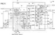
- FIG. 5 is a circuit diagram illustrating an example of a configuration of a power module according to a second embodiment.
- the same reference numerals as in FIG. 2 denote the same or equivalent structural elements in FIG. 5 , and the detailed description about these structural elements will not be repeated.
- the power module 10 of the first embodiment is modified so as to impose a restriction on timing for writing based on a JTAG control signal, thereby forming a power module 10a of the second embodiment. That is, the power module 10 of the first embodiment is able to execute writing and rewriting by using a JTAG control signal at any time.
- the power module 10a of the second embodiment is able to execute writing by using a JTAG control signal only when a high-side reference potential terminal VS is low. Therefore, a low-side circuit LS of an HVIC 11 has a JTAG signal control circuit 21 as a transfer timing control circuit for controlling timing of transferring a JTAG control signal.
- the JTAG signal control circuit 21 includes AND circuits AND1 to AND5.
- the negative logic input terminal of the AND circuit AND1 is configured to receive a signal HIN, and the positive logic input terminal thereof is configured to receive a signal LIN.
- the output terminal of the AND circuit AND1 is connected to one input terminal of each of the AND circuits AND2 to AND5.
- the other input terminal of the AND circuit AND2 is configured to receive a signal TMS, and the output terminal thereof is connected to the gate terminal of a transistor MN3.
- the other input terminal of the AND circuit AND3 is configured to receive a signal TCK, and the output terminal thereof is connected to the gate terminal of a transistor MN4.
- the other input terminal of the AND circuit AND4 is configured to receive a signal TDI, and the output terminal thereof is connected to the gate terminal of a transistor MN5.
- the other input terminal of the AND circuit AND5 is configured to receive a signal HTDO, and the output terminal thereof is connected to a terminal tdi of a low-side programmable circuit 13.
- the JTAG signal control circuit 21 when the signal HIN has a low (L) level and the signal LIN has a high (H) level, the output terminal of the AND circuit AND1 becomes an H level and an H level signal is input to the one input terminal of each of the AND circuits AND2 to AND5.
- the AND circuits AND2 to AND4 permit transfer of the signals TMS, TCK, and TDI, and the AND circuit AND5 permits transfer of the signal HTDO. That is to say, the JTAG signal control circuit 21 is able to execute data writing to the high-side programmable circuit 12 and low-side programmable circuit 13.
- the output terminal of the AND circuit AND1 has an L level under conditions other than those where the signal HIN has an L level and the signal LIN has an H level, and therefore the AND circuits AND2 to AND5 inhibit transfer of the signals. That is to say, the JTAG signal control circuit 21 inhibits data writing to the high-side programmable circuit 12 and the low-side programmable circuit 13.
- the level shifter 14 is needed so as not to directly connect the low-side signal system and the high-side signal system when the voltage at the reference potential terminal VS becomes approximately equal to the voltage of the high voltage power supply HV.
- FIG. 6 is a circuit diagram illustrating an example of a configuration of a power module according to a third embodiment.
- the same reference numerals as in FIG. 5 denote the same or equivalent structural elements in FIG. 6 , and the detailed description about these structural elements will not be repeated.
- the power module 10b of the third embodiment has writing conditions that are opposite to those used in the power module 10a of the second embodiment. Therefore, in an HVIC 11 of the power module 10b, an AND circuit AND1 in a JTAG signal control circuit 21 is configured to receive a signal HIN at its positive logic input terminal and a signal LIN at its negative logic input terminal.
- writing to a high-side programmable circuit 12 and a low-side programmable circuit 13 is executed only when the signal HIN has an H level.
- a level shifter 14 efficiently functions for inputs and outputs of signals to and from the high-side programmable circuit 12.
- FIG. 7 is a circuit diagram illustrating an example of a configuration of a power module according to a fourth embodiment.
- the same reference numerals as in FIG. 5 denote the same or equivalent structural elements in FIG. 7 , and the detailed description about these structural elements will not be repeated.
- the power module 10c of the fourth embodiment executes writing to a high-side programmable circuit 12 and a low-side programmable circuit 13 when signals HIN and LIN have an L level. Therefore, in an HVIC 11 of the power module 10c, an AND circuit AND1 of a JTAG signal control circuit 21 is configured to receive the signals HIN and LIN at its two negative logic input terminals.
- writing to the high-side programmable circuit 12 and the low-side programmable circuit 13 is executed when both the signals HIN and LIN are input at a low level and switching elements XMH and XML do not perform switching operation. Since a JTAG control signal is not transferred when the switching elements XMH and XML perform the switching operation, there is no influence of switching noise, thus making it possible to execute writing safely.
- FIG. 8 illustrates a modification example of the power modules of the first to fourth embodiments.
- the same reference numerals as in FIG. 3 denote the same or equivalent structural elements in FIG. 8 , and the detailed description about these structural elements will not be repeated.
- the order of writes to a high-side programmable circuit 12 and a low-side programmable circuit 13 is opposite to the order of writes used in the power modules 10, 10a, 10b and 10c of the first to fourth embodiments. That is, a signal TDI is first transferred to the low-side programmable circuit 13 and is then transferred to the high-side programmable circuit 12 via a level shifter 14.
- the signal TDI at a write port is input to a terminal tdi of the low-side programmable circuit 13.
- a terminal tdo of the low-side programmable circuit 13 is connected to an input terminal of an AND circuit AND4, and a signal at the output terminal of an AND circuit AND5 is a signal TDO for the write port.
- the order of writes to the high-side programmable circuit 12 and the low-side programmable circuit 13 is opposite to that employed in the first to fourth embodiments, but the operation is the same as in the power modules 10, 10a, 10b, and 10c of the first to fourth embodiments.
- a JTAG control signal is used as a program control signal in the embodiments.
- a signal other than the JTAG control signal may be used as the program control signal.
- four or more program control signals, or four or less program control signals may be used, in place of the JTAG control signal.
Landscapes
- Engineering & Computer Science (AREA)
- Power Engineering (AREA)
- Logic Circuits (AREA)
- Power Conversion In General (AREA)
- Inverter Devices (AREA)
Applications Claiming Priority (2)
| Application Number | Priority Date | Filing Date | Title |
|---|---|---|---|
| JP2016138109 | 2016-07-13 | ||
| PCT/JP2017/019333 WO2018012120A1 (ja) | 2016-07-13 | 2017-05-24 | パワーモジュール |
Publications (3)
| Publication Number | Publication Date |
|---|---|
| EP3386089A1 true EP3386089A1 (de) | 2018-10-10 |
| EP3386089A4 EP3386089A4 (de) | 2018-11-21 |
| EP3386089B1 EP3386089B1 (de) | 2020-01-01 |
Family
ID=60952035
Family Applications (1)
| Application Number | Title | Priority Date | Filing Date |
|---|---|---|---|
| EP17827253.0A Active EP3386089B1 (de) | 2016-07-13 | 2017-05-24 | Leistungsmodul |
Country Status (5)
| Country | Link |
|---|---|
| US (3) | US10305365B2 (de) |
| EP (1) | EP3386089B1 (de) |
| JP (1) | JP6477974B2 (de) |
| CN (2) | CN111769730B (de) |
| WO (1) | WO2018012120A1 (de) |
Families Citing this family (3)
| Publication number | Priority date | Publication date | Assignee | Title |
|---|---|---|---|---|
| JP7143933B2 (ja) * | 2019-03-14 | 2022-09-29 | 富士電機株式会社 | パワーモジュール |
| CN110505200B (zh) * | 2019-07-09 | 2022-06-24 | 惠州市亿能电子有限公司 | 一种多协议菊花链接口转换芯片 |
| CN113037062B (zh) * | 2021-03-30 | 2022-06-14 | 中车青岛四方机车车辆股份有限公司 | 开关装置的确定方法、装置、处理器与变流器 |
Family Cites Families (48)
| Publication number | Priority date | Publication date | Assignee | Title |
|---|---|---|---|---|
| JP2604277B2 (ja) * | 1990-02-28 | 1997-04-30 | 三菱電機株式会社 | ダイナミック・ランダム・アクセス・メモリ |
| JPH08271585A (ja) * | 1995-03-29 | 1996-10-18 | Matsushita Electric Ind Co Ltd | データ転送回路 |
| KR100280482B1 (ko) * | 1998-05-13 | 2001-02-01 | 김영환 | 오실레이터의 주파수조절회로 및 방법 |
| US6147547A (en) * | 1998-05-25 | 2000-11-14 | Mitsubishi Denki Kabushiki Kaisha | Charge pump circuit capable of generating positive and negative voltages and nonvolatile semiconductor memory device comprising the same |
| US6160723A (en) * | 1999-03-01 | 2000-12-12 | Micron Technology, Inc. | Charge pump circuit including level shifters for threshold voltage cancellation and clock signal boosting, and memory device using same |
| WO2002057921A1 (fr) | 2001-01-19 | 2002-07-25 | Hitachi,Ltd | Dispositif a circuit electronique |
| JP2004069650A (ja) * | 2002-08-09 | 2004-03-04 | Oki Electric Ind Co Ltd | 変換装置 |
| JP4387646B2 (ja) | 2002-09-04 | 2009-12-16 | オリジン電気株式会社 | 電力変換装置の制御方法及びその方法を適用した電力変換装置 |
| US6917240B2 (en) * | 2003-01-06 | 2005-07-12 | Texas Instruments Incorporated | Reconfigurable topology for switching and charge pump negative polarity regulators |
| TWI273540B (en) * | 2004-02-10 | 2007-02-11 | Sharp Kk | Display apparatus and driver circuit of display apparatus |
| JP2005227390A (ja) * | 2004-02-10 | 2005-08-25 | Sharp Corp | 表示装置のドライバ回路および表示装置 |
| JP5100035B2 (ja) * | 2005-08-02 | 2012-12-19 | ルネサスエレクトロニクス株式会社 | 半導体記憶装置 |
| JP2007329903A (ja) * | 2006-05-11 | 2007-12-20 | Matsushita Electric Ind Co Ltd | 可変長復号化装置、可変長復号化方法および撮像システム |
| JP2008258939A (ja) * | 2007-04-05 | 2008-10-23 | Matsushita Electric Ind Co Ltd | 多チャンネル半導体集積回路 |
| CN101621293B (zh) * | 2009-07-23 | 2012-09-26 | 中兴通讯股份有限公司 | Jtag设备及隔离电路实现jtag数据下载的方法 |
| JP5677129B2 (ja) * | 2011-02-22 | 2015-02-25 | ローム株式会社 | 信号伝達回路及びこれを用いたスイッチ駆動装置 |
| US8667192B2 (en) | 2011-02-28 | 2014-03-04 | Xilinx, Inc. | Integrated circuit with programmable circuitry and an embedded processor system |
| US8995207B2 (en) | 2011-08-12 | 2015-03-31 | Qualcomm Incorporated | Data storage for voltage domain crossings |
| JP5731360B2 (ja) | 2011-11-18 | 2015-06-10 | 日立オートモティブシステムズ株式会社 | 電力変換装置 |
| US8886970B2 (en) * | 2011-12-08 | 2014-11-11 | Active-Semi, Inc. | Power manager tile for multi-tile power management integrated circuit |
| US8892914B2 (en) * | 2011-12-08 | 2014-11-18 | Active-Semi, Inc. | Programmable fault protect for processor controlled high-side and low-side drivers |
| US8898491B2 (en) * | 2011-12-08 | 2014-11-25 | Active-Semi, Inc. | Power management IC having a power supply PWM that is controllable using either an analog or a digital feedback path |
| US8868893B2 (en) * | 2011-12-13 | 2014-10-21 | Active-Semi, Inc. | Multi-mode power manager for power management integrated circuit |
| CA2769814C (en) * | 2012-02-27 | 2021-11-16 | Azure Dynamics, Inc. | Programmable gate controller system and method |
| JP6168803B2 (ja) * | 2012-03-30 | 2017-07-26 | ラピスセミコンダクタ株式会社 | 電池監視システム及び半導体装置 |
| JP5880225B2 (ja) * | 2012-04-02 | 2016-03-08 | 富士電機株式会社 | 半導体装置 |
| US10418809B2 (en) * | 2012-04-23 | 2019-09-17 | Active-Semi, Inc. | Power management integrated circuit for driving inductive loads |
| CN203324715U (zh) * | 2012-04-24 | 2013-12-04 | 技领半导体(上海)有限公司 | 多逻辑单元电源管理集成电路的电源管理逻辑单元 |
| US8710873B2 (en) * | 2012-06-30 | 2014-04-29 | Infineon Technologies Austria Ag | System and method for a driver circuit with a referenced control signal |
| WO2014007199A1 (ja) * | 2012-07-06 | 2014-01-09 | シャープ株式会社 | 液晶表示装置およびその制御方法、ならびにゲートドライバ |
| US9000702B2 (en) * | 2012-11-05 | 2015-04-07 | Active-Semi, Inc. | Power management multi-chip module with separate high-side driver integrated circuit die |
| US8996903B2 (en) * | 2012-12-12 | 2015-03-31 | Active-Semi, Inc. | System and method for powering a timer using a low current linear regulator during hibernate mode while disabling a switching power supply associated with powering a processor responsible for setting a hibernate enable bit |
| EP2937997B1 (de) * | 2013-06-25 | 2018-11-28 | Fuji Electric Co., Ltd. | Signalübertragungsschaltung |
| JP6197442B2 (ja) * | 2013-07-26 | 2017-09-20 | 三菱電機株式会社 | 半導体素子の駆動回路 |
| JP6324687B2 (ja) * | 2013-09-10 | 2018-05-16 | ローム株式会社 | モータ駆動回路 |
| CN105103447B (zh) * | 2013-09-27 | 2017-10-10 | 富士电机株式会社 | 驱动电路以及半导体装置 |
| US9748957B2 (en) * | 2014-03-31 | 2017-08-29 | Stmicroelectronics International N.V. | Voltage level shifter circuit, system, and method for wide supply voltage applications |
| JP6398411B2 (ja) * | 2014-07-17 | 2018-10-03 | 富士電機株式会社 | 半導体装置および電力変換装置 |
| JP6320875B2 (ja) * | 2014-08-25 | 2018-05-09 | ルネサスエレクトロニクス株式会社 | 半導体装置、電力制御装置および電子システム |
| CN105896944B (zh) * | 2014-10-24 | 2019-09-03 | 意法半导体研发(深圳)有限公司 | 反相升降压型变换器驱动电路和方法 |
| US9374006B2 (en) * | 2014-10-24 | 2016-06-21 | Edgar Abdoulin | Three-channel high-side gate driver having startup circuit and configurable outputs |
| WO2016185802A1 (ja) * | 2015-05-15 | 2016-11-24 | 富士電機株式会社 | 駆動回路 |
| JP6428939B2 (ja) * | 2015-06-16 | 2018-11-28 | 富士電機株式会社 | 半導体装置 |
| US10069439B2 (en) * | 2015-12-22 | 2018-09-04 | Renesas Electronics Corporation | Power conversion system, power module, and semiconductor device with diode coupling |
| DE112017000186B4 (de) * | 2016-02-16 | 2022-05-05 | Fuji Electric Co., Ltd. | Halbleitervorrichtung |
| US20180331682A1 (en) * | 2016-06-22 | 2018-11-15 | Sarda Technologies, Inc. | Gate Driver for Depletion-Mode Transistors |
| US9991796B2 (en) * | 2016-07-26 | 2018-06-05 | Fuji Electric Co., Ltd. | Switch drive circuit |
| US10090751B1 (en) * | 2018-02-21 | 2018-10-02 | Ixys, Llc | Gate driver for switching converter having body diode power loss minimization |
-
2017
- 2017-05-24 CN CN202010487762.4A patent/CN111769730B/zh active Active
- 2017-05-24 EP EP17827253.0A patent/EP3386089B1/de active Active
- 2017-05-24 JP JP2018527424A patent/JP6477974B2/ja active Active
- 2017-05-24 WO PCT/JP2017/019333 patent/WO2018012120A1/ja not_active Ceased
- 2017-05-24 CN CN201780005492.5A patent/CN108604855B/zh active Active
-
2018
- 2018-06-26 US US16/018,802 patent/US10305365B2/en active Active
-
2019
- 2019-04-12 US US16/382,432 patent/US10644582B2/en active Active
-
2020
- 2020-04-22 US US16/856,005 patent/US10840796B2/en active Active
Also Published As
| Publication number | Publication date |
|---|---|
| US10305365B2 (en) | 2019-05-28 |
| US20200251978A1 (en) | 2020-08-06 |
| JPWO2018012120A1 (ja) | 2018-11-01 |
| WO2018012120A1 (ja) | 2018-01-18 |
| CN111769730B (zh) | 2024-09-24 |
| CN108604855A (zh) | 2018-09-28 |
| EP3386089B1 (de) | 2020-01-01 |
| US10840796B2 (en) | 2020-11-17 |
| CN111769730A (zh) | 2020-10-13 |
| EP3386089A4 (de) | 2018-11-21 |
| CN108604855B (zh) | 2020-07-03 |
| US20190238045A1 (en) | 2019-08-01 |
| US20180301973A1 (en) | 2018-10-18 |
| JP6477974B2 (ja) | 2019-03-06 |
| US10644582B2 (en) | 2020-05-05 |
Similar Documents
| Publication | Publication Date | Title |
|---|---|---|
| US8923473B2 (en) | Signal processing circuit, driver circuit, and display device | |
| US9306572B2 (en) | Output buffer, gate electrode driving circuit and method for controlling the same | |
| US10840796B2 (en) | Power module with high-side and low-side programmable circuit | |
| KR100312929B1 (ko) | 과전압보호회로를갖는전자장치 | |
| US20070268059A1 (en) | Semiconductor integrated circuit device | |
| US4634904A (en) | CMOS power-on reset circuit | |
| CN108075752A (zh) | 负载驱动电路 | |
| US10972102B2 (en) | Interface circuit | |
| EP0277767B1 (de) | Stromspitzenbeschränkung in dynamischen CMOS-Schaltungen | |
| JP3590535B2 (ja) | 多数の供給電圧に対処するプログラマブル・バイアスを有する出力バッファおよびその方法 | |
| US8970260B1 (en) | Output drivers | |
| KR101265218B1 (ko) | 시스템 초기 전압 공급시 또는 슬립모드시 고정된 값을갖는 입/출력 장치 | |
| US12326465B2 (en) | Detector circuit | |
| CN111919515B (zh) | 调光电源装置以及光源装置 | |
| US11502600B2 (en) | Power supply control circuit | |
| US9507394B2 (en) | Integrated circuit with internal supply override | |
| US11177808B2 (en) | Semiconductor device | |
| CN118399949A (zh) | 具有集成电路的半导体芯片 | |
| KR20230153300A (ko) | 게이트 바이어스 안정화 기법들 | |
| JPS59142469A (ja) | 誤動作防止回路 | |
| KR20060105256A (ko) | 고전압 수용 구조의 출력 구동 단 회로 설계 | |
| JPH0379885B2 (de) | ||
| KR970031326A (ko) | 입출력 버퍼 |
Legal Events
| Date | Code | Title | Description |
|---|---|---|---|
| STAA | Information on the status of an ep patent application or granted ep patent |
Free format text: STATUS: THE INTERNATIONAL PUBLICATION HAS BEEN MADE |
|
| PUAI | Public reference made under article 153(3) epc to a published international application that has entered the european phase |
Free format text: ORIGINAL CODE: 0009012 |
|
| STAA | Information on the status of an ep patent application or granted ep patent |
Free format text: STATUS: REQUEST FOR EXAMINATION WAS MADE |
|
| 17P | Request for examination filed |
Effective date: 20180718 |
|
| AK | Designated contracting states |
Kind code of ref document: A1 Designated state(s): AL AT BE BG CH CY CZ DE DK EE ES FI FR GB GR HR HU IE IS IT LI LT LU LV MC MK MT NL NO PL PT RO RS SE SI SK SM TR |
|
| AX | Request for extension of the european patent |
Extension state: BA ME |
|
| A4 | Supplementary search report drawn up and despatched |
Effective date: 20181023 |
|
| RIC1 | Information provided on ipc code assigned before grant |
Ipc: H02M 7/538 20070101ALI20181017BHEP Ipc: H02M 7/48 20070101AFI20181017BHEP Ipc: H02M 1/08 20060101ALI20181017BHEP |
|
| GRAP | Despatch of communication of intention to grant a patent |
Free format text: ORIGINAL CODE: EPIDOSNIGR1 |
|
| STAA | Information on the status of an ep patent application or granted ep patent |
Free format text: STATUS: GRANT OF PATENT IS INTENDED |
|
| DAV | Request for validation of the european patent (deleted) | ||
| DAX | Request for extension of the european patent (deleted) | ||
| INTG | Intention to grant announced |
Effective date: 20190717 |
|
| GRAS | Grant fee paid |
Free format text: ORIGINAL CODE: EPIDOSNIGR3 |
|
| GRAA | (expected) grant |
Free format text: ORIGINAL CODE: 0009210 |
|
| STAA | Information on the status of an ep patent application or granted ep patent |
Free format text: STATUS: THE PATENT HAS BEEN GRANTED |
|
| AK | Designated contracting states |
Kind code of ref document: B1 Designated state(s): AL AT BE BG CH CY CZ DE DK EE ES FI FR GB GR HR HU IE IS IT LI LT LU LV MC MK MT NL NO PL PT RO RS SE SI SK SM TR |
|
| REG | Reference to a national code |
Ref country code: GB Ref legal event code: FG4D |
|
| REG | Reference to a national code |
Ref country code: CH Ref legal event code: EP Ref country code: AT Ref legal event code: REF Ref document number: 1221042 Country of ref document: AT Kind code of ref document: T Effective date: 20200115 |
|
| REG | Reference to a national code |
Ref country code: DE Ref legal event code: R096 Ref document number: 602017010492 Country of ref document: DE |
|
| REG | Reference to a national code |
Ref country code: IE Ref legal event code: FG4D |
|
| REG | Reference to a national code |
Ref country code: NL Ref legal event code: MP Effective date: 20200101 |
|
| REG | Reference to a national code |
Ref country code: LT Ref legal event code: MG4D |
|
| PG25 | Lapsed in a contracting state [announced via postgrant information from national office to epo] |
Ref country code: FI Free format text: LAPSE BECAUSE OF FAILURE TO SUBMIT A TRANSLATION OF THE DESCRIPTION OR TO PAY THE FEE WITHIN THE PRESCRIBED TIME-LIMIT Effective date: 20200101 Ref country code: NO Free format text: LAPSE BECAUSE OF FAILURE TO SUBMIT A TRANSLATION OF THE DESCRIPTION OR TO PAY THE FEE WITHIN THE PRESCRIBED TIME-LIMIT Effective date: 20200401 Ref country code: LT Free format text: LAPSE BECAUSE OF FAILURE TO SUBMIT A TRANSLATION OF THE DESCRIPTION OR TO PAY THE FEE WITHIN THE PRESCRIBED TIME-LIMIT Effective date: 20200101 Ref country code: PT Free format text: LAPSE BECAUSE OF FAILURE TO SUBMIT A TRANSLATION OF THE DESCRIPTION OR TO PAY THE FEE WITHIN THE PRESCRIBED TIME-LIMIT Effective date: 20200527 Ref country code: CZ Free format text: LAPSE BECAUSE OF FAILURE TO SUBMIT A TRANSLATION OF THE DESCRIPTION OR TO PAY THE FEE WITHIN THE PRESCRIBED TIME-LIMIT Effective date: 20200101 Ref country code: NL Free format text: LAPSE BECAUSE OF FAILURE TO SUBMIT A TRANSLATION OF THE DESCRIPTION OR TO PAY THE FEE WITHIN THE PRESCRIBED TIME-LIMIT Effective date: 20200101 Ref country code: RS Free format text: LAPSE BECAUSE OF FAILURE TO SUBMIT A TRANSLATION OF THE DESCRIPTION OR TO PAY THE FEE WITHIN THE PRESCRIBED TIME-LIMIT Effective date: 20200101 |
|
| PG25 | Lapsed in a contracting state [announced via postgrant information from national office to epo] |
Ref country code: GR Free format text: LAPSE BECAUSE OF FAILURE TO SUBMIT A TRANSLATION OF THE DESCRIPTION OR TO PAY THE FEE WITHIN THE PRESCRIBED TIME-LIMIT Effective date: 20200402 Ref country code: BG Free format text: LAPSE BECAUSE OF FAILURE TO SUBMIT A TRANSLATION OF THE DESCRIPTION OR TO PAY THE FEE WITHIN THE PRESCRIBED TIME-LIMIT Effective date: 20200401 Ref country code: HR Free format text: LAPSE BECAUSE OF FAILURE TO SUBMIT A TRANSLATION OF THE DESCRIPTION OR TO PAY THE FEE WITHIN THE PRESCRIBED TIME-LIMIT Effective date: 20200101 Ref country code: IS Free format text: LAPSE BECAUSE OF FAILURE TO SUBMIT A TRANSLATION OF THE DESCRIPTION OR TO PAY THE FEE WITHIN THE PRESCRIBED TIME-LIMIT Effective date: 20200501 Ref country code: LV Free format text: LAPSE BECAUSE OF FAILURE TO SUBMIT A TRANSLATION OF THE DESCRIPTION OR TO PAY THE FEE WITHIN THE PRESCRIBED TIME-LIMIT Effective date: 20200101 Ref country code: SE Free format text: LAPSE BECAUSE OF FAILURE TO SUBMIT A TRANSLATION OF THE DESCRIPTION OR TO PAY THE FEE WITHIN THE PRESCRIBED TIME-LIMIT Effective date: 20200101 |
|
| REG | Reference to a national code |
Ref country code: DE Ref legal event code: R097 Ref document number: 602017010492 Country of ref document: DE |
|
| PG25 | Lapsed in a contracting state [announced via postgrant information from national office to epo] |
Ref country code: ES Free format text: LAPSE BECAUSE OF FAILURE TO SUBMIT A TRANSLATION OF THE DESCRIPTION OR TO PAY THE FEE WITHIN THE PRESCRIBED TIME-LIMIT Effective date: 20200101 Ref country code: RO Free format text: LAPSE BECAUSE OF FAILURE TO SUBMIT A TRANSLATION OF THE DESCRIPTION OR TO PAY THE FEE WITHIN THE PRESCRIBED TIME-LIMIT Effective date: 20200101 Ref country code: DK Free format text: LAPSE BECAUSE OF FAILURE TO SUBMIT A TRANSLATION OF THE DESCRIPTION OR TO PAY THE FEE WITHIN THE PRESCRIBED TIME-LIMIT Effective date: 20200101 Ref country code: EE Free format text: LAPSE BECAUSE OF FAILURE TO SUBMIT A TRANSLATION OF THE DESCRIPTION OR TO PAY THE FEE WITHIN THE PRESCRIBED TIME-LIMIT Effective date: 20200101 Ref country code: SM Free format text: LAPSE BECAUSE OF FAILURE TO SUBMIT A TRANSLATION OF THE DESCRIPTION OR TO PAY THE FEE WITHIN THE PRESCRIBED TIME-LIMIT Effective date: 20200101 Ref country code: SK Free format text: LAPSE BECAUSE OF FAILURE TO SUBMIT A TRANSLATION OF THE DESCRIPTION OR TO PAY THE FEE WITHIN THE PRESCRIBED TIME-LIMIT Effective date: 20200101 |
|
| PLBE | No opposition filed within time limit |
Free format text: ORIGINAL CODE: 0009261 |
|
| STAA | Information on the status of an ep patent application or granted ep patent |
Free format text: STATUS: NO OPPOSITION FILED WITHIN TIME LIMIT |
|
| REG | Reference to a national code |
Ref country code: AT Ref legal event code: MK05 Ref document number: 1221042 Country of ref document: AT Kind code of ref document: T Effective date: 20200101 |
|
| 26N | No opposition filed |
Effective date: 20201002 |
|
| PG25 | Lapsed in a contracting state [announced via postgrant information from national office to epo] |
Ref country code: IT Free format text: LAPSE BECAUSE OF FAILURE TO SUBMIT A TRANSLATION OF THE DESCRIPTION OR TO PAY THE FEE WITHIN THE PRESCRIBED TIME-LIMIT Effective date: 20200101 Ref country code: AT Free format text: LAPSE BECAUSE OF FAILURE TO SUBMIT A TRANSLATION OF THE DESCRIPTION OR TO PAY THE FEE WITHIN THE PRESCRIBED TIME-LIMIT Effective date: 20200101 Ref country code: LI Free format text: LAPSE BECAUSE OF NON-PAYMENT OF DUE FEES Effective date: 20200531 Ref country code: CH Free format text: LAPSE BECAUSE OF NON-PAYMENT OF DUE FEES Effective date: 20200531 Ref country code: MC Free format text: LAPSE BECAUSE OF FAILURE TO SUBMIT A TRANSLATION OF THE DESCRIPTION OR TO PAY THE FEE WITHIN THE PRESCRIBED TIME-LIMIT Effective date: 20200101 |
|
| PG25 | Lapsed in a contracting state [announced via postgrant information from national office to epo] |
Ref country code: PL Free format text: LAPSE BECAUSE OF FAILURE TO SUBMIT A TRANSLATION OF THE DESCRIPTION OR TO PAY THE FEE WITHIN THE PRESCRIBED TIME-LIMIT Effective date: 20200101 Ref country code: SI Free format text: LAPSE BECAUSE OF FAILURE TO SUBMIT A TRANSLATION OF THE DESCRIPTION OR TO PAY THE FEE WITHIN THE PRESCRIBED TIME-LIMIT Effective date: 20200101 |
|
| REG | Reference to a national code |
Ref country code: BE Ref legal event code: MM Effective date: 20200531 |
|
| PG25 | Lapsed in a contracting state [announced via postgrant information from national office to epo] |
Ref country code: LU Free format text: LAPSE BECAUSE OF NON-PAYMENT OF DUE FEES Effective date: 20200524 |
|
| PG25 | Lapsed in a contracting state [announced via postgrant information from national office to epo] |
Ref country code: IE Free format text: LAPSE BECAUSE OF NON-PAYMENT OF DUE FEES Effective date: 20200524 Ref country code: FR Free format text: LAPSE BECAUSE OF NON-PAYMENT OF DUE FEES Effective date: 20200531 |
|
| PG25 | Lapsed in a contracting state [announced via postgrant information from national office to epo] |
Ref country code: BE Free format text: LAPSE BECAUSE OF NON-PAYMENT OF DUE FEES Effective date: 20200531 |
|
| GBPC | Gb: european patent ceased through non-payment of renewal fee |
Effective date: 20210524 |
|
| PG25 | Lapsed in a contracting state [announced via postgrant information from national office to epo] |
Ref country code: GB Free format text: LAPSE BECAUSE OF NON-PAYMENT OF DUE FEES Effective date: 20210524 |
|
| PG25 | Lapsed in a contracting state [announced via postgrant information from national office to epo] |
Ref country code: TR Free format text: LAPSE BECAUSE OF FAILURE TO SUBMIT A TRANSLATION OF THE DESCRIPTION OR TO PAY THE FEE WITHIN THE PRESCRIBED TIME-LIMIT Effective date: 20200101 Ref country code: MT Free format text: LAPSE BECAUSE OF FAILURE TO SUBMIT A TRANSLATION OF THE DESCRIPTION OR TO PAY THE FEE WITHIN THE PRESCRIBED TIME-LIMIT Effective date: 20200101 Ref country code: CY Free format text: LAPSE BECAUSE OF FAILURE TO SUBMIT A TRANSLATION OF THE DESCRIPTION OR TO PAY THE FEE WITHIN THE PRESCRIBED TIME-LIMIT Effective date: 20200101 |
|
| PG25 | Lapsed in a contracting state [announced via postgrant information from national office to epo] |
Ref country code: MK Free format text: LAPSE BECAUSE OF FAILURE TO SUBMIT A TRANSLATION OF THE DESCRIPTION OR TO PAY THE FEE WITHIN THE PRESCRIBED TIME-LIMIT Effective date: 20200101 Ref country code: AL Free format text: LAPSE BECAUSE OF FAILURE TO SUBMIT A TRANSLATION OF THE DESCRIPTION OR TO PAY THE FEE WITHIN THE PRESCRIBED TIME-LIMIT Effective date: 20200101 |
|
| PGFP | Annual fee paid to national office [announced via postgrant information from national office to epo] |
Ref country code: DE Payment date: 20250402 Year of fee payment: 9 |