EP3382755B1 - Weisslicht emittierendes modul - Google Patents
Weisslicht emittierendes modul Download PDFInfo
- Publication number
- EP3382755B1 EP3382755B1 EP18167770.9A EP18167770A EP3382755B1 EP 3382755 B1 EP3382755 B1 EP 3382755B1 EP 18167770 A EP18167770 A EP 18167770A EP 3382755 B1 EP3382755 B1 EP 3382755B1
- Authority
- EP
- European Patent Office
- Prior art keywords
- light emitting
- light
- emitting module
- wavelength
- white
- Prior art date
- Legal status (The legal status is an assumption and is not a legal conclusion. Google has not performed a legal analysis and makes no representation as to the accuracy of the status listed.)
- Active
Links
- 239000000463 material Substances 0.000 claims description 88
- OAICVXFJPJFONN-UHFFFAOYSA-N Phosphorus Chemical compound [P] OAICVXFJPJFONN-UHFFFAOYSA-N 0.000 claims description 41
- 238000001228 spectrum Methods 0.000 claims description 38
- 230000003595 spectral effect Effects 0.000 claims description 33
- 239000006081 fluorescent whitening agent Substances 0.000 claims description 17
- 238000000034 method Methods 0.000 claims description 8
- 238000010521 absorption reaction Methods 0.000 claims description 7
- 239000002223 garnet Substances 0.000 claims description 2
- 238000010586 diagram Methods 0.000 description 20
- 230000000694 effects Effects 0.000 description 15
- 238000009877 rendering Methods 0.000 description 14
- 239000004744 fabric Substances 0.000 description 9
- 229910019990 cerium-doped yttrium aluminum garnet Inorganic materials 0.000 description 6
- 238000006243 chemical reaction Methods 0.000 description 5
- 230000000875 corresponding effect Effects 0.000 description 4
- 239000000203 mixture Substances 0.000 description 4
- 230000008901 benefit Effects 0.000 description 3
- 230000001419 dependent effect Effects 0.000 description 3
- 239000004065 semiconductor Substances 0.000 description 3
- 229910019901 yttrium aluminum garnet Inorganic materials 0.000 description 3
- 229910052684 Cerium Inorganic materials 0.000 description 2
- 238000000295 emission spectrum Methods 0.000 description 2
- 230000005284 excitation Effects 0.000 description 2
- 239000012530 fluid Substances 0.000 description 2
- 238000005286 illumination Methods 0.000 description 2
- ORQBXQOJMQIAOY-UHFFFAOYSA-N nobelium Chemical compound [No] ORQBXQOJMQIAOY-UHFFFAOYSA-N 0.000 description 2
- 239000000123 paper Substances 0.000 description 2
- 239000000843 powder Substances 0.000 description 2
- GYHNNYVSQQEPJS-UHFFFAOYSA-N Gallium Chemical group [Ga] GYHNNYVSQQEPJS-UHFFFAOYSA-N 0.000 description 1
- GWXLDORMOJMVQZ-UHFFFAOYSA-N cerium Chemical compound [Ce] GWXLDORMOJMVQZ-UHFFFAOYSA-N 0.000 description 1
- 239000003086 colorant Substances 0.000 description 1
- 230000002596 correlated effect Effects 0.000 description 1
- 238000002474 experimental method Methods 0.000 description 1
- 230000004907 flux Effects 0.000 description 1
- 229910052733 gallium Inorganic materials 0.000 description 1
- 230000031700 light absorption Effects 0.000 description 1
- 230000001795 light effect Effects 0.000 description 1
- 239000007788 liquid Substances 0.000 description 1
- 238000012986 modification Methods 0.000 description 1
- 230000004048 modification Effects 0.000 description 1
- 239000002245 particle Substances 0.000 description 1
- 239000004033 plastic Substances 0.000 description 1
- 229920003023 plastic Polymers 0.000 description 1
- 239000011148 porous material Substances 0.000 description 1
- 239000007787 solid Substances 0.000 description 1
- 239000000126 substance Substances 0.000 description 1
- 239000000758 substrate Substances 0.000 description 1
- 229910052727 yttrium Inorganic materials 0.000 description 1
- VWQVUPCCIRVNHF-UHFFFAOYSA-N yttrium atom Chemical compound [Y] VWQVUPCCIRVNHF-UHFFFAOYSA-N 0.000 description 1
Images


Classifications
-
- H—ELECTRICITY
- H01—ELECTRIC ELEMENTS
- H01L—SEMICONDUCTOR DEVICES NOT COVERED BY CLASS H10
- H01L33/00—Semiconductor devices having potential barriers specially adapted for light emission; Processes or apparatus specially adapted for the manufacture or treatment thereof or of parts thereof; Details thereof
- H01L33/48—Semiconductor devices having potential barriers specially adapted for light emission; Processes or apparatus specially adapted for the manufacture or treatment thereof or of parts thereof; Details thereof characterised by the semiconductor body packages
- H01L33/50—Wavelength conversion elements
- H01L33/501—Wavelength conversion elements characterised by the materials, e.g. binder
- H01L33/502—Wavelength conversion materials
- H01L33/504—Elements with two or more wavelength conversion materials
-
- F—MECHANICAL ENGINEERING; LIGHTING; HEATING; WEAPONS; BLASTING
- F21—LIGHTING
- F21K—NON-ELECTRIC LIGHT SOURCES USING LUMINESCENCE; LIGHT SOURCES USING ELECTROCHEMILUMINESCENCE; LIGHT SOURCES USING CHARGES OF COMBUSTIBLE MATERIAL; LIGHT SOURCES USING SEMICONDUCTOR DEVICES AS LIGHT-GENERATING ELEMENTS; LIGHT SOURCES NOT OTHERWISE PROVIDED FOR
- F21K9/00—Light sources using semiconductor devices as light-generating elements, e.g. using light-emitting diodes [LED] or lasers
- F21K9/60—Optical arrangements integrated in the light source, e.g. for improving the colour rendering index or the light extraction
- F21K9/64—Optical arrangements integrated in the light source, e.g. for improving the colour rendering index or the light extraction using wavelength conversion means distinct or spaced from the light-generating element, e.g. a remote phosphor layer
-
- H—ELECTRICITY
- H01—ELECTRIC ELEMENTS
- H01L—SEMICONDUCTOR DEVICES NOT COVERED BY CLASS H10
- H01L25/00—Assemblies consisting of a plurality of individual semiconductor or other solid state devices ; Multistep manufacturing processes thereof
- H01L25/03—Assemblies consisting of a plurality of individual semiconductor or other solid state devices ; Multistep manufacturing processes thereof all the devices being of a type provided for in the same subgroup of groups H01L27/00 - H01L33/00, or in a single subclass of H10K, H10N, e.g. assemblies of rectifier diodes
- H01L25/04—Assemblies consisting of a plurality of individual semiconductor or other solid state devices ; Multistep manufacturing processes thereof all the devices being of a type provided for in the same subgroup of groups H01L27/00 - H01L33/00, or in a single subclass of H10K, H10N, e.g. assemblies of rectifier diodes the devices not having separate containers
- H01L25/075—Assemblies consisting of a plurality of individual semiconductor or other solid state devices ; Multistep manufacturing processes thereof all the devices being of a type provided for in the same subgroup of groups H01L27/00 - H01L33/00, or in a single subclass of H10K, H10N, e.g. assemblies of rectifier diodes the devices not having separate containers the devices being of a type provided for in group H01L33/00
- H01L25/0753—Assemblies consisting of a plurality of individual semiconductor or other solid state devices ; Multistep manufacturing processes thereof all the devices being of a type provided for in the same subgroup of groups H01L27/00 - H01L33/00, or in a single subclass of H10K, H10N, e.g. assemblies of rectifier diodes the devices not having separate containers the devices being of a type provided for in group H01L33/00 the devices being arranged next to each other
-
- H—ELECTRICITY
- H01—ELECTRIC ELEMENTS
- H01L—SEMICONDUCTOR DEVICES NOT COVERED BY CLASS H10
- H01L2924/00—Indexing scheme for arrangements or methods for connecting or disconnecting semiconductor or solid-state bodies as covered by H01L24/00
- H01L2924/0001—Technical content checked by a classifier
- H01L2924/0002—Not covered by any one of groups H01L24/00, H01L24/00 and H01L2224/00
Definitions
- the present invention relates to light emitting modules adapted to produce output spectra having desirable spectral composition, and to the use of such light emitting modules.
- LEDs light emitting diodes
- LEDs offer many advantages compared to conventional light sources, especially when it comes to light conversion efficiency.
- one disadvantage is that LEDs generate light in a relatively narrow spectral band.
- the standard with respect to for example color rendition is set by light sources such as the Philips CDM-Elite.
- the CDM-Elite lamp has high quality of light and an excellent white rendition.
- white rendition refers to a desired improved white appearance of a white object being illuminated by a light source.
- LED-based light sources are used to replace traditional lighting systems, they are especially required to generate light that is perceived as white.
- Color reproduction is typically measured using the color rendering index (CRI), which is calculated in Ra.
- CRI color rendering index
- the CRI is sometimes also referred to as color rendition index.
- the CRI is a quantitative measure of the ability of a light source to reproduce the colors of various objects faithfully in comparison with an ideal or natural light source.
- Daylight has a high CRI, where Ra is approximately 100.
- Incandescent bulbs are relatively close with an Ra greater than 95 and fluorescent lighting is less accurate with an Ra of typically 70-90.
- LED-based lighting applications light sources with a high CRI are desirable.
- LED lighting systems there are warm-white or neutral-white LED modules with a color rendering of about 80-90 readily available. Although the color rendition of these sources is good, white objects viewed under these light sources appear somewhat less white compared to the standard conventional alternatives. In some applications, this may be a disadvantage for these LED modules, especially for the mentioned retail applications where lamps having excellent white rendition, often referred to as "crisp white", are preferred.
- chromaticity is used to identify the color of a light source regardless of its brightness or luminance.
- the chromaticity of a light source can be represented by chromaticity coordinates, or color points in the 1931 CIE Chromaticity Diagram or the 1976 CIE Chromaticity Diagram (Commission International de l'Eclairage).
- the color temperature of a light source is defined in terms of an ideal, purely thermal light source also known as a blackbody radiator, whose light spectrum has the same chromaticity as that of the light source. The color temperature is measured in Kelvin (K).
- K Kelvin
- the so called black body locus (or line) is the path or line that the color of an incandescent black body would take in a particular chromaticity space as the blackbody temperature changes.
- US 2007/0284563 discloses a light emitting device including at least three different LEDs to emit light in the blue, green or red wavelength range, optionally a fourth LED having a peak emission wavelength of 410-460, and also including a wavelength conversion means to convert primary light into secondary light. Using LEDs having narrow emission ranges and a phosphor emitting yellow-green or orange light having relatively wide emission wavelength ranges high color rendering ability is achieved. According to US 2007/0284563 , a high CRI (>90) can be achieved.
- WO2010/040327-A discloses a white light emitting module comprising two LEDs in combination with a light conversion material.
- WO2009/114390-A discloses a light emitting module adapted to produce white light comprising several LEDs in combination with at least one light conversion material.
- a light emitting module which is able to generate a white light spectrum with an improved white rendition.
- a light emitting module adapted to produce white output light having an emission peak in the wavelength range from 400 to 440 nm, comprising:
- a light emitting module is adapted to produce white output light having an emission peak in the wavelength range from 400 to 440 nm, comprising:
- a light emitting module adapted to produce white output light having an emission peak in the wavelength range from 400 to 440 nm, comprising:
- deep blue or “short wavelength blue” denotes blue light of the wavelength range from 380 and up to 440 nm.
- the second light emitting element according to the invention has an emission peak wavelength in the range of from 390 to 440 nm, typically from 400 to 440 nm. Hence, light below the peak wavelength may also be within the "short wavelength blue” range.
- blue generally refers to light having a peak wavelength in the range of from 440 to 460 nm.
- light emitting element refers to a light emitting semiconductor structure, such as an LED chip or die.
- a light emitting diode may comprise one or more light emitting elements.
- emitter refers to a source of light of a particular wavelength range.
- the term “emitter” is intended to include a light emitting element as well as a fluorescent or luminescent material, such as a wavelength converting material.
- a light emitting module may comprise a deep blue emitter, typically in the form of a deep blue light emitting element, a blue emitter in the form of a blue light emitting element or a blue wavelength converting material (capable of converting part of the deep blue light into normal blue), and another wavelength converting material for converting part of the normal blue light into light of the green to red wavelength range.
- a deep blue emitter typically in the form of a deep blue light emitting element
- a blue emitter in the form of a blue light emitting element or a blue wavelength converting material capable of converting part of the deep blue light into normal blue
- another wavelength converting material for converting part of the normal blue light into light of the green to red wavelength range.
- a light source according to the second aspect of the invention may comprise a normal blue light emitting element (corresponding to the first light emitting element according to the first aspect of the invention), a deep blue light emitting element (corresponding to the second light emitting element according to the first aspect of the invention), and a wavelength converting material for converting part of the normal blue light into light of the green to red wavelength range.
- a normal blue light emitting element corresponding to the first light emitting element according to the first aspect of the invention
- a deep blue light emitting element corresponding to the second light emitting element according to the first aspect of the invention
- a wavelength converting material for converting part of the normal blue light into light of the green to red wavelength range.
- the present inventors found that by adding a certain amount of short wavelength blue light (also referred to as "deep blue”) to the spectrum, an excellent white rendition can be achieved also for LED modules.
- the present invention is based on the realization that by adding a certain amount of short wavelength blue light to the output spectrum, an excellent white rendition can be achieved.
- the light emitting module produces an output light spectrum having an intensity peak somewhere in the wavelength range of 400-440 nm, preferably in the range of 400-425 nm or 400-420 nm.
- the contribution from the "deep blue” emitter or light emitting element of the invention is to a large extent preserved in the total output spectrum and thereby provides a "crisp white” effect.
- the color point of the light emitting module according to embodiments of the invention may be tuned to lie below the black body line (BBL), in particular for low correlated color temperatures, CCTs (typically 4000 K or less).
- BBL black body line
- CCTs typically 4000 K or less.
- the present inventors have found that by adding short wavelength blue light according to the invention rather than normal blue, the final color point may again be located within the ANSI space, and still give excellent white rendering, including "crisp white”. It may be noted that the addition of the short wavelength blue is not particularly meant to increase the CRI, but to provide a desired "crisp white” effect.
- Fig. 15a is a schematic illustration of a part of the CIE 1931 chromaticity diagram indicating the black body line around 3000 K and the ANSI color space for a color temperature of 3000 K.
- the color point may also be represented in the 1976 CIE chromaticity diagram.
- Fig. 15b shows the black body line at around 3000 K in the 1976 CIE chromaticity diagram, including the ANSI color space in this diagram for a color temperature of 3000 K.
- the 1976 CIE diagram is sometimes considered more suitable for representing shifts in color points perceived by the human eye.
- the light generated by the light emitting module may have a color point in the CIE 1931 chromaticity diagram or the 1976 CIE chromaticity diagram which lies on the black body line.
- the light generated by the light emitting module may have a color point in the CIE 1931 chromaticity diagram or the 1976 CIE chromaticity diagram which lies below or slightly below the black body line.
- the color point of the light generated by the light emitting module is tuned at little bit below the black body line (this further improves the white appearance of an illuminated white object.
- the , the light generated by the light emitting module may have a color point in the CIE 1931 chromaticity diagram or the 1976 CIE chromaticity diagram which lies within the ANSI color space for the respective color temperature of the light emitting module.
- the light emitting module may be adapted to produce white output light having an emission peak in the wavelength range from 400 to 435 nm, e.g. from 405 to 420 nm, such as from 405 to 415 nm or from 410 to 420 nm.
- the second wavelength range may thus be from 400 to 435 nm, e.g. from 405 to 420 nm, such as from 405 to 415 nm or from 410 to 420 nm.
- the light emitted by the wavelength converting material may be from 500 to 780 nm, typically from 500 to 600 nm, e.g. from 500 to 560 nm.
- the light emitting module comprises at least two different wavelength converting materials.
- one wavelength converting material may be capable of emitting light having an emission peak wavelength in the range of from 500 to 600 nm (representing green-yellow) and one wavelength converting material may be capable of emitting light having an emission peak wavelength in the range of from 600-780 nm (representing orange or red).
- a major portion of the light emitted by the second light emitting element is not converted by the green/yellow/red wavelength converting material. Instead, this deep blue light may form part of the total output spectrum and thus may contribute to a crisp white effect. Accordingly in embodiments of the second aspect of the invention, a major portion of the light emitted by the deep blue emitter is not converted by the green/yellow/red wavelength converting material.
- the wavelength converting material has an absorption peak wavelength of higher than 440 nm.
- the wavelength converting material is a cerium-doped garnet.
- Cerium-doped garnets have light absorption and emission characteristics that are very suitable for application in the present invention.
- the light emitting module does not comprise any further type of light emitting element in addition to said first and second light emitting elements.
- the light emitting module comprises a plurality of first light emitting elements as defined above and one or more of said second light emitting element, wherein the number ratio of said first light emitting elements to said second light emitting element(s) is from 10:1 to 2:1. Such as ratio of first to second light emitting elements may provide a suitable spectral composition of output light.
- the wavelength converting material is arranged remotely from said first light emitting element or said semiconductor-based light emitting element, respectively.
- the wavelength converting material may be a remote phosphor element.
- the wavelength converting material may also be arranged remotely from said second light emitting element.
- At least a portion of the wavelength converting material may be provided on the first light emitting element or semiconductor-based light emitting element, respectively, and may thus form a phosphor-converted white light emitting diode.
- another portion of said wavelength converting material may be arranged on the second light emitting element.
- the second light emitting element may lack a wavelength converting material.
- An additional benefit of the light emitting module according to some embodiments of the invention is that it may solve or alleviate problems relating to uneven spectral distribution of the emitted light at different viewing angles, also referred to as "color over angle" problems.
- the output light contains less blue light at large emission angles, since blue light emitted at large angles are converted to a higher extent due to its longer path through the phosphor.
- Conventional ways of solving this problem for white phosphor converted LEDs can be adding scattering to the phosphor layer (which however lead to reduced efficiency) or a dichroic filter on top of the phosphor.
- the addition of a second (although short wavelength) blue LED according to the invention results in a Lambertian emission for the major portion of blue light emitted by the module, so that the emitted light is more homogeneous with respect to color over various viewing angles.
- the light emitting module may be adapted for generating light with a white light spectrum having a desired white rendition relating to an improved white appearance of a white object illuminated by said light emitting module.
- a light emitting module may comprise:
- the light emitting module generates light having a color point in the CIE 1931 chromaticity diagram which lies within the ANSI color space.
- the generated light may have a color point in the CIE 1931 chromaticity diagram which lies below the black body line.
- the primary light emitting diode element comprises at least one phosphor capable of emitting light in the green to red wavelength range.
- said at least one primary light emitting diode element may comprise at least one phosphor-converted white light emitting diode.
- the at least one primary light emitting diode element may comprise at least one yellow/green/red phosphor converted blue light emitting diode. That is, a blue light emitting diode may be combined with a yellow/green/red phosphor to produce white light.
- the white light spectrum generated by the light emitting module may have a color rendering index (CRI) of 80 or 90.
- CRI color rendering index
- said secondary light emitting diode element typically does not comprise a phosphor
- said at least one secondary light emitting diode element comprises phosphor.
- the secondary light emitting diode element arranged to emit short wavelength blue light may comprise yellow/green/red phosphor. Hence, part of the blue light of the short wavelength light emitting diode may be converted using a phosphor layer.
- the phosphor layer of the short and long wavelength blue channel may be different in composition and thickness.
- the at least one yellow/green/phosphor converted blue light emitting diode may have a peak wavelength between 440 and 460 nm and the at least one secondary light emitting diode element is arranged to emit short wavelength blue light having a peak wavelength between 400 and 440 nm.
- the light emitting module may further comprise at least one direct red light emitting diode.
- the at least one primary light emitting diode element and the at least one secondary light emitting diode element may be arranged on a light emitting diode board comprising a yellow/green/red phosphor.
- the invention provides use of (or a method of using) a light emitting module as described herein for illuminating an object comprising a fluorescent whitening agent.
- the invention provides a lamp, a spotlight or a luminaire comprising at least one light emitting module as described herein.
- FIG. 1 illustrates an embodiment of the present invention in the form of a light emitting arrangement 100 which may form part of a light emitting module equipped with driving electronics etc. as appreciated by a skilled person.
- the light emitting arrangement 100 comprises a first light emitting element 101 and a second light emitting element 102 arranged on a support 103.
- the first light emitting element 101 here a first light emitting diode (LED) chip, is adapted to emit light in the blue wavelength range, in particular from 440 to 460 nm.
- a wavelength converting material 104 also referred to as a phosphor, is arranged on the first LED chip 101, e.g. as a layer.
- the wavelength converting material 104 is adapted to convert part of the blue light emitted by the first LED 101 into light of longer wavelengths, typically of the green to red spectral range, so that the resulting combination of blue light (440-460 nm) and green to red light is perceived as white. Hence it may be a yellow, green or red phosphor.
- the LED chip 101 in combination with the wavelength converting material 104 may be referred to as a phosphor-converted white LED chip.
- the second light emitting element 102 here a second LED chip, is adapted to emit short wavelength blue light, typically in the wavelength range from 400 to 440 nm.
- the second LED chip 102 lacks a wavelength converting material, and may be referred to as a direct emitting LED chip.
- the light emitting arrangement 100 yields white output light having an additional emission peak in the wavelength range from 400 to 440 nm, which result from the second LED chip 102.
- the second LED chip 102 may be adapted to emit light in the wavelength range from 400 to 435 nm.
- the support 103 may be or form part of any suitable physical and/or functional support structure, including a printed circuit board (PCB).
- the support 103 may carry means for electrical connection required for the light emitting elements 101, 102.
- parts of the support 103 may be reflective.
- the light emitting arrangement 100 may be surrounded by at least one reflective wall, optionally forming a light mixing chamber.
- the wavelength converting materials used in the present invention may be inorganic phosphors emitting in the green to red wavelength range.
- suitable wavelength converting materials include, but are not limited to, cerium (Ce) doped garnets, such as Ce doped YAG (Y 3 Al 5 O 12 ), also denoted YAG:Ce or Ce doped LuAG (Lu 3 Al 5 O 12 ), also denoted LuAG:Ce.
- Ce cerium
- YAG:Ce emits yellowish light
- LuAG:Ce emits yellow-greenish light
- a YAG:Ce material in which some of the yttrium is replaced with gallium (Ga) (thus emitting yellow-greenish light) may be used.
- the absorption maximum of YAG:Ce is typically at around 455 nm.
- the absorption maximum of LuAG:Ce is typically at around 445 nm.
- a CRI of 80 may be achieved.
- LuAG:Ce a higher CRI, up to 90, may be achieved.
- Examples of inorganic phosphor materials which emit red light may include, but are not limited to ECAS (ECAS, which is Ca 1-x AlSiN 3 :Eu x wherein 0 ⁇ x ⁇ 1; preferably 0 ⁇ x ⁇ 0.2) and BSSN (BSSNE, which is Ba 2-x-z M x Si 5-y Al y N 8-y O y :Eu z wherein M represents Sr or Ca, 0 ⁇ x ⁇ 1 and preferably 0 ⁇ x ⁇ 0.2, 0 ⁇ y ⁇ 4, and 0.0005 ⁇ z ⁇ 0.05).
- ECAS ECAS
- BSSNE Ba 2-x-z M x Si 5-y Al y N 8-y O y :Eu z wherein M represents Sr or Ca, 0 ⁇ x ⁇ 1 and preferably 0 ⁇ x ⁇ 0.2, 0 ⁇ y ⁇ 4, and 0.0005 ⁇ z ⁇ 0.05
- At least two wavelength converting materials may be used.
- one wavelength converting material emits light in the green to yellow spectral range and one wavelength converting material emits light in the red spectral range.
- a light emitting arrangement 200 comprises a first light emitting element, here a first LED chip 201, and a second light emitting element, here a second LED chip 202.
- the first LED chip 201 is adapted to emit blue light of the wavelength range from 440 to 460 nm.
- the second LED chip 202 is adapted to emit light of the wavelength range from 400 to 460 nm.
- the first LED chip 201 is not a phosphor-converted LED chip, i.e. does not have a wavelength converting material arranged directly on top of the chip.
- a wavelength converting member 204 comprising a wavelength converting material is arranged remotely from both the first LED chip 201 and the second LED chip 202, to receive light emitted by both LED chips 201, 202.
- the wavelength converting member 204 may be referred to as a "remote phosphor" or as being in "remote configuration”.
- the wavelength converting member 204 may also be referred to as a remote phosphor layer.
- the wavelength converting member may be self-supporting and may be provided in the form of a film, a sheet, a plate, a disc, or the like. Although not shown in Fig. 2 , the wavelength converting member may be supported by one or more side walls surrounding the light sources 201, 202, such that the wavelength converting member forms a lid or a window.
- the wavelength converting material contained in the wavelength converting member 204 may be adapted to convert blue light into light of longer wavelengths, typically of the green to red spectral range, so that the resulting combination of blue light (440-460 nm) and green to red light is perceived as white.
- light emitted by the first LED 201 is received by the wavelength converting member 204 and is partially converted, whereas light emitted by the second LED 202 which is received by the wavelength converting member 204 is not substantially converted, but rather transmitted.
- the light emitting arrangement 200 hence yields white output light having an additional emission peak in the wavelength range from 400 to 440 nm, which results from the second LED chip 202.
- the wavelength converting member 204 may comprise a wavelength converting material having an absorption maximum above 450 nm, for example at about 455 nm.
- a wavelength converting material having an absorption maximum above 450 nm, for example at about 455 nm.
- a material is YAG:Ce.
- the second LED chip 202 may have an emission peak at or near 440 nm, which due to the higher absorption wavelength of the wavelength converting material may still avoid too much conversion of light emitted by the second LED chip 202, in particular light having wavelengths below 435 nm.
- the wavelength converting member 204 may comprise a wavelength converting material having an absorption maximum below 450 nm, e.g. at or around 445 nm.
- a wavelength converting material having an absorption maximum below 450 nm, e.g. at or around 445 nm.
- LuAG:Ce is an example of such a material.
- FIG. 3a Another embodiment of the invention is illustrated in Figure 3a .
- This figure shows a light emitting arrangement 300 which may form part of a light emitting module, comprising a first light emitting element 301 in the form of a first LED chip, and a second light emitting element 302 in the form of a second LED chip, arranged on a support 303.
- both the first LED chip 301 and the second LED chip 302 are so-called phosphor-converted LED chips.
- the first LED chip 301 is provided with a first wavelength converting material 304
- the second LED chip 302 is provided with a second wavelength converting material 305.
- the first and second wavelength converting materials 304, 305 may be of the same material or different materials.
- the first LED chip 301 is adapted to emit light in the wavelength range from 440 to 460 nm.
- the first wavelength converting material 304 converts part of this light into light of longer wavelengths, so that the total emission from the phosphor-converted first light emitting element 301 including the wavelength converting material 304 is perceived as white.
- the second LED chip 302 typically emits light in the wavelength range from 400 to 440 nm and the wavelength converting material 305 receives and converts part of this light into light of longer wavelengths, so that also the total emission from the light emitting element 302 including the wavelength converting material 305 is perceived as white.
- the second LED chip 302 is not absorbed and converted by the wavelength converting material 305, thus providing an emission peak in the wavelength range from 400 to 440 nm to the total output spectrum of the light emitting arrangement 300.
- Fig 3b illustrates an embodiment similar to that of Fig. 3a , but in which a continuous layer 306 of wavelength converting material is applied directly over both LED chips 301, 302 rather than being arranged in a remote position.
- the layer 306 may comprise a single wavelength converting material or a combination of wavelength converting materials.
- the wavelength converting material(s) may be homogeneously distributed throughout the layer 305.
- the layer 306 may be produced by providing the wavelength converting material(s) in fluid form, e.g. dispersed in a carrier liquid, and dispensing the fluid to cover the light emitting elements 301, 302.
- the layer 306 may be cured.
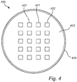
- FIG. 4 shows a top view of a light emitting module 400 comprising a plurality of light emitting diodes, here 20 individual LED chips, arranged on a board or support 403.
- the module comprises a plurality of first LED chips 401 adapted to emit light of the first wavelength range as defined herein, and at least one second LED chip 402 adapted to emit light of a second wavelength range as defined herein.
- the module 400 comprises a plurality of said second LED chips 402.
- a circular side wall 404 of a height exceeding the height of the LED chips 401, 402 is provided at the periphery of the board 403, enclosing the LED chips 401, 402, and may act as a support for a wavelength converting member which may be arranged as a lid or window, remotely from the LED chips 401, 402.
- Fig. 2 shows, a schematic side view of a similar arrangement, however without a side wall 404, and showing only two LED chips.
- the side wall 404 may have a reflective inner surface facing the LED chips 401, 402, thus forming a reflective light mixing chamber.
- a wavelength converting material may be provided directly on or in the vicinity of the individual LED chips 401, and optionally also the individual LED chip(s) 402.
- the LED chips 401, an optionally also LED chips 402 may be phosphor-converted, similar to Fig. 1 or Fig. 3a , respectively.
- a continuous layer of wavelength converting material may be applied over the LED chips 401 as well as the LED chips 402, similarly to the embodiment described with reference to Fig. 3b .
- the light emitting arrangement may comprise a plurality of said first light emitting elements and optionally also of said second light emitting elements. Different numbers of the respective first and second light emitting elements may be used in order to obtain a desired intensity ratio of the respective wavelength ranges emitted, in particular when all the light emitting elements are driven by the same current.
- the number of first light emitting elements to second light emitting element(s) may be from 10:1 to 3:2, in particular from 9:1 to 2:1, e.g. 9:1 to 3:1.
- the first LED chip may be a phosphor converted LED chip, based on a blue LED chip and a yellow or green or red phosphor.
- the second LED chip may be a phosphor-converted LED chip comprising a yellow or green or red phosphor.
- composition and/or the amount, concentration or layer thickness of the wavelength converting material(s) associated with the respective first and second LED chips may be the same or different.
- the light emitting diode may further comprise a red LED chip, typically a direct red LED chip (i.e. not comprising a phosphor).
- the light emitting module may include a scattering structure, e.g. added to a layer of wavelength converting material.
- a scattering structure may be applied on top of a layer of wavelength converting material, typically downstream thereof in the direction of light from the light emitting diode.
- a scattering structure may be integrated in the wavelength converting material, e.g. in the form of scattering particles or pores.
- Fig. 5 illustrates an embodiment of a light emitting module 10 according to embodiments of the present invention.
- the light emitting module 10 comprises an LED board 20 where two blue light emitting diodes 110 are arranged.
- the two blue light emitting diodes 110 are arranged to emit blue light having a peak wavelength between 440 and 460 nm.
- the two blue light emitting diodes 110 comprise a wavelength converting material 85, thus forming phosphor-converted LEDs, which may be adapted to emit white light depending on the choice of wavelength converting material. It is noted that any desired number of the LEDs 110, including a single LED 110, may be used.
- the light emitting module 10 further comprises a light emitting diode 120 arranged to emit short wavelength blue light having a peak wavelength between 400 and 440 nm.
- the light emitting module 10 comprises an optional direct red light emitting diode 90.
- the direct red light emitting diode 90 may emit light having a wavelength of > 600 nm. In this way the resulting white spectrum consists of two blue peaks, a broad yellow/green emission and a sharp red contribution.
- the at least one yellow/green/red phosphor converted blue light emitting diode may have a peak wavelength between 440 and 460 nm and the at least one secondary light emitting diode element may be arranged to emit short wavelength blue light having a peak wavelength between 400 and 440 nm.
- Fig. 6 illustrates another embodiment of a light emitting module 10 according to an embodiment of the present invention.
- the light emitting diode 120 arranged to emit short wavelength blue light does not comprise any phosphor.
- the module 10 comprises an optional direct red light emitting diode 90.
- the direct red light emitting diode 90 may emit light having a wavelength of >600 nm. It is noted that any desired number of the respective LEDs, including a single LED 110, may be used.
- the light emitting module 10 comprises two light emitting diodes 110 which are arranged to emit blue light having a peak wavelength between 440 and 460 nm.
- the light emitting module also comprises a light emitting diode 120 arranged to emit short wavelength blue light having a peak wavelength between 400 and 440 nm, and a direct red light emitting diode 90.
- the wavelength converting materials 35,85 are contained in a wavelength converting member provided as a remote phosphor element.
- the remote phosphor element comprises only wavelength converting material 35, and lacks wavelength converting material 85.
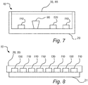
- Fig. 8 illustrates another embodiment of a light emitting module 10 comprising a LED board 21 where a number of light emitting diodes 110 are arranged closely together with a number of light emitting diodes 120.
- the LED board 100 of the light emitting module 10 comprises a yellow/green/red phosphor 35,85 directly applied onto it. This embodiment may be similar to the embodiment described with reference to Fig. 3b .
- the support 103, 203, 303 or the LED board 20 may be or form part of a chip-on-board structure.
- the yellow/green/red phosphor may be arranged on the light emitting diode board or in a remote configuration.
- the blue light emitting diodes may be positioned in a mixing box and the phosphor may be in the exit window.
- a method for generating light with a white light spectrum having a desired white rendition relating to an improved white appearance of a white object illuminated by a light emitting module may comprise the steps of arranging, in said light emitting module, at least one primary light emitting diode element to emit white light; arranging, in said light emitting module, at least one secondary light emitting diode element to emit short wavelength blue light.
- the method generates light with a white light spectrum having a desired white rendition relating to an improved white appearance of a white object illuminated by a light emitting module.
- the method comprises a step where at least one primary light emitting diode element is arranged in the light emitting module. In a subsequent step at least one secondary light emitting diode element is arranged in the light emitting module.
- a light emitting module according to embodiments of the invention may advantageously be used for illuminating objects and articles comprising a fluorescent whitening agent (FWA).
- FWA fluorescent whitening agent
- fluorescent whitening agents generally denotes chemical substances that upon excitation by UV light produce blue fluorescence usually with a peak at 445 nm. Fluorescent whitening agents are added to many products, for example paper, fabrics and plastics, in order to improve the white appearance. However, the present inventors have found that fluorescent whitening agents are also susceptible of excitation by short wavelength blue light, which leads to emission of regular blue light, thus contributing to improving the white impression of the illuminated material. In particular, light having a wavelength of 440 nm or lower, especially 420 nm or lower, can excite fluorescent whitening agents. In embodiments of the invention, a second light emitting diode having an emission peak wavelength in the range of from 400 to 440 nm may produce a sufficient intensity of light of ⁇ 420 nm to effectively excite a fluorescent whitening agent.
- a desirable "crisp white” effect may be represented by the difference (v' shift, ⁇ v' as seen in the 1976 CIE diagram) in color point of the light emitted/reflected by an object containing FWA compared to the light emitted by the light source used for illuminating said object.
- the color point of the emitted/reflected light (P2) is shifted further below the black body line compared to the color point of the light (P1) emitted by the light source, this may provide a crisp white effect ( Fig. 14 ). This phenomenon is explained in more detail with reference to Example 2 below.
- a ⁇ v' of at least -0.002 (- ⁇ v' ⁇ 0.002) may be sufficient, in particular where the color point of the light source is already below the BBL.
- a larger v' shift e.g. a ⁇ v' of at least -0.005, may be desirable.
- the inventors have found that the "crisp white” effect (e.g., a ⁇ v' of -0.005) obtained when illuminating an object containing a fluorescent whitening agent, using a light emitting module according to embodiments of the invention, is dependent on the intensity ratio of the "deep" blue light (e.g. 380-430 nm) to the total spectrum emitted by the module.
- the intensity ratio of the "deep" blue light e.g. 380-430 nm
- A' is equal to, or higher than, 0.6, typically at least 0.8, e.g. 0.8 ⁇ A' ⁇ 3. In embodiments of the invention, 1 ⁇ A' ⁇ 2.
- a graph plotting the calculated ⁇ v' as a function of A' is presented in Fig. 18 and described in more detail below (see Example 2).
- the first light emitting element used in the present invention (emitting "normal blue” light) has a peak wavelength in the range of from 440 to 460 nm, there will be some emitted light also below the peak wavelength and in order to better account for the total intensity of the light produced by the first light emitting element, the integral spectral power distribution is counted from 435 nm up to 465 nm. In embodiments of the invention, 0 ⁇ B ⁇ 0.15, i.e. the regular blue light forms less than 10 % of the total spectrum.
- a crisp white effect and color rendering index of at least 80 may be achieved.
- different numbers of the respective first and second light emitting elements may be used in order to obtain a desired intensity ratio, in particular when all the light emitting elements are driven by the same current.
- the number of first light emitting element to second light emitting elements may be from 2:1 to 4:1, in particular from 2:1 to 3:1, e.g. around 3:2.
- the number of first light emitting elements may be from 60 to 80, e.g. 72, and the number of second light emitting elements may be from 40 to 20, e.g. 28.
- Such a light emitting module may provide a ⁇ v' of at least -0.006, a CRI of at least 80, and a luminous flux of at least 2000 lm.
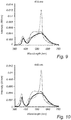
- a 455 nm blue emitting LED was used in combination with different selected phosphors in order to make white light.
- the green phosphors used were LuAG lumiramic, U821 (LuAG powder) and U822 (YAG powder).
- the green phosphors were combined with eCAS101, eCAS102 or a direct red LED chip.
- Fig. 9 various tested white spectra are shown for these different combinations, where these variations account for the different lines in the graph.
- a 445 nm blue emitting LED was used in combination with different selected yellow/green/red phosphors.
- Fig. 10 illustrates various white spectra for these corresponding combinations. Different phosphor choices are represented by the different lines in both Fig. 9 and Fig. 10 .
- cp color point
- Fig. 11 illustrates these variations in spectra for one of the combinations.
- Fig. 12 illustrates a white spectrum with an "excellent" white rendering (dashed line) compared with a white spectrum with an average white rendering (solid line).
- a light source comprising 20 normal blue LED chips and 5 deep blue LED chips, and a LuAG:Ce phosphor (U821) and a red phosphor (MCC BR101d) was used to illuminate a white fabric containing a fluorescent whitening agent.
- the color point of the light source was within the ANSI 3000 K bin.
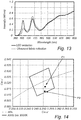
- the emission spectrum of the light source was measured, as well as the light reflected by the fabric. These spectra are shown in Fig. 13 . As can be seen, the light source spectrum(solid line) has a higher emission intensity peak at 410 nm, whereas the intensity of the light reflected or emitted by the fabric (dashed line) is lower at 410 nm but instead slightly higher in the wavelength range of roughly 420-480 nm.
- Fig. 14 the respective color points of the light from the light source and the fabric were recorded and are shown in Fig. 14 .
- the color point PI of the light emitted by the light source lies below the black body line.
- the color point P2 of the light emitted/reflected by the fabric is shifted further below the BBL and is therefore perceived as more white.
- the shift in the v' direction ( ⁇ v') is about - 0.004.
- Theoretical color points of the light from the light source and the fabric were calculated and are shown in Fig. 16 .
- the color point PI of the light emitted by the light source lies on the black body line, and within the ANSI bin 3000 K.
- the color point P2 of the light reflected by the fabric is shifted further below the BBL and lies on the border of or outside of the ANSI bin 3000 K, and is therefore perceived as more white.
- Fig. 17 shows an exemplary theoretical color point (P1) and acceptable color point space (dashed circle) for a light emitting module, and a resulting theoretical color point (P2) and desirable color point space (solid circle) for an FWA containing object illuminated by the light emitting module. Any color point within the dashed circle may be perceived as "crisp white”.
- the light source should preferably produce a ⁇ v' of at least -0.002 (- ⁇ v' ⁇ 0.002).
- light sources having a deep blue peak wavelength of 420 nm or lower may be preferred.
- Relatively high intensity ratios of short wavelength blue light may give satisfactory result with respect to "crisp white" effect. However, for reasons of efficiency and/or to maintain sufficiently high CRI, it may be preferable to use a relatively low ratio of short wavelength blue light to the total output light.
- Fig. 18 is a graph showing the expected ⁇ v' as a function of A', based on earlier experiments (illuminating a white fabric or paper using a light source according to embodiments of the invention).
- a ratio A' of 0.6 may result in a ⁇ v' of -0.002.
- the light emitting arrangement described herein may form part of a light emitting module for use in various lighting applications.
- a light emitting module may be used in a white light source, for example a spotlight or a luminaire, for illuminating objects e.g. in retail or exposition environments.
- the light emitting module according to embodiments of the invention typically comprised in a spotlight, may advantageously be used for accent lighting in retail environments.
- Fig. 19 illustrates an alternative embodiment of a light emitting arrangement 190 which uses only one type of light emitting element, notably a deep blue emitting LED chip 192 arranged on a substrate 103.
- a blue wavelength converting material 193 is provided to convert part of the deep blue light emitted by the chip 192 into normal blue light.
- a wavelength converting material 194 capable of converting normal blue light into light of the green to red wavelength range is provided remotely from the LED chip 192 and the blue wavelength converting material 193, although it is contemplated that the wavelength converting material 194 may also be located in the vicinity of or directly on the blue wavelength converting material 193. Similarly, the blue wavelength converting material 193 may also be located further away from the LED chip 192, however the wavelength converting material 194 may advantageously be provided downstream of the blue wavelength converting material 193 in the path of light.
Landscapes
- Engineering & Computer Science (AREA)
- Microelectronics & Electronic Packaging (AREA)
- Power Engineering (AREA)
- Physics & Mathematics (AREA)
- Computer Hardware Design (AREA)
- Optics & Photonics (AREA)
- General Engineering & Computer Science (AREA)
- Manufacturing & Machinery (AREA)
- Condensed Matter Physics & Semiconductors (AREA)
- General Physics & Mathematics (AREA)
- Led Device Packages (AREA)
- Non-Portable Lighting Devices Or Systems Thereof (AREA)
- Luminescent Compositions (AREA)
Claims (15)
- Lichtemittierendes Modul (100, 200, 300, 310, 400, 10), das angepasst ist, um weißes Ausgangslicht, das eine Emissionsspitze im Wellenlängenbereich von 400 bis 440 nm aufweist, zu erzeugen, umfassend:- mindestens ein erstes lichtemittierendes Element (101, 201, 301, 401, 110), das geeignet ist, Licht, das eine Emissionsspitze in einem ersten Wellenlängenbereich von 440 bis 460 nm aufweist, zu emittieren;- mindestens ein Wellenlängenumwandlungsmaterial (104, 204, 304, 306, 35, 85), das angeordnet ist, um Licht zu empfangen, das von dem ersten lichtemittierenden Element emittiert wird, und das in der Lage ist, Licht, das eine Emissionsspitze im grünen bis roten Wellenlängenbereich aufweist, zu emittieren; und- mindestens ein zweites lichtemittierendes Element (102, 202, 302, 402, 120), das angepasst ist, um Licht zu emittieren, das eine Emissionsspitze in einem zweiten Wellenlängenbereich von 400 bis 440 nm aufweist,wobei das lichtemittierende Modul angepasst ist, um ein Verhältnis B der integralen spektralen Leistungsverteilung E(λ) des Wellenlängenbereichs von 435 bis 465 nm zur integralen spektralen Leistungsverteilung des von dem lichtemittierenden Modul emittierten Gesamtspektrums zu erzeugen, definiert als

- Lichtemittierendes Modul (100, 200, 300, 310, 400, 10, 190) nach Anspruch 1, wobei das lichtemittierende Modul weiter angepasst ist, um ein Verhältnis A' der integralen spektralen Leistungsverteilung von Licht des Wellenlängenbereichs von 380 bis 430 nm zur integralen spektralen Leistungsverteilung des von dem lichtemittierenden Modul erzeugten Gesamtleistungslichts zu erzeugen, definiert als

- Lichtemittierendes Modul (100, 200, 300, 310, 400, 10, 190) nach Anspruch 1 oder 2, wobei der zweite Wellenlängenbereich von 405 bis 425 nm beträgt.
- Lichtemittierendes Modul (100, 200, 300, 310, 400, 10, 190) nach Anspruch 1 oder 2, umfassend mindestens zwei verschiedene Wellenlängenumwandlungsmaterialien.
- Lichtemittierendes Modul (100, 200, 300, 310, 400, 10, 190) nach Anspruch 1 oder 2, wobei ein Hauptabschnitt des von dem zweiten lichtemittierenden Element emittierten Lichts nicht durch das Wellenlängenumwandlungsmaterial (104, 204, 304, 305, 306, 35, 85, 194) umgewandelt wird.
- Lichtemittierendes Modul (190) nach einem der vorstehenden Ansprüche, wobei der zweite Wellenlängenbereich von 400 bis 420 nm beträgt.
- Lichtemittierendes Modul (100, 200, 300, 310, 400, 10, 190) nach Anspruch 1 oder 2, wobei das Wellenlängenumwandlungsmaterial eine Absorptionsspitzenwellenlänge von mehr als 440 nm aufweist.
- Lichtemittierendes Modul (100, 200, 300, 310, 400, 10, 190) nach Anspruch 1 oder 2, wobei das Wellenlängenumwandlungsmaterial ein cerdotierter Granat ist.
- Lichtemittierendes Modul (100, 200, 300, 310, 400, 10) nach Anspruch 1, umfassend eine Vielzahl des ersten lichtemittierenden Elements und optional eine Vielzahl des zweiten lichtemittierenden Elements, und wobei das Zahlenverhältnis der ersten lichtemittierenden Elemente zu dem/den zweiten lichtemittierenden Element(en) 10:1 bis 2:1 beträgt.
- Lichtemittierendes Modul (100, 200, 300, 310, 400, 10) nach Anspruch 1, wobei 1 ≤ A' ≤ 2.
- Lichtemittierendes Modul (200, 400, 10, 190) nach Anspruch 1 oder 2, wobei das Wellenlängenumwandlungsmaterial (204, 35, 85, 194) ein entferntes Leuchtstoffelement ist.
- Lichtemittierendes Modul (100, 300, 310, 400, 10) nach Anspruch 1, wobei mindestens ein Abschnitt des Wellenlängenumwandlungsmaterials (104, 304, 306, 35, 85) auf dem ersten lichtemittierenden Element bereitgestellt ist und eine Weißlicht-Leuchtstoffkonversions-LED bildet.
- Verfahren zur Erzeugung von Weißlicht unter Verwendung eines lichtemittierenden Moduls nach Anspruch 1 oder 2, umfassend das Betreiben mindestens des ersten und zweiten lichtemittierenden Elements, um ein Verhältnis B der integralen spektralen Leistungsverteilung E(λ) des Wellenlängenbereichs von 435 bis 465 nm zur integralen spektralen Leistungsverteilung des von dem Modul emittierten Gesamtspektrums zu erzeugen, definiert als

- Verwendung eines lichtemittierenden Moduls nach Anspruch 1 oder 2 zum Beleuchten eines Objekts, umfassend ein fluoreszierendes Aufhellungsmittel.
- Lampe, Strahler oder Leuchte umfassend mindestens ein lichtemittierendes Modul nach Anspruch 1 oder 2.
Applications Claiming Priority (5)
| Application Number | Priority Date | Filing Date | Title |
|---|---|---|---|
| US201261621046P | 2012-04-06 | 2012-04-06 | |
| EP12163539.5A EP2650918A1 (de) | 2012-04-10 | 2012-04-10 | Lichtemittierendes Modul |
| EP13159589 | 2013-03-15 | ||
| EP13724395.2A EP2834842B1 (de) | 2012-04-06 | 2013-04-04 | Weisslicht emittierendes modul |
| PCT/IB2013/052681 WO2013150470A1 (en) | 2012-04-06 | 2013-04-04 | White light emitting module |
Related Parent Applications (2)
| Application Number | Title | Priority Date | Filing Date |
|---|---|---|---|
| EP13724395.2A Division EP2834842B1 (de) | 2012-04-06 | 2013-04-04 | Weisslicht emittierendes modul |
| EP13724395.2A Division-Into EP2834842B1 (de) | 2012-04-06 | 2013-04-04 | Weisslicht emittierendes modul |
Publications (2)
| Publication Number | Publication Date |
|---|---|
| EP3382755A1 EP3382755A1 (de) | 2018-10-03 |
| EP3382755B1 true EP3382755B1 (de) | 2020-01-08 |
Family
ID=49300071
Family Applications (2)
| Application Number | Title | Priority Date | Filing Date |
|---|---|---|---|
| EP18167770.9A Active EP3382755B1 (de) | 2012-04-06 | 2013-04-04 | Weisslicht emittierendes modul |
| EP13724395.2A Active EP2834842B1 (de) | 2012-04-06 | 2013-04-04 | Weisslicht emittierendes modul |
Family Applications After (1)
| Application Number | Title | Priority Date | Filing Date |
|---|---|---|---|
| EP13724395.2A Active EP2834842B1 (de) | 2012-04-06 | 2013-04-04 | Weisslicht emittierendes modul |
Country Status (6)
| Country | Link |
|---|---|
| US (1) | US10090442B2 (de) |
| EP (2) | EP3382755B1 (de) |
| JP (1) | JP6363061B2 (de) |
| CN (1) | CN104303298B (de) |
| RU (1) | RU2623682C2 (de) |
| WO (1) | WO2013150470A1 (de) |
Families Citing this family (47)
| Publication number | Priority date | Publication date | Assignee | Title |
|---|---|---|---|---|
| DE202007019100U1 (de) * | 2007-09-12 | 2010-09-02 | Lumitech Produktion Und Entwicklung Gmbh | LED-Modul, LED-Leuchtmittel und LED-Leuchte für die energieeffiziente Wiedergabe von weißem Licht |
| TWM458672U (zh) * | 2013-04-10 | 2013-08-01 | Genesis Photonics Inc | 光源模組 |
| EP3064039B1 (de) * | 2013-10-28 | 2020-05-13 | GE Lighting Solutions, LLC | Lampen für verbesserte optische aufhellung und farbpräferenz |
| US10334686B2 (en) * | 2014-02-21 | 2019-06-25 | Signify Holding B.V. | Light emitting module, a lamp, a luminaire and a method of illuminating an object |
| CN103839935A (zh) * | 2014-03-14 | 2014-06-04 | 无锡实益达电子有限公司 | 一种具有高色彩表现能力的集成式白光led光源 |
| US9923126B2 (en) | 2014-04-30 | 2018-03-20 | Sharp Kabushiki Kaisha | Light emitting device having high color rendering using three phosphor types |
| EP3155874B1 (de) * | 2014-06-10 | 2020-05-13 | Signify Holding B.V. | Anordnung zur lichtabgabe mit einstellbarem emissionsspektrum |
| CN106574175B (zh) | 2014-09-11 | 2018-08-07 | 飞利浦照明控股有限公司 | 具有加强的白色显现和转换效率的pc-led模块 |
| TW201616682A (zh) | 2014-10-24 | 2016-05-01 | Edison Opto Corp | 光線發射裝置 |
| US10424562B2 (en) * | 2014-12-16 | 2019-09-24 | Citizen Electronics Co., Ltd. | Light emitting device with phosphors |
| JP6501803B2 (ja) * | 2015-02-13 | 2019-04-17 | シャープ株式会社 | 光源装置および発光装置 |
| WO2016159141A1 (ja) | 2015-04-03 | 2016-10-06 | シャープ株式会社 | 発光装置 |
| JP2017017059A (ja) * | 2015-06-26 | 2017-01-19 | パナソニックIpマネジメント株式会社 | 照明用光源及び照明装置 |
| US20170014538A1 (en) * | 2015-07-14 | 2017-01-19 | Juha Rantala | LED structure and luminaire for continuous disinfection |
| US11273324B2 (en) * | 2015-07-14 | 2022-03-15 | Illumipure Corp | LED structure and luminaire for continuous disinfection |
| US10918747B2 (en) | 2015-07-30 | 2021-02-16 | Vital Vio, Inc. | Disinfecting lighting device |
| EP3368634B1 (de) | 2015-10-29 | 2019-12-11 | Signify Holding B.V. | Verbesserte weissbeleuchtungsvorrichtung für einzelhandelsbeleuchtung |
| JP7221052B2 (ja) * | 2016-04-29 | 2023-02-13 | ルミレッズ ホールディング ベーフェー | 高輝度明白色led光源 |
| JP6735471B2 (ja) * | 2016-06-24 | 2020-08-05 | パナソニックIpマネジメント株式会社 | 発光装置、浴光方法及び発光システム |
| JP6783985B2 (ja) * | 2016-09-29 | 2020-11-11 | 豊田合成株式会社 | 発光装置 |
| US10030839B2 (en) | 2016-11-16 | 2018-07-24 | Amsterdam Printing & Litho, Inc. | Backlit, laser engraved metalized promotional items |
| JP7053980B2 (ja) * | 2016-11-16 | 2022-04-13 | 日亜化学工業株式会社 | 発光装置 |
| JP6944104B2 (ja) | 2016-11-30 | 2021-10-06 | 日亜化学工業株式会社 | 発光装置 |
| US10422501B2 (en) * | 2016-12-14 | 2019-09-24 | Ford Global Technologies, Llc | Vehicle lighting assembly |
| CN110402494A (zh) * | 2017-01-13 | 2019-11-01 | 尤哈·兰塔拉 | 用于持续消毒的led结构和照明器 |
| FR3062459B1 (fr) * | 2017-02-01 | 2021-03-19 | Schneider Electric Ind Sas | Dispositif a fonction de signalisation lumineuse |
| WO2018184575A1 (zh) * | 2017-04-07 | 2018-10-11 | 苏州欧普照明有限公司 | 一种光源模组及包括该光源模组的照明装置 |
| WO2018202534A1 (en) | 2017-05-02 | 2018-11-08 | Philips Lighting Holding B.V. | Warm white led spectrum especially for retail applications |
| KR102430098B1 (ko) * | 2017-06-15 | 2022-08-05 | 쑤저우 레킨 세미컨덕터 컴퍼니 리미티드 | 조명 모듈 |
| JP7086185B2 (ja) | 2017-10-19 | 2022-06-17 | シグニファイ ホールディング ビー ヴィ | 投影照明のための増強された白色光 |
| CN108183099B (zh) * | 2017-12-21 | 2021-06-15 | 厦门市三安光电科技有限公司 | 一种白光led封装结构以及白光源系统 |
| US10413626B1 (en) * | 2018-03-29 | 2019-09-17 | Vital Vio, Inc. | Multiple light emitter for inactivating microorganisms |
| US10529900B2 (en) * | 2018-05-05 | 2020-01-07 | Ideal Industries Lighting Llc | Solid state lighting device providing spectral power distribution with enhanced perceived brightness |
| US10788709B2 (en) * | 2018-10-30 | 2020-09-29 | Innolux Corporation | Lighting device |
| US20200161510A1 (en) * | 2018-11-19 | 2020-05-21 | Seoul Viosys Co., Ltd. | Led lighting apparatus having sterilizing function |
| EP3892068A1 (de) | 2018-12-04 | 2021-10-13 | Signify Holding B.V. | Crisp-weissabstimmung |
| CN113544432A (zh) * | 2019-01-18 | 2021-10-22 | 研究发展中心“拜鲁门”有限责任公司 | 具有生物辐射光谱的led白光源 |
| CN110212076B (zh) * | 2019-06-05 | 2024-03-19 | 欧普照明股份有限公司 | 一种光源模组及包括该光源模组的照明装置 |
| US11541135B2 (en) | 2019-06-28 | 2023-01-03 | Vyv, Inc. | Multiple band visible light disinfection |
| CN112242411B (zh) * | 2019-07-16 | 2024-09-03 | 群创光电股份有限公司 | 显示装置 |
| JP7270044B2 (ja) * | 2019-08-07 | 2023-05-09 | 京セラ株式会社 | 照明装置 |
| US11369704B2 (en) | 2019-08-15 | 2022-06-28 | Vyv, Inc. | Devices configured to disinfect interiors |
| US11878084B2 (en) | 2019-09-20 | 2024-01-23 | Vyv, Inc. | Disinfecting light emitting subcomponent |
| US11499707B2 (en) | 2020-04-13 | 2022-11-15 | Calyxpure, Inc. | Light fixture having a fan and ultraviolet sterilization functionality |
| TWI728873B (zh) * | 2020-07-21 | 2021-05-21 | 隆達電子股份有限公司 | 發光二極體裝置 |
| CN111828883A (zh) * | 2020-08-14 | 2020-10-27 | 贵州西能电光科技发展有限公司 | 一种led白光发光系统 |
| US11759540B2 (en) | 2021-05-11 | 2023-09-19 | Calyxpure, Inc. | Portable disinfection unit |
Family Cites Families (32)
| Publication number | Priority date | Publication date | Assignee | Title |
|---|---|---|---|---|
| US6893473B2 (en) * | 2002-05-07 | 2005-05-17 | Weyerhaeuser.Company | Whitened fluff pulp |
| TW200512949A (en) | 2003-09-17 | 2005-04-01 | Nanya Plastics Corp | A method to provide emission of white color light by the principle of secondary excitation and its product |
| US6942360B2 (en) * | 2003-10-01 | 2005-09-13 | Enertron, Inc. | Methods and apparatus for an LED light engine |
| CN100470117C (zh) * | 2003-10-01 | 2009-03-18 | 恩纳特隆公司 | 发光二极管发光板的方法和装置 |
| TWI263356B (en) * | 2003-11-27 | 2006-10-01 | Kuen-Juei Li | Light-emitting device |
| US7066623B2 (en) | 2003-12-19 | 2006-06-27 | Soo Ghee Lee | Method and apparatus for producing untainted white light using off-white light emitting diodes |
| KR100655894B1 (ko) * | 2004-05-06 | 2006-12-08 | 서울옵토디바이스주식회사 | 색온도 및 연색성이 우수한 파장변환 발광장치 |
| KR100658700B1 (ko) | 2004-05-13 | 2006-12-15 | 서울옵토디바이스주식회사 | Rgb 발광소자와 형광체를 조합한 발광장치 |
| JP5616000B2 (ja) * | 2004-12-06 | 2014-10-29 | コーニンクレッカ フィリップス エヌ ヴェ | コンパクトな色可変光源としてのシングルチップled |
| WO2006105649A1 (en) | 2005-04-06 | 2006-10-12 | Tir Systems Ltd. | White light luminaire with adjustable correlated colour temperature |
| US7329951B2 (en) | 2005-04-27 | 2008-02-12 | International Business Machines Corporation | Solder bumps in flip-chip technologies |
| DE102005036398A1 (de) | 2005-08-03 | 2007-02-15 | Khs Ag | Vorrichtung zum Aufbringen von Banderolen |
| WO2007069142A2 (en) * | 2005-12-14 | 2007-06-21 | Philips Intellectual Property & Standards Gmbh | Light-emitting device |
| US8174032B2 (en) * | 2006-03-16 | 2012-05-08 | Light Engines Corporation | Semiconductor white light sources |
| JP2008010470A (ja) * | 2006-06-27 | 2008-01-17 | Mitsubishi Chemicals Corp | 照明装置 |
| JP4989936B2 (ja) * | 2006-07-27 | 2012-08-01 | 株式会社朝日ラバー | 照明装置 |
| JP5029203B2 (ja) | 2006-08-11 | 2012-09-19 | 三菱化学株式会社 | 照明装置 |
| WO2008075260A2 (en) | 2006-12-18 | 2008-06-26 | Koninklijke Philips Electronics N.V. | Light source and method for operating a lighting system |
| WO2008101156A2 (en) * | 2007-02-15 | 2008-08-21 | Lighting Science Group Corporation | High color rendering index white led light system using multi-wavelength pump sources and mixed phosphors |
| US8410714B2 (en) | 2007-11-12 | 2013-04-02 | Mitsubishi Chemical Corporation | Illuminating device |
| RU2525834C2 (ru) * | 2008-01-22 | 2014-08-20 | Конинклейке Филипс Электроникс Н.В. | Осветительное устройство с сид и передающим основанием, включающим люминесцентный материал |
| US20100244731A1 (en) | 2008-02-13 | 2010-09-30 | Canon Components, Inc. | White light emitting diode, white light emitting apparatus, and linear illuminator using the same |
| EP2247891B1 (de) * | 2008-02-21 | 2019-06-05 | Signify Holding B.V. | Glühlampenähnliche led-lichtquelle |
| US8567973B2 (en) * | 2008-03-07 | 2013-10-29 | Intematix Corporation | Multiple-chip excitation systems for white light emitting diodes (LEDs) |
| JP5239442B2 (ja) * | 2008-03-25 | 2013-07-17 | コニカミノルタオプティクス株式会社 | 蛍光試料の光学特性測定方法および装置 |
| DE102008050643B4 (de) | 2008-10-07 | 2022-11-03 | OSRAM Opto Semiconductors Gesellschaft mit beschränkter Haftung | Leuchtmittel |
| JP2010238492A (ja) * | 2009-03-31 | 2010-10-21 | Panasonic Corp | 照明装置 |
| JP2011059809A (ja) | 2009-09-07 | 2011-03-24 | Toshiba Corp | 監視装置 |
| JP2011159809A (ja) * | 2010-02-01 | 2011-08-18 | Mitsubishi Chemicals Corp | 白色発光装置 |
| US8508127B2 (en) | 2010-03-09 | 2013-08-13 | Cree, Inc. | High CRI lighting device with added long-wavelength blue color |
| DE202011000007U1 (de) * | 2011-01-04 | 2012-04-05 | Zumtobel Lighting Gmbh | LED-Anordnung zur Erzeugung von weißem Licht |
| JP5325959B2 (ja) * | 2011-03-09 | 2013-10-23 | 株式会社東芝 | 蛍光体およびそれを用いた発光装置 |
-
2013
- 2013-04-04 EP EP18167770.9A patent/EP3382755B1/de active Active
- 2013-04-04 EP EP13724395.2A patent/EP2834842B1/de active Active
- 2013-04-04 WO PCT/IB2013/052681 patent/WO2013150470A1/en active Application Filing
- 2013-04-04 JP JP2015503977A patent/JP6363061B2/ja active Active
- 2013-04-04 RU RU2014144678A patent/RU2623682C2/ru active
- 2013-04-04 US US14/390,439 patent/US10090442B2/en active Active
- 2013-04-04 CN CN201380018703.0A patent/CN104303298B/zh active Active
Non-Patent Citations (1)
| Title |
|---|
| None * |
Also Published As
| Publication number | Publication date |
|---|---|
| RU2623682C2 (ru) | 2017-06-28 |
| US10090442B2 (en) | 2018-10-02 |
| US20150049459A1 (en) | 2015-02-19 |
| CN104303298B (zh) | 2018-01-19 |
| CN104303298A (zh) | 2015-01-21 |
| RU2014144678A (ru) | 2016-05-27 |
| EP2834842A1 (de) | 2015-02-11 |
| EP3382755A1 (de) | 2018-10-03 |
| WO2013150470A1 (en) | 2013-10-10 |
| JP6363061B2 (ja) | 2018-07-25 |
| EP2834842B1 (de) | 2018-07-04 |
| JP2015515133A (ja) | 2015-05-21 |
Similar Documents
| Publication | Publication Date | Title |
|---|---|---|
| EP3382755B1 (de) | Weisslicht emittierendes modul | |
| EP3008374B1 (de) | Lichtemittierende anordnung mit angepasster ausgangsspektrums | |
| JP4989936B2 (ja) | 照明装置 | |
| US8747697B2 (en) | Gallium-substituted yttrium aluminum garnet phosphor and light emitting devices including the same | |
| TWI394818B (zh) | 包含缺色補償發光材料的發光系統 | |
| US10074781B2 (en) | Semiconductor light emitting devices including multiple red phosphors that exhibit good color rendering properties with increased brightness | |
| US20140167601A1 (en) | Enhanced Luminous Flux Semiconductor Light Emitting Devices Including Red Phosphors that Exhibit Good Color Rendering Properties and Related Red Phosphors | |
| CN108350354B (zh) | 用于零售照明的改进的白色照明设备 | |
| JP6275829B2 (ja) | 発光装置 | |
| US9219202B2 (en) | Semiconductor light emitting devices including red phosphors that exhibit good color rendering properties and related red phosphors | |
| WO2014203841A1 (ja) | 発光装置 | |
| US10374133B2 (en) | Light emitting apparatus with two primary lighting peaks | |
| US10658552B2 (en) | Blue emitting phosphor converted LED with blue pigment | |
| US7059927B2 (en) | Method for manufacturing white light source | |
| JP6354607B2 (ja) | 発光装置 | |
| KR20150143916A (ko) | 고연색성 백색 발광 소자 | |
| KR20180021748A (ko) | 고연색성 백색 발광 소자 | |
| KR101652258B1 (ko) | 고연색성 백색 발광 소자 | |
| KR101855391B1 (ko) | 고연색성 백색 발광 소자 | |
| CN205911309U (zh) | 发光模块以及照明装置 |
Legal Events
| Date | Code | Title | Description |
|---|---|---|---|
| PUAI | Public reference made under article 153(3) epc to a published international application that has entered the european phase |
Free format text: ORIGINAL CODE: 0009012 |
|
| STAA | Information on the status of an ep patent application or granted ep patent |
Free format text: STATUS: THE APPLICATION HAS BEEN PUBLISHED |
|
| AC | Divisional application: reference to earlier application |
Ref document number: 2834842 Country of ref document: EP Kind code of ref document: P |
|
| AK | Designated contracting states |
Kind code of ref document: A1 Designated state(s): AL AT BE BG CH CY CZ DE DK EE ES FI FR GB GR HR HU IE IS IT LI LT LU LV MC MK MT NL NO PL PT RO RS SE SI SK SM TR |
|
| RAP1 | Party data changed (applicant data changed or rights of an application transferred) |
Owner name: PHILIPS LIGHTING HOLDING B.V. |
|
| RAP1 | Party data changed (applicant data changed or rights of an application transferred) |
Owner name: SIGNIFY HOLDING B.V. |
|
| STAA | Information on the status of an ep patent application or granted ep patent |
Free format text: STATUS: REQUEST FOR EXAMINATION WAS MADE |
|
| 17P | Request for examination filed |
Effective date: 20190403 |
|
| RBV | Designated contracting states (corrected) |
Designated state(s): AL AT BE BG CH CY CZ DE DK EE ES FI FR GB GR HR HU IE IS IT LI LT LU LV MC MK MT NL NO PL PT RO RS SE SI SK SM TR |
|
| GRAP | Despatch of communication of intention to grant a patent |
Free format text: ORIGINAL CODE: EPIDOSNIGR1 |
|
| STAA | Information on the status of an ep patent application or granted ep patent |
Free format text: STATUS: GRANT OF PATENT IS INTENDED |
|
| RIC1 | Information provided on ipc code assigned before grant |
Ipc: H01L 33/50 20100101ALN20190725BHEP Ipc: F21K 9/64 20160101ALN20190725BHEP Ipc: F21K 99/00 20160101ALI20190725BHEP Ipc: H01L 25/075 20060101AFI20190725BHEP |
|
| INTG | Intention to grant announced |
Effective date: 20190808 |
|
| RIC1 | Information provided on ipc code assigned before grant |
Ipc: H01L 33/50 20100101ALN20190726BHEP Ipc: F21K 99/00 20160101ALI20190726BHEP Ipc: H01L 25/075 20060101AFI20190726BHEP Ipc: F21K 9/64 20160101ALN20190726BHEP |
|
| GRAS | Grant fee paid |
Free format text: ORIGINAL CODE: EPIDOSNIGR3 |
|
| GRAA | (expected) grant |
Free format text: ORIGINAL CODE: 0009210 |
|
| STAA | Information on the status of an ep patent application or granted ep patent |
Free format text: STATUS: THE PATENT HAS BEEN GRANTED |
|
| AC | Divisional application: reference to earlier application |
Ref document number: 2834842 Country of ref document: EP Kind code of ref document: P |
|
| AK | Designated contracting states |
Kind code of ref document: B1 Designated state(s): AL AT BE BG CH CY CZ DE DK EE ES FI FR GB GR HR HU IE IS IT LI LT LU LV MC MK MT NL NO PL PT RO RS SE SI SK SM TR |
|
| REG | Reference to a national code |
Ref country code: GB Ref legal event code: FG4D |
|
| REG | Reference to a national code |
Ref country code: CH Ref legal event code: EP |
|
| REG | Reference to a national code |
Ref country code: DE Ref legal event code: R096 Ref document number: 602013065034 Country of ref document: DE |
|
| REG | Reference to a national code |
Ref country code: IE Ref legal event code: FG4D |
|
| REG | Reference to a national code |
Ref country code: AT Ref legal event code: REF Ref document number: 1223748 Country of ref document: AT Kind code of ref document: T Effective date: 20200215 |
|
| REG | Reference to a national code |
Ref country code: NL Ref legal event code: FP |
|
| REG | Reference to a national code |
Ref country code: LT Ref legal event code: MG4D |
|
| PG25 | Lapsed in a contracting state [announced via postgrant information from national office to epo] |
Ref country code: NO Free format text: LAPSE BECAUSE OF FAILURE TO SUBMIT A TRANSLATION OF THE DESCRIPTION OR TO PAY THE FEE WITHIN THE PRESCRIBED TIME-LIMIT Effective date: 20200408 Ref country code: LT Free format text: LAPSE BECAUSE OF FAILURE TO SUBMIT A TRANSLATION OF THE DESCRIPTION OR TO PAY THE FEE WITHIN THE PRESCRIBED TIME-LIMIT Effective date: 20200108 Ref country code: PT Free format text: LAPSE BECAUSE OF FAILURE TO SUBMIT A TRANSLATION OF THE DESCRIPTION OR TO PAY THE FEE WITHIN THE PRESCRIBED TIME-LIMIT Effective date: 20200531 Ref country code: RS Free format text: LAPSE BECAUSE OF FAILURE TO SUBMIT A TRANSLATION OF THE DESCRIPTION OR TO PAY THE FEE WITHIN THE PRESCRIBED TIME-LIMIT Effective date: 20200108 Ref country code: FI Free format text: LAPSE BECAUSE OF FAILURE TO SUBMIT A TRANSLATION OF THE DESCRIPTION OR TO PAY THE FEE WITHIN THE PRESCRIBED TIME-LIMIT Effective date: 20200108 |
|
| PG25 | Lapsed in a contracting state [announced via postgrant information from national office to epo] |
Ref country code: GR Free format text: LAPSE BECAUSE OF FAILURE TO SUBMIT A TRANSLATION OF THE DESCRIPTION OR TO PAY THE FEE WITHIN THE PRESCRIBED TIME-LIMIT Effective date: 20200409 Ref country code: HR Free format text: LAPSE BECAUSE OF FAILURE TO SUBMIT A TRANSLATION OF THE DESCRIPTION OR TO PAY THE FEE WITHIN THE PRESCRIBED TIME-LIMIT Effective date: 20200108 Ref country code: BG Free format text: LAPSE BECAUSE OF FAILURE TO SUBMIT A TRANSLATION OF THE DESCRIPTION OR TO PAY THE FEE WITHIN THE PRESCRIBED TIME-LIMIT Effective date: 20200408 Ref country code: SE Free format text: LAPSE BECAUSE OF FAILURE TO SUBMIT A TRANSLATION OF THE DESCRIPTION OR TO PAY THE FEE WITHIN THE PRESCRIBED TIME-LIMIT Effective date: 20200108 Ref country code: LV Free format text: LAPSE BECAUSE OF FAILURE TO SUBMIT A TRANSLATION OF THE DESCRIPTION OR TO PAY THE FEE WITHIN THE PRESCRIBED TIME-LIMIT Effective date: 20200108 Ref country code: IS Free format text: LAPSE BECAUSE OF FAILURE TO SUBMIT A TRANSLATION OF THE DESCRIPTION OR TO PAY THE FEE WITHIN THE PRESCRIBED TIME-LIMIT Effective date: 20200508 |
|
| REG | Reference to a national code |
Ref country code: DE Ref legal event code: R097 Ref document number: 602013065034 Country of ref document: DE |
|
| PG25 | Lapsed in a contracting state [announced via postgrant information from national office to epo] |
Ref country code: CZ Free format text: LAPSE BECAUSE OF FAILURE TO SUBMIT A TRANSLATION OF THE DESCRIPTION OR TO PAY THE FEE WITHIN THE PRESCRIBED TIME-LIMIT Effective date: 20200108 Ref country code: RO Free format text: LAPSE BECAUSE OF FAILURE TO SUBMIT A TRANSLATION OF THE DESCRIPTION OR TO PAY THE FEE WITHIN THE PRESCRIBED TIME-LIMIT Effective date: 20200108 Ref country code: EE Free format text: LAPSE BECAUSE OF FAILURE TO SUBMIT A TRANSLATION OF THE DESCRIPTION OR TO PAY THE FEE WITHIN THE PRESCRIBED TIME-LIMIT Effective date: 20200108 Ref country code: SM Free format text: LAPSE BECAUSE OF FAILURE TO SUBMIT A TRANSLATION OF THE DESCRIPTION OR TO PAY THE FEE WITHIN THE PRESCRIBED TIME-LIMIT Effective date: 20200108 Ref country code: DK Free format text: LAPSE BECAUSE OF FAILURE TO SUBMIT A TRANSLATION OF THE DESCRIPTION OR TO PAY THE FEE WITHIN THE PRESCRIBED TIME-LIMIT Effective date: 20200108 Ref country code: ES Free format text: LAPSE BECAUSE OF FAILURE TO SUBMIT A TRANSLATION OF THE DESCRIPTION OR TO PAY THE FEE WITHIN THE PRESCRIBED TIME-LIMIT Effective date: 20200108 Ref country code: SK Free format text: LAPSE BECAUSE OF FAILURE TO SUBMIT A TRANSLATION OF THE DESCRIPTION OR TO PAY THE FEE WITHIN THE PRESCRIBED TIME-LIMIT Effective date: 20200108 |
|
| PLBE | No opposition filed within time limit |
Free format text: ORIGINAL CODE: 0009261 |
|
| STAA | Information on the status of an ep patent application or granted ep patent |
Free format text: STATUS: NO OPPOSITION FILED WITHIN TIME LIMIT |
|
| PG25 | Lapsed in a contracting state [announced via postgrant information from national office to epo] |
Ref country code: MC Free format text: LAPSE BECAUSE OF FAILURE TO SUBMIT A TRANSLATION OF THE DESCRIPTION OR TO PAY THE FEE WITHIN THE PRESCRIBED TIME-LIMIT Effective date: 20200108 |
|
| REG | Reference to a national code |
Ref country code: CH Ref legal event code: PL |
|
| 26N | No opposition filed |
Effective date: 20201009 |
|
| PG25 | Lapsed in a contracting state [announced via postgrant information from national office to epo] |
Ref country code: CH Free format text: LAPSE BECAUSE OF NON-PAYMENT OF DUE FEES Effective date: 20200430 Ref country code: LU Free format text: LAPSE BECAUSE OF NON-PAYMENT OF DUE FEES Effective date: 20200404 Ref country code: LI Free format text: LAPSE BECAUSE OF NON-PAYMENT OF DUE FEES Effective date: 20200430 Ref country code: IT Free format text: LAPSE BECAUSE OF FAILURE TO SUBMIT A TRANSLATION OF THE DESCRIPTION OR TO PAY THE FEE WITHIN THE PRESCRIBED TIME-LIMIT Effective date: 20200108 |
|
| REG | Reference to a national code |
Ref country code: BE Ref legal event code: MM Effective date: 20200430 |
|
| PG25 | Lapsed in a contracting state [announced via postgrant information from national office to epo] |
Ref country code: PL Free format text: LAPSE BECAUSE OF FAILURE TO SUBMIT A TRANSLATION OF THE DESCRIPTION OR TO PAY THE FEE WITHIN THE PRESCRIBED TIME-LIMIT Effective date: 20200108 Ref country code: BE Free format text: LAPSE BECAUSE OF NON-PAYMENT OF DUE FEES Effective date: 20200430 Ref country code: SI Free format text: LAPSE BECAUSE OF FAILURE TO SUBMIT A TRANSLATION OF THE DESCRIPTION OR TO PAY THE FEE WITHIN THE PRESCRIBED TIME-LIMIT Effective date: 20200108 |
|
| PG25 | Lapsed in a contracting state [announced via postgrant information from national office to epo] |
Ref country code: IE Free format text: LAPSE BECAUSE OF NON-PAYMENT OF DUE FEES Effective date: 20200404 |
|
| REG | Reference to a national code |
Ref country code: AT Ref legal event code: UEP Ref document number: 1223748 Country of ref document: AT Kind code of ref document: T Effective date: 20200108 |
|
| PG25 | Lapsed in a contracting state [announced via postgrant information from national office to epo] |
Ref country code: TR Free format text: LAPSE BECAUSE OF FAILURE TO SUBMIT A TRANSLATION OF THE DESCRIPTION OR TO PAY THE FEE WITHIN THE PRESCRIBED TIME-LIMIT Effective date: 20200108 Ref country code: MT Free format text: LAPSE BECAUSE OF FAILURE TO SUBMIT A TRANSLATION OF THE DESCRIPTION OR TO PAY THE FEE WITHIN THE PRESCRIBED TIME-LIMIT Effective date: 20200108 Ref country code: CY Free format text: LAPSE BECAUSE OF FAILURE TO SUBMIT A TRANSLATION OF THE DESCRIPTION OR TO PAY THE FEE WITHIN THE PRESCRIBED TIME-LIMIT Effective date: 20200108 |
|
| PG25 | Lapsed in a contracting state [announced via postgrant information from national office to epo] |
Ref country code: MK Free format text: LAPSE BECAUSE OF FAILURE TO SUBMIT A TRANSLATION OF THE DESCRIPTION OR TO PAY THE FEE WITHIN THE PRESCRIBED TIME-LIMIT Effective date: 20200108 Ref country code: AL Free format text: LAPSE BECAUSE OF FAILURE TO SUBMIT A TRANSLATION OF THE DESCRIPTION OR TO PAY THE FEE WITHIN THE PRESCRIBED TIME-LIMIT Effective date: 20200108 |
|
| P01 | Opt-out of the competence of the unified patent court (upc) registered |
Effective date: 20230421 |
|
| PGFP | Annual fee paid to national office [announced via postgrant information from national office to epo] |
Ref country code: NL Payment date: 20240425 Year of fee payment: 12 |
|
| PGFP | Annual fee paid to national office [announced via postgrant information from national office to epo] |
Ref country code: GB Payment date: 20240423 Year of fee payment: 12 |
|
| PGFP | Annual fee paid to national office [announced via postgrant information from national office to epo] |
Ref country code: DE Payment date: 20240627 Year of fee payment: 12 |
|
| PGFP | Annual fee paid to national office [announced via postgrant information from national office to epo] |
Ref country code: AT Payment date: 20240417 Year of fee payment: 12 |
|
| PGFP | Annual fee paid to national office [announced via postgrant information from national office to epo] |
Ref country code: FR Payment date: 20240430 Year of fee payment: 12 |