EP3352199B1 - Iii-n-basiertes substrat für leistungselektronische vorrichtungen und verfahren zur herstellung davon - Google Patents
Iii-n-basiertes substrat für leistungselektronische vorrichtungen und verfahren zur herstellung davon Download PDFInfo
- Publication number
- EP3352199B1 EP3352199B1 EP17202493.7A EP17202493A EP3352199B1 EP 3352199 B1 EP3352199 B1 EP 3352199B1 EP 17202493 A EP17202493 A EP 17202493A EP 3352199 B1 EP3352199 B1 EP 3352199B1
- Authority
- EP
- European Patent Office
- Prior art keywords
- superlattice
- laminate
- aluminum content
- layers
- iii
- Prior art date
- Legal status (The legal status is an assumption and is not a legal conclusion. Google has not performed a legal analysis and makes no representation as to the accuracy of the status listed.)
- Active
Links
Images




Classifications
-
- H—ELECTRICITY
- H10—SEMICONDUCTOR DEVICES; ELECTRIC SOLID-STATE DEVICES NOT OTHERWISE PROVIDED FOR
- H10D—INORGANIC ELECTRIC SEMICONDUCTOR DEVICES
- H10D62/00—Semiconductor bodies, or regions thereof, of devices having potential barriers
- H10D62/80—Semiconductor bodies, or regions thereof, of devices having potential barriers characterised by the materials
- H10D62/81—Semiconductor bodies, or regions thereof, of devices having potential barriers characterised by the materials of structures exhibiting quantum-confinement effects, e.g. single quantum wells; of structures having periodic or quasi-periodic potential variation
- H10D62/815—Semiconductor bodies, or regions thereof, of devices having potential barriers characterised by the materials of structures exhibiting quantum-confinement effects, e.g. single quantum wells; of structures having periodic or quasi-periodic potential variation of structures having periodic or quasi-periodic potential variation, e.g. superlattices or multiple quantum wells [MQW]
- H10D62/8161—Semiconductor bodies, or regions thereof, of devices having potential barriers characterised by the materials of structures exhibiting quantum-confinement effects, e.g. single quantum wells; of structures having periodic or quasi-periodic potential variation of structures having periodic or quasi-periodic potential variation, e.g. superlattices or multiple quantum wells [MQW] potential variation due to variations in composition or crystallinity, e.g. heterojunction superlattices
- H10D62/8162—Semiconductor bodies, or regions thereof, of devices having potential barriers characterised by the materials of structures exhibiting quantum-confinement effects, e.g. single quantum wells; of structures having periodic or quasi-periodic potential variation of structures having periodic or quasi-periodic potential variation, e.g. superlattices or multiple quantum wells [MQW] potential variation due to variations in composition or crystallinity, e.g. heterojunction superlattices having quantum effects only in the vertical direction, i.e. layered structures having quantum effects solely resulting from vertical potential variation
-
- H—ELECTRICITY
- H10—SEMICONDUCTOR DEVICES; ELECTRIC SOLID-STATE DEVICES NOT OTHERWISE PROVIDED FOR
- H10D—INORGANIC ELECTRIC SEMICONDUCTOR DEVICES
- H10D30/00—Field-effect transistors [FET]
- H10D30/01—Manufacture or treatment
- H10D30/015—Manufacture or treatment of FETs having heterojunction interface channels or heterojunction gate electrodes, e.g. HEMT
-
- H—ELECTRICITY
- H10—SEMICONDUCTOR DEVICES; ELECTRIC SOLID-STATE DEVICES NOT OTHERWISE PROVIDED FOR
- H10D—INORGANIC ELECTRIC SEMICONDUCTOR DEVICES
- H10D62/00—Semiconductor bodies, or regions thereof, of devices having potential barriers
- H10D62/80—Semiconductor bodies, or regions thereof, of devices having potential barriers characterised by the materials
- H10D62/81—Semiconductor bodies, or regions thereof, of devices having potential barriers characterised by the materials of structures exhibiting quantum-confinement effects, e.g. single quantum wells; of structures having periodic or quasi-periodic potential variation
- H10D62/815—Semiconductor bodies, or regions thereof, of devices having potential barriers characterised by the materials of structures exhibiting quantum-confinement effects, e.g. single quantum wells; of structures having periodic or quasi-periodic potential variation of structures having periodic or quasi-periodic potential variation, e.g. superlattices or multiple quantum wells [MQW]
-
- H—ELECTRICITY
- H10—SEMICONDUCTOR DEVICES; ELECTRIC SOLID-STATE DEVICES NOT OTHERWISE PROVIDED FOR
- H10D—INORGANIC ELECTRIC SEMICONDUCTOR DEVICES
- H10D62/00—Semiconductor bodies, or regions thereof, of devices having potential barriers
- H10D62/80—Semiconductor bodies, or regions thereof, of devices having potential barriers characterised by the materials
- H10D62/82—Heterojunctions
- H10D62/824—Heterojunctions comprising only Group III-V materials heterojunctions, e.g. GaN/AlGaN heterojunctions
-
- H—ELECTRICITY
- H10—SEMICONDUCTOR DEVICES; ELECTRIC SOLID-STATE DEVICES NOT OTHERWISE PROVIDED FOR
- H10D—INORGANIC ELECTRIC SEMICONDUCTOR DEVICES
- H10D62/00—Semiconductor bodies, or regions thereof, of devices having potential barriers
- H10D62/80—Semiconductor bodies, or regions thereof, of devices having potential barriers characterised by the materials
- H10D62/85—Semiconductor bodies, or regions thereof, of devices having potential barriers characterised by the materials being Group III-V materials, e.g. GaAs
- H10D62/854—Semiconductor bodies, or regions thereof, of devices having potential barriers characterised by the materials being Group III-V materials, e.g. GaAs further characterised by the dopants
-
- H—ELECTRICITY
- H10—SEMICONDUCTOR DEVICES; ELECTRIC SOLID-STATE DEVICES NOT OTHERWISE PROVIDED FOR
- H10P—GENERIC PROCESSES OR APPARATUS FOR THE MANUFACTURE OR TREATMENT OF DEVICES COVERED BY CLASS H10
- H10P14/00—Formation of materials, e.g. in the shape of layers or pillars
- H10P14/20—Formation of materials, e.g. in the shape of layers or pillars of semiconductor materials
- H10P14/32—Formation of materials, e.g. in the shape of layers or pillars of semiconductor materials characterised by intermediate layers between substrates and deposited layers
- H10P14/3202—Materials thereof
- H10P14/3214—Materials thereof being Group IIIA-VA semiconductors
- H10P14/3216—Nitrides
-
- H—ELECTRICITY
- H10—SEMICONDUCTOR DEVICES; ELECTRIC SOLID-STATE DEVICES NOT OTHERWISE PROVIDED FOR
- H10P—GENERIC PROCESSES OR APPARATUS FOR THE MANUFACTURE OR TREATMENT OF DEVICES COVERED BY CLASS H10
- H10P14/00—Formation of materials, e.g. in the shape of layers or pillars
- H10P14/20—Formation of materials, e.g. in the shape of layers or pillars of semiconductor materials
- H10P14/32—Formation of materials, e.g. in the shape of layers or pillars of semiconductor materials characterised by intermediate layers between substrates and deposited layers
- H10P14/3242—Structure
- H10P14/3244—Layer structure
- H10P14/3251—Layer structure consisting of three or more layers
- H10P14/3252—Alternating layers, e.g. superlattice
-
- H—ELECTRICITY
- H10—SEMICONDUCTOR DEVICES; ELECTRIC SOLID-STATE DEVICES NOT OTHERWISE PROVIDED FOR
- H10P—GENERIC PROCESSES OR APPARATUS FOR THE MANUFACTURE OR TREATMENT OF DEVICES COVERED BY CLASS H10
- H10P14/00—Formation of materials, e.g. in the shape of layers or pillars
- H10P14/20—Formation of materials, e.g. in the shape of layers or pillars of semiconductor materials
- H10P14/34—Deposited materials, e.g. layers
- H10P14/3402—Deposited materials, e.g. layers characterised by the chemical composition
- H10P14/3414—Deposited materials, e.g. layers characterised by the chemical composition being group IIIA-VIA materials
- H10P14/3416—Nitrides
-
- H—ELECTRICITY
- H10—SEMICONDUCTOR DEVICES; ELECTRIC SOLID-STATE DEVICES NOT OTHERWISE PROVIDED FOR
- H10D—INORGANIC ELECTRIC SEMICONDUCTOR DEVICES
- H10D30/00—Field-effect transistors [FET]
- H10D30/40—FETs having zero-dimensional [0D], one-dimensional [1D] or two-dimensional [2D] charge carrier gas channels
- H10D30/47—FETs having zero-dimensional [0D], one-dimensional [1D] or two-dimensional [2D] charge carrier gas channels having two-dimensional [2D] charge carrier gas channels, e.g. nanoribbon FETs or high electron mobility transistors [HEMT]
- H10D30/471—High electron mobility transistors [HEMT] or high hole mobility transistors [HHMT]
-
- H—ELECTRICITY
- H10—SEMICONDUCTOR DEVICES; ELECTRIC SOLID-STATE DEVICES NOT OTHERWISE PROVIDED FOR
- H10D—INORGANIC ELECTRIC SEMICONDUCTOR DEVICES
- H10D62/00—Semiconductor bodies, or regions thereof, of devices having potential barriers
- H10D62/80—Semiconductor bodies, or regions thereof, of devices having potential barriers characterised by the materials
- H10D62/85—Semiconductor bodies, or regions thereof, of devices having potential barriers characterised by the materials being Group III-V materials, e.g. GaAs
- H10D62/8503—Nitride Group III-V materials, e.g. AlN or GaN
-
- H—ELECTRICITY
- H10—SEMICONDUCTOR DEVICES; ELECTRIC SOLID-STATE DEVICES NOT OTHERWISE PROVIDED FOR
- H10P—GENERIC PROCESSES OR APPARATUS FOR THE MANUFACTURE OR TREATMENT OF DEVICES COVERED BY CLASS H10
- H10P14/00—Formation of materials, e.g. in the shape of layers or pillars
- H10P14/20—Formation of materials, e.g. in the shape of layers or pillars of semiconductor materials
- H10P14/29—Formation of materials, e.g. in the shape of layers or pillars of semiconductor materials characterised by the substrates
- H10P14/2901—Materials
- H10P14/2902—Materials being Group IVA materials
- H10P14/2904—Silicon carbide
-
- H—ELECTRICITY
- H10—SEMICONDUCTOR DEVICES; ELECTRIC SOLID-STATE DEVICES NOT OTHERWISE PROVIDED FOR
- H10P—GENERIC PROCESSES OR APPARATUS FOR THE MANUFACTURE OR TREATMENT OF DEVICES COVERED BY CLASS H10
- H10P14/00—Formation of materials, e.g. in the shape of layers or pillars
- H10P14/20—Formation of materials, e.g. in the shape of layers or pillars of semiconductor materials
- H10P14/29—Formation of materials, e.g. in the shape of layers or pillars of semiconductor materials characterised by the substrates
- H10P14/2901—Materials
- H10P14/2902—Materials being Group IVA materials
- H10P14/2905—Silicon, silicon germanium or germanium
-
- H—ELECTRICITY
- H10—SEMICONDUCTOR DEVICES; ELECTRIC SOLID-STATE DEVICES NOT OTHERWISE PROVIDED FOR
- H10P—GENERIC PROCESSES OR APPARATUS FOR THE MANUFACTURE OR TREATMENT OF DEVICES COVERED BY CLASS H10
- H10P14/00—Formation of materials, e.g. in the shape of layers or pillars
- H10P14/20—Formation of materials, e.g. in the shape of layers or pillars of semiconductor materials
- H10P14/29—Formation of materials, e.g. in the shape of layers or pillars of semiconductor materials characterised by the substrates
- H10P14/2901—Materials
- H10P14/2921—Materials being crystalline insulating materials
Definitions
- the present invention relates to a III-N based substrate for power electronic devices and a method for manufacturing such a substrate.
- III-N material based high voltage power devices One of the major requirements for III-N material based high voltage power devices is that the device stack needs to be highly electrically resistive with a high leakage current blocking capability. This leakage current blocking capability is usually evaluated with the voltage at a vertical leakage current density of 1 ⁇ A/mm 2 at both room temperature (25°C) and a high temperature (typically 150°C) when the structure is biased vertically with both polarities. Due to a lack of native substrates, the III-N material based devices are usually grown on foreign substrates, such as Si, sapphire and SiC by using metal organic vapor phase epitaxy (MOVPE) or molecular beam epitaxy (MBE).
- MOVPE metal organic vapor phase epitaxy
- MBE molecular beam epitaxy
- This type of hetero-epitaxy process then requires growth of buffer layers which manage the lattice mismatch introduced stress so that the device active layers can be grown with satisfactory material quality and electric properties.
- the stress management buffer layers can in most cases also contribute to the leakage blocking capability of the full stack.
- the SL buffer For growth of a device stack on a Si substrate with a SL buffer, the SL buffer must be very thick (3-4 ⁇ m) to provide sufficient leakage blocking capability.
- Such thicknesses lead to difficulties in providing sufficient in situ convex wafer bow in order to compensate for thermal mismatch introduced concave wafer bowing during post-epitaxy cooling.
- a group III-nitride epitaxial laminate substrate comprising a substrate, a buffer and a main laminate in this order, wherein the buffer includes an initial growth layer, a first superlattice laminate and a second superlattice laminate in this order.
- the first superlattice laminate includes five to 20 sets of first AIN layers and second GaN layers, the first AIN layers and the second GaN layers being alternately stacked, and each one set of the first AIN layer and the second GaN layer has a thickness of less than 44 nm.
- the second superlattice laminate includes a plurality of sets of first layers made of an AIN material or an AIGaN material and second layers made of an AIGaN material having a different band gap from the first layers, the first and second layers being alternately stacked.
- the dual superlattice laminate structure is used to achieve both an improvement in crystallinity and a suppression of substrate warpage.
- a III-N based substrate for power electronic devices according to claim 1 is presented.
- An average aluminum content of the first superlattice laminate is a predetermined difference greater than an average aluminum content of the second superlattice laminate.
- said predetermined difference may improve a breakdown voltage of the III-N based substrate for power electronic devices.
- the buffer layer structure is provided to compensate for lattice mismatch and to control wafer bow.
- the first or lower superlattice laminate with a higher average aluminum content than the second or upper superlattice laminate can enhance the breakdown voltage (to compare: the breakdown field of AIN, 12E6 V/cm, is about 4 times higher than that of GaN, 3.3E6 V/cm). It has been found that in embodiments of the present disclosure, as a result of a predetermined difference in aluminum content, a breakdown field strength of more than 150 V/ ⁇ m in forward and/or reverse vertical bias may be achieved at room temperature (25°C).
- the predetermined difference in aluminum content may control substrate warpage at room temperature (25°C) to be within acceptable limits, e.g. below 50 ⁇ m for a substrate of 200 mm in diameter.
- the higher average aluminum content (or equivalent aluminum content) in the first (lower) superlattice laminate than in the second (upper) superlattice laminate can simultaneously contribute to controlling the substrate warpage as well as with improving the buffer breakdown voltage already at comparably small stack thickness, compared to a buffer which has only a single superlattice laminate. This is because having a lower average aluminum content in the upper superlattice laminate than the lower superlattice laminate introduces additional compressive stress into the stack which can compensate the tensile stress introduced during the cooling.
- x may be different between pairs of adjacent (i.e. abutting) first AIGaN layers. For instance, for a first superlattice unit consisting of a first first AIGaN layer, a second first AIGaN layer and a third first AIGaN layer, x may be different between the first first and the second first AIGaN layers and x may be different between the second first and the third first AIGaN layer.
- y may be different between pairs of adjacent second AIGaN layers.
- y may be different between the first second and the second second AIGaN layers and y may be different between the second second and the third second AIGaN layer.
- the average aluminum content of the first superlattice laminate is at least 30%.
- the predetermined difference in average aluminum content is at least 5%. This means that, for example, if the first superlattice laminate has an average aluminum content of 30%, the second superlattice laminate has an average aluminum content of 25% or below. It is preferred that the difference in average aluminium content between adjacent superlattice laminates is kept at a minimum while still satisfying the wafer warp control requirement, so that both (or all) superlattice laminates in the entire stack can have high aluminium content to maximize the Vbd capability.
- the buffer layer structure may comprise at least one additional superlattice laminate on top of the second superlattice laminate, wherein each additional superlattice laminate comprises a repetition of a respective third superlattice unit which consists of a plurality of respective third AIGaN layers, each of which is made of Al i Ga 1-i N with 0 ⁇ i ⁇ 1 and i being different among the respective third AIGaN layers of the respective third superlattice unit; and wherein the average aluminum content of the first superlattice laminate is at least 5% greater than the average aluminum content of the second superlattice laminate, and the average aluminum content of the second superlattice laminate is at least 5% greater than the average aluminum content of the additional superlattice laminate.
- the average aluminum content of the first, second and additional superlattice laminates may hence decrease from bottom to top with a minimum of 5% difference in average aluminum content between adjacent superlattice laminates
- the average aluminum content of the additional superlattice laminate is at least 5%.
- the superlattice laminates may optionally but preferably be formed directly on top of each other, i.e. without any interface layers .
- the superlattice units may each consist of a bottom layer of AIN with an AIGaN layer on top.
- the variation in average aluminum content between the superlattice units of the different superlattice laminates may be achieved by a variation in the aluminum content of the top layer, or by a variation in the thickness of the top layer while keeping the aluminum content of this layer constant, by a combination of both a variation in thickness and aluminum content, or otherwise. So for example, the equivalent aluminum content can also be changed by modifying the AIN layer thickness while keeping the same composition and thickness for the top AIGaN layer.
- the same principles can be applied to superlattice units having more, or different layers: the overall structure can be kept the same or similar while simply varying the aluminum content and/or thickness of one of the AIGaN layers to influence the average aluminum content of the superlattice unit and hence the superlattice laminate (which is a repetition of the unit).
- the thickness of at least one superlattice laminate should be high enough to allow sufficient strain relaxation of the superlattice laminate, which corresponds to the thickness where the slope of the wafer in situ curvature appreciably decreases.
- the thickness depends on the average aluminum content as well as the layer structure within the said superlattice laminate.
- at least one superlattice laminate preferably has a thickness at which the compressive stress starts to relax, which corresponds to the thickness where the slope of the wafer in situ curvature appreciably decreases.
- a preferred thickness for at least one superlattice laminate may be the at least the thickness at which the slope of the in situ wafer curvature drops below 0.015 km-1/s). The above may further apply to each one of the superlattice laminates.
- an at least partial strain relaxation is present in the buffer layer structure, between at least one adjacent pair of layers of the first and/or the second superlattice laminate.
- the strain relaxation may be of any degree within a range of partial to full strain relaxation.
- strain relaxation is hereby meant relaxation of the in-plane strain.
- Having an at least partial strain relaxation between two mutually abutting layers of at least one of the superlattice laminates enables the buffer layer structure to be formed with a greater thickness:
- compressive strain may accumulate and an in situ curvature of the base substrate may increase. If the in situ curvature is increased beyond a critical amount (the precise value being base substrate specific) plastic deformation of the base substrate may occur.
- the rate of increase of the in situ curvature may be reduced such that a thicker buffer layer structure may be formed without reaching the limit for plastic deformation.
- Adjacent pairs of layers of the first and/or the second superlattice laminate, other than said adjacent pair of at least partially strain relaxed layers, may be pseudomorphic layers.
- a pseudomorphic layer pair is hereby meant a pair of a lower layer and an upper layer wherein the (in-plane) lattice constant of the upper layer matches the (in-plane) lattice constant of the lower layer.
- the first, second and/or additional superlattice units may consist of at least three AIGaN layers and/or may consist of at most five AIGaN layers.
- the aluminum content of the layers may be arbitrarily chosen and hence optimized for other reasons such as to further control wafer warpage, as long as the average aluminum content of the superlattice units (and hence the laminates) is within the ranges defined for the embodiments of the present disclosure.
- the first, second and/or additional superlattice units have a layer of AIN, for example the bottom layer.
- the first, second and/or additional superlattice units have a layer of Al j Ga 1-j N, with 0 ⁇ j ⁇ 0.5, for example an upper layer.
- one or more layers selected from the first, second and/or additional superlattice laminates may contain impurity atoms to further improve breakdown voltage.
- the impurity atom concentration may be higher than 1 ⁇ 10 18 [atoms/cm 3 ].
- the impurity atoms can be one or more species selected from the group consist of C atoms, Fe atoms, Mn atoms, Mg atoms, V atoms, Cr atoms, Be atoms and B atoms.
- the impurity atoms are preferably C atoms or Fe atoms.
- the present disclosure provides a method for manufacturing a III-N based substrate for power electronic devices according to claim 9.
- process conditions are controlled such that an average aluminum content of the first superlattice laminate is a predetermined difference greater than an average aluminum content of the second superlattice laminate.
- a breakdown voltage of the III-N based substrate for power electronic devices may be improved.
- the process conditions can be controlled such that the first or lower superlattice laminate has a higher average aluminum content than the second or upper superlattice laminate, to such an extent that the breakdown voltage can be enhanced. It has been found that in embodiments of the present disclosure, as a result of a predetermined difference in aluminum content, a breakdown field strength of at least 150 V/ ⁇ m in forward and/or reverse vertical bias may be achieved.
- the predetermined difference in aluminum content may control substrate warpage at room temperature (25°C) to be within acceptable limits, e.g. below 50 ⁇ m for a substrate of 200 mm in diameter. It has been found that the higher average aluminum content (or equivalent aluminum content) in the first (lower) superlattice laminate than in the second (upper) superlattice laminate can simultaneously contribute to controlling the substrate warpage as well as with improving the buffer breakdown voltage with a reduced stack thickness, compared to a buffer which has only a single superlattice laminate. This is because having a lower average aluminum content in the upper superlattice laminate than the lower superlattice laminate introduces additional compressive stress into the stack which can compensate the tensile stress introduced during the cooling.
- the III-N material based substrates are grown on foreign substrates, such as Si, sapphire and SiC by using metal organic vapor phase epitaxy (MOVPE) or molecular beam epitaxy (MBE).
- MOVPE metal organic vapor phase epitaxy
- MBE molecular beam epitaxy
- the buffer layer structure is grown such that an at least partial strain relaxation occurs between at least one adjacent pair of layers of the first and/or the second superlattice laminate.
- the strain relaxation may be of any degree within a range of partial to full strain relaxation.
- strain relaxation is hereby meant relaxation of the in-plane strain. Having an at least partial strain relaxation between two layers of at least one of the superlattice laminates enables the buffer layer structure to be formed with a greater thickness, as discussed above.
- Adjacent pairs of layers of the first and/or the second superlattice laminate, other than said adjacent pair of at least partially strain relaxed layers, may be pseudomorpically grown.
- top, bottom, above, over, under and the like in the description and the claims are used for descriptive purposes and not necessarily for describing relative positions.
- the terms so used are interchangeable under appropriate circumstances and the embodiments of the disclosure described herein can operate in other orientations than described or illustrated herein.
- the terms above and below may refer to directions along and opposite to, respectively, a normal direction to (a main plane of extension or a main surface of) the base substrate (or any of the layers formed thereon).
- a stepped-superlattice (SL) buffer scheme is presented, embodiments of which can be not only more efficient in enhancing the leakage blocking capability in terms of buffer thickness but also more efficient in introducing in situ convex wafer bow compared with a traditional SL buffer.
- the stepped-SL buffer scheme may comprise multiple blocks or laminates of SL structures.
- An example of GaN-based power HEMT (or Diode) stack with such a stepped-SL buffer is shown schematically in Fig. 1 .
- each SL laminate consists of a repetition of an SL unit, which in turn consists of a plurality of AIGaN layers, preferably three to five AIGaN layers.
- the base substrate may be a foreign substrate to III-N materials, for example a Si, sapphire or SiC substrate.
- Optional nucleation and/or transition layers may be provided in between the base substrate and the SL laminates.
- an optional further (AI)GaN layer may be provided, which may be intentionally or un-intentionally C-doped.
- the equivalent (average) Al% of SL1 laminate is Al eq-1 %.
- the equivalent (average) Al% of SLn laminate is Al eq-n %.
- the equivalent Al% is calculated using the formula for which an example is shown in Fig. 2 for a SL unit consisting of a layer of AlN with thickness of D AlN and a layer of Al x Ga 1-x N with thickness of D AlGaN .
- the index "x", "y”, “z” or the like refers to atomic percentage.
- Al eq-n % ⁇ Al eq-(n-1) % ⁇ Al eq-(n-2) % ⁇ Al eq-(n-3) % ⁇ ... ⁇ Al eq-1 % (hence the terminology "stepped-superlattice buffer"), such that the SL laminates with a higher Al eq % can be more effective in enhancing the leakage blocking capability while a higher in situ convex wafer bow can be introduced between each SL laminate.
- the SL laminates preferably have a C concentration ⁇ 1E18 cm -3 to further increase the electric resistance.
- Fig. 3 shows a first example according to the present disclosure.
- the stack schematic shows two SL laminates in this buffer structure where the total stack thickness is ⁇ 4 ⁇ m (200 nm AlN nucleation layer + 1 ⁇ m SL1 + 1.65 ⁇ m SL2 + 1 ⁇ m C-GaN + 300 nm GaN, which is the total stack that contributes to the total vertical Vbd).
- the SL1 laminate has an equivalent Al% of 40.6% and SL2 laminate has 23.6%.
- Both the SL1 and SL2 laminates consist of repetitions of SL units consisting of an AlN layer (5 nm) with an Al x Ga 1-x N, respectively Al y Ga 1-y N layer on top (28 nm).
- the difference in equivalent Al% is achieved by varying the Al content in the top layer: in this example x is 0.3 while y is 0.1. SL1 consists of 30 repetitions; SL2 consists of 50 repetitions.
- the figure on the right is the in situ wafer curvature recorded during the growth of this stack, where the sharp spikes and short range high frequency oscillations of the curves are the artefacts of the measurement system.
- the positive curvature represents a convex wafer shape and negative curvature represents a concave wafer shape.
- the slope of the in situ wafer curvature is proportional to the in-plane stress at the growth front.
- a positive slope indicates a compressive in-plane stress and a negative slope indicates a tensile in-plane stress.
- the in situ wafer curvature indicates that throughout the SL growth, a compressive stress can be maintained which can effectively compensate the tensile stress during the cooling and minimize the epitaxial wafer warp. Especially, a clear increase of the slope of the in situ curvature can be seen when SL2 laminate starts to grow.
- the final epitaxial wafer warp (at room temperature, i.e. 25°C) is +40 ⁇ m.
- the positive sign of the warp follows the same as for in situ curvature (i.e. convex wafer shape).
- typical SPEC for wafer warp is ⁇ ⁇ 50 ⁇ m and a positive warp is more favorable for the stability of epitaxial wafer integrity. So the wafer warp achieved in this first example is within acceptable limits.
- Fig. 4 shows the vertical buffer breakdown (Vbd) measurement results at 25°C and 150°C.
- the measurement method is illustrated on the left where, square (100 ⁇ m X 100 ⁇ m) metal dots were processed on the samples by Ti/Au metallization and lift-off.
- the buffer breakdown voltage is defined as the voltage where the leakage current reaches 1 ⁇ A/mm 2 .
- the measurements prove a high breakdown voltage even though the total buffer structure thickness is only 4.14 ⁇ m.
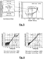
- Fig. 5 shows a second example according to the present disclosure.
- the stack schematic shows two SL laminates in this buffer structure where the total thickness is ⁇ 4 ⁇ m.
- the SL1 laminate has an equivalent Al% of 40.0% and SL2 laminate has 23.6%.
- SL1 consists of 66 repetitions; SL2 consists of 50 repetitions.
- the figure on the right is the in situ wafer curvature recorded during the growth of this stack, where the sharp spikes and short range high frequency oscillations of the curves are the artefacts of the measurement system.
- the positive curvature represents a convex wafer shape and negative curvature represents a concave wafer shape.
- the slope of the in situ wafer curvature is proportional to the in-plane stress at the growth front. A positive slope indicates a compressive in-plane stress and a negative slope indicates a tensile in-plane stress.
- the in situ wafer curvature indicates that throughout the SL growth, a compressive stress can be maintained which can effectively compensate the tensile stress during the cooling in order to minimize the epitaxial wafer warp. Especially, a clear increase of the slope of the in situ curvature can be seen when SL2 laminate starts to grow. This is due to the lattice mismatch introduced compressive stress when growing SL2 on SL1 laminate because the equivalent Al% in SL2 laminate is less than SL1 laminate (while the compressive strain of SL1 laminate is already sufficiently relaxed before growing SL2 laminate), even though the Al% in the AIGaN layer in both SL1 and SL2 laminates is the same.
- the regions indicated by the dashed boxes represent in situ curvature during growth of SL1 and SL2 laminates, respectively.
- the final epitaxial wafer warp (after cooling) is about -20 ⁇ m.
- the positive sign of the warp follows the same as for in situ curvature (i.e. convex wafer shape).
- typical SPEC for wafer warp is ⁇ ⁇ 50 ⁇ m and a positive warp is more favorable for the stability of epitaxial wafer integrity. So the final warp is within acceptable limits.
- Fig. 6 shows the vertical buffer breakdown (Vbd) measurement results at 25°C and 150°C. The measurements prove a high breakdown voltage even though the total buffer structure thickness is only 4.14 ⁇ m.
- a stack with a single SL laminate is shown in Figs. 7 and 8 .
- the SL laminate consists of 100 repetitions of the same SL unit as the SL2 laminate in examples 1 and 2, namely an AlN layer (5 nm) with an AlGaN layer on top (28 nm) with 10% Al.
- the total stack thickness is ⁇ 5.4 ⁇ m. Because it has only one SL laminate, there is no additional compressive stress introduced during SL growth, and the wafer warp at room temperature (25°C) is ⁇ -40 ⁇ m which is also less favorable.
- the Vbd of this stack is similar to that of the examples 1 and 2, its thickness is much higher. As a result, the breakdown field strength of the reference stack is in comparison much lower.
- Fig. 9 shows a summary of the Vbd measurements of the two examples and the reference under both bias polarities and at 25°C and 150°C, respectively. The figure clearly shows that the breakdown field strength is much higher for the two examples than the reference under all conditions, especially at 150°C.
- Fig. 10 is provided as an explanation for the preferred thickness of at least one superlattice laminate, which is preferably enough to allow sufficient strain relaxation of the superlattice laminate.
- the sharp spikes and short range high frequency oscillations of the curves are the artefacts of the measurement system.
- the preferred thickness corresponds to the thickness where the slope of the wafer in situ curvature appreciably decreases (the addition of SL units is continued at least until the slope of the in situ wafer curvature drops below 0.015 km-1/s). This thickness depends on the average aluminum content of as well as the layer structure of the said superlattice laminate.
- the figure gives an example: the arrow indicates where the slope of the in situ wafer curvature is considered as appreciably decreasing, so where a suitable thickness for the strain relaxation has been obtained.
- Fig. 10 merely represents one example and that the growth of the buffer layer structure may be performed such that an at least partial in-plane strain relaxation occurs between one adjacent pair of layers within a lower, middle or top portion of the first or the second superlattice laminate.
- Said pair may include a lower layer and an upper layer formed on the lower layer wherein the upper layer, during the growth of the buffer layer structure, becomes or is formed to be at least partially strain relaxed with respect to the lower layer.
- the strain relaxation may be achieved for instance by growing the upper layer to a thickness exceeding a critical layer thickness.
- the upper layer may be grown as a pseudomorphic layer (i.e. thinner than the critical thickness) and subsequently, following growth of further layers on top, become partially strain relaxed.
- Strain relaxation may occur at one or more positions within the first superlattice laminate and/or within the second superlattice laminate. All other layers of the superlattice laminate(s) may form pseudomorphic layers. For instance, in the example of Fig. 5 it may be seen that that strain relaxation occurs already in a lower portion of the SL1.
- an at least partial strain relaxation may be present in the buffer layer structure, between (at least) said lower and adjacent upper layer.
- the in-plane lattice constant of the upper layer matches the in-plane lattice constant of the lower layer.
Landscapes
- Junction Field-Effect Transistors (AREA)
- Recrystallisation Techniques (AREA)
Claims (11)
- III-N-basiertes Substrat für leistungselektronische Vorrichtungen, umfassend ein Basissubstrat, ein III-N-Laminat über dem Basissubstrat und eine Pufferschichtstruktur zwischen dem Basissubstrat und dem III-N-Laminat, wobei
die Pufferschichtstruktur mindestens ein erstes Übergitterlaminat und ein zweites Übergitterlaminat über dem ersten Übergitterlaminat umfasst;
das erste Übergitterlaminat eine Wiederholung einer ersten Übergittereinheit umfasst, die aus einer Vielzahl von ersten AlGaN-Schichten besteht, die jeweils aus AlxGa1-xN bestehen, wobei 0≤x≤1 und x für die ersten AlGaN-Schichten unterschiedlich ist;
das zweite Übergitterlaminat eine Wiederholung einer zweiten Übergittereinheit umfasst, die aus einer Vielzahl von zweiten AlGaN-Schichten besteht, die jeweils aus AlyGa1-yN bestehen, wobei 0≤y≤1 und y für die zweiten AlGaN-Schichten unterschiedlich ist; und
ein durchschnittlicher Aluminiumgehalt des ersten Übergitterlaminats um eine vorbestimmte Differenz größer als ein durchschnittlicher Aluminiumgehalt des zweiten Übergitterlaminats ist,
dadurch gekennzeichnet, dass:eine mindestens teilweise Verformungsrelaxation in der Pufferschichtstruktur zwischen mindestens einem angrenzenden Paar von Schichten des ersten und/oder des zweiten Übergitterlaminats vorliegt; undder durchschnittliche Aluminiumgehalt des ersten Übergitterlaminats mindestens 30 % beträgt und die vorbestimmte Differenz mindestens 5 % ist. - III-N-basiertes Substrat nach Anspruch 1, wobei infolge der vorbestimmten Differenz des Aluminiumgehalts die Pufferschichtstruktur eine Durchbruchfeldstärke von mehr als 150 V/µm bei senkrechter Durchlass- und/oder Sperrspannung bei einer Raumtemperatur von 25 °C aufweist.
- III-N-basiertes Substrat nach Anspruch 1 oder 2, wobei die vorbestimmte Differenz die Substratverwerfung bei einer Raumtemperatur von 25 °C steuert, damit sie für ein Substrat mit einem Durchmesser von 200 mm unter 50 µm liegt.
- III-N-basiertes Substrat nach einem der vorhergehenden Ansprüche, wobei die Pufferschichtstruktur mindestens ein zusätzliches Übergitterlaminat auf dem zweiten Übergitterlaminat umfasst, wobei
jedes zusätzliche Übergitterlaminat eine Wiederholung einer jeweiligen dritten Übergittereinheit umfasst, die aus einer Vielzahl von jeweiligen dritten AlGaN-Schichten besteht, die jeweils aus AliGa1-iN bestehen, wobei 0≤i≤1 und i für die jeweiligen dritten AlGaN-Schichten der jeweiligen dritten Übergittereinheit unterschiedlich ist; und
der durchschnittliche Aluminiumgehalt des ersten Übergitterlaminats um mindestens 5 % größer als der durchschnittliche Aluminiumgehalt des zweiten Übergitterlaminats ist, und der durchschnittliche Aluminiumgehalt des zweiten Übergitterlaminats um mindestens 5 % größer als der durchschnittliche Aluminiumgehalt des zusätzlichen Übergitterlaminats ist. - III-N-basiertes Substrat nach Anspruch 4, wobei der durchschnittliche Aluminiumgehalt des zusätzlichen Übergitterlaminats mindestens 5 % beträgt.
- III-N-basiertes Substrat nach einem der vorhergehenden Ansprüche, wobei die erste, zweite und/oder zusätzliche Übergittereinheit aus mindestens drei AIGaN-Schichten bestehen.
- III-N-basiertes Substrat nach Anspruch 6, wobei die erste, zweite und/oder dritte Übergittereinheit eine Schicht aus AljGa1-jN umfassen, wobei 0≤j≤0,5.
- III-N-basiertes Substrat nach einem der vorhergehenden Ansprüche, wobei eine oder mehrere Schichten, die aus dem ersten, zweiten und/oder dritten Übergitterlaminat ausgewählt werden, Fremdatome enthalten, wobei die Fremdatome eine oder mehrere Arten, die aus der Gruppe, die aus C-Atomen, Fe-Atomen, Mn-Atomen, Mg-Atomen, V-Atomen, Cr-Atomen, Be-Atomen und B-Atomen, besteht, ausgewählt werden, bevorzugt C-Atomen oder Fe-Atomen, sind.
- Verfahren zum Herstellen eines III-N-basierten Substrats für leistungselektronische Vorrichtungen, umfassend folgende Schritte: Bereitstellen eines Basissubstrats, Ziehen einer Pufferschichtstruktur auf dem Basissubstrat und Ziehen eines III-N-Laminats auf der Pufferschichtstruktur, wobei:die Pufferschichtstruktur mindestens ein erstes Übergitterlaminat und ein zweites Übergitterlaminat über dem ersten Übergitterlaminat umfasst;das erste Übergitterlaminat eine Wiederholung einer ersten Übergittereinheit umfasst, die aus einer Vielzahl von ersten AlGaN-Schichten besteht, die jeweils aus AlxGa1-xN bestehen, wobei 0≤x≤1 und x für die ersten AlGaN-Schichten unterschiedlich ist;das zweite Übergitterlaminat eine Wiederholung einer zweiten Übergittereinheit umfasst, die aus einer Vielzahl von zweiten AlGaN-Schichten besteht, die jeweils aus AlyGa1-yN bestehen, wobei 0≤y≤1 und y für zweiten AlGaN-Schichten unterschiedlich ist; undnach dem Ziehen der Pufferschichtstruktur die Prozessbedingungen derart gesteuert werden, dass ein durchschnittlicher Aluminiumgehalt des ersten Übergitterlaminats um eine vorbestimmte Differenz größer als ein durchschnittlicher Aluminiumgehalt des zweiten Übergitterlaminats ist;dadurch gekennzeichnet, dass der durchschnittliche Aluminiumgehalt des ersten Übergitterlaminats mindestens 30 % beträgt und die vorbestimmte Differenz mindestens 5 % ist; und dass für mindestens ein Übergitterlaminat das Wachstum von Übergittereinheiten mindestens fortfährt, bis die Steigung der In-situ-Wafer-Krümmung unter 0,015 km-1/s abfällt.
- Verfahren nach Anspruch 9, wobei die erste und zweite Übergittereinheit die gleiche Schichtstruktur aufweisen, bis auf eine Variation des Aluminiumgehalts und/oder der Dicke mindestens einer der AlGaN-Schichten, um den durchschnittlichen Aluminiumgehalt der Übergittereinheiten und somit des Übergitterlaminats zu beeinflussen.
- Verfahren nach einem der Ansprüche 9 bis 10, wobei die Pufferschichtstruktur derart gezogen wird, dass eine mindestens teilweise Verformungsrelaxation zwischen mindestens einem angrenzenden Paar von Schichten des ersten und/oder des zweiten Übergitterlaminats vorkommt.
Applications Claiming Priority (1)
| Application Number | Priority Date | Filing Date | Title |
|---|---|---|---|
| EP17152589 | 2017-01-23 |
Publications (2)
| Publication Number | Publication Date |
|---|---|
| EP3352199A1 EP3352199A1 (de) | 2018-07-25 |
| EP3352199B1 true EP3352199B1 (de) | 2021-07-14 |
Family
ID=57906453
Family Applications (1)
| Application Number | Title | Priority Date | Filing Date |
|---|---|---|---|
| EP17202493.7A Active EP3352199B1 (de) | 2017-01-23 | 2017-11-20 | Iii-n-basiertes substrat für leistungselektronische vorrichtungen und verfahren zur herstellung davon |
Country Status (5)
| Country | Link |
|---|---|
| US (1) | US10192959B2 (de) |
| EP (1) | EP3352199B1 (de) |
| JP (1) | JP7158842B2 (de) |
| CN (1) | CN108346694B (de) |
| TW (1) | TWI670852B (de) |
Families Citing this family (10)
| Publication number | Priority date | Publication date | Assignee | Title |
|---|---|---|---|---|
| US10720520B2 (en) | 2017-06-21 | 2020-07-21 | Infineon Technologies Austria Ag | Method of controlling wafer bow in a type III-V semiconductor device |
| EP3576132B1 (de) * | 2018-05-28 | 2025-12-17 | IMEC vzw | Iii-n-halbleiterstruktur und verfahren zur formung einer iii-n-halbleiterstruktur |
| US11552217B2 (en) * | 2018-11-12 | 2023-01-10 | Epistar Corporation | Semiconductor device |
| US10562130B1 (en) | 2018-12-29 | 2020-02-18 | Cree, Inc. | Laser-assisted method for parting crystalline material |
| US10611052B1 (en) | 2019-05-17 | 2020-04-07 | Cree, Inc. | Silicon carbide wafers with relaxed positive bow and related methods |
| CN112368841B (zh) | 2020-06-23 | 2023-03-14 | 英诺赛科(珠海)科技有限公司 | 半导体装置结构和其制造方法 |
| CN115548087B (zh) * | 2021-06-29 | 2026-02-03 | 世界先进积体电路股份有限公司 | 半导体结构及高电子迁移率晶体管 |
| JP7378562B2 (ja) * | 2021-10-27 | 2023-11-13 | 財團法人工業技術研究院 | 平衡応力を有する半導体基板 |
| US12520548B2 (en) | 2021-10-27 | 2026-01-06 | Industrial Technology Research Institute | Semiconductor substrate with balanced stress |
| CN119403191A (zh) * | 2024-12-30 | 2025-02-07 | 中微半导体(上海)有限公司 | 用于GaN HEMT的超晶格结构、缓冲层、GaN HEMT外延片及生长方法 |
Family Cites Families (24)
| Publication number | Priority date | Publication date | Assignee | Title |
|---|---|---|---|---|
| JP3778765B2 (ja) | 2000-03-24 | 2006-05-24 | 三洋電機株式会社 | 窒化物系半導体素子およびその製造方法 |
| JP2003077835A (ja) * | 2001-09-06 | 2003-03-14 | Ngk Insulators Ltd | Iii族窒化物素子及びiii族窒化物エピタキシャル基板 |
| WO2005106985A2 (en) * | 2004-04-22 | 2005-11-10 | Cree, Inc. | Improved substrate buffer structure for group iii nitride devices |
| EP1933384B1 (de) * | 2006-12-15 | 2013-02-13 | Soitec | Halbleiter-Heterostruktur |
| JP5309452B2 (ja) | 2007-02-28 | 2013-10-09 | サンケン電気株式会社 | 半導体ウエーハ及び半導体素子及び製造方法 |
| KR20120022872A (ko) * | 2009-05-22 | 2012-03-12 | 스미또모 가가꾸 가부시키가이샤 | 반도체 기판, 전자 디바이스, 반도체 기판의 제조 방법 및 전자 디바이스의 제조 방법 |
| EP2498282A4 (de) | 2009-11-04 | 2014-06-25 | Dowa Electronics Materials Co Ltd | Epitaktisch beschichtetes gruppe-iii-nitrid-substrat |
| US8816395B2 (en) * | 2010-05-02 | 2014-08-26 | Visic Technologies Ltd. | Field effect power transistors |
| JP5706102B2 (ja) * | 2010-05-07 | 2015-04-22 | ローム株式会社 | 窒化物半導体素子 |
| US20120126239A1 (en) * | 2010-11-24 | 2012-05-24 | Transphorm Inc. | Layer structures for controlling stress of heteroepitaxially grown iii-nitride layers |
| CN102162137B (zh) * | 2011-01-28 | 2013-05-29 | 中国科学院上海硅酸盐研究所 | 一种高质量应变的Ge/SiGe超晶格结构及其制备方法 |
| JP5665676B2 (ja) * | 2011-07-11 | 2015-02-04 | Dowaエレクトロニクス株式会社 | Iii族窒化物エピタキシャル基板およびその製造方法 |
| JP5514920B2 (ja) * | 2012-01-13 | 2014-06-04 | Dowaエレクトロニクス株式会社 | Iii族窒化物エピタキシャル基板および該基板を用いた深紫外発光素子 |
| US8742396B2 (en) | 2012-01-13 | 2014-06-03 | Dowa Electronics Materials Co., Ltd. | III nitride epitaxial substrate and deep ultraviolet light emitting device using the same |
| JP5785103B2 (ja) | 2012-01-16 | 2015-09-24 | シャープ株式会社 | ヘテロ接合型電界効果トランジスタ用のエピタキシャルウエハ |
| KR20130139707A (ko) | 2012-06-13 | 2013-12-23 | 삼성전자주식회사 | 반도체 소자 및 이에 사용되는 초격자층 |
| KR20130141290A (ko) | 2012-06-15 | 2013-12-26 | 삼성전자주식회사 | 초격자 구조체 및 이를 포함한 반도체 소자 |
| CN103578926B (zh) * | 2012-08-09 | 2018-01-02 | 三星电子株式会社 | 半导体缓冲结构、半导体器件和制造半导体器件的方法 |
| JP5841085B2 (ja) * | 2013-02-26 | 2016-01-06 | 日本電信電話株式会社 | 半導体緩衝層の構造決定方法 |
| EP2779213B1 (de) * | 2013-03-12 | 2015-05-06 | Siltronic AG | Halbleiter-Wafer mit einer Schicht aus AlzGa1-zN und Herstellungsverfahren |
| DE112014003533T5 (de) * | 2013-07-30 | 2016-04-14 | Sumitomo Chemical Company, Limited | Halbleiterwafer und Verfahren zur Herstellung des Halbleiterwafers |
| JP2015053328A (ja) | 2013-09-05 | 2015-03-19 | 富士通株式会社 | 半導体装置 |
| GB2519338A (en) * | 2013-10-17 | 2015-04-22 | Nanogan Ltd | Crack-free gallium nitride materials |
| US20160359004A1 (en) * | 2015-06-03 | 2016-12-08 | Veeco Instruments, Inc. | Stress control for heteroepitaxy |
-
2017
- 2017-11-20 EP EP17202493.7A patent/EP3352199B1/de active Active
- 2017-11-20 JP JP2017222407A patent/JP7158842B2/ja active Active
- 2017-11-20 TW TW106140099A patent/TWI670852B/zh active
- 2017-11-20 CN CN201711160172.5A patent/CN108346694B/zh active Active
- 2017-11-20 US US15/817,343 patent/US10192959B2/en active Active
Also Published As
| Publication number | Publication date |
|---|---|
| JP7158842B2 (ja) | 2022-10-24 |
| US20180212025A1 (en) | 2018-07-26 |
| JP2018174296A (ja) | 2018-11-08 |
| TW201828468A (zh) | 2018-08-01 |
| CN108346694A (zh) | 2018-07-31 |
| CN108346694B (zh) | 2020-10-02 |
| TWI670852B (zh) | 2019-09-01 |
| US10192959B2 (en) | 2019-01-29 |
| EP3352199A1 (de) | 2018-07-25 |
Similar Documents
| Publication | Publication Date | Title |
|---|---|---|
| US10192959B2 (en) | III-N based substrate for power electronic devices and method for manufacturing same | |
| KR101527638B1 (ko) | 전자 디바이스용 에피택셜 기판 및 그 제조 방법 | |
| JP5309452B2 (ja) | 半導体ウエーハ及び半導体素子及び製造方法 | |
| JP6638033B2 (ja) | 半導体基板および半導体基板の製造方法 | |
| JP4592742B2 (ja) | 半導体材料、半導体材料の製造方法及び半導体素子 | |
| EP2469583B1 (de) | Stress-modulierte Gruppe III-V-Halbleitervorrichtung und zugehöriges Verfahren | |
| US7271416B2 (en) | Strain compensated semiconductor structures | |
| US8530935B2 (en) | Semiconductor device with buffer layer for mitigating stress exerted on compound semiconductor layer | |
| JP5836158B2 (ja) | 歪吸収中間層遷移モジュールを有するiii族窒化物半導体構造 | |
| KR101186032B1 (ko) | 질화갈륨 또는 질화알루미늄갈륨 층을 제조하는 방법 | |
| US10818491B2 (en) | Formation of a III-N semiconductor structure | |
| JP2011082494A (ja) | 化合物半導体基板 | |
| CA2468520A1 (en) | Strain balanced nitride heterojunction transistors and methods of fabricating strain balanced nitride heterojunction transistors | |
| US8633569B1 (en) | AlN inter-layers in III-N material grown on REO/silicon substrate | |
| US20170229549A1 (en) | Semiconductor structure comprising an active semiconductor layer of the iii-v type on a buffer layer stack and method for producing semiconductor structure | |
| JP2009289956A (ja) | 半導体電子デバイス | |
| CN103314429A (zh) | 用于控制异质外延生长的iii族氮化物层的应力的层结构 | |
| US20170323960A1 (en) | Epitaxial wafer, semiconductor device, method for producing epitaxial wafer, and method for producing semiconductor device | |
| US20150263099A1 (en) | Semiconductor device | |
| US20190051515A1 (en) | Semiconductor base and semiconductor device | |
| US20140231817A1 (en) | Iii-n material grown on alo/aln buffer on si substrate | |
| US9401420B2 (en) | Semiconductor device | |
| JP7034739B2 (ja) | 窒化物半導体基板およびその製造方法 | |
| TWI441331B (zh) | A epitaxial substrate for electronic components and a method for manufacturing the same | |
| CN106783955B (zh) | 含有氮镓铝和氮镓铟的插入层的半导体器件及其制造方法 |
Legal Events
| Date | Code | Title | Description |
|---|---|---|---|
| PUAI | Public reference made under article 153(3) epc to a published international application that has entered the european phase |
Free format text: ORIGINAL CODE: 0009012 |
|
| STAA | Information on the status of an ep patent application or granted ep patent |
Free format text: STATUS: THE APPLICATION HAS BEEN PUBLISHED |
|
| AK | Designated contracting states |
Kind code of ref document: A1 Designated state(s): AL AT BE BG CH CY CZ DE DK EE ES FI FR GB GR HR HU IE IS IT LI LT LU LV MC MK MT NL NO PL PT RO RS SE SI SK SM TR |
|
| AX | Request for extension of the european patent |
Extension state: BA ME |
|
| STAA | Information on the status of an ep patent application or granted ep patent |
Free format text: STATUS: REQUEST FOR EXAMINATION WAS MADE |
|
| 17P | Request for examination filed |
Effective date: 20190125 |
|
| RBV | Designated contracting states (corrected) |
Designated state(s): AL AT BE BG CH CY CZ DE DK EE ES FI FR GB GR HR HU IE IS IT LI LT LU LV MC MK MT NL NO PL PT RO RS SE SI SK SM TR |
|
| GRAP | Despatch of communication of intention to grant a patent |
Free format text: ORIGINAL CODE: EPIDOSNIGR1 |
|
| STAA | Information on the status of an ep patent application or granted ep patent |
Free format text: STATUS: GRANT OF PATENT IS INTENDED |
|
| INTG | Intention to grant announced |
Effective date: 20210222 |
|
| GRAS | Grant fee paid |
Free format text: ORIGINAL CODE: EPIDOSNIGR3 |
|
| GRAA | (expected) grant |
Free format text: ORIGINAL CODE: 0009210 |
|
| STAA | Information on the status of an ep patent application or granted ep patent |
Free format text: STATUS: THE PATENT HAS BEEN GRANTED |
|
| AK | Designated contracting states |
Kind code of ref document: B1 Designated state(s): AL AT BE BG CH CY CZ DE DK EE ES FI FR GB GR HR HU IE IS IT LI LT LU LV MC MK MT NL NO PL PT RO RS SE SI SK SM TR |
|
| REG | Reference to a national code |
Ref country code: GB Ref legal event code: FG4D |
|
| REG | Reference to a national code |
Ref country code: IE Ref legal event code: FG4D |
|
| REG | Reference to a national code |
Ref country code: DE Ref legal event code: R096 Ref document number: 602017042035 Country of ref document: DE |
|
| REG | Reference to a national code |
Ref country code: AT Ref legal event code: REF Ref document number: 1411308 Country of ref document: AT Kind code of ref document: T Effective date: 20210815 |
|
| REG | Reference to a national code |
Ref country code: LT Ref legal event code: MG9D |
|
| REG | Reference to a national code |
Ref country code: NL Ref legal event code: MP Effective date: 20210714 |
|
| REG | Reference to a national code |
Ref country code: AT Ref legal event code: MK05 Ref document number: 1411308 Country of ref document: AT Kind code of ref document: T Effective date: 20210714 |
|
| PG25 | Lapsed in a contracting state [announced via postgrant information from national office to epo] |
Ref country code: SE Free format text: LAPSE BECAUSE OF FAILURE TO SUBMIT A TRANSLATION OF THE DESCRIPTION OR TO PAY THE FEE WITHIN THE PRESCRIBED TIME-LIMIT Effective date: 20210714 Ref country code: RS Free format text: LAPSE BECAUSE OF FAILURE TO SUBMIT A TRANSLATION OF THE DESCRIPTION OR TO PAY THE FEE WITHIN THE PRESCRIBED TIME-LIMIT Effective date: 20210714 Ref country code: HR Free format text: LAPSE BECAUSE OF FAILURE TO SUBMIT A TRANSLATION OF THE DESCRIPTION OR TO PAY THE FEE WITHIN THE PRESCRIBED TIME-LIMIT Effective date: 20210714 Ref country code: AT Free format text: LAPSE BECAUSE OF FAILURE TO SUBMIT A TRANSLATION OF THE DESCRIPTION OR TO PAY THE FEE WITHIN THE PRESCRIBED TIME-LIMIT Effective date: 20210714 Ref country code: BG Free format text: LAPSE BECAUSE OF FAILURE TO SUBMIT A TRANSLATION OF THE DESCRIPTION OR TO PAY THE FEE WITHIN THE PRESCRIBED TIME-LIMIT Effective date: 20211014 Ref country code: LT Free format text: LAPSE BECAUSE OF FAILURE TO SUBMIT A TRANSLATION OF THE DESCRIPTION OR TO PAY THE FEE WITHIN THE PRESCRIBED TIME-LIMIT Effective date: 20210714 Ref country code: NL Free format text: LAPSE BECAUSE OF FAILURE TO SUBMIT A TRANSLATION OF THE DESCRIPTION OR TO PAY THE FEE WITHIN THE PRESCRIBED TIME-LIMIT Effective date: 20210714 Ref country code: PT Free format text: LAPSE BECAUSE OF FAILURE TO SUBMIT A TRANSLATION OF THE DESCRIPTION OR TO PAY THE FEE WITHIN THE PRESCRIBED TIME-LIMIT Effective date: 20211115 Ref country code: NO Free format text: LAPSE BECAUSE OF FAILURE TO SUBMIT A TRANSLATION OF THE DESCRIPTION OR TO PAY THE FEE WITHIN THE PRESCRIBED TIME-LIMIT Effective date: 20211014 Ref country code: FI Free format text: LAPSE BECAUSE OF FAILURE TO SUBMIT A TRANSLATION OF THE DESCRIPTION OR TO PAY THE FEE WITHIN THE PRESCRIBED TIME-LIMIT Effective date: 20210714 Ref country code: ES Free format text: LAPSE BECAUSE OF FAILURE TO SUBMIT A TRANSLATION OF THE DESCRIPTION OR TO PAY THE FEE WITHIN THE PRESCRIBED TIME-LIMIT Effective date: 20210714 |
|
| PG25 | Lapsed in a contracting state [announced via postgrant information from national office to epo] |
Ref country code: PL Free format text: LAPSE BECAUSE OF FAILURE TO SUBMIT A TRANSLATION OF THE DESCRIPTION OR TO PAY THE FEE WITHIN THE PRESCRIBED TIME-LIMIT Effective date: 20210714 Ref country code: LV Free format text: LAPSE BECAUSE OF FAILURE TO SUBMIT A TRANSLATION OF THE DESCRIPTION OR TO PAY THE FEE WITHIN THE PRESCRIBED TIME-LIMIT Effective date: 20210714 Ref country code: GR Free format text: LAPSE BECAUSE OF FAILURE TO SUBMIT A TRANSLATION OF THE DESCRIPTION OR TO PAY THE FEE WITHIN THE PRESCRIBED TIME-LIMIT Effective date: 20211015 |
|
| REG | Reference to a national code |
Ref country code: DE Ref legal event code: R097 Ref document number: 602017042035 Country of ref document: DE |
|
| PG25 | Lapsed in a contracting state [announced via postgrant information from national office to epo] |
Ref country code: DK Free format text: LAPSE BECAUSE OF FAILURE TO SUBMIT A TRANSLATION OF THE DESCRIPTION OR TO PAY THE FEE WITHIN THE PRESCRIBED TIME-LIMIT Effective date: 20210714 |
|
| PLBE | No opposition filed within time limit |
Free format text: ORIGINAL CODE: 0009261 |
|
| STAA | Information on the status of an ep patent application or granted ep patent |
Free format text: STATUS: NO OPPOSITION FILED WITHIN TIME LIMIT |
|
| PG25 | Lapsed in a contracting state [announced via postgrant information from national office to epo] |
Ref country code: SM Free format text: LAPSE BECAUSE OF FAILURE TO SUBMIT A TRANSLATION OF THE DESCRIPTION OR TO PAY THE FEE WITHIN THE PRESCRIBED TIME-LIMIT Effective date: 20210714 Ref country code: SK Free format text: LAPSE BECAUSE OF FAILURE TO SUBMIT A TRANSLATION OF THE DESCRIPTION OR TO PAY THE FEE WITHIN THE PRESCRIBED TIME-LIMIT Effective date: 20210714 Ref country code: RO Free format text: LAPSE BECAUSE OF FAILURE TO SUBMIT A TRANSLATION OF THE DESCRIPTION OR TO PAY THE FEE WITHIN THE PRESCRIBED TIME-LIMIT Effective date: 20210714 Ref country code: EE Free format text: LAPSE BECAUSE OF FAILURE TO SUBMIT A TRANSLATION OF THE DESCRIPTION OR TO PAY THE FEE WITHIN THE PRESCRIBED TIME-LIMIT Effective date: 20210714 Ref country code: CZ Free format text: LAPSE BECAUSE OF FAILURE TO SUBMIT A TRANSLATION OF THE DESCRIPTION OR TO PAY THE FEE WITHIN THE PRESCRIBED TIME-LIMIT Effective date: 20210714 Ref country code: AL Free format text: LAPSE BECAUSE OF FAILURE TO SUBMIT A TRANSLATION OF THE DESCRIPTION OR TO PAY THE FEE WITHIN THE PRESCRIBED TIME-LIMIT Effective date: 20210714 |
|
| 26N | No opposition filed |
Effective date: 20220419 |
|
| PG25 | Lapsed in a contracting state [announced via postgrant information from national office to epo] |
Ref country code: MC Free format text: LAPSE BECAUSE OF FAILURE TO SUBMIT A TRANSLATION OF THE DESCRIPTION OR TO PAY THE FEE WITHIN THE PRESCRIBED TIME-LIMIT Effective date: 20210714 |
|
| REG | Reference to a national code |
Ref country code: CH Ref legal event code: PL |
|
| GBPC | Gb: european patent ceased through non-payment of renewal fee |
Effective date: 20211120 |
|
| PG25 | Lapsed in a contracting state [announced via postgrant information from national office to epo] |
Ref country code: LU Free format text: LAPSE BECAUSE OF NON-PAYMENT OF DUE FEES Effective date: 20211120 Ref country code: IT Free format text: LAPSE BECAUSE OF FAILURE TO SUBMIT A TRANSLATION OF THE DESCRIPTION OR TO PAY THE FEE WITHIN THE PRESCRIBED TIME-LIMIT Effective date: 20210714 Ref country code: BE Free format text: LAPSE BECAUSE OF NON-PAYMENT OF DUE FEES Effective date: 20211130 |
|
| REG | Reference to a national code |
Ref country code: BE Ref legal event code: MM Effective date: 20211130 |
|
| PG25 | Lapsed in a contracting state [announced via postgrant information from national office to epo] |
Ref country code: LI Free format text: LAPSE BECAUSE OF NON-PAYMENT OF DUE FEES Effective date: 20211130 Ref country code: CH Free format text: LAPSE BECAUSE OF NON-PAYMENT OF DUE FEES Effective date: 20211130 |
|
| PG25 | Lapsed in a contracting state [announced via postgrant information from national office to epo] |
Ref country code: IE Free format text: LAPSE BECAUSE OF NON-PAYMENT OF DUE FEES Effective date: 20211120 Ref country code: GB Free format text: LAPSE BECAUSE OF NON-PAYMENT OF DUE FEES Effective date: 20211120 |
|
| PG25 | Lapsed in a contracting state [announced via postgrant information from national office to epo] |
Ref country code: FR Free format text: LAPSE BECAUSE OF NON-PAYMENT OF DUE FEES Effective date: 20211130 |
|
| PG25 | Lapsed in a contracting state [announced via postgrant information from national office to epo] |
Ref country code: HU Free format text: LAPSE BECAUSE OF FAILURE TO SUBMIT A TRANSLATION OF THE DESCRIPTION OR TO PAY THE FEE WITHIN THE PRESCRIBED TIME-LIMIT; INVALID AB INITIO Effective date: 20171120 |
|
| P01 | Opt-out of the competence of the unified patent court (upc) registered |
Effective date: 20230513 |
|
| PG25 | Lapsed in a contracting state [announced via postgrant information from national office to epo] |
Ref country code: CY Free format text: LAPSE BECAUSE OF FAILURE TO SUBMIT A TRANSLATION OF THE DESCRIPTION OR TO PAY THE FEE WITHIN THE PRESCRIBED TIME-LIMIT Effective date: 20210714 |
|
| PG25 | Lapsed in a contracting state [announced via postgrant information from national office to epo] |
Ref country code: MK Free format text: LAPSE BECAUSE OF FAILURE TO SUBMIT A TRANSLATION OF THE DESCRIPTION OR TO PAY THE FEE WITHIN THE PRESCRIBED TIME-LIMIT Effective date: 20210714 |
|
| PG25 | Lapsed in a contracting state [announced via postgrant information from national office to epo] |
Ref country code: MT Free format text: LAPSE BECAUSE OF FAILURE TO SUBMIT A TRANSLATION OF THE DESCRIPTION OR TO PAY THE FEE WITHIN THE PRESCRIBED TIME-LIMIT Effective date: 20210714 |
|
| REG | Reference to a national code |
Ref country code: DE Ref legal event code: R079 Ref document number: 602017042035 Country of ref document: DE Free format text: PREVIOUS MAIN CLASS: H01L0021200000 Ipc: H10P0014200000 |
|
| PG25 | Lapsed in a contracting state [announced via postgrant information from national office to epo] |
Ref country code: TR Free format text: LAPSE BECAUSE OF FAILURE TO SUBMIT A TRANSLATION OF THE DESCRIPTION OR TO PAY THE FEE WITHIN THE PRESCRIBED TIME-LIMIT Effective date: 20210714 |
|
| PGFP | Annual fee paid to national office [announced via postgrant information from national office to epo] |
Ref country code: DE Payment date: 20251022 Year of fee payment: 9 |