EP3320619B1 - Spannungsverstärker für einen programmierbaren spannungsbereich - Google Patents
Spannungsverstärker für einen programmierbaren spannungsbereich Download PDFInfo
- Publication number
- EP3320619B1 EP3320619B1 EP16742190.8A EP16742190A EP3320619B1 EP 3320619 B1 EP3320619 B1 EP 3320619B1 EP 16742190 A EP16742190 A EP 16742190A EP 3320619 B1 EP3320619 B1 EP 3320619B1
- Authority
- EP
- European Patent Office
- Prior art keywords
- signal
- amplifier
- voltage
- input
- input voltage
- Prior art date
- Legal status (The legal status is an assumption and is not a legal conclusion. Google has not performed a legal analysis and makes no representation as to the accuracy of the status listed.)
- Active
Links
Images


Classifications
-
- H—ELECTRICITY
- H03—ELECTRONIC CIRCUITRY
- H03M—CODING; DECODING; CODE CONVERSION IN GENERAL
- H03M1/00—Analogue/digital conversion; Digital/analogue conversion
- H03M1/12—Analogue/digital converters
- H03M1/18—Automatic control for modifying the range of signals the converter can handle, e.g. gain ranging
- H03M1/188—Multi-path, i.e. having a separate analogue/digital converter for each possible range
-
- H—ELECTRICITY
- H03—ELECTRONIC CIRCUITRY
- H03F—AMPLIFIERS
- H03F3/00—Amplifiers with only discharge tubes or only semiconductor devices as amplifying elements
- H03F3/45—Differential amplifiers
- H03F3/45071—Differential amplifiers with semiconductor devices only
- H03F3/45076—Differential amplifiers with semiconductor devices only characterised by the way of implementation of the active amplifying circuit in the differential amplifier
- H03F3/45179—Differential amplifiers with semiconductor devices only characterised by the way of implementation of the active amplifying circuit in the differential amplifier using MOSFET transistors as the active amplifying circuit
- H03F3/45183—Long tailed pairs
-
- H—ELECTRICITY
- H03—ELECTRONIC CIRCUITRY
- H03F—AMPLIFIERS
- H03F3/00—Amplifiers with only discharge tubes or only semiconductor devices as amplifying elements
- H03F3/45—Differential amplifiers
- H03F3/45071—Differential amplifiers with semiconductor devices only
- H03F3/45076—Differential amplifiers with semiconductor devices only characterised by the way of implementation of the active amplifying circuit in the differential amplifier
- H03F3/45475—Differential amplifiers with semiconductor devices only characterised by the way of implementation of the active amplifying circuit in the differential amplifier using IC blocks as the active amplifying circuit
-
- H—ELECTRICITY
- H03—ELECTRONIC CIRCUITRY
- H03M—CODING; DECODING; CODE CONVERSION IN GENERAL
- H03M1/00—Analogue/digital conversion; Digital/analogue conversion
- H03M1/12—Analogue/digital converters
- H03M1/124—Sampling or signal conditioning arrangements specially adapted for A/D converters
- H03M1/129—Means for adapting the input signal to the range the converter can handle, e.g. limiting, pre-scaling ; Out-of-range indication
- H03M1/1295—Clamping, i.e. adjusting the DC level of the input signal to a predetermined value
-
- H—ELECTRICITY
- H03—ELECTRONIC CIRCUITRY
- H03F—AMPLIFIERS
- H03F2203/00—Indexing scheme relating to amplifiers with only discharge tubes or only semiconductor devices as amplifying elements covered by H03F3/00
- H03F2203/45—Indexing scheme relating to differential amplifiers
- H03F2203/45674—Indexing scheme relating to differential amplifiers the LC comprising one current mirror
-
- H—ELECTRICITY
- H03—ELECTRONIC CIRCUITRY
- H03F—AMPLIFIERS
- H03F2203/00—Indexing scheme relating to amplifiers with only discharge tubes or only semiconductor devices as amplifying elements covered by H03F3/00
- H03F2203/45—Indexing scheme relating to differential amplifiers
- H03F2203/45696—Indexing scheme relating to differential amplifiers the LC comprising more than two resistors
Definitions
- the invention relates to a voltage amplifier for a programmable voltage range and associated method for voltage amplification for a programmable voltage range.
- the maximum supply voltage limits the gain of the input signal.
- the input signal can only be amplified to the extent that it can still be amplified linearly.
- ADC pipeline analog-to-digital converters
- the signal is then evaluated by one or more comparators and this value subtracted from the input signal of the comparators, to then only amplify the difference, the so-called residual error.
- Pipeline ADCs need to be calibrated to avoid uncontrolled changes in the residual error due to a shift in the operating point. Pipeline ADCs can thus not be switched on and off at short notice, since this can lead to a shift in the operating points.
- the US 2014/0232577 A1 discloses an analog-to-digital converter having a first and second analog-to-digital conversion cells and a controller.
- the controller is configured to generate a control signal that generates first and second input ranges with respect to the same voltage range and first and second timers at different phases when specifying a mode of the signal indicating a first mode.
- the controller is further configured to generate a further control signal including the first and second input regions with respect to a continuous voltage range and first and second timers at the same phase when a mode specifying signal indicates a second mode.
- the WO 2004/051858 A2 discloses a method, apparatus and system for converting an input voltage to a digital output signal. Based on a comparison with a reference voltage in one or more (flash-type) analog-to-digital converters, it is used to generate the digital output signal representing the input voltage.
- the analog-to-digital converters are linear when multiple analog-to-digital converters are used.
- a voltage amplifier for a programmable voltage range has at least a first and a second operating point with respect to an input voltage signal.
- the voltage amplifier is configured to linearly transform a first range of the input voltage signal by means of the first operating point to a first output signal.
- the voltage amplifier is further configured to transform a second range of the input voltage signal by means of the second operating point linearly to a second output signal.
- the operating points of the voltage amplifier are always to be seen in this context in relation to the input voltage signal.
- different portions of the input voltage signal are shifted so that an amplifier that can linearly amplify input voltages between -5V and + 5V can also linearly amplify those portions of the input voltage signal that are outside of this voltage range.
- These areas are defined in the Area shifted, which can be strengthened linearly.
- the voltage amplifier could for this purpose, for example, have an adjustable operating point, so that in addition to the first and the second operating point, further operating points with respect to the input voltage signal can be set.
- the input voltage signal could, for example, be shifted continuously or discretely by means of adjustable resistances or reference potentials. Different ranges of periodic signals could thus be successively linearly amplified.
- the voltage amplifier could be configured in an alternative embodiment to provide the first operating point and the second operating point at the same time.
- a highly fluctuating signal that fluctuates, for example, between -10 V and +10 V with, for example, two amplifiers, the amplifiers linear only at an input voltage between -5V and + 5V strengthen.
- a first range of this input voltage signal which lies between -10 V and 0 V, is thereby shifted into the region of the one amplifier in which it amplifies linearly.
- a second range of this input voltage signal which is between 0V and 10V and is thereby shifted in the range of the other amplifier in which this linearly amplified.
- the first operating point and the second operating point are preferably set such that the first range of the input voltage signal and the second range of the input voltage signal have at least one common value. It is preferred that the first and second regions are at least partially different. However, the first and second areas may overlap.
- the first range of the input voltage signal and the second range of the input voltage signal are contiguous in an alternate embodiment. This embodiment would have the advantage that an input voltage signal with as few components as possible linear can be strengthened. An overlapping of the areas could alternatively have the advantage that error detection and compensation is made possible or facilitated by the redundancy.
- the voltage amplifier is preferably arranged to amplify the first output signal by a predetermined first gain factor from the first range of the input voltage signal and amplify the second output signal by a predetermined second gain factor from the second range of the input voltage signal.
- the first and second gains may be different or equal.
- the voltage amplifier has a control stage, at least one input reference resistor arrangement and an amplifier circuit.
- the voltage amplifier may have two, three or more control stages.
- the control stage (s) are arranged to transform the input voltage signal into one or more input current signals.
- the input reference resistor arrangement is configured to provide, by means of the input current signal (s), at least a first image of the first range of the input voltage signal and a second image of the second range of the input voltage signal, such that the first image comprises the first operating point with respect to the input voltage signal second image comprises the second operating point with respect to the input voltage signal.
- the amplifier circuit is further configured to transform the first image to the first output signal and the second image to the second output signal.
- the amplifier circuit is set up to transform the first image to a first output current and to transform the second image into a second output current.
- the amplifier circuit is preferably further configured in this case, the outputting a first output signal as a voltage drop of the first output current across a first output reference resistor, and outputting the second output signal as a voltage drop of the second output current across a second output reference resistor.
- the first output reference resistor and the second output reference resistor may be identical or different.
- the output reference resistor (s) may also be adjustable, which could increase the flexibility of the circuitry.
- the amplifier circuit is preferably arranged to amplify the first output current by a defined first current amplification factor with respect to the input current signal, and to amplify the second output current by a defined second current amplification factor with respect to the input current signal.
- a preferred embodiment could include one or more current mirrors with defined mirror ratios.
- the first current gain factor could be equal to or different than the second current gain factor.
- the amplifier circuit could comprise at least a first amplifier and a second amplifier in an alternative embodiment.
- the first amplifier is preferably set up to transform the first image by means of a first negative feedback to the first output signal.
- the second amplifier is preferably set up to transform the second image with a second negative feedback to the second output signal.
- the amplifier circuit could also have 3, 4, 5 or more amplifiers with associated negative feedback. The negative feedback of the individual amplifiers can be selected the same or different.
- the amplifiers may be, for example, operational amplifiers.
- the first negative feedback is equal to the second negative feedback (and also the same size as any other negative feedback Negative feedback with more than two amplifiers).
- the voltage amplifier is preferably arranged to amplify the first output signal by means of the first amplifier by the first amplification factor, and to amplify the second output signal by means of the second amplifier by the second amplification factor.
- the first gain may be equal to or different than the second gain.
- the voltage amplifier has 3, 4, 5 or more amplifiers, which are designed as operational amplifiers and have the same amplification factor by means of corresponding resistance circuits.
- the analog-to-digital converter circuit arrangement comprises at least one voltage amplifier of the type described above and at least one analog-to-digital converter.
- the analog-to-digital converter is configured to convert at least the first output signal into a first digital signal and to convert at least the second output signal into a second digital signal. The conversion can be carried out successively with periodic output signals, so that only one analog-to-digital converter is required.
- the analog-to-digital converter circuitry comprises 2, 3, 4 or more analog-to-digital converters so that different portions of the input voltage signal can be simultaneously converted to a digital signal. Such an arrangement could enable continuous digitization of an input voltage signal, particularly for non-periodic signals.
- the first digital signal preferably represents a first linear transformed portion of the input voltage signal when the first digital signal has a first value, the first value being greater than a first minimum digital value and less than a first maximum digital value Is worth.
- the second digital signal preferably represents a second linearly transformed portion of the input voltage signal when the second digital signal has a second value, the second value being greater than a second minimum digital value and less than a second maximum digital value.
- only one of the analog-to-digital converters generally has a value which lies between the minimum and maximum digital output values of the analog-to-digital converters.
- Such analog-to-digital converters that convert an output signal that has too high or too low a voltage output either the minimum or the maximum digital output value.
- Fig. 1 shows a first voltage amplifier 100.
- the first voltage amplifier 100 comprises a control stage 110 with a current source and a differential amplifier, which is constructed of field effect transistors.
- the input and thus the input voltage signal 10 is conducted to a gate of a normally-off first field effect transistor of the differential amplifier, wherein the source of this field effect transistor is connected to the current source.
- the output of the differential amplifier is connected to a gate of a self-conducting field effect transistor, which in turn is connected to a further gate of a second self-locking field effect transistor of the differential amplifier, which is connected to the first self-locking field effect transistor at the input. Because of this circuit is at the gate of the second normally-off field effect transistor, the input voltage 115 at.
- the first voltage amplifier 100 also has an amplifier circuit 130, which in this case is designed as a current mirror.
- the first voltage amplifier 100 includes an input reference resistor array 120 having an input reference resistor 121 and an input reference voltage 133.
- the input reference voltage 133 is connected to the input reference resistor 121, which in turn is connected to the gate of the second normally-off field-effect transistor.
- the input voltage is thus also applied to the output of the input reference resistor.
- the current i signal denotes the current flowing through the input reference resistor 121.
- a bias voltage 131 is applied between the inputs of the two normally-off field-effect transistor of the current mirror of the amplifier circuit 130 and the associated gates, the current mirror having a mirror ratio M / N.
- a current i bias flows through the normally-off field-effect transistor of the current mirror which is connected to the output of the input reference resistor 121 and to the gate of the second normally-off field-effect transistor of the differential amplifier.
- a current i Bias + i signal thus flows via the self-conducting field-effect transistor of the amplifier circuit 130 whose gate is used to feed back the input voltage signal 10.
- the operating point of the first voltage amplifier 100 can thus be set substantially freely with respect to the one input voltage signal 10 by means of the input reference resistor 121, the input reference voltage 133, the output reference resistor 137 and the output reference voltage 135.
- Various input voltage signals 10 can thus be adapted so that they can be amplified linearly by means of the amplifier circuit 130.
- the reference resistors and also the reference voltages can be made adjustable.
- the concrete values for the reference resistors as well as the reference voltages depend on the application, the technology and the overall concept.
- Fig. 2 shows a second voltage amplifier 100.
- the second voltage amplifier 100 again comprises a control stage 110 with a current source and a differential amplifier, wherein the output signal is coupled back in an analogous manner to the differential amplifier, as in connection with Fig. 1 explained.
- a bias current is analogous to how in Fig. 1 by means of a bias voltage 131, this bias current flowing via the input reference resistors 122, 123, 124 and 125 of the input reference resistor arrangement 120.
- the input reference resistors 122, 123, 124 and 125 are now selected such that respectively defined potentials can be set between the input reference resistors 122, 123, 124 and 125 so that different operating points of an amplifier circuit 130 relative to the input voltage signal 10 can be set.
- the amplifier circuit 130 has a first amplifier 140 whose positive input is connected to the reference resistor arrangement 120, the potential between the first input reference resistor 122 and the second input reference resistor 123 being present at the positive input of the first amplifier 140.
- the output of the first amplifier 140 is fed back to a first negative feedback resistor 142.
- the negative output of the first amplifier 140 is also connected to a first amplifier ground voltage 146 via a first amplifier resistor 144.
- the gain of the first amplifier 140 is adjusted by means of the first negative feedback resistor 142 and the first amplifier resistor 144 and may also include the value 1.
- a positive input of a second amplifier 150 which is also included in the amplifier circuit 130, is connected between the third input reference resistor 124 and the fourth input reference resistor 125.
- the output of the second amplifier 150 is coupled to a second negative feedback resistor 152.
- the negative output of the second amplifier 150 is also via a second Amplifier resistor 154 is connected to a second amplifier Biordschreib 156.
- the gain of the second amplifier 150 is adjusted by means of the second negative feedback resistor 152 and the second amplifier resistor 154.
- the potentials at the positive inputs of the first and the second amplifier in relation to the other voltage signal 10 can thus be adjusted by means of the input reference resistors 122, 123, 124 and 125.
- the first and second amplifiers 140, 150 have the same absolute operating point, different operating points relative to the input voltage signal 10 can be adjusted by means of the input reference resistors 122, 123, 124, and 124.
- the Fig. 3 shows a waveform for the second voltage amplifier 100.
- the signal amplitude 20 of the input voltage signal 10 is plotted here over the time 30.
- the input voltage signal is divided into a first region 12 and a second region 14 by vertical dashed lines.
- the input voltage signal 10 is in this case sinusoidal and the second region corresponds to the positive half-wave and the first region of the negative half-wave.
- the second output signal 192 has a linear part 434 in the second region 14 of the input voltage signal 10.
- the second amplifier 150 has a linear gain in this second region of the input voltage signal 10. This linear gain is due to the fact that the voltage at the positive input of the second amplifier 150 is reduced by the value R2 / 2 * i bias in relation to the input voltage.
- the second amplifier 150 overdrives and outputs a nonlinear signal 432.
- the first output signal 191 has a linear part 424 in the first region 12 of the input voltage signal 10.
- the first amplifier 140 has a linear gain in this first range of the input voltage signal 10. This linear amplification is due to the fact that the voltage at the positive input of the first amplifier 140 is increased by the value R2 / 2 * i bias in relation to the input voltage.
- the first amplifier 140 overdrives and outputs a nonlinear signal 422.
- Fig. 4 shows a third voltage amplifier 100 with 4 outputs.
- the basic circuit of the voltage amplifier 100 is very similar to that in FIG Fig. 2 , Unlike in the Fig. 2 However, a control level 110 is provided at the entrance per output.
- the determination of the operating points of the 4 parallel amplifiers in relation to the input voltage signal 10 takes place again by means of the input reference resistor arrangement, which has 4 input reference resistors 126, 127, 128 and 129.
- the potential applied at the positive inputs of the amplifiers becomes thereby determined by the position of the contact points relative to the input reference resistors 126, 127, 128 and 129 in the current path of the respective bias currents (selected equal to one another) and the size of the input reference resistors 126, 127, 128 and 129.
- the individual components have the following values: fifth input reference resistor 126 1.5 * R2, sixth input reference 127 the value R2 / 2, seventh input reference 128 the value R2 / 2, fourth input reference 129 the value 1.5 * R2, the Amplifier resistors 144 each have the value R1, the negative feedback resistors 142 each have the values n * R1, the first amplifier bias voltage 146 is the same for all amplifiers and has a different value than the bias voltage 131th
- Fig. 5 shows a waveform for the third voltage amplifier 100 as shown in FIG Fig. 4 is described.
- the input voltage signal 10 the voltage V3 at the positive input of the third amplifier, the voltage V4 at the positive input of the fourth amplifier, the third output signal 193 and the fourth output signal 194 are shown.
- the voltages V3 and V4 are shifted by the input reference resistors 128 and 129 against the input voltage signal 10.
- different operating points of the amplifiers relative to the input voltage signal 10 are determined by means of the input reference resistors 128 and 129.
- the consequence of the shift can be seen in the third and fourth output signals 193 and 194, where it can be seen that the input voltage signal 10 from the respective amplifier is linearly amplified only in certain areas.
- an input voltage signal 10 into different amplitude ranges (for example -10 V to -5 V, -5 V to 0 V, 0 V to 5 V, 5 V to 10 V) and these amplitude ranges separated by the individual amplifiers reinforce linearly.
- the two horizontal dashed boundary lines indicate at the lower edge the ground potential in relation to the supply voltage and at the upper edge of the Supply voltage.
- FIG. 12 is a schematic diagram of a fourth voltage amplifier 300 as shown in the discussion of FIGS. 1 to 3 becomes clear, the voltage amplifier 300 according to the invention can be realized by a variety of concrete circuit arrangements.
- An exemplary schematic of the fourth voltage amplifier includes a bias 310, an input buffer 320, an input reference resistor array 330, a control of the input 340, an output 350, an output resistor array 360, and a control of the output 370
- FIG. 6 schematically outlined circuit diagram of the fourth voltage amplifier 300 can be performed both by integrated circuits, as well as by conventional circuit technology.
- Fig. 7 shows an analog-to-digital converter circuit arrangement with the third voltage amplifier 100.
- Each of the 4 gain branches with the different input reference voltages 111, 112, 113 and 114 has one of the in Fig. 4 shown amplifiers outputting the output signals 191, 192, 193 and 194.
- Each of these output signals 191, 192, 193 and 194 is forwarded to a unique analog-to-digital converter 510.
- Each of these analog-to-digital converters 510 is connected to ground 525 and, in this case, uniform reference voltage 515.
- the analog-to-digital converters 510 now output digital signals 531.
- the output signals 191, 192, 193 and 194 as well as the reference voltage 515 are now selected so that only one of the four analog-to-digital converters 510 outputs a digital value which lies between a minimum and maximum digital value.
- the three other analog-to-digital converters 510 receive output signals 191, 192, 193 or 194 that have too high a voltage or too low a voltage. These 3 analog-to-digital converters 510 thus output either the minimum digital value (for example, 0000) or the maximum digital value (for example, 1111).
- the linearly reinforced Range of the input voltage signal 10 can thus be determined in a simple manner by comparing the digital signals 531 at the outputs of the analog-to-digital converter 510.
- the digital signals 531 are output in time-discrete steps, which are determined by a clock 40.
- the analog-to-digital converter (s) 510 outputs the correct value at which the maximum digital value changes to the minimum digital value or vice versa.
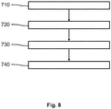
- Fig. 8 shows a schematic of a method for voltage gain.
- an input voltage signal 10 is transformed such that a first region 12 of the input voltage signal 10 is set to a first defined reference to a first operating point of an amplifier circuit.
- an input voltage signal 10 is transformed so that a second region 14 of the input voltage signal 10 is set in a second defined reference to a second operating point of the amplifier circuit.
- the first region 12 is transformed linearly to a first output signal 191.
- the second region 14 is linearly transformed to a second output signal 192.
Landscapes
- Engineering & Computer Science (AREA)
- Theoretical Computer Science (AREA)
- Power Engineering (AREA)
- Analogue/Digital Conversion (AREA)
- Amplifiers (AREA)
Applications Claiming Priority (2)
| Application Number | Priority Date | Filing Date | Title |
|---|---|---|---|
| DE102015212842.3A DE102015212842A1 (de) | 2015-07-09 | 2015-07-09 | Spannungsverstärker für einen programmierbaren Spannungsbereich |
| PCT/EP2016/065845 WO2017005743A1 (de) | 2015-07-09 | 2016-07-05 | Spannungsverstärker für einen programmierbaren spannungsbereich |
Publications (2)
| Publication Number | Publication Date |
|---|---|
| EP3320619A1 EP3320619A1 (de) | 2018-05-16 |
| EP3320619B1 true EP3320619B1 (de) | 2019-05-08 |
Family
ID=56550185
Family Applications (1)
| Application Number | Title | Priority Date | Filing Date |
|---|---|---|---|
| EP16742190.8A Active EP3320619B1 (de) | 2015-07-09 | 2016-07-05 | Spannungsverstärker für einen programmierbaren spannungsbereich |
Country Status (6)
| Country | Link |
|---|---|
| US (1) | US10340937B2 (enExample) |
| EP (1) | EP3320619B1 (enExample) |
| JP (1) | JP7120918B2 (enExample) |
| CN (1) | CN107852167B (enExample) |
| DE (1) | DE102015212842A1 (enExample) |
| WO (1) | WO2017005743A1 (enExample) |
Families Citing this family (1)
| Publication number | Priority date | Publication date | Assignee | Title |
|---|---|---|---|---|
| US12424984B2 (en) | 2021-04-14 | 2025-09-23 | Samsung Electronics Co., Ltd | Power amplification circuit including protection circuit and electronic device including power amplification circuit |
Family Cites Families (17)
| Publication number | Priority date | Publication date | Assignee | Title |
|---|---|---|---|---|
| US5231360A (en) * | 1992-06-17 | 1993-07-27 | Texas Instruments Incorporated | Multi-range voltage amplifier having multiplying digital/analog converters and programmable filter using multiplying DAC in feedback loop |
| JPH077427A (ja) * | 1993-06-18 | 1995-01-10 | Nec Corp | A/d変換装置 |
| JP3033673B2 (ja) * | 1995-04-21 | 2000-04-17 | 日本電気株式会社 | 電力増幅用の演算増幅回路 |
| FR2755325A1 (fr) * | 1996-10-25 | 1998-04-30 | Philips Electronics Nv | Dispositif de conversion analogique/numerique a caracteristique de transfert programmable |
| US6011422A (en) * | 1998-07-10 | 2000-01-04 | Delco Electronics Corporaiton | Integrated differential voltage amplifier with programmable gain and input offset voltage |
| US6522489B1 (en) * | 1999-12-21 | 2003-02-18 | Texas Instruments Incorporated | Efficient analog-to-digital converter for digital systems |
| JP3337669B2 (ja) * | 1999-12-27 | 2002-10-21 | 株式会社半導体理工学研究センター | 半導体集積回路 |
| DE60321215D1 (de) * | 2002-12-04 | 2008-07-03 | Nxp Bv | A/d-umsetzern des flash-typs |
| CN100446423C (zh) * | 2004-03-12 | 2008-12-24 | 精拓科技股份有限公司 | 能隙参考电压电路装置 |
| US7190291B2 (en) * | 2005-01-05 | 2007-03-13 | Artesyn Technologies, Inc. | Programmable error amplifier for sensing voltage error in the feedback path of digitially programmable voltage sources |
| DE102005020319B4 (de) * | 2005-05-02 | 2010-06-17 | Infineon Technologies Ag | Verstärkeranordnung mit einem umschaltbaren Verstärkungsfaktor und Verfahren zum Verstärken eines zu verstärkenden Signals mit einem umschaltbaren Verstärkungsfaktor |
| DE602005005823T2 (de) * | 2005-09-12 | 2009-05-07 | Rohde & Schwarz Gmbh & Co. Kg | Schneller Analog-Digital-Wandler |
| US7315272B2 (en) * | 2005-10-27 | 2008-01-01 | Industrial Technology Research Institute | Inverter-based flash analog-to-digital converter using floating resistor ladder |
| ATE419678T1 (de) * | 2006-02-17 | 2009-01-15 | Sicon Semiconductor Ab | Flexibler analog-digital-wandler |
| US8193962B1 (en) * | 2010-07-13 | 2012-06-05 | Sandia Corporation | High resolution A/D conversion based on piecewise conversion at lower resolution |
| US8217822B2 (en) * | 2010-11-09 | 2012-07-10 | Microsoft Corporation | Resolution enhancing analog-to-digital conversion |
| US9041570B2 (en) * | 2011-09-30 | 2015-05-26 | Nec Corporation | Analog-to-digital converter and analog-to-digital conversion method |
-
2015
- 2015-07-09 DE DE102015212842.3A patent/DE102015212842A1/de not_active Withdrawn
-
2016
- 2016-07-05 CN CN201680040673.7A patent/CN107852167B/zh not_active Expired - Fee Related
- 2016-07-05 EP EP16742190.8A patent/EP3320619B1/de active Active
- 2016-07-05 WO PCT/EP2016/065845 patent/WO2017005743A1/de not_active Ceased
- 2016-07-05 JP JP2018500547A patent/JP7120918B2/ja active Active
- 2016-07-05 US US15/742,983 patent/US10340937B2/en active Active
Non-Patent Citations (1)
| Title |
|---|
| None * |
Also Published As
| Publication number | Publication date |
|---|---|
| US10340937B2 (en) | 2019-07-02 |
| CN107852167A (zh) | 2018-03-27 |
| CN107852167B (zh) | 2021-06-29 |
| WO2017005743A1 (de) | 2017-01-12 |
| DE102015212842A1 (de) | 2017-01-12 |
| JP2018519767A (ja) | 2018-07-19 |
| EP3320619A1 (de) | 2018-05-16 |
| JP7120918B2 (ja) | 2022-08-17 |
| US20180351567A1 (en) | 2018-12-06 |
Similar Documents
| Publication | Publication Date | Title |
|---|---|---|
| DE102004039161B4 (de) | Faltender Analog/Digital-Wandler | |
| DE60311356T2 (de) | Referenzleiter mit verbesserter Rückkopplungsstabilität | |
| DE102012100144B4 (de) | Kalibrierungsschaltung und Verfahren zum Kalibrieren einer kapazitiven Kompensation in Digital-Analog-Wandlern | |
| DE60036776T2 (de) | Verstärkerschaltung | |
| DE102015108384B4 (de) | Verfahren zum Betreiben einer Leistungsversorgung und integrierte Schaltung | |
| DE102009004564B4 (de) | ADC mit energiesparender Abtastung | |
| DE60123535T2 (de) | Mehrstufenwandler mit Anwendung eines digitalen Zittersignals | |
| DE102015101837A1 (de) | Vorrichtung und Verfahren zur Verbesserung der Gleichtaktunterdrückung | |
| DE102014020062B3 (de) | Verstärkungssystem mit Digital-Analog-Wandler (DAWs) und Ausgangsstufen der DAWs | |
| DE102014113213A1 (de) | Magnetfeldsensoren und systeme mit sensorschaltungsabschnitten mit unterschiedlichen vorspannungen und frequenzbereichen | |
| DE102021128252A1 (de) | Glitch-Reduktionstechnik für Schaltverstärker mit wählbarer Übertragungsverstärkung | |
| DE69132219T2 (de) | Repetative zellenanpassungstechnik für integrierte schaltungen | |
| DE4320691A1 (de) | Digital/Analog-Wandler | |
| DE102009002062B4 (de) | Analog-Digital-Umsetzer mit breitbandigem Eingangsnetzwerk | |
| DE102004002013B4 (de) | Hochauflösender Digital-Analog-Umsetzer mit geringem Flächenbedarf | |
| DE2129383B2 (de) | Pulscodemodulator mit knickkennlinien-amplitudenwandler | |
| EP3320619B1 (de) | Spannungsverstärker für einen programmierbaren spannungsbereich | |
| EP3141877A2 (de) | Vorrichtung und verfahren zum betreiben passiver infrarotsensoren | |
| DE102021132537B3 (de) | Strommessschaltung | |
| DE102004022991B3 (de) | Abtast-Differenzverstärker und Abtast-Verstärker | |
| WO2021219167A1 (de) | Pegelumsetzer und schaltungsanordnung umfassend solche pegelumsetzer | |
| DE112018005419T5 (de) | Sensorausgangsschaltung | |
| DE4402952A1 (de) | Verfahren zur Analog - Digital - Wandlung | |
| DE10047396C1 (de) | Schaltungsanordnung zur umschaltbaren Verstärkung von Analogsignalen | |
| EP1565991B1 (de) | Analog-digital-wandler |
Legal Events
| Date | Code | Title | Description |
|---|---|---|---|
| STAA | Information on the status of an ep patent application or granted ep patent |
Free format text: STATUS: THE INTERNATIONAL PUBLICATION HAS BEEN MADE |
|
| PUAI | Public reference made under article 153(3) epc to a published international application that has entered the european phase |
Free format text: ORIGINAL CODE: 0009012 |
|
| STAA | Information on the status of an ep patent application or granted ep patent |
Free format text: STATUS: REQUEST FOR EXAMINATION WAS MADE |
|
| 17P | Request for examination filed |
Effective date: 20180209 |
|
| AK | Designated contracting states |
Kind code of ref document: A1 Designated state(s): AL AT BE BG CH CY CZ DE DK EE ES FI FR GB GR HR HU IE IS IT LI LT LU LV MC MK MT NL NO PL PT RO RS SE SI SK SM TR |
|
| AX | Request for extension of the european patent |
Extension state: BA ME |
|
| RIN1 | Information on inventor provided before grant (corrected) |
Inventor name: GREWING, CHRISTIAN |
|
| DAV | Request for validation of the european patent (deleted) | ||
| DAX | Request for extension of the european patent (deleted) | ||
| GRAP | Despatch of communication of intention to grant a patent |
Free format text: ORIGINAL CODE: EPIDOSNIGR1 |
|
| STAA | Information on the status of an ep patent application or granted ep patent |
Free format text: STATUS: GRANT OF PATENT IS INTENDED |
|
| RIC1 | Information provided on ipc code assigned before grant |
Ipc: H03M 1/18 20060101ALI20181130BHEP Ipc: H03F 3/45 20060101ALI20181130BHEP Ipc: H03M 1/12 20060101AFI20181130BHEP |
|
| INTG | Intention to grant announced |
Effective date: 20190108 |
|
| GRAS | Grant fee paid |
Free format text: ORIGINAL CODE: EPIDOSNIGR3 |
|
| GRAA | (expected) grant |
Free format text: ORIGINAL CODE: 0009210 |
|
| STAA | Information on the status of an ep patent application or granted ep patent |
Free format text: STATUS: THE PATENT HAS BEEN GRANTED |
|
| AK | Designated contracting states |
Kind code of ref document: B1 Designated state(s): AL AT BE BG CH CY CZ DE DK EE ES FI FR GB GR HR HU IE IS IT LI LT LU LV MC MK MT NL NO PL PT RO RS SE SI SK SM TR |
|
| REG | Reference to a national code |
Ref country code: GB Ref legal event code: FG4D Free format text: NOT ENGLISH |
|
| REG | Reference to a national code |
Ref country code: CH Ref legal event code: EP Ref country code: AT Ref legal event code: REF Ref document number: 1131800 Country of ref document: AT Kind code of ref document: T Effective date: 20190515 |
|
| REG | Reference to a national code |
Ref country code: DE Ref legal event code: R096 Ref document number: 502016004624 Country of ref document: DE |
|
| REG | Reference to a national code |
Ref country code: IE Ref legal event code: FG4D Free format text: LANGUAGE OF EP DOCUMENT: GERMAN |
|
| REG | Reference to a national code |
Ref country code: SE Ref legal event code: TRGR |
|
| REG | Reference to a national code |
Ref country code: NL Ref legal event code: MP Effective date: 20190508 |
|
| REG | Reference to a national code |
Ref country code: LT Ref legal event code: MG4D |
|
| PG25 | Lapsed in a contracting state [announced via postgrant information from national office to epo] |
Ref country code: NL Free format text: LAPSE BECAUSE OF FAILURE TO SUBMIT A TRANSLATION OF THE DESCRIPTION OR TO PAY THE FEE WITHIN THE PRESCRIBED TIME-LIMIT Effective date: 20190508 Ref country code: HR Free format text: LAPSE BECAUSE OF FAILURE TO SUBMIT A TRANSLATION OF THE DESCRIPTION OR TO PAY THE FEE WITHIN THE PRESCRIBED TIME-LIMIT Effective date: 20190508 Ref country code: ES Free format text: LAPSE BECAUSE OF FAILURE TO SUBMIT A TRANSLATION OF THE DESCRIPTION OR TO PAY THE FEE WITHIN THE PRESCRIBED TIME-LIMIT Effective date: 20190508 Ref country code: LT Free format text: LAPSE BECAUSE OF FAILURE TO SUBMIT A TRANSLATION OF THE DESCRIPTION OR TO PAY THE FEE WITHIN THE PRESCRIBED TIME-LIMIT Effective date: 20190508 Ref country code: NO Free format text: LAPSE BECAUSE OF FAILURE TO SUBMIT A TRANSLATION OF THE DESCRIPTION OR TO PAY THE FEE WITHIN THE PRESCRIBED TIME-LIMIT Effective date: 20190808 Ref country code: AL Free format text: LAPSE BECAUSE OF FAILURE TO SUBMIT A TRANSLATION OF THE DESCRIPTION OR TO PAY THE FEE WITHIN THE PRESCRIBED TIME-LIMIT Effective date: 20190508 Ref country code: PT Free format text: LAPSE BECAUSE OF FAILURE TO SUBMIT A TRANSLATION OF THE DESCRIPTION OR TO PAY THE FEE WITHIN THE PRESCRIBED TIME-LIMIT Effective date: 20190908 |
|
| PG25 | Lapsed in a contracting state [announced via postgrant information from national office to epo] |
Ref country code: BG Free format text: LAPSE BECAUSE OF FAILURE TO SUBMIT A TRANSLATION OF THE DESCRIPTION OR TO PAY THE FEE WITHIN THE PRESCRIBED TIME-LIMIT Effective date: 20190808 Ref country code: RS Free format text: LAPSE BECAUSE OF FAILURE TO SUBMIT A TRANSLATION OF THE DESCRIPTION OR TO PAY THE FEE WITHIN THE PRESCRIBED TIME-LIMIT Effective date: 20190508 Ref country code: LV Free format text: LAPSE BECAUSE OF FAILURE TO SUBMIT A TRANSLATION OF THE DESCRIPTION OR TO PAY THE FEE WITHIN THE PRESCRIBED TIME-LIMIT Effective date: 20190508 Ref country code: GR Free format text: LAPSE BECAUSE OF FAILURE TO SUBMIT A TRANSLATION OF THE DESCRIPTION OR TO PAY THE FEE WITHIN THE PRESCRIBED TIME-LIMIT Effective date: 20190809 |
|
| PG25 | Lapsed in a contracting state [announced via postgrant information from national office to epo] |
Ref country code: DK Free format text: LAPSE BECAUSE OF FAILURE TO SUBMIT A TRANSLATION OF THE DESCRIPTION OR TO PAY THE FEE WITHIN THE PRESCRIBED TIME-LIMIT Effective date: 20190508 Ref country code: CZ Free format text: LAPSE BECAUSE OF FAILURE TO SUBMIT A TRANSLATION OF THE DESCRIPTION OR TO PAY THE FEE WITHIN THE PRESCRIBED TIME-LIMIT Effective date: 20190508 Ref country code: SK Free format text: LAPSE BECAUSE OF FAILURE TO SUBMIT A TRANSLATION OF THE DESCRIPTION OR TO PAY THE FEE WITHIN THE PRESCRIBED TIME-LIMIT Effective date: 20190508 Ref country code: RO Free format text: LAPSE BECAUSE OF FAILURE TO SUBMIT A TRANSLATION OF THE DESCRIPTION OR TO PAY THE FEE WITHIN THE PRESCRIBED TIME-LIMIT Effective date: 20190508 Ref country code: EE Free format text: LAPSE BECAUSE OF FAILURE TO SUBMIT A TRANSLATION OF THE DESCRIPTION OR TO PAY THE FEE WITHIN THE PRESCRIBED TIME-LIMIT Effective date: 20190508 |
|
| REG | Reference to a national code |
Ref country code: DE Ref legal event code: R097 Ref document number: 502016004624 Country of ref document: DE |
|
| PG25 | Lapsed in a contracting state [announced via postgrant information from national office to epo] |
Ref country code: SM Free format text: LAPSE BECAUSE OF FAILURE TO SUBMIT A TRANSLATION OF THE DESCRIPTION OR TO PAY THE FEE WITHIN THE PRESCRIBED TIME-LIMIT Effective date: 20190508 Ref country code: MC Free format text: LAPSE BECAUSE OF FAILURE TO SUBMIT A TRANSLATION OF THE DESCRIPTION OR TO PAY THE FEE WITHIN THE PRESCRIBED TIME-LIMIT Effective date: 20190508 |
|
| PLBE | No opposition filed within time limit |
Free format text: ORIGINAL CODE: 0009261 |
|
| STAA | Information on the status of an ep patent application or granted ep patent |
Free format text: STATUS: NO OPPOSITION FILED WITHIN TIME LIMIT |
|
| PG25 | Lapsed in a contracting state [announced via postgrant information from national office to epo] |
Ref country code: TR Free format text: LAPSE BECAUSE OF FAILURE TO SUBMIT A TRANSLATION OF THE DESCRIPTION OR TO PAY THE FEE WITHIN THE PRESCRIBED TIME-LIMIT Effective date: 20190508 |
|
| 26N | No opposition filed |
Effective date: 20200211 |
|
| PG25 | Lapsed in a contracting state [announced via postgrant information from national office to epo] |
Ref country code: PL Free format text: LAPSE BECAUSE OF FAILURE TO SUBMIT A TRANSLATION OF THE DESCRIPTION OR TO PAY THE FEE WITHIN THE PRESCRIBED TIME-LIMIT Effective date: 20190508 |
|
| PG25 | Lapsed in a contracting state [announced via postgrant information from national office to epo] |
Ref country code: LU Free format text: LAPSE BECAUSE OF NON-PAYMENT OF DUE FEES Effective date: 20190705 Ref country code: SI Free format text: LAPSE BECAUSE OF FAILURE TO SUBMIT A TRANSLATION OF THE DESCRIPTION OR TO PAY THE FEE WITHIN THE PRESCRIBED TIME-LIMIT Effective date: 20190508 |
|
| PG25 | Lapsed in a contracting state [announced via postgrant information from national office to epo] |
Ref country code: IE Free format text: LAPSE BECAUSE OF NON-PAYMENT OF DUE FEES Effective date: 20190705 |
|
| PG25 | Lapsed in a contracting state [announced via postgrant information from national office to epo] |
Ref country code: CY Free format text: LAPSE BECAUSE OF FAILURE TO SUBMIT A TRANSLATION OF THE DESCRIPTION OR TO PAY THE FEE WITHIN THE PRESCRIBED TIME-LIMIT Effective date: 20190508 |
|
| PG25 | Lapsed in a contracting state [announced via postgrant information from national office to epo] |
Ref country code: IS Free format text: LAPSE BECAUSE OF FAILURE TO SUBMIT A TRANSLATION OF THE DESCRIPTION OR TO PAY THE FEE WITHIN THE PRESCRIBED TIME-LIMIT Effective date: 20190908 |
|
| PG25 | Lapsed in a contracting state [announced via postgrant information from national office to epo] |
Ref country code: MT Free format text: LAPSE BECAUSE OF FAILURE TO SUBMIT A TRANSLATION OF THE DESCRIPTION OR TO PAY THE FEE WITHIN THE PRESCRIBED TIME-LIMIT Effective date: 20190508 Ref country code: HU Free format text: LAPSE BECAUSE OF FAILURE TO SUBMIT A TRANSLATION OF THE DESCRIPTION OR TO PAY THE FEE WITHIN THE PRESCRIBED TIME-LIMIT; INVALID AB INITIO Effective date: 20160705 |
|
| PG25 | Lapsed in a contracting state [announced via postgrant information from national office to epo] |
Ref country code: MK Free format text: LAPSE BECAUSE OF FAILURE TO SUBMIT A TRANSLATION OF THE DESCRIPTION OR TO PAY THE FEE WITHIN THE PRESCRIBED TIME-LIMIT Effective date: 20190508 |
|
| PGFP | Annual fee paid to national office [announced via postgrant information from national office to epo] |
Ref country code: SE Payment date: 20220721 Year of fee payment: 7 Ref country code: IT Payment date: 20220729 Year of fee payment: 7 Ref country code: GB Payment date: 20220725 Year of fee payment: 7 Ref country code: FI Payment date: 20220719 Year of fee payment: 7 Ref country code: DE Payment date: 20220621 Year of fee payment: 7 Ref country code: AT Payment date: 20220718 Year of fee payment: 7 |
|
| PGFP | Annual fee paid to national office [announced via postgrant information from national office to epo] |
Ref country code: FR Payment date: 20220725 Year of fee payment: 7 Ref country code: BE Payment date: 20220720 Year of fee payment: 7 |
|
| PGFP | Annual fee paid to national office [announced via postgrant information from national office to epo] |
Ref country code: CH Payment date: 20220727 Year of fee payment: 7 |
|
| P01 | Opt-out of the competence of the unified patent court (upc) registered |
Effective date: 20230523 |
|
| REG | Reference to a national code |
Ref country code: DE Ref legal event code: R119 Ref document number: 502016004624 Country of ref document: DE |
|
| REG | Reference to a national code |
Ref country code: CH Ref legal event code: PL |
|
| REG | Reference to a national code |
Ref country code: SE Ref legal event code: EUG |
|
| REG | Reference to a national code |
Ref country code: AT Ref legal event code: MM01 Ref document number: 1131800 Country of ref document: AT Kind code of ref document: T Effective date: 20230705 |
|
| REG | Reference to a national code |
Ref country code: BE Ref legal event code: MM Effective date: 20230731 |
|
| GBPC | Gb: european patent ceased through non-payment of renewal fee |
Effective date: 20230705 |
|
| PG25 | Lapsed in a contracting state [announced via postgrant information from national office to epo] |
Ref country code: AT Free format text: LAPSE BECAUSE OF NON-PAYMENT OF DUE FEES Effective date: 20230705 |
|
| PG25 | Lapsed in a contracting state [announced via postgrant information from national office to epo] |
Ref country code: FI Free format text: LAPSE BECAUSE OF NON-PAYMENT OF DUE FEES Effective date: 20230705 Ref country code: DE Free format text: LAPSE BECAUSE OF NON-PAYMENT OF DUE FEES Effective date: 20240201 Ref country code: AT Free format text: LAPSE BECAUSE OF NON-PAYMENT OF DUE FEES Effective date: 20230705 Ref country code: CH Free format text: LAPSE BECAUSE OF NON-PAYMENT OF DUE FEES Effective date: 20230731 Ref country code: GB Free format text: LAPSE BECAUSE OF NON-PAYMENT OF DUE FEES Effective date: 20230705 |
|
| PG25 | Lapsed in a contracting state [announced via postgrant information from national office to epo] |
Ref country code: SE Free format text: LAPSE BECAUSE OF NON-PAYMENT OF DUE FEES Effective date: 20230706 Ref country code: FR Free format text: LAPSE BECAUSE OF NON-PAYMENT OF DUE FEES Effective date: 20230731 Ref country code: BE Free format text: LAPSE BECAUSE OF NON-PAYMENT OF DUE FEES Effective date: 20230731 |
|
| PG25 | Lapsed in a contracting state [announced via postgrant information from national office to epo] |
Ref country code: IT Free format text: LAPSE BECAUSE OF NON-PAYMENT OF DUE FEES Effective date: 20230705 |