EP3306381B1 - Optisches halbleitermodulationselement - Google Patents
Optisches halbleitermodulationselement Download PDFInfo
- Publication number
- EP3306381B1 EP3306381B1 EP16802809.0A EP16802809A EP3306381B1 EP 3306381 B1 EP3306381 B1 EP 3306381B1 EP 16802809 A EP16802809 A EP 16802809A EP 3306381 B1 EP3306381 B1 EP 3306381B1
- Authority
- EP
- European Patent Office
- Prior art keywords
- type
- layer
- clad layer
- type clad
- semiconductor
- Prior art date
- Legal status (The legal status is an assumption and is not a legal conclusion. Google has not performed a legal analysis and makes no representation as to the accuracy of the status listed.)
- Active
Links
Images






Classifications
-
- G—PHYSICS
- G02—OPTICS
- G02F—OPTICAL DEVICES OR ARRANGEMENTS FOR THE CONTROL OF LIGHT BY MODIFICATION OF THE OPTICAL PROPERTIES OF THE MEDIA OF THE ELEMENTS INVOLVED THEREIN; NON-LINEAR OPTICS; FREQUENCY-CHANGING OF LIGHT; OPTICAL LOGIC ELEMENTS; OPTICAL ANALOGUE/DIGITAL CONVERTERS
- G02F1/00—Devices or arrangements for the control of the intensity, colour, phase, polarisation or direction of light arriving from an independent light source, e.g. switching, gating or modulating; Non-linear optics
- G02F1/01—Devices or arrangements for the control of the intensity, colour, phase, polarisation or direction of light arriving from an independent light source, e.g. switching, gating or modulating; Non-linear optics for the control of the intensity, phase, polarisation or colour
- G02F1/21—Devices or arrangements for the control of the intensity, colour, phase, polarisation or direction of light arriving from an independent light source, e.g. switching, gating or modulating; Non-linear optics for the control of the intensity, phase, polarisation or colour by interference
- G02F1/225—Devices or arrangements for the control of the intensity, colour, phase, polarisation or direction of light arriving from an independent light source, e.g. switching, gating or modulating; Non-linear optics for the control of the intensity, phase, polarisation or colour by interference in an optical waveguide structure
- G02F1/2257—Devices or arrangements for the control of the intensity, colour, phase, polarisation or direction of light arriving from an independent light source, e.g. switching, gating or modulating; Non-linear optics for the control of the intensity, phase, polarisation or colour by interference in an optical waveguide structure the optical waveguides being made of semiconducting material
-
- G—PHYSICS
- G02—OPTICS
- G02F—OPTICAL DEVICES OR ARRANGEMENTS FOR THE CONTROL OF LIGHT BY MODIFICATION OF THE OPTICAL PROPERTIES OF THE MEDIA OF THE ELEMENTS INVOLVED THEREIN; NON-LINEAR OPTICS; FREQUENCY-CHANGING OF LIGHT; OPTICAL LOGIC ELEMENTS; OPTICAL ANALOGUE/DIGITAL CONVERTERS
- G02F1/00—Devices or arrangements for the control of the intensity, colour, phase, polarisation or direction of light arriving from an independent light source, e.g. switching, gating or modulating; Non-linear optics
- G02F1/01—Devices or arrangements for the control of the intensity, colour, phase, polarisation or direction of light arriving from an independent light source, e.g. switching, gating or modulating; Non-linear optics for the control of the intensity, phase, polarisation or colour
- G02F1/015—Devices or arrangements for the control of the intensity, colour, phase, polarisation or direction of light arriving from an independent light source, e.g. switching, gating or modulating; Non-linear optics for the control of the intensity, phase, polarisation or colour based on semiconductor elements having potential barriers, e.g. having a PN or PIN junction
- G02F1/025—Devices or arrangements for the control of the intensity, colour, phase, polarisation or direction of light arriving from an independent light source, e.g. switching, gating or modulating; Non-linear optics for the control of the intensity, phase, polarisation or colour based on semiconductor elements having potential barriers, e.g. having a PN or PIN junction in an optical waveguide structure
-
- G—PHYSICS
- G02—OPTICS
- G02F—OPTICAL DEVICES OR ARRANGEMENTS FOR THE CONTROL OF LIGHT BY MODIFICATION OF THE OPTICAL PROPERTIES OF THE MEDIA OF THE ELEMENTS INVOLVED THEREIN; NON-LINEAR OPTICS; FREQUENCY-CHANGING OF LIGHT; OPTICAL LOGIC ELEMENTS; OPTICAL ANALOGUE/DIGITAL CONVERTERS
- G02F1/00—Devices or arrangements for the control of the intensity, colour, phase, polarisation or direction of light arriving from an independent light source, e.g. switching, gating or modulating; Non-linear optics
- G02F1/01—Devices or arrangements for the control of the intensity, colour, phase, polarisation or direction of light arriving from an independent light source, e.g. switching, gating or modulating; Non-linear optics for the control of the intensity, phase, polarisation or colour
- G02F1/21—Devices or arrangements for the control of the intensity, colour, phase, polarisation or direction of light arriving from an independent light source, e.g. switching, gating or modulating; Non-linear optics for the control of the intensity, phase, polarisation or colour by interference
- G02F1/225—Devices or arrangements for the control of the intensity, colour, phase, polarisation or direction of light arriving from an independent light source, e.g. switching, gating or modulating; Non-linear optics for the control of the intensity, phase, polarisation or colour by interference in an optical waveguide structure
-
- G—PHYSICS
- G02—OPTICS
- G02F—OPTICAL DEVICES OR ARRANGEMENTS FOR THE CONTROL OF LIGHT BY MODIFICATION OF THE OPTICAL PROPERTIES OF THE MEDIA OF THE ELEMENTS INVOLVED THEREIN; NON-LINEAR OPTICS; FREQUENCY-CHANGING OF LIGHT; OPTICAL LOGIC ELEMENTS; OPTICAL ANALOGUE/DIGITAL CONVERTERS
- G02F1/00—Devices or arrangements for the control of the intensity, colour, phase, polarisation or direction of light arriving from an independent light source, e.g. switching, gating or modulating; Non-linear optics
- G02F1/01—Devices or arrangements for the control of the intensity, colour, phase, polarisation or direction of light arriving from an independent light source, e.g. switching, gating or modulating; Non-linear optics for the control of the intensity, phase, polarisation or colour
- G02F1/21—Devices or arrangements for the control of the intensity, colour, phase, polarisation or direction of light arriving from an independent light source, e.g. switching, gating or modulating; Non-linear optics for the control of the intensity, phase, polarisation or colour by interference
- G02F1/212—Mach-Zehnder type
-
- G—PHYSICS
- G02—OPTICS
- G02F—OPTICAL DEVICES OR ARRANGEMENTS FOR THE CONTROL OF LIGHT BY MODIFICATION OF THE OPTICAL PROPERTIES OF THE MEDIA OF THE ELEMENTS INVOLVED THEREIN; NON-LINEAR OPTICS; FREQUENCY-CHANGING OF LIGHT; OPTICAL LOGIC ELEMENTS; OPTICAL ANALOGUE/DIGITAL CONVERTERS
- G02F2202/00—Materials and properties
- G02F2202/10—Materials and properties semiconductor
- G02F2202/102—In×P and alloy
-
- G—PHYSICS
- G02—OPTICS
- G02F—OPTICAL DEVICES OR ARRANGEMENTS FOR THE CONTROL OF LIGHT BY MODIFICATION OF THE OPTICAL PROPERTIES OF THE MEDIA OF THE ELEMENTS INVOLVED THEREIN; NON-LINEAR OPTICS; FREQUENCY-CHANGING OF LIGHT; OPTICAL LOGIC ELEMENTS; OPTICAL ANALOGUE/DIGITAL CONVERTERS
- G02F2202/00—Materials and properties
- G02F2202/10—Materials and properties semiconductor
- G02F2202/107—Zn×S or Zn×Se and alloys
Definitions
- the present invention relates to a semiconductor optical modulation element that functions as a high-speed optical modulator in the optical communication field.
- MZ optical modulators are exemplified as important element devices that involve in those characteristics, and many researches and developments thereof have been promoted.
- an attention is specially focused on optical modulators using compound semiconductor materials including InP from optical modulators using lithium niobate (LN) as a material.
- compound semiconductor optical modulators In order to cause the compound semiconductor optical modulator to operate as an optical modulator, the interaction between electricity (electric field) and propagation light is utilized.
- the strong interaction between light and electricity is achieved by using a core layer that generally traps the light as a non-doped layer, sandwiching the core layer between p-type and n-type clad layers in the order from the top layer, and applying a reverse bias voltage thereto.
- the p-type semiconductor used herein has a higher electrical resistivity and a higher optical absorption of material, than the n-type semiconductor, by approximately one or more order of magnitude, so that there are large problems in achieving higher-speed modulation operation and lower optical loss.
- a contact area between the p-type semiconductor and an electrode is sufficiently small compared with that of the n-type, so that the increase in contact resistance causes further degradation of modulation bandwidth.
- a semiconductor optical modulation element having a cross-sectional structure as illustrated in Fig. 1 was proposed in the past (for example, Patent Literatures 1 and 2).
- the semiconductor optical modulation element illustrated in Fig. 1 has a waveguide structure of a deep-ridge or high-mesa shape that is stacked on a substrate 10.
- the high-mesa waveguide is used in Fig. 1 , this is a configuration generally employed in a semiconductor MZ modulator for strengthening the interaction between light and electricity and reducing the parasitic capacitance.
- a signal electrode 16 is provided on the waveguide structure via an n-type contact layer 15.
- a ground electrode 17 is provided on an n-type clad layer 11.
- npin type optical modulator in which clad layers 11 and 14 above and below a non-doped layer 12 are served as the n-type, a thin p-type layer serving as a carrier block layer 13 for suppressing the electron current between the both n layers is inserted.
- This npin type does not use a p-type clad that has large optical loss, thereby making it possible to use a relatively long waveguide.
- the npin type is easy to simultaneously satisfy the reduction in drive voltage and the velocity match between a microwave and light wave because of the flexibility in which the thickness of a depletion layer can be appropriately designed as desired, and thus has an advantage to increase the response speed of the modulator.
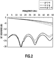
- the RF responses calculated by calculation simulation in the npin layer structure is illustrated in Fig. 2 .
- the npin type modulator having a high-mesa shape as is in Fig. 1 involves the large variation in electric surge resistance and the instability of modulation operation, as problems.
- the main factor of the variation in surge resistance is considered to be in that the damage along with the waveguide side walls caused by dry etching processing lowers the function as a carrier block layer of the p-type semiconductor.
- the instability of modulation operation has specifically problems including generation of the incident light power dependence of the modulation efficiency, generation of the bias voltage dependence of the modulation efficiency, and the lowering of the resisting pressure. It can be considered that the main factor of this is in that hole carriers are concentrated and accumulated on the p layer in the high-mesa waveguide.
- Patent Literatures 3 and 4 various proposals with respect to these problems have been made (Patent Literatures 3 and 4), all of these proposals require complicated structures and the optimization of the material resistance, so that many problems as a practical device thus remain. As a result, in the current research and development, the most of research institutes employ the conventional pin structure from the viewpoint of the electrical stability (Non Patent Literature 1).
- EA type modulators of a nip structure in which an upper layer clad is of n-type, a lower layer clad and a substrate are of p-type for reduction in contact resistance have been proposed (Patent Literature 5) .
- the EA modulator generally has an electrode structure of a lumped constant type, and thus does not need to satisfy the characteristic impedance, the velocity matching between a light wave and microwave, and the like.
- the MZ modulator having an electrode length longer by approximately one order of magnitude than that of the EA modulator, it cannot be said that simply reversing the semiconductor layer structure is not sufficient for the improvement in the modulation bandwidth.
- a cross-sectional structure as illustrated in Fig. 3 has been proposed (for example, Non Patent Literature 1).
- a capacitance- loaded electrode structure is employed in Fig. 3 , in which a coplanar-strip line including electrodes with large cross-sectional areas is used as a main line, and a lumped constant electrode (capacitance) which is separated in a length sufficiently shorter than the micro wave is added on an optical waveguide.
- a signal electrode 16 and a ground electrode 17 are provided on a p-type clad layer 19 via a p-type contact layer 20.
- NPL 1 R. Kaiser, et al. "High Performance Travelling Wave Mach-Zehnder Modulators for Emerging Generations of High Capacity Transmitter Components" International Conference on. Transparent Optical Networks ICTON 2013, We. D2.2
- the electrode structure illustrated in Fig. 3 is only applied to a semiconductor element having the pin structure from the top layer, but has not reached an ultimate high-speed modulation operation by optimizing both of the semiconductor layer and the electrode structure.
- the waveguide is formed in the [0 ⁇ 1] plane direction, a dry etching process needs to be used for vertical etching processing of the clad layer in the upper portion as is in Fig. 3 .
- the number represented by an asterisk (*) means "1 with overbar".
- the problems of the electrical surge and the unstable operation remain in the high-mesa waveguide type optical modulation element of the npin layer structure, and the conventional capacitance- loaded type optical modulation element with the negative effect to the high-speed operation due to the upper p-type clad layer having the high contact resistance and material resistance is requested to have the high processing accuracy when the ridge waveguide is processed.
- the present invention is made in view of the abovementioned conventional problems, and an object of the present invention is to provide a Mach-Zehnder (MZ) type semiconductor optical modulation element that can be used as a modulator that is ultrafast and excellent in electrical stability.
- MZ Mach-Zehnder
- Fig. 4 is a plan view of a semiconductor optical modulation element in the present invention
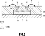
- Fig. 5 is a cross-sectional view of a refractive index modulation region (V-V) of the semiconductor optical modulation element
- Fig. 6 is a cross-sectional view of an input and output region (VI-VI), where the refractive index of the light is not modulated, of the semiconductor optical modulation element.
- the refractive index modulation region indicates a region where applying electric signals to have a core layer causes a secondary optical effect therein, thereby modulating the refractive index in the core layer.
- the semiconductor optical modulation element of the present invention is configured as a Mach-Zehnder type optical waveguide L in which a capacitance- loaded type traveling-wave electrode pattern P is formed on an upper surface thereof, as illustrated in Fig. 4 .
- the optical waveguide is, as illustrated in Fig. 4 , a semiconductor optical modulation element of a Mach-Zehnder type that performs modulation of light using a refractive index modulation region where the refractive index of the light guided to an optical waveguide is modulated and an input and output region where multiplexing/demultiplexing of the light split in the refractive index modulation region is performed, and the optical waveguide is provided with a configuration in which, in the refractive index modulation region thereof, on a substrate surface equivalent to a (100) plane of a sphalerite-type semi-insulating semiconductor crystal substrate 10, an n-type clad layer 14, an i core layer 12, and a p-type clad layer 19 are stacked in the order from the top layer, the n-type clad layer 14 is formed in a ridge shape in an inverted mesa direction, and a capacitance- loaded electrode is provided on the n-type clad layer 14.
- a semi-insulating InP clad layer 22 in a portion of the optical waveguide where the refractive index of the light is not modulated, a semi-insulating InP clad layer 22, the i core layer 12, and the p-type clad layer 19 are stacked in the order from the top layer on the substrate surface equivalent to the (100) plane of the sphalerite-type semi-insulating semiconductor crystal substrate 10.
- the sphalerite-type semi-insulating semiconductor crystal substrate 10 for example, an InP substrate can be used.
- the n-type clad layer 14 in a portion where the refractive index of the light is not modulated is removed and the removed part is backfilled with the semi-insulating InP clad layer 22, and thereafter the clad layer is subjected to etching of a Mach-Zehnder waveguide shape in a direction equivalent to a [011] plane direction, thereby the clad layer of the optical modulation waveguide can be formed in a ridge shape in the inverted mesa direction.
- a capacitance- loaded type electrode structure can be formed on an upper surface of the n-type clad layer 14.
- the clad layers 14, 22 are subjected to etching of a Mach-Zehnder waveguide shape in the direction equivalent to the [011] plane direction, so that the clads 14, 22 of the optical modulation waveguide are formed in a ridge shape in the inverted mesa direction.
- the capacitance- loaded type electrode structure is provided in such a manner that a signal electrode 16 and a ground electrode 17 are formed on the upper surface of the n-type clad layer 14 via the n-type contact layer 15, and the signal electrode 16 or the ground electrode 17 is electrically connected to a signal electrode 16 or a ground electrode 17 provided on the insulating layer at both sides of the waveguide via bonding wires w.
- the capacitance- loaded electrode can be connected to a differential signal source via a differential line wiring board.
- the p-type clad layer 19 is brought into contact with an electrode 23 that is connected to a power source, via a p-type contact layer 21.
- the semiconductor optical modulation element illustrated in Figs. 4 , 5 , and 6 generates a secondary electric optical effect in the i core layer 12, thereby modulating the refractive index, and modulating light guided to the Mach-Zehnder type optical waveguide.
- the waveguide mesa upper portion (upper layer of the core) with a small contact area with the electrode is formed not a p-type but n-type clad. This reduces the contact resistance by approximately one order of magnitude from the conventional one.
- the waveguide stripe direction (waveguide longitudinal direction) is made to be equivalent to the [011] plane direction, and the insulating layer is etched in the inverted mesa direction.
- the p-type clad layer thickness having a bulk material resistance larger than that of the n-type is thin-filmed, and the core layer and the thin-film p layer are vertically sandwiched between the n-type clad layers, thereby ultimately reducing the semiconductor resistance and providing the high-speed modulator.
- the electrode is brought into contact with the p-type semiconductor on which hole carriers are accumulated, and the accumulated carrier are extracted.
- the present invention can form a semiconductor optical element that is used as a high-speed modulator having the electrical surge resistance by employing the ridge structure waveguide in the modulation region while assuring the high-speed operation due to the contact resistance reduction and the thinned p-type clad layer (low resistant). Moreover, holes accumulated on the p-type layer are diffused to a slab waveguide side, which is outside of a light propagation region, in the ridge structure, thereby making it possible to lower the hole concentration per unit volume compared with that of the high-mesa waveguide structure. Moreover, further lowering of the hole concentration can be expected by making these p-type layers conduct to the electrode connected to the power source. As a result, the unstable modulation operation is suppressed.
- the p-type layer is deposited to the lower layer of the non-doped layer (nip and nipn structures), these devices are subjected to etching in a direction equivalent to the [011] plane direction and the n-type clad layer is backfilled to form the clad of the optical modulation waveguide so as to be a ridge shape in the inverted mesa direction, thereby easily forming the ridge waveguide by wet etching, which results in the improvement in the controllability of the ridge shape processing and the electrical stability of the waveguide surface, compared with a case of only dry etching processing.
- an optical semiconductor element having cross sections illustrated in Figs. 5 and 6 was prepared.
- a semiconductor optical modulation element in the present example has a nip-type configuration.
- the n-type contact layer 15, the n-type clad layer 14, the non-doped clad core layer 12, the p-type clad 19, and the p-type contact layer 21 are successively stacked in this order from the top layer on the substrate 10.
- the upper layer n-type contact layer 15 includes InGaAs having a carrier concentration of 5E+18 cm -3
- the n-type clad layer 14 includes InP having a carrier concentration of 1E+18 cm -3
- the carrier concentration of the p-type InP clad layer 19 is set to 5E+17 to 1E+18 cm -3 in view of the light absorption coefficient and the electrical resistivity.
- InGaAs in which hole carriers were doped 5E+18 cm -3 or more was used. Note that, the InGaAsP layer 15 was inserted as the topmost layer of the non-doped layer 12 for utilizing the selectivity with the InP n-type clad layer 14 in the wet etching.
- the crystal growth was deposited on the semi-insulating InP (100) substrate 10 by the Metal Organic Vapor Phase Epitaxy (MOVPE).
- the band gap wavelength of the core layer 12, which is the operation light wavelength, is determined within a range in which an electric optical effect is caused to effectively act with high efficiency and the light absorption causes no problem. For example, in a case of 1.55 micron band, the light-emitting wave length of the core layer 12 is set to about 1.4 micron meters.
- the core layer 12 is preferably caused to form in the multiple quantum well structure of InGaAlAs/InAlAs in the viewpoint of the high efficiency modulation, and it is apparent that the advantage by the present invention be not lost with the multiple structure of InGaAsP/InP or InGaAsP/InGaAsP, for example.
- the compositions of the contact layers 15, 21 and the clad layers 14, 19 are not limited to the above described, and using the InGaAsP composition, for example, causes no problem.
- the upper n-type clad layer 14 in a region where the refractive index of the light is not modulated is removed by dry etching and wet etching, for the purpose of electric isolation between the elements. Moreover, from the viewpoint of the optical loss reduction, the removed part is backfilled with the semi-insulating InP 22.
- an MZ interferometer waveguide pattern including SiO 2 formed in a direction equivalent to the [011] plane direction is formed, and an optical waveguide of a ridge shape is formed in the inverted mesa direction by dry etching and wet etching processing.
- the n-type contact layer 15 and a part of the n-type clad layer 14 are subjected to dry etching
- the n-type clad layer 14 is subjected to wet etching, thereby forming the optical waveguide of a ridge shape in the inverted mesa direction.
- BCB Benzocyclobutene
- a capacitance- loaded type traveling-wave electrode pattern P as illustrated in Fig. 4 is formed by a gold plating method. Note that, using a polyimide or the like, that is the insulating low refractive index material, other than BCB, causes no problem.
- the modulator For driving the created semiconductor optical element as a modulator, after a predetermined bias is caused to apply to the DC bias electrode 23 such that the reverse direction electric field is applied to a pn junction, a high frequency signal is fed to a signal electrode (coplanar strip line).
- a signal electrode coplanar strip line
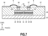
- Figs. 7 and 8 are views illustrating cross sections of a semiconductor optical modulation element according to an example 2 of the present invention.
- Fig. 7 is a cross-sectional view of V-V in Fig. 4
- Fig. 8 is a cross-sectional view of VI-VI in Fig. 4 .
- the semiconductor optical modulation element in the present example has a nipn-type configuration.
- the n-type contact layer 15 , the n-type clad layer 14, the non-doped clad core layer 12, a p-type carrier block layer 25, the n-type contact 24, and the n-type clad layer 11 are stacked in this order on the substrate 10.
- the upper layer n-type contact layer 15 includes InGaAs having a carrier concentration of 5E+18 cm -3
- the n-type clad layer 14 includes InP having a carrier concentration of 1E+18 cm -3
- hole carriers of 1E+18cm -3 are doped to InAlAs having a large band gap such that the p-type carrier block layer 25 becomes a sufficient barrier with respect to electrons.
- the InGaAsP layer 15 was inserted as the topmost layer of the non-doped layer for utilizing the selectivity with the InP n-type clad layer 14 in the wet etching.
- the crystal growth was deposited on the semi-insulating InP (100) substrate 10 by the Metal Organic Vapor Phase Epitaxy (MOVPE).
- the band gap wavelength of the core layer 12, which is the operation light wavelength, is determined within a range in which an electric optical effect is caused to effectively act with high efficiency and the light absorption causes no problem. For example, in a case of 1.55 micron band, the light-emitting wave length of the core layer 12 is set to about 1.4 micron meters.
- the core layer 12 is preferably caused to form in the multiple quantum well structure of InGaAlAs/InAlAs in the viewpoint of the high efficiency modulation, and it is apparent that the advantage by the present invention be not lost with the multiple structure of InGaAsP/InP or InGaAsP/InGaAsP, for example.
- the composition of the contact clad carrier block layer 13 is not limited to the abovementioned, but the InGaAsP composition, for example, may be used.
- the upper n-type clad layer 14 in a region where the refractive index of the light is not modulated is removed by dry etching and wet etching, for the purpose of electric isolation between the elements. Moreover, from the viewpoint of the optical loss reduction, the removed part is backfilled with the semi-insulating InP 22.
- an MZ interferometer waveguide pattern including SiO 2 formed in a direction equivalent to the [011] plane direction is formed, and an optical waveguide of a ridge shape is formed by dry etching and wet etching processing.
- BCB Benzocyclobutene
- a capacitance- loaded type traveling-wave electrode pattern P as illustrated in Fig. 4 is formed by a gold plating method. Note that, using a polyimide or the like, that is the insulating low refractive index material, other than BCB, causes no problem.
- the modulator For driving the created semiconductor optical element as a modulator, after a predetermined bias is caused to apply to the DC bias electrode 23 such that the reverse direction electric field is applied to a pn junction, a high frequency signal is fed to a signal electrode (coplanar strip line).
- a signal electrode coplanar strip line
Landscapes
- Physics & Mathematics (AREA)
- Nonlinear Science (AREA)
- General Physics & Mathematics (AREA)
- Optics & Photonics (AREA)
- Optical Modulation, Optical Deflection, Nonlinear Optics, Optical Demodulation, Optical Logic Elements (AREA)
Claims (4)
- Halbleiteroptikmodulationsbauelement einer Mach-Zehnder-Art, das eine Modulation von Licht unter Verwendung eines Brechungsindexmodulationsgebietes, in dem ein Brechungsindex des zu einem optischen Wellenleiter geführten Lichts moduliert wird, und eines Eingabe- und Ausgabegebietes durchführt, in dem ein Multiplexen/Demultiplexen des in dem Brechungsindexmodulationsgebiet aufgespaltenen Lichts durchgeführt wird,wobei in dem Brechungsindexmodulationsgebiet der optische Wellenleiter auf einer zu einer [100]-Ebene äquivalenten Substratoberfläche eines Sphalerit-artigen halbisolierenden Halbleiterkristallsubstrats (10) aus einer Halbleitermehrschichtstruktur mit zumindest einer n-Mantelschicht (14), einer i-Kernschicht (12), einer p-Mantelschicht (19) und einer n-Mantelschicht (11) von einer obersten Schicht her in Richtung der Substratoberfläche aufeinanderfolgend ausgebildet ist,die n-Mantelschicht (14) einem Ätzen in einer Richtung, die zu einer Richtung einer [011]-Ebene äquivalent ist, in eine Mach-Zehnder-Wellenleiterform unterzogen wird, und somit derart ausgebildet ist, dass sie eine Rückenform in der Richtung einer invertierten Mesa aufweist, eine kapazitätsbeladene Elektrode (10, 17) auf der n-Mantelschicht (14) bereitgestellt ist, unddadurch gekennzeichnet ist, dassdie p-Mantelschicht in einer Plattenform vorliegt, die breiter als die Rückenform ist.
- Halbleiteroptikmodulationsbauelement nach Anspruch 1, dadurch gekennzeichnet, dass in einem Abschnitt des optischen Wellenleiters, in dem der Brechungsindex des Lichts nicht moduliert wird, zumindest eine halbleitende InP-Mantelschicht (22), die i-Kernschicht (12) und die p-Mantelschicht (19) von der obersten Schicht her in Richtung der Substratoberfläche auf der zu der [100]-Ebene äquivalenten Substratoberfläche des Sphalerit-artigen halbisolierenden Halbleiterkristallsubstrats (10) gestapelt sind.
- Halbleiteroptikmodulationsbauelement nach Anspruch 1, dadurch gekennzeichnet, dass die p-Mantelschicht (13) mit einer Elektrode elektrisch in Kontakt gebracht ist, die mit einer Leistungsquelle verbunden ist.
- Halbleiteroptikmodulationsbauelement nach Anspruch 1, dadurch gekennzeichnet, dass die kapazitätsbeladene Elektrode (10, 17) mittels einer Differentialleitungs-Leiterplatte (P) mit einer differentiellen Signalquelle verbunden ist.
Applications Claiming Priority (2)
| Application Number | Priority Date | Filing Date | Title |
|---|---|---|---|
| JP2015112448 | 2015-06-02 | ||
| PCT/JP2016/002649 WO2016194369A1 (ja) | 2015-06-02 | 2016-06-01 | 半導体光変調素子 |
Publications (3)
| Publication Number | Publication Date |
|---|---|
| EP3306381A1 EP3306381A1 (de) | 2018-04-11 |
| EP3306381A4 EP3306381A4 (de) | 2019-01-09 |
| EP3306381B1 true EP3306381B1 (de) | 2020-01-29 |
Family
ID=57440465
Family Applications (1)
| Application Number | Title | Priority Date | Filing Date |
|---|---|---|---|
| EP16802809.0A Active EP3306381B1 (de) | 2015-06-02 | 2016-06-01 | Optisches halbleitermodulationselement |
Country Status (7)
| Country | Link |
|---|---|
| US (1) | US10254624B2 (de) |
| EP (1) | EP3306381B1 (de) |
| JP (1) | JP6458143B2 (de) |
| CN (1) | CN107615140B (de) |
| CA (1) | CA2988051C (de) |
| TW (1) | TWI638464B (de) |
| WO (1) | WO2016194369A1 (de) |
Families Citing this family (23)
| Publication number | Priority date | Publication date | Assignee | Title |
|---|---|---|---|---|
| US10534204B2 (en) | 2017-11-03 | 2020-01-14 | International Business Machines Corporation | Structured photorefractive layer stack |
| CN111373312B (zh) * | 2017-11-30 | 2023-08-04 | 三菱电机株式会社 | 半导体光调制器 |
| JP7247120B2 (ja) * | 2018-02-08 | 2023-03-28 | 古河電気工業株式会社 | 光集積素子および光モジュール |
| WO2019155679A1 (ja) * | 2018-02-09 | 2019-08-15 | 三菱電機株式会社 | 光半導体素子およびその製造方法 |
| DE112018007107B4 (de) * | 2018-02-19 | 2023-09-28 | Mitsubishi Electric Corporation | Optische integrierte Halbleitervorrichtung |
| CN108681111B (zh) * | 2018-03-29 | 2021-07-13 | 北京航天时代光电科技有限公司 | 一种铌酸锂电光调制器 |
| GB2580163B (en) * | 2018-12-21 | 2023-01-04 | Lumentum Tech Uk Limited | Biasing method for InP Mach-Zehnder modulators directly coupled to RF driver circuits |
| JP7139965B2 (ja) * | 2019-01-16 | 2022-09-21 | 日本電信電話株式会社 | 半導体マッハツェンダ光変調器 |
| WO2020245618A2 (zh) * | 2019-05-20 | 2020-12-10 | 华为技术(美国)有限公司 | 种电光调制器、光器件及光模块 |
| CN114365034B (zh) * | 2019-09-12 | 2025-10-14 | 恩梯梯株式会社 | 半导体Mach-Zehnder光调制器及IQ调制器 |
| CN110989215B (zh) * | 2019-12-23 | 2022-07-01 | 武汉邮电科学研究院有限公司 | 一种差分铌酸锂调制器 |
| JP7547779B2 (ja) * | 2020-05-15 | 2024-09-10 | 富士通オプティカルコンポーネンツ株式会社 | 光デバイス、及びこれを用いた光送受信機 |
| CN116097156A (zh) * | 2020-08-13 | 2023-05-09 | 华为技术有限公司 | 用于膜调制器设备的设计和制造方法 |
| US20220066280A1 (en) * | 2020-08-25 | 2022-03-03 | Sumitomo Electric Industries, Ltd. | Optical modulator |
| US11543728B2 (en) * | 2021-04-09 | 2023-01-03 | Aloe Semiconductor Inc. | High-gain differential electro-optic modulator |
| JP2022187147A (ja) * | 2021-06-07 | 2022-12-19 | 住友電気工業株式会社 | 光変調器 |
| JP7632101B2 (ja) * | 2021-06-11 | 2025-02-19 | 住友電気工業株式会社 | 光変調器及び光変調器の製造方法 |
| KR102701775B1 (ko) * | 2021-09-08 | 2024-09-03 | 한국전자통신연구원 | 쉘로우 릿지 도파로 구조를 갖는 마흐-젠더 간섭계형 광 변조기 및 그의 제조 방법 |
| WO2023095261A1 (ja) * | 2021-11-25 | 2023-06-01 | 三菱電機株式会社 | マッハツェンダ変調器 |
| CN115308938B (zh) * | 2022-07-14 | 2024-07-23 | 清华大学 | 电光调制器及其制作方法 |
| KR102808286B1 (ko) | 2022-08-09 | 2025-05-20 | 한국전자통신연구원 | 쉘로우 릿지 도파로 구조를 갖는 마흐-젠더 간섭계형 광 변조기 및 그의 제조 방법 |
| WO2024252989A1 (ja) * | 2023-06-05 | 2024-12-12 | 日本電信電話株式会社 | 半導体光変調素子 |
| US20250237924A1 (en) * | 2024-01-22 | 2025-07-24 | Aloe Semiconductor Inc. | Rib waveguides for transverse-magnetic polarization silicon-photonic modulator |
Family Cites Families (15)
| Publication number | Priority date | Publication date | Assignee | Title |
|---|---|---|---|---|
| US5394490A (en) * | 1992-08-11 | 1995-02-28 | Hitachi, Ltd. | Semiconductor device having an optical waveguide interposed in the space between electrode members |
| JPH08122719A (ja) | 1994-10-19 | 1996-05-17 | Oki Electric Ind Co Ltd | 半導体光位相変調器 |
| US6647158B2 (en) * | 2000-09-15 | 2003-11-11 | Massachusetts Institute Of Technology | Optical modulator using simultaneous push-pull drive of linear and quadratic electro-optic effects |
| JP4047785B2 (ja) | 2003-09-24 | 2008-02-13 | Nttエレクトロニクス株式会社 | 半導体光電子導波路 |
| JP4387768B2 (ja) | 2003-11-14 | 2009-12-24 | キヤノン株式会社 | インクジェット記録装置 |
| JP4870518B2 (ja) | 2006-10-24 | 2012-02-08 | Nttエレクトロニクス株式会社 | 半導体光変調器 |
| JP4818967B2 (ja) | 2007-03-23 | 2011-11-16 | 日本電信電話株式会社 | 光処理回路 |
| JP5265929B2 (ja) * | 2008-01-10 | 2013-08-14 | Nttエレクトロニクス株式会社 | 半導体光変調器及び光変調装置 |
| JP5428987B2 (ja) | 2010-03-24 | 2014-02-26 | 住友電気工業株式会社 | マッハツェンダー型光変調素子 |
| JP5497678B2 (ja) | 2011-02-15 | 2014-05-21 | 日本電信電話株式会社 | 半導体光集積素子 |
| EP2538272B1 (de) | 2011-06-20 | 2014-01-01 | Fraunhofer-Gesellschaft zur Förderung der angewandten Forschung e.V. | Elektro-optischer Mach-Zehnder-Modulator und Verfahren zur Herstellung des elektro-optischen Mach-Zehnder-Modulators |
| JP5413865B1 (ja) * | 2012-12-27 | 2014-02-12 | 株式会社フジクラ | 光導波路素子及び光変調器 |
| JP6065663B2 (ja) | 2013-03-08 | 2017-01-25 | 住友電気工業株式会社 | 半導体光導波路素子を作製する方法 |
| WO2015030891A2 (en) | 2013-06-03 | 2015-03-05 | Massachusetts Institute Of Technology | Inductance-tuned electro-optic modulators |
| JP6327051B2 (ja) * | 2013-08-09 | 2018-05-23 | 住友電気工業株式会社 | 半導体光素子、半導体光素子を作製する方法 |
-
2016
- 2016-06-01 CA CA2988051A patent/CA2988051C/en active Active
- 2016-06-01 CN CN201680031603.5A patent/CN107615140B/zh active Active
- 2016-06-01 WO PCT/JP2016/002649 patent/WO2016194369A1/ja not_active Ceased
- 2016-06-01 EP EP16802809.0A patent/EP3306381B1/de active Active
- 2016-06-01 US US15/577,918 patent/US10254624B2/en active Active
- 2016-06-01 JP JP2017521693A patent/JP6458143B2/ja active Active
- 2016-06-01 TW TW105117251A patent/TWI638464B/zh active
Non-Patent Citations (1)
| Title |
|---|
| None * |
Also Published As
| Publication number | Publication date |
|---|---|
| JP6458143B2 (ja) | 2019-01-23 |
| EP3306381A1 (de) | 2018-04-11 |
| CA2988051C (en) | 2020-02-18 |
| CA2988051A1 (en) | 2016-12-08 |
| TWI638464B (zh) | 2018-10-11 |
| WO2016194369A1 (ja) | 2016-12-08 |
| CN107615140A (zh) | 2018-01-19 |
| CN107615140B (zh) | 2021-07-16 |
| EP3306381A4 (de) | 2019-01-09 |
| JPWO2016194369A1 (ja) | 2017-10-12 |
| TW201644064A (zh) | 2016-12-16 |
| US20180164654A1 (en) | 2018-06-14 |
| US10254624B2 (en) | 2019-04-09 |
Similar Documents
| Publication | Publication Date | Title |
|---|---|---|
| EP3306381B1 (de) | Optisches halbleitermodulationselement | |
| CN101529313B (zh) | 半导体光调制器 | |
| US10852618B2 (en) | Optical modulator having interconnecting ground electrodes for coplanar waveguides | |
| US20050123242A1 (en) | Optical modulators operated in parallel push-pull mode | |
| WO2006095776A1 (ja) | 半導体光変調器 | |
| WO2014201269A1 (en) | Sub-volt drive 100 ghz bandwidth electro-optic modulator | |
| JP6592610B2 (ja) | 半導体光変調素子 | |
| WO2009119145A1 (ja) | 導波路型半導体光変調器及びその製造方法 | |
| WO2009087927A1 (ja) | 半導体光変調器及び光変調装置 | |
| JP5257638B2 (ja) | 半導体光変調器および半導体マッハツェンダー型光変調器 | |
| CN100430780C (zh) | 半导体光电子波导通路 | |
| JP2017003669A (ja) | 半導体マッハツェンダ光変調器 | |
| JP4750764B2 (ja) | 半導体光変調器 | |
| JP7569294B2 (ja) | 半導体光変調素子 | |
| US20240006844A1 (en) | Semiconductor Optical Device | |
| US11619856B1 (en) | Suppressing leakage currents in periodic travelling wave electrode structures | |
| JP4283079B2 (ja) | 半導体光電子導波路 |
Legal Events
| Date | Code | Title | Description |
|---|---|---|---|
| STAA | Information on the status of an ep patent application or granted ep patent |
Free format text: STATUS: THE INTERNATIONAL PUBLICATION HAS BEEN MADE |
|
| PUAI | Public reference made under article 153(3) epc to a published international application that has entered the european phase |
Free format text: ORIGINAL CODE: 0009012 |
|
| STAA | Information on the status of an ep patent application or granted ep patent |
Free format text: STATUS: REQUEST FOR EXAMINATION WAS MADE |
|
| 17P | Request for examination filed |
Effective date: 20171201 |
|
| AK | Designated contracting states |
Kind code of ref document: A1 Designated state(s): AL AT BE BG CH CY CZ DE DK EE ES FI FR GB GR HR HU IE IS IT LI LT LU LV MC MK MT NL NO PL PT RO RS SE SI SK SM TR |
|
| AX | Request for extension of the european patent |
Extension state: BA ME |
|
| DAV | Request for validation of the european patent (deleted) | ||
| DAX | Request for extension of the european patent (deleted) | ||
| A4 | Supplementary search report drawn up and despatched |
Effective date: 20181206 |
|
| RIC1 | Information provided on ipc code assigned before grant |
Ipc: G02F 1/025 20060101AFI20181130BHEP Ipc: G02F 1/21 20060101ALI20181130BHEP Ipc: G02F 1/225 20060101ALI20181130BHEP |
|
| GRAP | Despatch of communication of intention to grant a patent |
Free format text: ORIGINAL CODE: EPIDOSNIGR1 |
|
| STAA | Information on the status of an ep patent application or granted ep patent |
Free format text: STATUS: GRANT OF PATENT IS INTENDED |
|
| INTG | Intention to grant announced |
Effective date: 20190905 |
|
| GRAS | Grant fee paid |
Free format text: ORIGINAL CODE: EPIDOSNIGR3 |
|
| GRAA | (expected) grant |
Free format text: ORIGINAL CODE: 0009210 |
|
| STAA | Information on the status of an ep patent application or granted ep patent |
Free format text: STATUS: THE PATENT HAS BEEN GRANTED |
|
| AK | Designated contracting states |
Kind code of ref document: B1 Designated state(s): AL AT BE BG CH CY CZ DE DK EE ES FI FR GB GR HR HU IE IS IT LI LT LU LV MC MK MT NL NO PL PT RO RS SE SI SK SM TR |
|
| REG | Reference to a national code |
Ref country code: GB Ref legal event code: FG4D |
|
| REG | Reference to a national code |
Ref country code: CH Ref legal event code: EP |
|
| REG | Reference to a national code |
Ref country code: AT Ref legal event code: REF Ref document number: 1228884 Country of ref document: AT Kind code of ref document: T Effective date: 20200215 |
|
| REG | Reference to a national code |
Ref country code: IE Ref legal event code: FG4D |
|
| REG | Reference to a national code |
Ref country code: DE Ref legal event code: R096 Ref document number: 602016028856 Country of ref document: DE |
|
| REG | Reference to a national code |
Ref country code: NL Ref legal event code: MP Effective date: 20200129 |
|
| PG25 | Lapsed in a contracting state [announced via postgrant information from national office to epo] |
Ref country code: FI Free format text: LAPSE BECAUSE OF FAILURE TO SUBMIT A TRANSLATION OF THE DESCRIPTION OR TO PAY THE FEE WITHIN THE PRESCRIBED TIME-LIMIT Effective date: 20200129 Ref country code: NO Free format text: LAPSE BECAUSE OF FAILURE TO SUBMIT A TRANSLATION OF THE DESCRIPTION OR TO PAY THE FEE WITHIN THE PRESCRIBED TIME-LIMIT Effective date: 20200429 Ref country code: RS Free format text: LAPSE BECAUSE OF FAILURE TO SUBMIT A TRANSLATION OF THE DESCRIPTION OR TO PAY THE FEE WITHIN THE PRESCRIBED TIME-LIMIT Effective date: 20200129 Ref country code: PT Free format text: LAPSE BECAUSE OF FAILURE TO SUBMIT A TRANSLATION OF THE DESCRIPTION OR TO PAY THE FEE WITHIN THE PRESCRIBED TIME-LIMIT Effective date: 20200621 |
|
| REG | Reference to a national code |
Ref country code: LT Ref legal event code: MG4D |
|
| PG25 | Lapsed in a contracting state [announced via postgrant information from national office to epo] |
Ref country code: IS Free format text: LAPSE BECAUSE OF FAILURE TO SUBMIT A TRANSLATION OF THE DESCRIPTION OR TO PAY THE FEE WITHIN THE PRESCRIBED TIME-LIMIT Effective date: 20200529 Ref country code: BG Free format text: LAPSE BECAUSE OF FAILURE TO SUBMIT A TRANSLATION OF THE DESCRIPTION OR TO PAY THE FEE WITHIN THE PRESCRIBED TIME-LIMIT Effective date: 20200429 Ref country code: GR Free format text: LAPSE BECAUSE OF FAILURE TO SUBMIT A TRANSLATION OF THE DESCRIPTION OR TO PAY THE FEE WITHIN THE PRESCRIBED TIME-LIMIT Effective date: 20200430 Ref country code: SE Free format text: LAPSE BECAUSE OF FAILURE TO SUBMIT A TRANSLATION OF THE DESCRIPTION OR TO PAY THE FEE WITHIN THE PRESCRIBED TIME-LIMIT Effective date: 20200129 Ref country code: LV Free format text: LAPSE BECAUSE OF FAILURE TO SUBMIT A TRANSLATION OF THE DESCRIPTION OR TO PAY THE FEE WITHIN THE PRESCRIBED TIME-LIMIT Effective date: 20200129 Ref country code: HR Free format text: LAPSE BECAUSE OF FAILURE TO SUBMIT A TRANSLATION OF THE DESCRIPTION OR TO PAY THE FEE WITHIN THE PRESCRIBED TIME-LIMIT Effective date: 20200129 |
|
| PG25 | Lapsed in a contracting state [announced via postgrant information from national office to epo] |
Ref country code: NL Free format text: LAPSE BECAUSE OF FAILURE TO SUBMIT A TRANSLATION OF THE DESCRIPTION OR TO PAY THE FEE WITHIN THE PRESCRIBED TIME-LIMIT Effective date: 20200129 |
|
| PG25 | Lapsed in a contracting state [announced via postgrant information from national office to epo] |
Ref country code: ES Free format text: LAPSE BECAUSE OF FAILURE TO SUBMIT A TRANSLATION OF THE DESCRIPTION OR TO PAY THE FEE WITHIN THE PRESCRIBED TIME-LIMIT Effective date: 20200129 Ref country code: SK Free format text: LAPSE BECAUSE OF FAILURE TO SUBMIT A TRANSLATION OF THE DESCRIPTION OR TO PAY THE FEE WITHIN THE PRESCRIBED TIME-LIMIT Effective date: 20200129 Ref country code: SM Free format text: LAPSE BECAUSE OF FAILURE TO SUBMIT A TRANSLATION OF THE DESCRIPTION OR TO PAY THE FEE WITHIN THE PRESCRIBED TIME-LIMIT Effective date: 20200129 Ref country code: EE Free format text: LAPSE BECAUSE OF FAILURE TO SUBMIT A TRANSLATION OF THE DESCRIPTION OR TO PAY THE FEE WITHIN THE PRESCRIBED TIME-LIMIT Effective date: 20200129 Ref country code: LT Free format text: LAPSE BECAUSE OF FAILURE TO SUBMIT A TRANSLATION OF THE DESCRIPTION OR TO PAY THE FEE WITHIN THE PRESCRIBED TIME-LIMIT Effective date: 20200129 Ref country code: DK Free format text: LAPSE BECAUSE OF FAILURE TO SUBMIT A TRANSLATION OF THE DESCRIPTION OR TO PAY THE FEE WITHIN THE PRESCRIBED TIME-LIMIT Effective date: 20200129 Ref country code: RO Free format text: LAPSE BECAUSE OF FAILURE TO SUBMIT A TRANSLATION OF THE DESCRIPTION OR TO PAY THE FEE WITHIN THE PRESCRIBED TIME-LIMIT Effective date: 20200129 Ref country code: CZ Free format text: LAPSE BECAUSE OF FAILURE TO SUBMIT A TRANSLATION OF THE DESCRIPTION OR TO PAY THE FEE WITHIN THE PRESCRIBED TIME-LIMIT Effective date: 20200129 |
|
| REG | Reference to a national code |
Ref country code: DE Ref legal event code: R097 Ref document number: 602016028856 Country of ref document: DE |
|
| REG | Reference to a national code |
Ref country code: AT Ref legal event code: MK05 Ref document number: 1228884 Country of ref document: AT Kind code of ref document: T Effective date: 20200129 |
|
| PLBE | No opposition filed within time limit |
Free format text: ORIGINAL CODE: 0009261 |
|
| STAA | Information on the status of an ep patent application or granted ep patent |
Free format text: STATUS: NO OPPOSITION FILED WITHIN TIME LIMIT |
|
| 26N | No opposition filed |
Effective date: 20201030 |
|
| PG25 | Lapsed in a contracting state [announced via postgrant information from national office to epo] |
Ref country code: AT Free format text: LAPSE BECAUSE OF FAILURE TO SUBMIT A TRANSLATION OF THE DESCRIPTION OR TO PAY THE FEE WITHIN THE PRESCRIBED TIME-LIMIT Effective date: 20200129 Ref country code: MC Free format text: LAPSE BECAUSE OF FAILURE TO SUBMIT A TRANSLATION OF THE DESCRIPTION OR TO PAY THE FEE WITHIN THE PRESCRIBED TIME-LIMIT Effective date: 20200129 |
|
| REG | Reference to a national code |
Ref country code: CH Ref legal event code: PL |
|
| PG25 | Lapsed in a contracting state [announced via postgrant information from national office to epo] |
Ref country code: PL Free format text: LAPSE BECAUSE OF FAILURE TO SUBMIT A TRANSLATION OF THE DESCRIPTION OR TO PAY THE FEE WITHIN THE PRESCRIBED TIME-LIMIT Effective date: 20200129 Ref country code: SI Free format text: LAPSE BECAUSE OF FAILURE TO SUBMIT A TRANSLATION OF THE DESCRIPTION OR TO PAY THE FEE WITHIN THE PRESCRIBED TIME-LIMIT Effective date: 20200129 |
|
| PG25 | Lapsed in a contracting state [announced via postgrant information from national office to epo] |
Ref country code: LU Free format text: LAPSE BECAUSE OF NON-PAYMENT OF DUE FEES Effective date: 20200601 |
|
| REG | Reference to a national code |
Ref country code: BE Ref legal event code: MM Effective date: 20200630 |
|
| PG25 | Lapsed in a contracting state [announced via postgrant information from national office to epo] |
Ref country code: IE Free format text: LAPSE BECAUSE OF NON-PAYMENT OF DUE FEES Effective date: 20200601 Ref country code: CH Free format text: LAPSE BECAUSE OF NON-PAYMENT OF DUE FEES Effective date: 20200630 Ref country code: LI Free format text: LAPSE BECAUSE OF NON-PAYMENT OF DUE FEES Effective date: 20200630 |
|
| PG25 | Lapsed in a contracting state [announced via postgrant information from national office to epo] |
Ref country code: BE Free format text: LAPSE BECAUSE OF NON-PAYMENT OF DUE FEES Effective date: 20200630 |
|
| PG25 | Lapsed in a contracting state [announced via postgrant information from national office to epo] |
Ref country code: TR Free format text: LAPSE BECAUSE OF FAILURE TO SUBMIT A TRANSLATION OF THE DESCRIPTION OR TO PAY THE FEE WITHIN THE PRESCRIBED TIME-LIMIT Effective date: 20200129 Ref country code: MT Free format text: LAPSE BECAUSE OF FAILURE TO SUBMIT A TRANSLATION OF THE DESCRIPTION OR TO PAY THE FEE WITHIN THE PRESCRIBED TIME-LIMIT Effective date: 20200129 Ref country code: CY Free format text: LAPSE BECAUSE OF FAILURE TO SUBMIT A TRANSLATION OF THE DESCRIPTION OR TO PAY THE FEE WITHIN THE PRESCRIBED TIME-LIMIT Effective date: 20200129 |
|
| PG25 | Lapsed in a contracting state [announced via postgrant information from national office to epo] |
Ref country code: MK Free format text: LAPSE BECAUSE OF FAILURE TO SUBMIT A TRANSLATION OF THE DESCRIPTION OR TO PAY THE FEE WITHIN THE PRESCRIBED TIME-LIMIT Effective date: 20200129 Ref country code: AL Free format text: LAPSE BECAUSE OF FAILURE TO SUBMIT A TRANSLATION OF THE DESCRIPTION OR TO PAY THE FEE WITHIN THE PRESCRIBED TIME-LIMIT Effective date: 20200129 |
|
| PGFP | Annual fee paid to national office [announced via postgrant information from national office to epo] |
Ref country code: DE Payment date: 20250618 Year of fee payment: 10 |
|
| PGFP | Annual fee paid to national office [announced via postgrant information from national office to epo] |
Ref country code: GB Payment date: 20250618 Year of fee payment: 10 |
|
| PGFP | Annual fee paid to national office [announced via postgrant information from national office to epo] |
Ref country code: FR Payment date: 20250625 Year of fee payment: 10 |
|
| PGFP | Annual fee paid to national office [announced via postgrant information from national office to epo] |
Ref country code: IT Payment date: 20250624 Year of fee payment: 10 |
|
| REG | Reference to a national code |
Ref country code: DE Ref legal event code: R081 Ref document number: 602016028856 Country of ref document: DE Owner name: NTT, INC., JP Free format text: FORMER OWNER: NIPPON TELEGRAPH AND TELEPHONE CORP., TOKYO, JP Ref country code: DE Ref legal event code: R082 Ref document number: 602016028856 Country of ref document: DE Representative=s name: DENNEMEYER & ASSOCIATES RECHTSANWALTSGESELLSCH, DE |