EP3304599B1 - Organisches fotoelektrisches umwandlungselement, optischer flächensensor, bildgebungsvorrichtung und bildgebungsvorrichtung - Google Patents
Organisches fotoelektrisches umwandlungselement, optischer flächensensor, bildgebungsvorrichtung und bildgebungsvorrichtung Download PDFInfo
- Publication number
- EP3304599B1 EP3304599B1 EP16802779.5A EP16802779A EP3304599B1 EP 3304599 B1 EP3304599 B1 EP 3304599B1 EP 16802779 A EP16802779 A EP 16802779A EP 3304599 B1 EP3304599 B1 EP 3304599B1
- Authority
- EP
- European Patent Office
- Prior art keywords
- organic compound
- organic
- photoelectric conversion
- compound layer
- groups
- Prior art date
- Legal status (The legal status is an assumption and is not a legal conclusion. Google has not performed a legal analysis and makes no representation as to the accuracy of the status listed.)
- Active
Links
Images
Classifications
-
- H—ELECTRICITY
- H10—SEMICONDUCTOR DEVICES; ELECTRIC SOLID-STATE DEVICES NOT OTHERWISE PROVIDED FOR
- H10F—INORGANIC SEMICONDUCTOR DEVICES SENSITIVE TO INFRARED RADIATION, LIGHT, ELECTROMAGNETIC RADIATION OF SHORTER WAVELENGTH OR CORPUSCULAR RADIATION
- H10F39/00—Integrated devices, or assemblies of multiple devices, comprising at least one element covered by group H10F30/00, e.g. radiation detectors comprising photodiode arrays
- H10F39/80—Constructional details of image sensors
- H10F39/802—Geometry or disposition of elements in pixels, e.g. address-lines or gate electrodes
- H10F39/8023—Disposition of the elements in pixels, e.g. smaller elements in the centre of the imager compared to larger elements at the periphery
-
- H—ELECTRICITY
- H10—SEMICONDUCTOR DEVICES; ELECTRIC SOLID-STATE DEVICES NOT OTHERWISE PROVIDED FOR
- H10F—INORGANIC SEMICONDUCTOR DEVICES SENSITIVE TO INFRARED RADIATION, LIGHT, ELECTROMAGNETIC RADIATION OF SHORTER WAVELENGTH OR CORPUSCULAR RADIATION
- H10F39/00—Integrated devices, or assemblies of multiple devices, comprising at least one element covered by group H10F30/00, e.g. radiation detectors comprising photodiode arrays
- H10F39/10—Integrated devices
- H10F39/12—Image sensors
- H10F39/18—Complementary metal-oxide-semiconductor [CMOS] image sensors; Photodiode array image sensors
- H10F39/182—Colour image sensors
- H10F39/1825—Multicolour image sensors having stacked structure, e.g. NPN, NPNPN or multiple quantum well [MQW] structures
-
- H—ELECTRICITY
- H10—SEMICONDUCTOR DEVICES; ELECTRIC SOLID-STATE DEVICES NOT OTHERWISE PROVIDED FOR
- H10K—ORGANIC ELECTRIC SOLID-STATE DEVICES
- H10K30/00—Organic devices sensitive to infrared radiation, light, electromagnetic radiation of shorter wavelength or corpuscular radiation
- H10K30/20—Organic devices sensitive to infrared radiation, light, electromagnetic radiation of shorter wavelength or corpuscular radiation comprising organic-organic junctions, e.g. donor-acceptor junctions
-
- H—ELECTRICITY
- H10—SEMICONDUCTOR DEVICES; ELECTRIC SOLID-STATE DEVICES NOT OTHERWISE PROVIDED FOR
- H10K—ORGANIC ELECTRIC SOLID-STATE DEVICES
- H10K85/00—Organic materials used in the body or electrodes of devices covered by this subclass
- H10K85/30—Coordination compounds
- H10K85/321—Metal complexes comprising a group IIIA element, e.g. Tris (8-hydroxyquinoline) gallium [Gaq3]
- H10K85/324—Metal complexes comprising a group IIIA element, e.g. Tris (8-hydroxyquinoline) gallium [Gaq3] comprising aluminium, e.g. Alq3
-
- H—ELECTRICITY
- H10—SEMICONDUCTOR DEVICES; ELECTRIC SOLID-STATE DEVICES NOT OTHERWISE PROVIDED FOR
- H10K—ORGANIC ELECTRIC SOLID-STATE DEVICES
- H10K85/00—Organic materials used in the body or electrodes of devices covered by this subclass
- H10K85/60—Organic compounds having low molecular weight
- H10K85/631—Amine compounds having at least two aryl rest on at least one amine-nitrogen atom, e.g. triphenylamine
-
- H—ELECTRICITY
- H10—SEMICONDUCTOR DEVICES; ELECTRIC SOLID-STATE DEVICES NOT OTHERWISE PROVIDED FOR
- H10K—ORGANIC ELECTRIC SOLID-STATE DEVICES
- H10K85/00—Organic materials used in the body or electrodes of devices covered by this subclass
- H10K85/60—Organic compounds having low molecular weight
- H10K85/649—Aromatic compounds comprising a hetero atom
- H10K85/654—Aromatic compounds comprising a hetero atom comprising only nitrogen as heteroatom
-
- H—ELECTRICITY
- H10—SEMICONDUCTOR DEVICES; ELECTRIC SOLID-STATE DEVICES NOT OTHERWISE PROVIDED FOR
- H10K—ORGANIC ELECTRIC SOLID-STATE DEVICES
- H10K85/00—Organic materials used in the body or electrodes of devices covered by this subclass
- H10K85/60—Organic compounds having low molecular weight
- H10K85/649—Aromatic compounds comprising a hetero atom
- H10K85/657—Polycyclic condensed heteroaromatic hydrocarbons
- H10K85/6572—Polycyclic condensed heteroaromatic hydrocarbons comprising only nitrogen in the heteroaromatic polycondensed ring system, e.g. phenanthroline or carbazole
-
- H—ELECTRICITY
- H10—SEMICONDUCTOR DEVICES; ELECTRIC SOLID-STATE DEVICES NOT OTHERWISE PROVIDED FOR
- H10K—ORGANIC ELECTRIC SOLID-STATE DEVICES
- H10K30/00—Organic devices sensitive to infrared radiation, light, electromagnetic radiation of shorter wavelength or corpuscular radiation
- H10K30/20—Organic devices sensitive to infrared radiation, light, electromagnetic radiation of shorter wavelength or corpuscular radiation comprising organic-organic junctions, e.g. donor-acceptor junctions
- H10K30/211—Organic devices sensitive to infrared radiation, light, electromagnetic radiation of shorter wavelength or corpuscular radiation comprising organic-organic junctions, e.g. donor-acceptor junctions comprising multiple junctions, e.g. double heterojunctions
-
- H—ELECTRICITY
- H10—SEMICONDUCTOR DEVICES; ELECTRIC SOLID-STATE DEVICES NOT OTHERWISE PROVIDED FOR
- H10K—ORGANIC ELECTRIC SOLID-STATE DEVICES
- H10K39/00—Integrated devices, or assemblies of multiple devices, comprising at least one organic radiation-sensitive element covered by group H10K30/00
- H10K39/30—Devices controlled by radiation
- H10K39/32—Organic image sensors
-
- H—ELECTRICITY
- H10—SEMICONDUCTOR DEVICES; ELECTRIC SOLID-STATE DEVICES NOT OTHERWISE PROVIDED FOR
- H10K—ORGANIC ELECTRIC SOLID-STATE DEVICES
- H10K85/00—Organic materials used in the body or electrodes of devices covered by this subclass
- H10K85/20—Carbon compounds, e.g. carbon nanotubes or fullerenes
- H10K85/211—Fullerenes, e.g. C60
-
- Y—GENERAL TAGGING OF NEW TECHNOLOGICAL DEVELOPMENTS; GENERAL TAGGING OF CROSS-SECTIONAL TECHNOLOGIES SPANNING OVER SEVERAL SECTIONS OF THE IPC; TECHNICAL SUBJECTS COVERED BY FORMER USPC CROSS-REFERENCE ART COLLECTIONS [XRACs] AND DIGESTS
- Y02—TECHNOLOGIES OR APPLICATIONS FOR MITIGATION OR ADAPTATION AGAINST CLIMATE CHANGE
- Y02E—REDUCTION OF GREENHOUSE GAS [GHG] EMISSIONS, RELATED TO ENERGY GENERATION, TRANSMISSION OR DISTRIBUTION
- Y02E10/00—Energy generation through renewable energy sources
- Y02E10/50—Photovoltaic [PV] energy
- Y02E10/549—Organic PV cells
Definitions
- the present invention relates to an organic photoelectric conversion element, an optical area sensor, an imaging device, and an imaging apparatus.
- Two-dimensional light-receiving devices are widely used as an imaging device.
- This type of imaging device includes pixels defined by photoelectric conversion portions two-dimensionally arranged in a semiconductor, and singles produced in the pixels by photoelectric conversion are transferred as charges and read out by a CCD circuit or a CMOS circuit.
- a photodiode including a photoelectric conversion portion containing an organic compound has been known.
- PTL 1 discloses a highly sensitive, fast-response organic photoelectric conversion element with a high S/N ratio of light current to dark current.
- the organic photoelectric conversion element includes a hole blocking layer containing a fullerene derivative and an organic compound having an ionization potential of 5.5 eV or more.
- the holes generated from the photoelectric conversion layer do not efficiently reach a hole-collecting electrode. Thus, this organic photoelectric conversion element has room for improvement.
- PTL 1 Japanese Patent Laid-Open No. 2013-236008 Further prior art is disclosed in document US 2009/189058 A1 , describing a photoelectric conversion element and imaging device, as well as in document US 2007/063156 A1 , describing an organic photoelectric conversion element and image element.
- the present invention provides an organic photoelectric conversion element in which holes generated by photoelectric conversion can efficiently move to the cathode.
- an organic photoelectric conversion element according to claim 1.
- an optical area sensor according to claim 9.
- an imaging device according to claim 11.
- an imaging apparatus according to claim 15. Further advantageous developments are defined within the dependent claims.
- the present invention provides an organic photoelectric conversion element including an anode, a cathode, and a photoelectric conversion portion between the anode and the cathode.
- the photoelectric conversion portion includes a first organic compound layer, and a second organic compound layer is disposed between the cathode and the photoelectric conversion portion.
- the organic compound contained in the second organic compound layer has an ionization potential of 5.1 eV or less and a band gap of 2.5 eV or more, where the organic compound in the second organic compound layer is according to general formulas (1) to (6), as detailed in claim 1.
- this organic compound layer has an ionization potential of 5.1 eV or less, holes can be efficiently transferred from the photoelectric conversion portion to the cathode. Also, since the organic compound of the second organic compound layer has a band gap of 2.5 eV or more, electrons are prevented from flowing into the photoelectric conversion portion from the cathode.
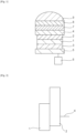
- Fig. 1 is a schematic sectional view of an organic photoelectric conversion element according to an embodiment of the present invention.
- the organic photoelectric conversion element includes a first organic compound layer 1 between a cathode 4 and an anode 5.
- the first organic compound layer 1 acts as a photoelectric conversion portion that converts light into charges. Since the first organic compound layer is intended to convert light into charges, it may be called a photoelectric conversion layer.
- the organic photoelectric conversion element further includes a second organic compound layer 2 between the first organic compound layer and the cathode, and a third organic compound layer 3 between the first organic compound layer and the anode.
- the anode 5 is connected to a readout circuit 6.
- the readout circuit 6 reads information according to the charge generated from the organic conversion portion and transmits the information to, for example, a signal processing section (not shown) disposed at the downstream side.
- the readout circuit 6 may be connected to the cathode.
- the organic photoelectric conversion element also includes an inorganic protective layer 7 over the cathode.
- the inorganic protective layer is made of, for example, silicon oxide, silicon nitride, aluminum oxide, or the like.
- the protective layer may be formed by vapor deposition, sputtering, ALD (atomic layer deposition), or the like.
- a color filter 8 is disposed on the inorganic protective layer.
- the color filter may transmit red light of visible light. If a plurality of organic photoelectric conversion elements are arranged, a plurality of color filters may be provided, one for each organic photoelectric conversion element. Alternatively, a single color filter may be shared by the plurality of organic photoelectric conversion elements.
- the color filters may be arranged for example, in a Bayer array.
- a microlens 9 is disposed on the color filter.
- the microlens focuses incoming light on the organic photoelectric conversion element. If a plurality of organic photoelectric conversion elements are arranged, a plurality of microlenses may be provided, one for each organic photoelectric conversion element. Alternatively, a single microlens may be shared by the plurality of organic photoelectric conversion elements.
- the voltage is desirably in the range of 0.5 V to 15 V.
- Fig. 2 is an energy diagram of an organic photoelectric conversion element according to an embodiment of the present invention.
- Fig. 2 shows only the cathode 4, the first organic compound layer 1, and the second organic compound layer 2, omitting other members or components.
- the line denoted by reference numeral 4 represents the energy level of the work function of the cathode.
- the length in the vertical direction represents the band gap of the organic compound contained in the corresponding organic compound layer; the position of the lower side of the rectangular shape represents the ionization potential of the organic compound; and the position of the upper side of the rectangular shape represents the electron affinity.
- any of the organic compound layers contains a plurality of organic compounds, the energy of the organic compound contained with the highest proportion is shown.
- the organic compound of the second organic compound layer has a lower ionization potential than the organic compound of the first organic compound layer. In this condition, holes can efficiently move from the first organic compound layer to the cathode.
- the ionization potential of the organic compound in the second organic compound layer is desirably 0.5 eV or more lower than that in the first organic compound layer. Also, the ionization potential of the organic compound in the second organic compound layer is desirably higher than the work function of the cathode.
- the ionization potential of the organic compound in the second organic compound layer be higher than the work function of the cathode and lower than the ionization potential of the organic compound in the first organic compound layer.
- the organic compound in the second organic compound layer has a lower electron affinity than the organic compound in the first organic compound layer. In this condition, electrons can be prevented from flowing into the first organic compound layer from the cathode. More specifically, the electron affinity of the organic compound in the second organic compound layer is desirably 0.5 eV or more lower than that in the first organic compound layer. Also, the electron affinity of the organic compound in the second organic compound layer is desirably 1.0 eV or more lower than the work function of the cathode.
- the organic compound in the second organic compound layer is resistant to water. This is because the second organic compound layer is disposed closer to the outside than the first organic compound layer, accordingly, more liable to be affected by moisture entering from the outside. More specifically, it is desirable that the organic compound in the second organic compound layer be less soluble in water or less reactive to water.
- the organic compound in the second organic compound layer is more resistant to water than the organic compound contained in the hole blocking layer disclosed in PTL 1.
- the water resistance of organic compounds can be estimated in accordance with the following procedure.
- An organic compound layer is formed to a thickness of 50 nm or more on a silicon substrate by vacuum deposition using resistance heating at 5 ⁇ 10 -3 Pa in a vacuum chamber of a vapor deposition apparatus. Water is dropped onto the organic compound layer and is allowed to stand for 10 minutes.
- the thickness of the organic compound layer is measured 10 minutes after water has been dropped.
- the water resistance thus can be estimated by comparing the thicknesses before and after dropping water.
- the rate of decrease in thickness at this time can be measured with, for example, an instrument P-16 manufactured by KLA-Tencor. This is calculated using the average of measurements at two points at both ends of a droplet trace.
- the rate of decrease in thickness of the water-resistant organic compound layer is desirably in the range of 0% to 50%, more desirably in the range of 0% to 30%, such as in the range of 0% to 10%.
- the water resistance may be estimated by measuring the contact angle of the water droplet with the organic compound layer, instead of measuring the rate of decrease in thickness.
- the contact angle can be measured by a known method.
- the contact angle may be measured with, for example, a contact angle meter DropMaster 700 and an analysis software program FAMAS (each manufactured by Kyowa Interface Science).
- the contact angle with the water-resistant organic compound layer is desirably in the range of 50° to 120°, such as in the range of 70° to 100°.
- a high water resistance of an organic compound layer suggests that the organic compound in the organic compound layer is resistant to water.
- Water-resistant organic compound layers are unlikely to be altered in surface profile of the organic compound layer even if water is dropped thereon. Therefore the contact angle of the water droplet is large or the rate of decrease in thickness is low.
- the second organic compound layer contains at least one selected from the group consisting of imidazolidene derivatives, benzoimidazolidene derivatives, and acridinylidene derivatives according to general formulas (1) - (6), as detailed in claim 1.
- the second organic compound layer may be in contact with the cathode.
- the ionization potential can be measured in accordance with the following procedure.
- An organic compound layer is formed on an Al/Nd substrate by vacuum deposition using resistance heating at 5 ⁇ 10 -3 Pa in a vacuum chamber. Desirably, the layer is deposited to a thickness in the range of about 150 nm to 200 nm. Then, the ionization potential of the resulting layer is measured with an atmospheric photoelectron spectrometer, for example, AC-2 manufactured by Riken Keiki.
- an atmospheric photoelectron spectrometer for example, AC-2 manufactured by Riken Keiki.
- the band gap can be measured in accordance with the following procedure.
- An organic compound layer is formed on an Al/Nd substrate by vacuum deposition using resistance heating at 5 ⁇ 10 -3 Pa in a vacuum chamber. Desirably, the layer is deposited to a thickness in the range of about 150 nm to 200 nm.
- an absorption spectrum is measured with an ultraviolet-visible spectrophotometer or the like. The band gap is determined from the absorption edge of the absorption spectrum.
- the ultraviolet-visible spectrophotometer may be, for example, V-560 manufactured by JASCO Corporation.
- the first organic compound layer of the organic photoelectric conversion element is intended to receive light and generate charges according to the amount of the light.
- the first organic compound layer may be called a photoelectric conversion layer because of the function thereof.
- the first organic compound layer may contain a plurality of organic compounds.
- the first organic compound layer contains a plurality of organic compounds
- a mixture of the plurality of organic compounds may form a single layer, or the plurality of organic compounds may form a multilayer composition including a plurality of layers.
- the plurality of organic compounds form a multilayer composite, it is desirable to form the layers of the composite in the direction from the anode to the cathode.
- the first organic compound layer contains a p-type organic semiconductor or an n-type organic semiconductor. More advantageously, the first organic compound layer has, at least in part, a bulk hetero layer (mixed layer) containing a mixture of a p-type organic compound and an n-type organic compound.
- the bulk hetero layer of the first organic compound layer can increase the photoelectric conversion efficiency (sensitivity) of the photoelectric conversion element.
- the bulk hetero layer contains organic compounds with an optimum proportion, the mobilities of electrons and holes in the first organic compound layer are increased, and accordingly the optical response speed of the organic photoelectric conversion element can be increased.
- the first organic compound layer contains fullerene or a fullerene derivative as the n-type organic semiconductor.
- a chain of molecules of the fullerene or fullerene derivative in the first organic compound layer defines a path of electrons and thus increases electron transportability, consequently increasing the optical response speed of the organic photoelectric conversion element.
- the fullerene or fullerene derivative content is desirably in the range of 40% by volume to 85% by volume relative to the total volume of the materials of the photoelectric conversion layer or the first organic compound layer.
- fullerenes or fullerene derivatives include Fullerene C60, Fullerene C70, Fullerene C76, Fullerene C78, Fullerene C80, Fullerene C82, Fullerene C84, Fullerene C90, Fullerene C96, Fullerene C240, Fullerene 540, mixed fullerenes, and fullerene nanotubes.
- the fullerene derivative is a fullerene having a substituent.
- the substituent may be an alkyl group, an aryl group, a heterocyclic group, or the like.
- the p-type organic semiconductor that may be contained in the first organic compound layer can act as an organic semiconductor donor, and is typically a hole-transporting, electron-donating organic compound. More specifically, the p-type organic semiconductor is one of the two organic compounds, having a lower ionization potential than the other.
- Examples of the p-type organic semiconductor that can be used in the first organic compound layer include triarylamine compounds, pyran compounds, quinacridone compounds, benzidine compounds, pyrazoline compounds, styrylamine compounds, hydrazone compounds, triphenylmethane compounds, carbazole compounds, polysilane compounds, thiophene compounds, phthalocyanine compounds, cyanine compounds, merocyanine compounds, oxonol compounds, polyamine compounds, indole compounds, pyrrole compounds, pyrazole compounds, polyarylene compounds, condensed aromatic hydrocarbons (naphthalene derivatives, anthracene derivatives, phenanthrene derivatives, tetracene derivatives, pyrene derivatives, perylene derivatives, fluoranthene derivatives), and metal complexes having nitrogen-containing heterocyclic compounds as ligands.
- triarylamine compounds pyran compounds, quinacridone compounds, pyrrole compounds, phthalo
- Fluoranthene derivatives are compounds having a fluoranthene skeleton in the chemical structure thereof.
- naphthalene derivatives, anthracene derivatives, phenanthrene derivatives, tetracene derivatives, pyrene derivatives, and perylene derivatives are each a compound having the skeleton of the corresponding chemical compound in the chemical structure thereof.
- the first organic compound layer is not luminescent. More specifically, “not luminescent” implies that the layer has a luminescent quantum efficiency of 1% or less, desirably 0.5% or less, such as 0.1% or less, in the visible wavelength region (400 nm to 730 nm). If the luminescent quantum efficiency of the photoelectric conversion portion exceeds 1%, sensing performance or imaging performance is adversely affected when the organic photoelectric conversion element is applied to a censor or an imaging device.
- the organic photoelectric conversion element according to an embodiment of the present invention may further include a third organic compound layer between the anode and the first organic compound layer.
- the third organic compound layer is intended to prevent holes from entering the first organic compound layer from the anode and desirably has a high ionization potential.
- the organic compound layer according to an embodiment may include a substrate.
- the substrate may be a silicon substrate, a glass substrate, a flexible substrate, or the like.
- the cathode of the organic photoelectric conversion element is an electrode that collects holes of the charges generated in the photoelectric conversion portion.
- the cathode may be made of an electrically conductive transparent material. In a structure where the cathode is disposed near the side of the organic photoelectric conversion element through which light enters, it is desirable that the cathode be optically transparent.
- the cathode may be called a hole-collecting electrode or a negative electrode.
- cathode material examples include metals, metal oxides, metal nitrides, metal borides, organic electroconductive compounds, and mixture thereof. More specifically, cathode materials include elemental metals, such as gold, platinum, silver, copper, nickel, palladium, cobalt, selenium, vanadium, tungsten, aluminum, titanium, and manganese; mixtures or alloys of these elemental metals; antimony- or fluorine-doped tin oxide (ATO, FTO); electroconductive metal oxides, such as tin oxide, zinc oxide, indium oxide, indium tin oxide (ITO), and indium zinc oxide (IZO); inorganic electroconductive compounds, such as copper iodide and copper sulfide; organic electroconductive materials, such as polyaniline, polythiophene, and polypyrrole; and composites including an organic electroconductive material layer and an ITO or titanium nitride layer.
- elemental metals such as gold, platinum, silver, copper, nickel, palladium,
- the anode of the organic photoelectric conversion element is an electrode that collects electrons of the charges generated in the photoelectric conversion portion.
- the anode In a structure where the anode is disposed on the side of the organic photoelectric conversion element through which light enters, it is desirable that the anode be optically transparent.
- the anode may be called an electron-collecting electrode or a positive electrode.
- cathode material examples include metals, metal oxides, metal nitrides, metal borides, organic electroconductive compounds, and mixture thereof. More specifically, cathode materials include elemental metals, such as gold, platinum, silver, copper, nickel, palladium, cobalt, selenium, vanadium, tungsten, aluminum, titanium, and manganese; mixtures or alloys of these elemental metals; antimony- or fluorine-doped tin oxide (ATO, FTO); electroconductive metal oxides, such as tin oxide, zinc oxide, indium oxide, Al-doped zinc oxide (AZO), indium tin oxide (ITO), indium zinc oxide (IZO), and TiO 2 ; inorganic electroconductive compounds, such as copper iodide and copper sulfide; organic electroconductive materials, such as polyaniline, polythiophene, and polypyrrole; and composites including an organic electroconductive material layer and an ITO or titanium nitride layer.
- elemental metals
- One of the anode and the cathode that is connected to the readout circuit may be called the pixel electrode.
- the anode and the cathode may be called the pixel electrode and the opposing electrode, respectively.
- the ITO electrode can be formed by an electron beam method, sputtering, resistance heating vapor deposition, a chemical reaction method (for example, sol-gel method), coating with an indium tin oxide dispersion, and so forth.
- the resulting ITO electrode may be subjected to UV-ozone treatment, plasma treatment, or the like.
- the TiN electrode can be formed by reactive sputtering or any other method, and the resulting TiN electrode may be subjected to annealing, UV-ozone treatment, plasma treatment, or the like.
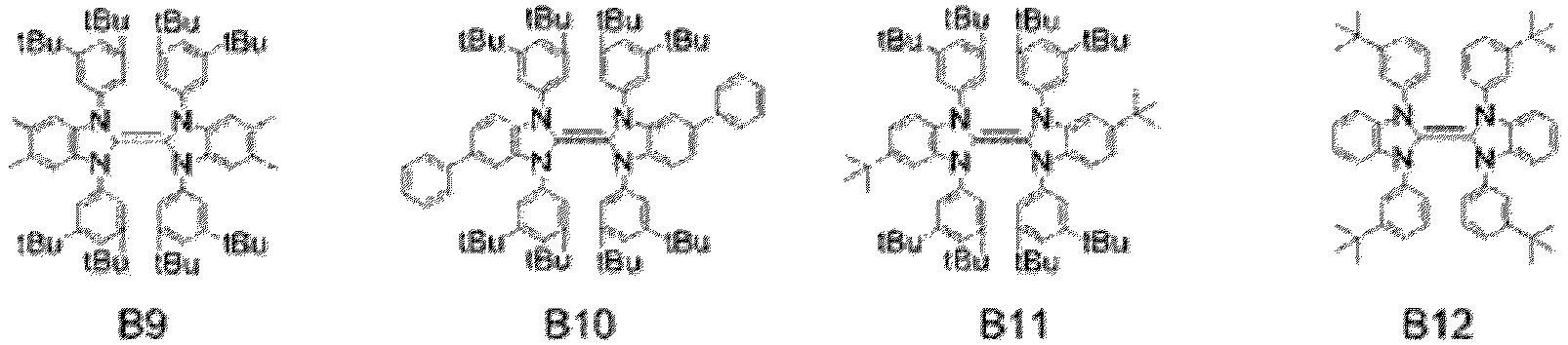
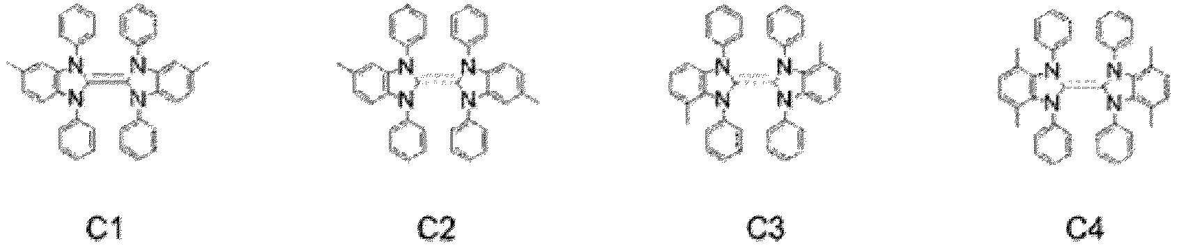
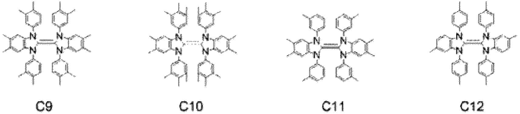
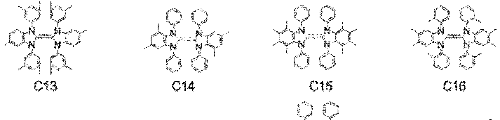
- the organic compound in the second organic compound layer (2) represented by the general formula (1) is one of the following organic compounds:
- the organic compound in the second organic compound layer (2) represented by the general formula (2) is one of the following organic compounds:
- the organic compound in the second organic compound layer (2) represented by the general formula (3) is one of the following organic compounds:
- the organic compound in the second organic compound layer (2) represented by the general formula (4) is one of the following organic compounds:
- the organic compound in the second organic compound layer (2) represented by the general formula (5) is one of the following organic compounds:
- the organic compound in the second organic compound layer (2) represented by the general formula (6) is one of the following organic compounds:
- a process for synthesizing an organic compound of general formula (1) is disclosed by David M. Lemal in “Journal of American Chemical Society, 1964, 86 (12), pp 2518-2519 ".
- a variety of organic compounds represented by general formula (1) can be synthesized by appropriately replacing the reagent used in the disclosed process.
- a process for synthesizing an organic compound of general formula (2) is disclosed by H. W. Wanzlick in "Organic Syntheses, Coll. Vol. 5, p. 115 (1973 ) and Vol. 47, p. 14 (1967 )".
- a variety of organic compounds represented by general formula (2) can be synthesized by appropriately replacing the reagents used in the disclosed process.
- An organic compound of general formula (3) may be synthesized by, for example, the following process.
- a variety of organic compounds represented by general formula (3) can be synthesized by appropriately replacing the reagents corresponding to R 1 to R 4 , X 1 and X 2 .
- Exemplified Compound A-1 of general formula (3) was synthesized by the following scheme.
- An organic compound of general formula (4) may be synthesized by, for example, the following scheme.
- a variety of organic compounds represented by general formula (4) can be synthesized by appropriately replacing the reagents corresponding to R 1 and R 2 .
- Exemplified Compound A1 of general formula (4) was synthesized by the following scheme.
- the resulting compound was subjected to matrix-assisted laser desorption/ionization time-of-flight mass spectrometry (MALDI-TOF-MS) using Autoflex LRF manufactured by Bruker.
- MALDI-TOF-MS matrix-assisted laser desorption/ionization time-of-flight mass spectrometry
- CV measurement was performed in 0.1 M solution of tetrabutylammonium perchlorate in N,N-dimethylformamide with a Ag/Ag + reference electrode, a Pt counter electrode, and a glassy carbon working electrode.
- the potential scan rate was 0.5 V/s.
- Oxidation potential was -0.85 V.
- An organic compound of general formula (5) may be synthesized by, for example, the following process.
- a variety of organic compounds represented by general formula (5) can be synthesized by appropriately replacing the reagents corresponding to R 1 and R 2 .
- CV measurement was performed in 0.1 M solution of tetrabutylammonium perchlorate in N,N-dimethylformamide with a Ag/Ag + reference electrode, a Pt counter electrode, and a glassy carbon working electrode.
- the potential scan rate was 0.5 V/s.
- Oxidation potential was -0.98 V.
- a variety of organic compounds represented by general formula (6) can be synthesized by appropriately replacing the reagents corresponding to R 1 and R 2 .
- Exemplified Compound A2 of general formula (6) was synthesized by the following scheme.
- CV measurement was performed in 0.1 M solution of tetrabutylammonium perchlorate in N,N-dimethylformamide with a Ag/Ag + reference electrode, a Pt counter electrode, and a glassy carbon working electrode.
- the potential scan rate was 0.5 V/s.
- Oxidation potential was -0.74V.
- an organic photoelectric conversion element for light having a different color By replacing the organic compound used in the first organic compound layer, another organic photoelectric conversion element for light having a different color can be produced.
- An organic photoelectric conversion element for light having a different color implies that the element converts light in a different wavelength range from the light to be photoelectrically converted by other photoelectric conversion elements.
- the organic photoelectric conversion element of an embodiment of the present invention may be used in an optical area sensor.
- the optical area sensor includes a plurality of organic photoelectric conversion elements arranged in a two-dimensional array defined by rows and columns.
- the organic photoelectric conversion elements each generate charges and independently output the charges, and thus the optical area sensor provides information representing the distribution of light intensity in a specific light-receiving area.
- Each of the plurality of organic photoelectric conversion elements of the optical area sensor may be provided with an additional optical photoelectric conversion element capable of converting light having a different color into electric energy.
- the additional organic photoelectric conversion element is disposed on the other organic photoelectric conversion element.
- the additional organic photoelectric conversion element photoelectrically converts light having a wavelength different from the light to be converted by the other organic photoelectric conversion element.
- the organic photoelectric conversion element of an embodiment of the present invention may be used in an imaging device.
- the imaging device includes a plurality of pixels and a signal processing section.
- the plurality of pixels are arranged in a matrix manner including a plurality of rows and a plurality of columns.
- Each pixel in this structure outputs a signal to provide an image signal.
- each pixel includes at least one organic photoelectric conversion element.
- the pixel may include a readout circuit connected to the organic photoelectric conversion element.
- the readout circuit includes a transistor that outputs, for example, signals according to the charge generated in the organic photoelectric conversion element.
- the pixel may further include an additional organic photoelectric conversion element capable of photoelectrically converting light having a different color from the light to be converted by the other organic photoelectric conversion element.
- the additional organic photoelectric conversion element is disposed on the other organic photoelectric conversion element.
- the additional organic photoelectric conversion element photoelectrically converts light having a wavelength different from the light to be converted by the other organic photoelectric conversion element.
- the pixel may include a plurality of organic photoelectric conversion elements. Such a structure enables phase difference auto-focusing on an imaging surface. Two or more of the plurality of pixels may share a readout circuit.
- the imaging device may include a wavelength selecting section.
- the wavelength selecting section may be a color filter.
- the color filter is disposed near the side through which light enters.
- a specific color refers to light in a range of specific wavelengths.
- a plurality of color filters may be provided, one for each pixel, or a single color filter may be shared by the plurality of pixels.
- the wavelength selecting section may be a prism that separates out light having a specific wavelength.
- the imaging device may include a microlens.
- the microlens is disposed near the side through which light enters and is adapted to collect incoming light to a photoelectric conversion portion.
- a plurality of microlenses may be provided, one for each pixel, or a single microlens may be shared by the plurality of pixels.
- an optical filter may be disposed near the side of the imaging device through which light enters.
- the optical filter may be a low-pass filter, a UV-cut filter capable of removing light having wavelengths lower than or equal to the wavelengths of ultraviolet radiation, or an IR-cut filter capable of removing infrared radiation. Since the optical filter reduces noise, the imaging device can form high-quality images.
- the organic photoelectric conversion element of an embodiment of the present invention may be used in an imaging apparatus.
- An imaging apparatus includes an imaging optical system having a plurality of lenses, and an imaging device capable of receiving light that has passed through the imaging optical system.
- the imaging apparatus includes a joint section that can be connected to an imaging optical system, and an imaging device.
- the imaging apparatus may be a digital camera or a digital still camera.
- the imaging apparatus may further include a receiver adapted to receive a signal from the outside.
- the signal that the receiver receives is used for controlling at least the imaging range, imaging start point and imaging end point of the imaging apparatus.
- the imaging apparatus may further include a transmitter adapted to transmit an obtained image to the outside. The transmission is performed in a wired manner or a wireless manner.
- a known communication system may be used, such as Wi-Fi or Bluetooth (registered trademark).
- the presence of the receiver and the transmitter enables the imaging apparatus to be used as a network camera.
- a layer of the organic compound was formed on an Al/Nd substrate by vacuum deposition using resistance heating at 5 ⁇ 10 -3 Pa in a vacuum chamber.
- the organic compound layer was formed to a thickness of 150 nm to 200 nm.
- the ionization potential of the resulting layer was measured with an atmospheric photoelectron spectrometer (AC-2 manufactured by Riken Keiki).
- a layer of the organic compound was formed on an Al/Nd substrate by vacuum deposition using resistance heating at 5 ⁇ 10 -3 Pa in a vacuum chamber.
- the organic compound layer was formed to a thickness of 150 nm to 200 nm.
- the absorption spectrum of the organic compound layer was measured with an ultraviolet-visible spectrophotometer (V-560 manufactured by JASCO Corporation). The band gap was determined from the absorption edge of the absorption spectrum.
- a 50 nm-thick organic compound layer was formed of Exemplified Compound A3 on a silicon substrate by vapor deposition.
- an organic photoelectric conversion element in which holes generated by photoelectric conversion can efficiently move to the cathode.
Landscapes
- Physics & Mathematics (AREA)
- Chemical & Material Sciences (AREA)
- Engineering & Computer Science (AREA)
- Materials Engineering (AREA)
- Spectroscopy & Molecular Physics (AREA)
- Electromagnetism (AREA)
- Inorganic Chemistry (AREA)
- Light Receiving Elements (AREA)
- Solid State Image Pick-Up Elements (AREA)
- Studio Devices (AREA)
- Electroluminescent Light Sources (AREA)
- Transforming Light Signals Into Electric Signals (AREA)
Claims (19)
- Organisches fotoelektrisches Umwandlungselement, das aufweist:eine Anode (5);eine Kathode (4);einen fotoelektrischen Umwandlungsanteil, der zwischen der Anode (5) und der Kathode (4) angeordnet ist, wobei der fotoelektrische Umwandlungsanteil eine erste organische Verbindungsschicht (1), die eine organische Verbindung enthält, enthält; undeine zweite organische Verbindungsschicht (2), die zwischen der Kathode (4) und dem fotoelektrischen Umwandlungsanteil angeordnet ist, wobei die zweite organische Verbindungsschicht (2) eine organische Verbindung enthält und die zweite organische Verbindungsschicht (2) zumindest eines, das aus einer Gruppe, die aus Imidazolidenableitungen, Benzoimidazolidenableitungen und Acridinylidenableitungen besteht, ausgewählt ist, enthält,die organische Verbindung in der zweiten organischen Verbindungsschicht (2) durch eine der allgemeinen Formeln (1) bis (6) repräsentiert ist:
 wobei in Formel (1), R1 bis R4 jeweils eine Gruppe, die aus den Gruppen, die aus substituierten oder nicht-substituierten Phenylgruppen, substituierten oder nicht-substituierten Benzylgruppen, substituierten oder nicht-substituierten Biphenylgruppen, substituierten oder nicht-substituierten Naphthylgruppen, substituierten oder nicht-substituierten Phenantrenylgruppen, substituierten oder nicht-substituierten Flourenylgruppen, substituierten oder nicht-substituierten Triphenylenylgruppen, substituierten oder nicht-substituierten Dibenzofuranylgruppen, und substituierten oder nicht-substituierten Dibenzothiophenylgruppen besteht, ausgewählt ist, repräsentieren;R5 bis R12 jeweils ein Wasserstoffatom oder eine Gruppe, die aus der Gruppe, die aus Alkylgruppen, die eine Kohlenstoffanzahl in dem Bereich von 1 bis 4 haben, und substituierten oder nicht-substituierten Arylgruppen besteht, ausgewählt ist, repräsentieren;die Arylgruppe eine Alkylgruppe mit einer Kohlenstoffanzahl in dem Bereich von 1 bis 4 als ein Substituent haben kann,wobei die organische Verbindung in der zweiten organischen Verbindungsschicht (2), die durch die allgemeine Formel (1) repräsentiert wird, eine der folgenden organischen Verbindungen ist:


 wobei in Formel (2), R1 bis R4 jeweils eine Gruppe, die aus den Gruppen, die aus substituierten oder nicht-substituierten Phenylgruppen, substituierten oder nicht-substituierten Biphenylgruppen, substituierten oder nicht-substituierten Naphthylgruppen, substituierten oder nicht-substituierten Phenantrengruppen, substituierten oder nicht-substituierten Fluorenylgruppen, substituierten oder nicht-substituierten Triphenylengruppen, substituierten oder nicht-substituierten Dibenzofurangruppen, und substituierten oder nicht-substituierten Dibenzothiophengruppen bestehen, repräsentieren;wobei die organische Verbindung in der zweiten organischen Verbindungsschicht (2), die durch die allgemeine Formel (2) repräsentiert wird, eine der folgenden organischen Verbindungen ist:


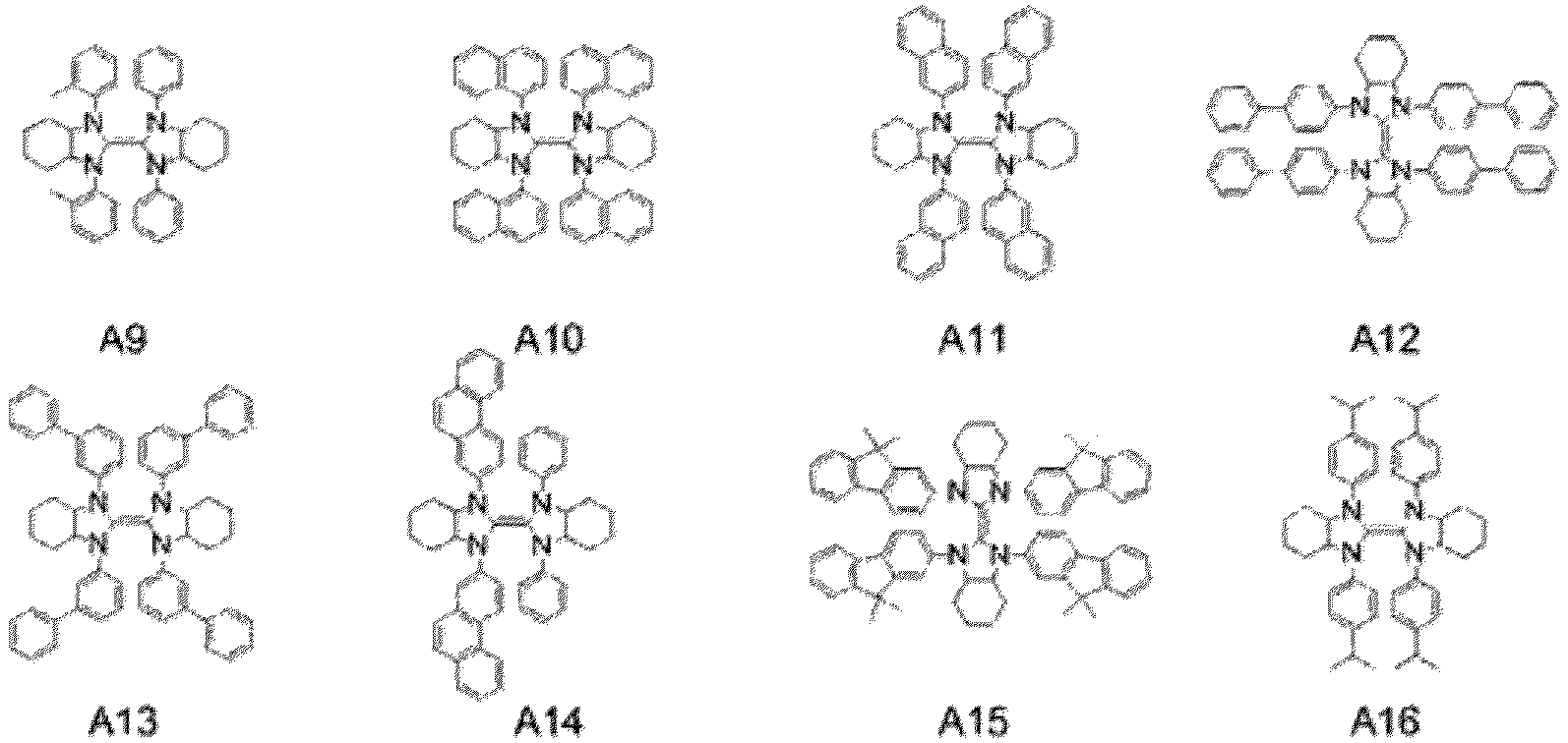

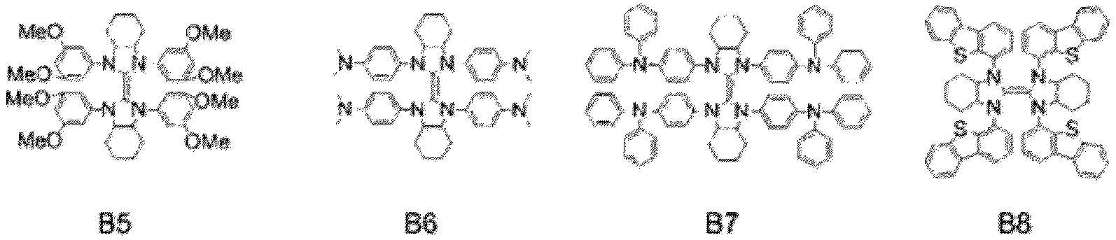
 wobei in Formel (3), X1 und X2 jeweils eine Arylgruppe repräsentieren;die Arylgruppe ein Halogenatom oder eine Alkylgruppe aufweisen kann, R1 bis R16 jeweils ein Wasserstoffatom oder einen Substituenten, der aus der Gruppe, die aus Halogenatomen, Alkylgruppen, und Arylgruppen besteht, ausgewählt ist, repräsentieren,wobei die organische Verbindung in der zweiten organischen Verbindungsschicht (2), die durch die allgemeine Formel (3) repräsentiert wird, eine der folgenden organischen Verbindungen ist:

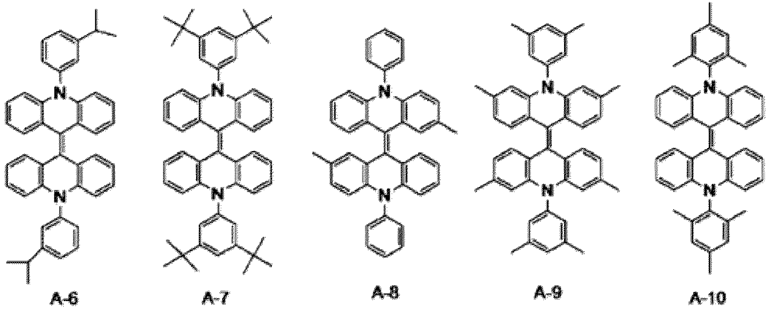

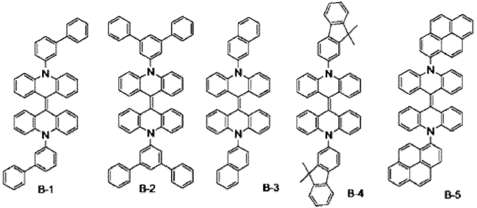


 wobei in Formel (4), R1 bis R28 jeweils ein Wasserstoffatom oder einen Substituenten, der aus der Gruppe, die aus Halogenatomen, Alkylgruppen, die eine Kohlenstoffanzahl in dem Bereich von 1 bis 8 haben, und substituierten oder nicht-substituierten Arylgruppen besteht, ausgewählt ist, repräsentieren,wobei die organische Verbindung in der zweiten organischen Verbindungsschicht (2), die durch die allgemeine Formel (4) repräsentiert wird, eine der folgenden organischen Verbindungen ist:


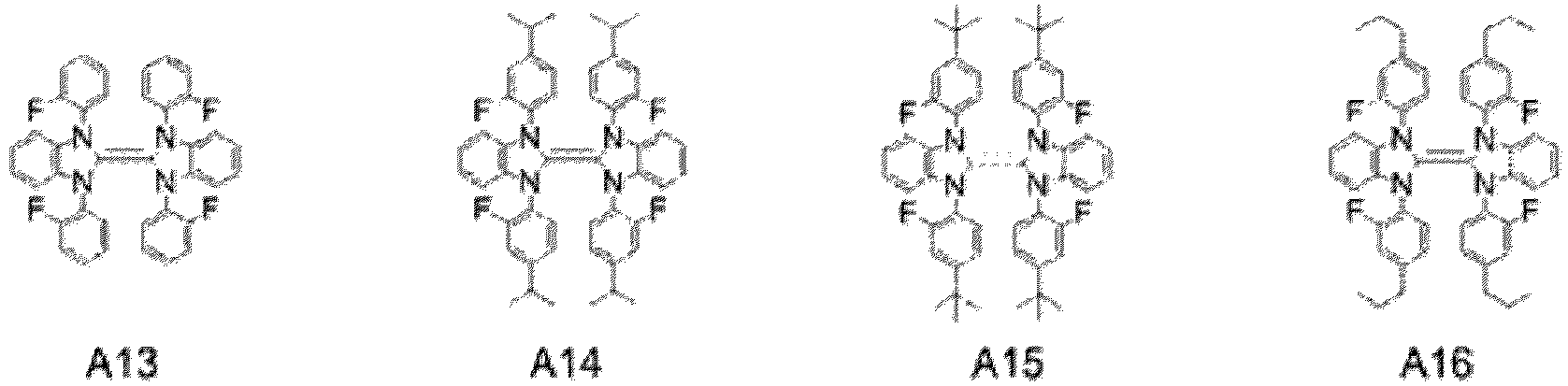




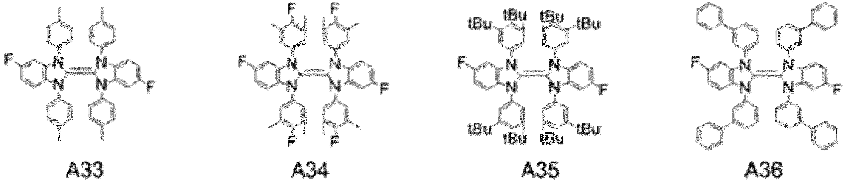
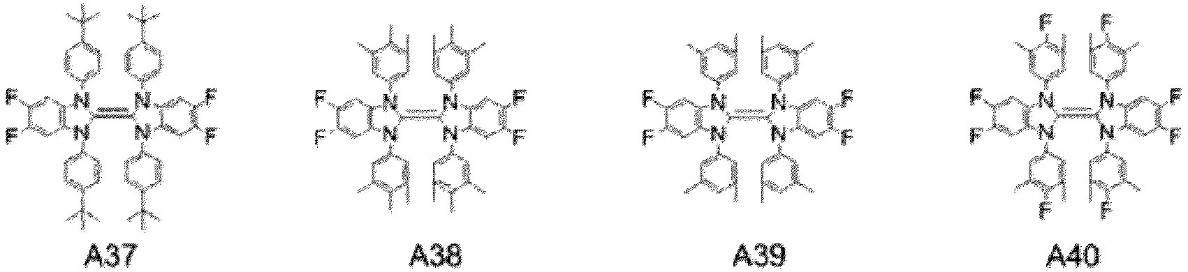







 wobei in Formel (5) Ar1 bis Ar4 jeweils einen substituierten oder nicht-substituierten kondensierten Ring repräsentieren;R1 bis R8 jeweils ein Wasserstoffatom oder einen Substituenten, der aus der Gruppe, die aus Halogenatomen, Alkylgruppen, die eine Kohlenstoffanzahl in dem Bereich von 1 bis 8 haben, und substituierten oder nicht-substituierten Arylgruppen besteht, ausgewählt ist, repräsentieren,wobei die organische Verbindung in der zweiten organischen Verbindungsschicht (2), die durch die allgemeine Formel (5) repräsentiert wird, eine der folgenden organischen Verbindungen ist:


 wobei in der allgemeinen Formel (6), Ar1 bis Ar4 jeweils eine substituierte oder nicht-substituierte heteromonozyklische Gruppe repräsentieren;R1 bis R8 jeweils ein Wasserstoffatom oder einen Substituenten, der aus der Gruppe, die aus Halogenatomen, Alkylgruppen, die eine Kohlenstoffanzahl in dem Bereich von 1 bis 8 haben, und substituierten oder nicht-substituierten Arylgruppen besteht, ausgewählt ist, repräsentieren,wobei die organische Verbindung in der zweiten organischen Verbindungsschicht (2), die durch die allgemeine Formel (6) repräsentiert wird, eine der folgenden organischen Verbindungen ist:


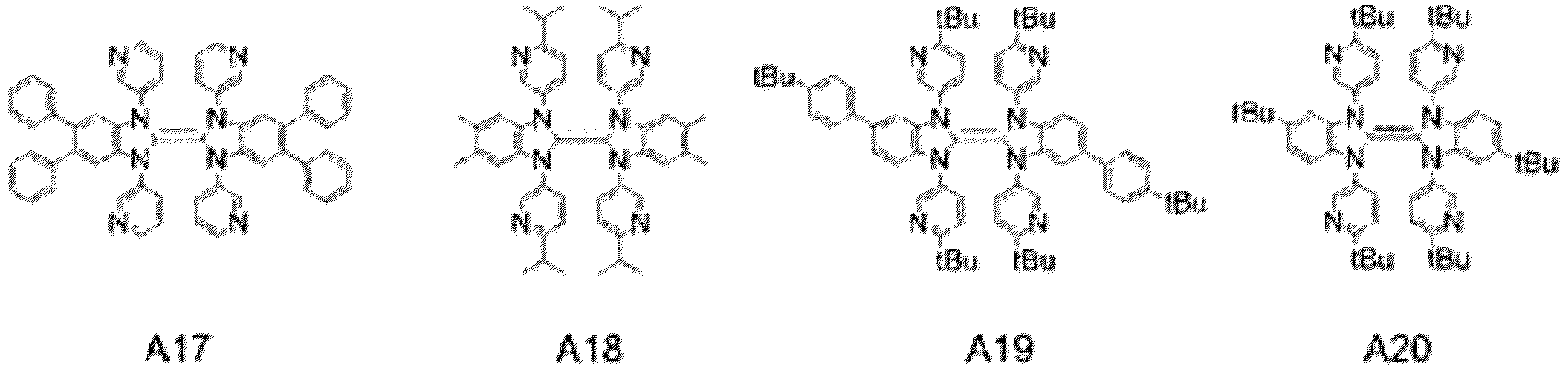

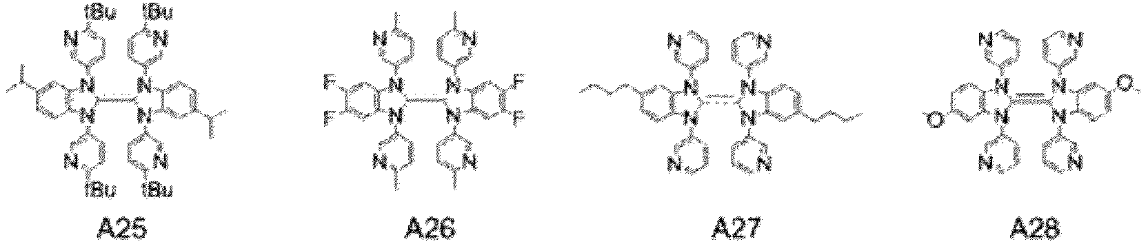


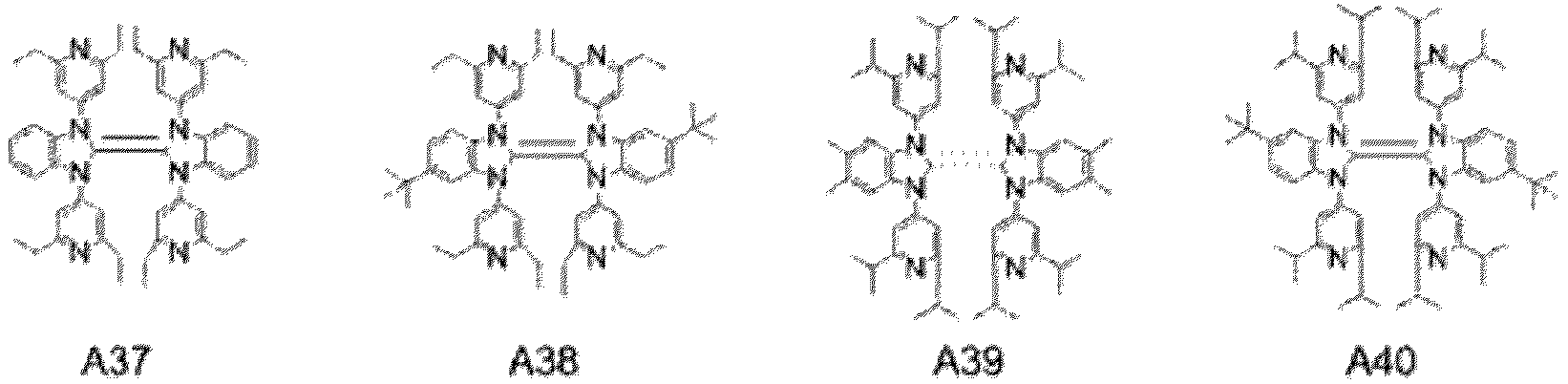
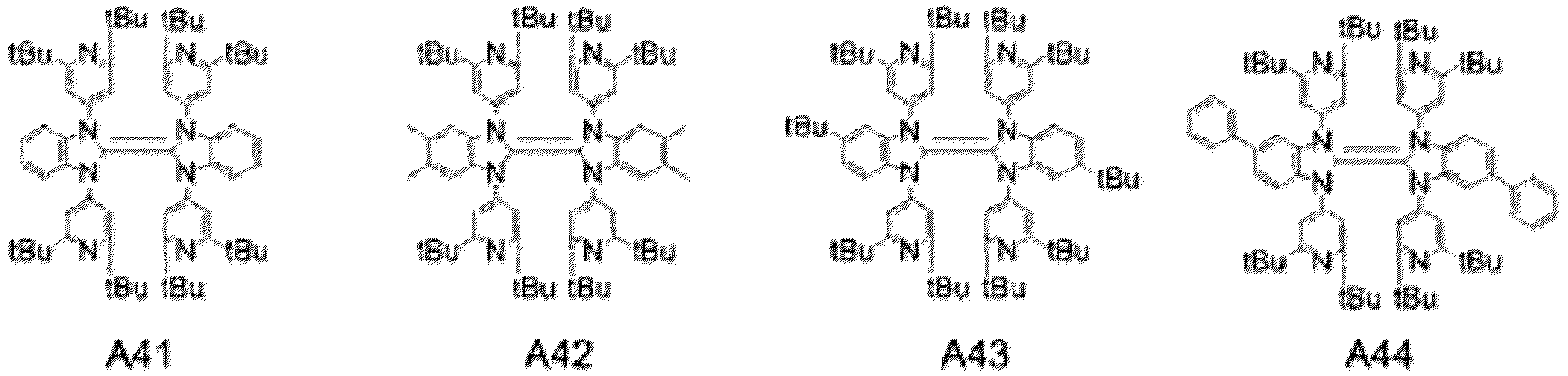
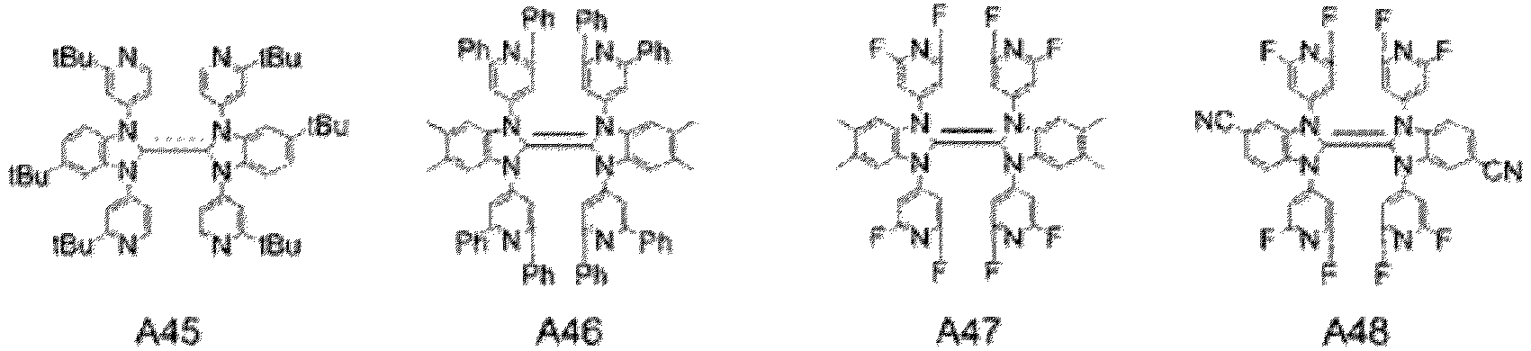


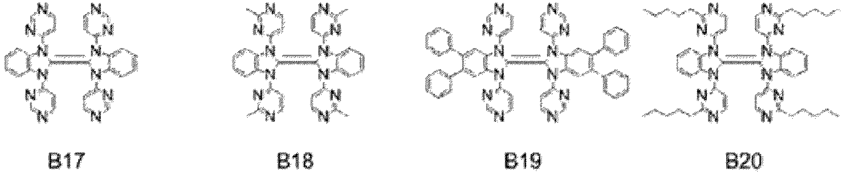


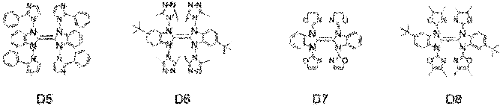
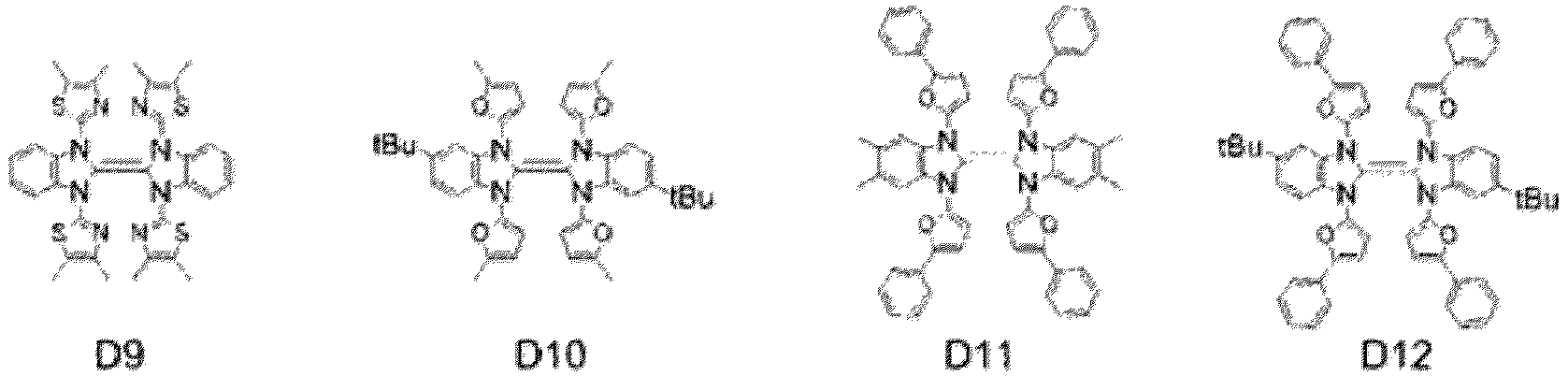


- Organisches fotoelektrisches Umwandlungselement nach Anspruch 1, wobei die Elektronenaffinität der organischen Verbindung in der zweiten organischen Verbindungsschicht (2) um 0,5 eV oder mehr niedriger als die Elektronenaffinität der organischen Verbindung in der ersten organischen Verbindungsschicht (1) ist.
- Organisches fotoelektrisches Umwandlungselement nach Anspruch 1 oder 2, wobei die Elektronenaffinität der organischen Verbindung in der zweiten organischen Verbindungsschicht (2) um 1,0 eV oder mehr niedriger als die Arbeitsfunktion der Kathode (4) ist.
- Organisches fotoelektrisches Umwandlungselement nach einem der Ansprüche 1 bis 3, wobei ein Ionisationspotenzial der organischen Verbindung in der zweiten organischen Verbindungsschicht (2) niedriger als das der organischen Verbindung in der ersten organischen Verbindungsschicht (1) ist.
- Organisches fotoelektrisches Umwandlungselement nach Anspruch 4, wobei das Ionisationspotenzial der organischen Verbindung in der zweiten organischen Verbindungsschicht (2) um 0,5 eV oder mehr niedriger als das Ionisationspotenzial der organischen Verbindung in der ersten organischen Verbindungsschicht (1) ist.
- Organisches fotoelektrisches Umwandlungselement nach einem der Ansprüche 1 bis 5, wobei die erste organische Verbindungsschicht (1) eine Vielzahl von organischen Verbindungen enthält.
- Organisches fotoelektrisches Umwandlungselement nach einem der Ansprüche 1 bis 6, wobei der fotoelektrische Umwandlungsanteil ferner eine dritte organische Verbindungsschicht (3) enthält, die zwischen der ersten organischen Verbindungsschicht (1) und der Anode (5) angeordnet ist, wobei die dritte organische Verbindungsschicht (3) in Kontakt mit der ersten organischen Verbindungsschicht (1) ist.
- Organisches fotoelektrisches Umwandlungselement nach einem der Ansprüche 1 bis 7, wobei die zweite organische Verbindungsschicht (2) in Kontakt mit der Kathode (4) ist.
- Optischer Flächensensor, der eine Vielzhal von organischen fotoelektrischen Umwandlungselementen nach einem der Ansprüche 1 bis 8 aufweist, wobei die organischen fotoelektrischen Umwandlungselemente in einer zweidimensionalen Anordnung einschließlich einer Vielzahl von Zeilen und einer Vielzahl von Spalten angeordnet sind.
- Optischer Flächensensor nach Anspruch 9, wobei jedes der Vielzahl der organischen fotoelektrischen Umwandlungselemente mit einem zusätzlichen organischen fotoelektrischen Umwandlungselement bereitgestellt ist, das in der Lage ist, fotoelektrisch ein Licht, das eine andere Farbe als das Licht, das durch das andere fotoelektrische Umwandlungselement umzuwandeln ist, umzuwandeln, und wobei jedes der organischen fotoelektrischen Umwandlungselemente und der entsprechenden zusätzlichen organischen fotoelektrischen Umwandlungselemente aufeinander angeordnet sind.
- Abbildungseinrichtung, die aufweist:eine Vielzahl von Pixeln, die in einer zweidimensionalen Anordnung einschließlich einer Vielzahl von Zeilen und einer Vielzahl von Spalten angebracht sind, undeinen Signalverarbeitungsabschnitt, der mit den Pixeln verbunden ist,wobei jeder der Pixel das organische fotoelektrische Umwandlungselement nach einem der Ansprüche 1 bis 8 und eine Ausleseschaltung, die mit dem organischen fotoelektrischen Umwandlungselement verbunden ist, aufweist.
- Abbildungseinrichtung nach Anspruch 11, wobei jeder der Pixel ferner ein zusätzliches organisches fotoelektrisches Umwandlungselement, das in der Lage ist, fotoelektrisch ein Licht, das eine von dem Licht, das durch das andere organische fotoelektrische Umwandlungselement umzuwandeln ist, verschieden ist, fotoelektrisch umzuwandeln, wobei die organischen fotoelektrischen Umwandlungselemente von jedem Pixel aufeinander angeordnet sind.
- Abbildungseinrichtung nach Anspruch 12, die ferner zumindest ein Bauteil, das aus der Gruppe, die aus einem Wellenlängenauswahlabschnitt, einer Mikrolinse und einem optischen Filter besteht, nahe an einer Seite, durch die Licht einfällt, aufweist.
- Abbildungseinrichtung nach Anspruch 13, wobei zumindest ein Bauteil für jedes der Vielzahl von Pixeln bereitgestellt ist.
- Abbildungsvorrichtung, die aufweist:ein optisches Abbildungssystem; undeine Abbildungseinrichtung nach einem der Ansprüche 11 bis 14, wobei die Abbildungseinrichtung in der Lage ist, Licht, das durch das optische Abbildungssystem gegangen ist, zu empfangen.
- Abbildungsvorrichtung nach Anspruch 15, die ferner aufweist:
einen Verbindungsabschnitt, der in der Lage ist, mit einem optischen Abbildungssystem verbunden zu werden. - Abbildungsvorrichtung nach Anspruch 15 oder 16, wobei die Abbildungsvorrichtung eine Digitalkamera oder eine digitale Standbildkamera ist.
- Abbildungsvorrichtung nach einem der Ansprüche 15 bis 17, die ferner einen Empfänger, der angepasst ist, ein Signal von außerhalb zu empfangen, aufweist, wobei das Signal dafür verwendet wird, zumindest einen Abbildungsbereich davon, einen Abbildungsstartpunkt davon und einen Abbildungsendpunkt davon zu steuern.
- Abbildungsvorrichtung nach einem der Ansprüche 15 bis 18, ferner mit einem Transmitter, der angepasst ist, ein erhaltenes Bild nach außen zu übertragen.
Applications Claiming Priority (2)
| Application Number | Priority Date | Filing Date | Title |
|---|---|---|---|
| JP2015115237 | 2015-06-05 | ||
| PCT/JP2016/002520 WO2016194337A1 (en) | 2015-06-05 | 2016-05-24 | Organic photoelectric conversion element, optical area sensor, imaging device, and imaging apparatus |
Publications (3)
| Publication Number | Publication Date |
|---|---|
| EP3304599A1 EP3304599A1 (de) | 2018-04-11 |
| EP3304599A4 EP3304599A4 (de) | 2019-02-27 |
| EP3304599B1 true EP3304599B1 (de) | 2024-10-09 |
Family
ID=57440930
Family Applications (1)
| Application Number | Title | Priority Date | Filing Date |
|---|---|---|---|
| EP16802779.5A Active EP3304599B1 (de) | 2015-06-05 | 2016-05-24 | Organisches fotoelektrisches umwandlungselement, optischer flächensensor, bildgebungsvorrichtung und bildgebungsvorrichtung |
Country Status (5)
| Country | Link |
|---|---|
| US (1) | US10541260B2 (de) |
| EP (1) | EP3304599B1 (de) |
| JP (1) | JP6833351B2 (de) |
| CN (1) | CN107615489B (de) |
| WO (1) | WO2016194337A1 (de) |
Families Citing this family (9)
| Publication number | Priority date | Publication date | Assignee | Title |
|---|---|---|---|---|
| JP6552257B2 (ja) * | 2015-04-30 | 2019-07-31 | キヤノン株式会社 | 1位、1’位、3位、3’位に複素単環基を有する、2,2’−ビベンゾ[d]イミダゾリデン化合物、それを有する有機発光素子、表示装置 |
| US10271037B2 (en) * | 2017-01-20 | 2019-04-23 | Semiconductor Components Industries, Llc | Image sensors with hybrid three-dimensional imaging |
| JP6932564B2 (ja) * | 2017-06-23 | 2021-09-08 | キヤノン株式会社 | 有機光電変換素子、撮像素子及び撮像装置 |
| JP7346011B2 (ja) | 2017-09-20 | 2023-09-19 | キヤノン株式会社 | 有機化合物及び光電変換素子 |
| JP7046562B2 (ja) * | 2017-10-25 | 2022-04-04 | キヤノン株式会社 | 有機化合物及び光電変換素子 |
| WO2020090989A1 (ja) * | 2018-10-31 | 2020-05-07 | 日産化学株式会社 | フッ化芳香族第二級または第三級アミン化合物の製造方法 |
| EP3923361A4 (de) | 2019-02-08 | 2022-04-06 | Panasonic Intellectual Property Management Co., Ltd. | Element zur fotoelektrischen umwandlung und bildgebungsvorrichtung |
| CN111039924A (zh) * | 2019-11-26 | 2020-04-21 | 武汉华星光电半导体显示技术有限公司 | 以乙烯双吖啶为核的空穴传输材料及有机发光二极管 |
| CN115244063B (zh) * | 2020-01-08 | 2025-03-07 | 罗特格斯新泽西州立大学 | 过渡金属催化剂的配体 |
Family Cites Families (17)
| Publication number | Priority date | Publication date | Assignee | Title |
|---|---|---|---|---|
| JP2003303683A (ja) * | 2002-04-09 | 2003-10-24 | Semiconductor Energy Lab Co Ltd | 発光装置 |
| US20040118444A1 (en) * | 2002-12-20 | 2004-06-24 | General Electric Company | Large-area photovoltaic devices and methods of making same |
| JP4677314B2 (ja) * | 2005-09-20 | 2011-04-27 | 富士フイルム株式会社 | センサーおよび有機光電変換素子の駆動方法 |
| EP2000464A4 (de) | 2006-03-27 | 2010-06-30 | Idemitsu Kosan Co | Stickstoffhaltiges heterozyklisches derivat und organische elektrolumineszenzvorrichtung damit |
| JP2008072090A (ja) | 2006-08-14 | 2008-03-27 | Fujifilm Corp | 光電変換素子及び固体撮像素子 |
| FI20070063A0 (fi) * | 2007-01-24 | 2007-01-24 | Ronald Oesterbacka | Orgaaninen kenttävaikutustransistori |
| JP5376963B2 (ja) * | 2008-01-25 | 2013-12-25 | 富士フイルム株式会社 | 光電変換素子及び撮像素子 |
| JP2009200752A (ja) * | 2008-02-20 | 2009-09-03 | Panasonic Corp | カメラモジュール |
| US8664518B2 (en) * | 2009-12-11 | 2014-03-04 | Konica Minolta Holdngs, Inc. | Organic photoelectric conversion element and producing method of the same |
| JP5585232B2 (ja) * | 2010-06-18 | 2014-09-10 | ソニー株式会社 | 固体撮像装置、電子機器 |
| US9349964B2 (en) * | 2010-12-24 | 2016-05-24 | Lg Chem, Ltd. | Organic light emitting diode and manufacturing method thereof |
| JP6025243B2 (ja) | 2012-05-10 | 2016-11-16 | 富士フイルム株式会社 | 光電変換素子及びそれを用いた撮像素子 |
| US9178832B2 (en) * | 2013-07-11 | 2015-11-03 | International Business Machines Corporation | Queue credit management |
| JP2015050446A (ja) * | 2013-09-05 | 2015-03-16 | ソニー株式会社 | 撮像素子および撮像装置 |
| DE102013111785B4 (de) * | 2013-10-25 | 2025-12-24 | Pictiva Displays International Limited | Verfahren zum Herstellen eines optoelektronischen Bauelementes |
| JP6226728B2 (ja) | 2013-12-06 | 2017-11-08 | キヤノン株式会社 | 有機発光素子及び表示装置 |
| JP6226727B2 (ja) | 2013-12-06 | 2017-11-08 | キヤノン株式会社 | 有機発光素子及び表示装置 |
-
2016
- 2016-05-24 EP EP16802779.5A patent/EP3304599B1/de active Active
- 2016-05-24 WO PCT/JP2016/002520 patent/WO2016194337A1/en not_active Ceased
- 2016-05-24 CN CN201680032778.8A patent/CN107615489B/zh active Active
- 2016-05-24 US US15/578,654 patent/US10541260B2/en active Active
- 2016-06-03 JP JP2016112161A patent/JP6833351B2/ja active Active
Non-Patent Citations (1)
| Title |
|---|
| "Photoelectron Spectrophotometer in air. Surface Analyzer. Model AC-3", 11 June 2012 (2012-06-11), pages 1 - 6, XP055029420, Retrieved from the Internet <URL:http://www.rkiinstruments.com/pdf/AC3.pdf> [retrieved on 20120611] * |
Also Published As
| Publication number | Publication date |
|---|---|
| US20180108691A1 (en) | 2018-04-19 |
| US10541260B2 (en) | 2020-01-21 |
| JP6833351B2 (ja) | 2021-02-24 |
| CN107615489B (zh) | 2020-08-11 |
| EP3304599A1 (de) | 2018-04-11 |
| WO2016194337A1 (en) | 2016-12-08 |
| CN107615489A (zh) | 2018-01-19 |
| EP3304599A4 (de) | 2019-02-27 |
| JP2017005249A (ja) | 2017-01-05 |
Similar Documents
| Publication | Publication Date | Title |
|---|---|---|
| WO2016194337A1 (en) | Organic photoelectric conversion element, optical area sensor, imaging device, and imaging apparatus | |
| JP6645700B2 (ja) | 有機光電変換素子、二次元センサ、画像センサ及び撮像装置 | |
| KR102196696B1 (ko) | 광전 변환 소자, 이차원 센서, 화상 센서 및 촬상 장치 | |
| US9842884B2 (en) | Photoelectric conversion element and image sensor | |
| JP7379444B2 (ja) | 有機化合物及び有機光電変換素子 | |
| JP7013163B2 (ja) | 有機化合物及び光電変換素子 | |
| US11557727B2 (en) | Organic photoelectric conversion element, image pickup element, and image pickup apparatus | |
| JP7102114B2 (ja) | 光電変換素子、撮像素子および撮像装置 | |
| JP7346011B2 (ja) | 有機化合物及び光電変換素子 | |
| US11895910B2 (en) | Organic compound and photoelectric conversion element | |
| EP3643712B1 (de) | Verbindung und film sowie fotoelektrische diode und organischer sensor und elektronische vorrichtung | |
| US10903433B2 (en) | Organic compound, and photoelectric conversion element and imaging device using the organic compound | |
| US10468614B2 (en) | Photoelectric conversion element, image pick-up element, and image pick-up apparatus | |
| WO2018088325A1 (ja) | 光電変換素子、撮像素子および撮像装置 | |
| WO2017208965A1 (ja) | 光電変換素子、二次元センサ、画像センサおよび撮像装置 | |
| EP3819955A1 (de) | Vorrichtungen zur photoelektrischen umwandlung und sensoren und elektronische vorrichtungen | |
| JP2019006718A (ja) | 有機化合物、それを有する有機電子デバイス、それを有する光電変換素子、撮像素子および撮像装置 |
Legal Events
| Date | Code | Title | Description |
|---|---|---|---|
| STAA | Information on the status of an ep patent application or granted ep patent |
Free format text: STATUS: THE INTERNATIONAL PUBLICATION HAS BEEN MADE |
|
| PUAI | Public reference made under article 153(3) epc to a published international application that has entered the european phase |
Free format text: ORIGINAL CODE: 0009012 |
|
| STAA | Information on the status of an ep patent application or granted ep patent |
Free format text: STATUS: REQUEST FOR EXAMINATION WAS MADE |
|
| 17P | Request for examination filed |
Effective date: 20180105 |
|
| AK | Designated contracting states |
Kind code of ref document: A1 Designated state(s): AL AT BE BG CH CY CZ DE DK EE ES FI FR GB GR HR HU IE IS IT LI LT LU LV MC MK MT NL NO PL PT RO RS SE SI SK SM TR |
|
| AX | Request for extension of the european patent |
Extension state: BA ME |
|
| DAV | Request for validation of the european patent (deleted) | ||
| DAX | Request for extension of the european patent (deleted) | ||
| A4 | Supplementary search report drawn up and despatched |
Effective date: 20190125 |
|
| RIC1 | Information provided on ipc code assigned before grant |
Ipc: H01L 51/42 20060101ALI20190121BHEP Ipc: H01L 27/146 20060101AFI20190121BHEP |
|
| STAA | Information on the status of an ep patent application or granted ep patent |
Free format text: STATUS: EXAMINATION IS IN PROGRESS |
|
| 17Q | First examination report despatched |
Effective date: 20211026 |
|
| RIC1 | Information provided on ipc code assigned before grant |
Ipc: H10K 39/32 20230101ALN20230803BHEP Ipc: H10K 85/60 20230101ALI20230803BHEP Ipc: H10K 30/20 20230101ALI20230803BHEP Ipc: H01L 27/146 20060101AFI20230803BHEP |
|
| GRAP | Despatch of communication of intention to grant a patent |
Free format text: ORIGINAL CODE: EPIDOSNIGR1 |
|
| STAA | Information on the status of an ep patent application or granted ep patent |
Free format text: STATUS: GRANT OF PATENT IS INTENDED |
|
| RIC1 | Information provided on ipc code assigned before grant |
Ipc: H10K 39/32 20230101ALN20240410BHEP Ipc: H10K 85/60 20230101ALI20240410BHEP Ipc: H10K 30/20 20230101ALI20240410BHEP Ipc: H01L 27/146 20060101AFI20240410BHEP |
|
| RIC1 | Information provided on ipc code assigned before grant |
Ipc: H10K 39/32 20230101ALN20240415BHEP Ipc: H10K 85/60 20230101ALI20240415BHEP Ipc: H10K 30/20 20230101ALI20240415BHEP Ipc: H01L 27/146 20060101AFI20240415BHEP |
|
| INTG | Intention to grant announced |
Effective date: 20240430 |
|
| GRAS | Grant fee paid |
Free format text: ORIGINAL CODE: EPIDOSNIGR3 |
|
| GRAA | (expected) grant |
Free format text: ORIGINAL CODE: 0009210 |
|
| STAA | Information on the status of an ep patent application or granted ep patent |
Free format text: STATUS: THE PATENT HAS BEEN GRANTED |
|
| AK | Designated contracting states |
Kind code of ref document: B1 Designated state(s): AL AT BE BG CH CY CZ DE DK EE ES FI FR GB GR HR HU IE IS IT LI LT LU LV MC MK MT NL NO PL PT RO RS SE SI SK SM TR |
|
| REG | Reference to a national code |
Ref country code: CH Ref legal event code: EP |
|
| REG | Reference to a national code |
Ref country code: DE Ref legal event code: R096 Ref document number: 602016089772 Country of ref document: DE |
|
| REG | Reference to a national code |
Ref country code: IE Ref legal event code: FG4D |
|
| REG | Reference to a national code |
Ref country code: DE Ref legal event code: R079 Ref document number: 602016089772 Country of ref document: DE Free format text: PREVIOUS MAIN CLASS: H01L0027146000 Ipc: H10F0039180000 |
|
| REG | Reference to a national code |
Ref country code: LT Ref legal event code: MG9D |
|
| REG | Reference to a national code |
Ref country code: NL Ref legal event code: MP Effective date: 20241009 |
|
| REG | Reference to a national code |
Ref country code: AT Ref legal event code: MK05 Ref document number: 1731567 Country of ref document: AT Kind code of ref document: T Effective date: 20241009 |
|
| PG25 | Lapsed in a contracting state [announced via postgrant information from national office to epo] |
Ref country code: NL Free format text: LAPSE BECAUSE OF FAILURE TO SUBMIT A TRANSLATION OF THE DESCRIPTION OR TO PAY THE FEE WITHIN THE PRESCRIBED TIME-LIMIT Effective date: 20241009 |
|
| PG25 | Lapsed in a contracting state [announced via postgrant information from national office to epo] |
Ref country code: NL Free format text: LAPSE BECAUSE OF FAILURE TO SUBMIT A TRANSLATION OF THE DESCRIPTION OR TO PAY THE FEE WITHIN THE PRESCRIBED TIME-LIMIT Effective date: 20241009 |
|
| PG25 | Lapsed in a contracting state [announced via postgrant information from national office to epo] |
Ref country code: IS Free format text: LAPSE BECAUSE OF FAILURE TO SUBMIT A TRANSLATION OF THE DESCRIPTION OR TO PAY THE FEE WITHIN THE PRESCRIBED TIME-LIMIT Effective date: 20250209 Ref country code: PT Free format text: LAPSE BECAUSE OF FAILURE TO SUBMIT A TRANSLATION OF THE DESCRIPTION OR TO PAY THE FEE WITHIN THE PRESCRIBED TIME-LIMIT Effective date: 20250210 Ref country code: HR Free format text: LAPSE BECAUSE OF FAILURE TO SUBMIT A TRANSLATION OF THE DESCRIPTION OR TO PAY THE FEE WITHIN THE PRESCRIBED TIME-LIMIT Effective date: 20241009 |
|
| PG25 | Lapsed in a contracting state [announced via postgrant information from national office to epo] |
Ref country code: FI Free format text: LAPSE BECAUSE OF FAILURE TO SUBMIT A TRANSLATION OF THE DESCRIPTION OR TO PAY THE FEE WITHIN THE PRESCRIBED TIME-LIMIT Effective date: 20241009 |
|
| PG25 | Lapsed in a contracting state [announced via postgrant information from national office to epo] |
Ref country code: BG Free format text: LAPSE BECAUSE OF FAILURE TO SUBMIT A TRANSLATION OF THE DESCRIPTION OR TO PAY THE FEE WITHIN THE PRESCRIBED TIME-LIMIT Effective date: 20241009 |
|
| PG25 | Lapsed in a contracting state [announced via postgrant information from national office to epo] |
Ref country code: ES Free format text: LAPSE BECAUSE OF FAILURE TO SUBMIT A TRANSLATION OF THE DESCRIPTION OR TO PAY THE FEE WITHIN THE PRESCRIBED TIME-LIMIT Effective date: 20241009 |
|
| PG25 | Lapsed in a contracting state [announced via postgrant information from national office to epo] |
Ref country code: NO Free format text: LAPSE BECAUSE OF FAILURE TO SUBMIT A TRANSLATION OF THE DESCRIPTION OR TO PAY THE FEE WITHIN THE PRESCRIBED TIME-LIMIT Effective date: 20250109 |
|
| PG25 | Lapsed in a contracting state [announced via postgrant information from national office to epo] |
Ref country code: LV Free format text: LAPSE BECAUSE OF FAILURE TO SUBMIT A TRANSLATION OF THE DESCRIPTION OR TO PAY THE FEE WITHIN THE PRESCRIBED TIME-LIMIT Effective date: 20241009 Ref country code: AT Free format text: LAPSE BECAUSE OF FAILURE TO SUBMIT A TRANSLATION OF THE DESCRIPTION OR TO PAY THE FEE WITHIN THE PRESCRIBED TIME-LIMIT Effective date: 20241009 Ref country code: GR Free format text: LAPSE BECAUSE OF FAILURE TO SUBMIT A TRANSLATION OF THE DESCRIPTION OR TO PAY THE FEE WITHIN THE PRESCRIBED TIME-LIMIT Effective date: 20250110 |
|
| PG25 | Lapsed in a contracting state [announced via postgrant information from national office to epo] |
Ref country code: PL Free format text: LAPSE BECAUSE OF FAILURE TO SUBMIT A TRANSLATION OF THE DESCRIPTION OR TO PAY THE FEE WITHIN THE PRESCRIBED TIME-LIMIT Effective date: 20241009 |
|
| PG25 | Lapsed in a contracting state [announced via postgrant information from national office to epo] |
Ref country code: RS Free format text: LAPSE BECAUSE OF FAILURE TO SUBMIT A TRANSLATION OF THE DESCRIPTION OR TO PAY THE FEE WITHIN THE PRESCRIBED TIME-LIMIT Effective date: 20250109 |
|
| PG25 | Lapsed in a contracting state [announced via postgrant information from national office to epo] |
Ref country code: SM Free format text: LAPSE BECAUSE OF FAILURE TO SUBMIT A TRANSLATION OF THE DESCRIPTION OR TO PAY THE FEE WITHIN THE PRESCRIBED TIME-LIMIT Effective date: 20241009 |
|
| PG25 | Lapsed in a contracting state [announced via postgrant information from national office to epo] |
Ref country code: DK Free format text: LAPSE BECAUSE OF FAILURE TO SUBMIT A TRANSLATION OF THE DESCRIPTION OR TO PAY THE FEE WITHIN THE PRESCRIBED TIME-LIMIT Effective date: 20241009 |
|
| REG | Reference to a national code |
Ref country code: DE Ref legal event code: R097 Ref document number: 602016089772 Country of ref document: DE |
|
| PG25 | Lapsed in a contracting state [announced via postgrant information from national office to epo] |
Ref country code: EE Free format text: LAPSE BECAUSE OF FAILURE TO SUBMIT A TRANSLATION OF THE DESCRIPTION OR TO PAY THE FEE WITHIN THE PRESCRIBED TIME-LIMIT Effective date: 20241009 |
|
| PG25 | Lapsed in a contracting state [announced via postgrant information from national office to epo] |
Ref country code: RO Free format text: LAPSE BECAUSE OF FAILURE TO SUBMIT A TRANSLATION OF THE DESCRIPTION OR TO PAY THE FEE WITHIN THE PRESCRIBED TIME-LIMIT Effective date: 20241009 |
|
| PG25 | Lapsed in a contracting state [announced via postgrant information from national office to epo] |
Ref country code: SK Free format text: LAPSE BECAUSE OF FAILURE TO SUBMIT A TRANSLATION OF THE DESCRIPTION OR TO PAY THE FEE WITHIN THE PRESCRIBED TIME-LIMIT Effective date: 20241009 |
|
| PG25 | Lapsed in a contracting state [announced via postgrant information from national office to epo] |
Ref country code: CZ Free format text: LAPSE BECAUSE OF FAILURE TO SUBMIT A TRANSLATION OF THE DESCRIPTION OR TO PAY THE FEE WITHIN THE PRESCRIBED TIME-LIMIT Effective date: 20241009 |
|
| PG25 | Lapsed in a contracting state [announced via postgrant information from national office to epo] |
Ref country code: IT Free format text: LAPSE BECAUSE OF FAILURE TO SUBMIT A TRANSLATION OF THE DESCRIPTION OR TO PAY THE FEE WITHIN THE PRESCRIBED TIME-LIMIT Effective date: 20241009 |
|
| PLBE | No opposition filed within time limit |
Free format text: ORIGINAL CODE: 0009261 |
|
| STAA | Information on the status of an ep patent application or granted ep patent |
Free format text: STATUS: NO OPPOSITION FILED WITHIN TIME LIMIT |
|
| PG25 | Lapsed in a contracting state [announced via postgrant information from national office to epo] |
Ref country code: SE Free format text: LAPSE BECAUSE OF FAILURE TO SUBMIT A TRANSLATION OF THE DESCRIPTION OR TO PAY THE FEE WITHIN THE PRESCRIBED TIME-LIMIT Effective date: 20241009 |
|
| 26N | No opposition filed |
Effective date: 20250710 |
|
| REG | Reference to a national code |
Ref country code: CH Ref legal event code: H13 Free format text: ST27 STATUS EVENT CODE: U-0-0-H10-H13 (AS PROVIDED BY THE NATIONAL OFFICE) Effective date: 20251223 |
|
| PG25 | Lapsed in a contracting state [announced via postgrant information from national office to epo] |
Ref country code: LU Free format text: LAPSE BECAUSE OF NON-PAYMENT OF DUE FEES Effective date: 20250524 |
|
| PG25 | Lapsed in a contracting state [announced via postgrant information from national office to epo] |
Ref country code: CH Free format text: LAPSE BECAUSE OF NON-PAYMENT OF DUE FEES Effective date: 20250531 |
|
| GBPC | Gb: european patent ceased through non-payment of renewal fee |
Effective date: 20250524 |
|
| REG | Reference to a national code |
Ref country code: BE Ref legal event code: MM Effective date: 20250531 |
|
| PG25 | Lapsed in a contracting state [announced via postgrant information from national office to epo] |
Ref country code: MC Free format text: LAPSE BECAUSE OF FAILURE TO SUBMIT A TRANSLATION OF THE DESCRIPTION OR TO PAY THE FEE WITHIN THE PRESCRIBED TIME-LIMIT Effective date: 20241009 |
|
| PG25 | Lapsed in a contracting state [announced via postgrant information from national office to epo] |
Ref country code: GB Free format text: LAPSE BECAUSE OF NON-PAYMENT OF DUE FEES Effective date: 20250524 |
|
| PG25 | Lapsed in a contracting state [announced via postgrant information from national office to epo] |
Ref country code: IE Free format text: LAPSE BECAUSE OF NON-PAYMENT OF DUE FEES Effective date: 20250524 |
|
| PG25 | Lapsed in a contracting state [announced via postgrant information from national office to epo] |
Ref country code: BE Free format text: LAPSE BECAUSE OF NON-PAYMENT OF DUE FEES Effective date: 20250531 |
|
| PG25 | Lapsed in a contracting state [announced via postgrant information from national office to epo] |
Ref country code: FR Free format text: LAPSE BECAUSE OF NON-PAYMENT OF DUE FEES Effective date: 20250531 |
|
| PG25 | Lapsed in a contracting state [announced via postgrant information from national office to epo] |
Ref country code: LT Free format text: LAPSE BECAUSE OF FAILURE TO SUBMIT A TRANSLATION OF THE DESCRIPTION OR TO PAY THE FEE WITHIN THE PRESCRIBED TIME-LIMIT Effective date: 20241009 |
|
| PGFP | Annual fee paid to national office [announced via postgrant information from national office to epo] |
Ref country code: DE Payment date: 20260421 Year of fee payment: 11 |
|
| PG25 | Lapsed in a contracting state [announced via postgrant information from national office to epo] |
Ref country code: CY Free format text: LAPSE BECAUSE OF FAILURE TO SUBMIT A TRANSLATION OF THE DESCRIPTION OR TO PAY THE FEE WITHIN THE PRESCRIBED TIME-LIMIT Effective date: 20241009 |