EP3243916B1 - Fil supraconducteur et bobine supraconductrice - Google Patents
Fil supraconducteur et bobine supraconductrice Download PDFInfo
- Publication number
- EP3243916B1 EP3243916B1 EP15877032.1A EP15877032A EP3243916B1 EP 3243916 B1 EP3243916 B1 EP 3243916B1 EP 15877032 A EP15877032 A EP 15877032A EP 3243916 B1 EP3243916 B1 EP 3243916B1
- Authority
- EP
- European Patent Office
- Prior art keywords
- ppm
- mass
- superconducting
- less
- content
- Prior art date
- Legal status (The legal status is an assumption and is not a legal conclusion. Google has not performed a legal analysis and makes no representation as to the accuracy of the status listed.)
- Active
Links
- 239000000463 material Substances 0.000 claims description 124
- 230000006641 stabilisation Effects 0.000 claims description 78
- 238000011105 stabilization Methods 0.000 claims description 78
- 229910052717 sulfur Inorganic materials 0.000 claims description 64
- 239000010949 copper Substances 0.000 claims description 52
- RYGMFSIKBFXOCR-UHFFFAOYSA-N Copper Chemical compound [Cu] RYGMFSIKBFXOCR-UHFFFAOYSA-N 0.000 claims description 49
- 229910052711 selenium Inorganic materials 0.000 claims description 49
- 229910052714 tellurium Inorganic materials 0.000 claims description 49
- 239000000654 additive Substances 0.000 claims description 45
- 230000000996 additive effect Effects 0.000 claims description 45
- 229910052802 copper Inorganic materials 0.000 claims description 45
- 229910052761 rare earth metal Inorganic materials 0.000 claims description 43
- 150000001875 compounds Chemical class 0.000 claims description 41
- 229910052791 calcium Inorganic materials 0.000 claims description 37
- 229910052712 strontium Inorganic materials 0.000 claims description 36
- 229910052788 barium Inorganic materials 0.000 claims description 35
- 239000012535 impurity Substances 0.000 claims description 32
- 229910052760 oxygen Inorganic materials 0.000 claims description 15
- 229910052799 carbon Inorganic materials 0.000 claims description 11
- 229910052739 hydrogen Inorganic materials 0.000 claims description 11
- 238000000034 method Methods 0.000 claims description 11
- 229910052757 nitrogen Inorganic materials 0.000 claims description 11
- 238000005096 rolling process Methods 0.000 claims description 7
- 238000009749 continuous casting Methods 0.000 claims description 6
- 238000004804 winding Methods 0.000 claims description 6
- 238000004519 manufacturing process Methods 0.000 description 20
- 239000002245 particle Substances 0.000 description 13
- 239000007789 gas Substances 0.000 description 12
- 238000004458 analytical method Methods 0.000 description 10
- 229910052785 arsenic Inorganic materials 0.000 description 10
- 229910052742 iron Inorganic materials 0.000 description 10
- 229910052718 tin Inorganic materials 0.000 description 10
- 230000007423 decrease Effects 0.000 description 9
- 150000002910 rare earth metals Chemical class 0.000 description 9
- 229910052787 antimony Inorganic materials 0.000 description 8
- 229910052745 lead Inorganic materials 0.000 description 8
- 229910052759 nickel Inorganic materials 0.000 description 8
- 229910052698 phosphorus Inorganic materials 0.000 description 8
- 229910052709 silver Inorganic materials 0.000 description 8
- 229910045601 alloy Inorganic materials 0.000 description 7
- 239000000956 alloy Substances 0.000 description 7
- 229910052797 bismuth Inorganic materials 0.000 description 6
- 238000010586 diagram Methods 0.000 description 6
- 230000000694 effects Effects 0.000 description 5
- 238000002149 energy-dispersive X-ray emission spectroscopy Methods 0.000 description 5
- 239000000203 mixture Substances 0.000 description 5
- 239000006104 solid solution Substances 0.000 description 5
- QVGXLLKOCUKJST-UHFFFAOYSA-N atomic oxygen Chemical compound [O] QVGXLLKOCUKJST-UHFFFAOYSA-N 0.000 description 4
- 230000003247 decreasing effect Effects 0.000 description 4
- 239000001301 oxygen Substances 0.000 description 4
- 229910052782 aluminium Inorganic materials 0.000 description 3
- 238000005266 casting Methods 0.000 description 3
- 230000000052 comparative effect Effects 0.000 description 3
- 238000011156 evaluation Methods 0.000 description 3
- 239000002994 raw material Substances 0.000 description 3
- 229910052684 Cerium Inorganic materials 0.000 description 2
- 229910000881 Cu alloy Inorganic materials 0.000 description 2
- 238000010521 absorption reaction Methods 0.000 description 2
- 239000001307 helium Substances 0.000 description 2
- 229910052734 helium Inorganic materials 0.000 description 2
- SWQJXJOGLNCZEY-UHFFFAOYSA-N helium atom Chemical compound [He] SWQJXJOGLNCZEY-UHFFFAOYSA-N 0.000 description 2
- 229910052746 lanthanum Inorganic materials 0.000 description 2
- 239000007788 liquid Substances 0.000 description 2
- 238000002844 melting Methods 0.000 description 2
- 230000008018 melting Effects 0.000 description 2
- 230000002093 peripheral effect Effects 0.000 description 2
- 239000002244 precipitate Substances 0.000 description 2
- 230000007704 transition Effects 0.000 description 2
- 229910052692 Dysprosium Inorganic materials 0.000 description 1
- 229910052691 Erbium Inorganic materials 0.000 description 1
- 229910052693 Europium Inorganic materials 0.000 description 1
- 229910052688 Gadolinium Inorganic materials 0.000 description 1
- 229910052689 Holmium Inorganic materials 0.000 description 1
- 229910052765 Lutetium Inorganic materials 0.000 description 1
- 229910001122 Mischmetal Inorganic materials 0.000 description 1
- 229910020012 Nb—Ti Inorganic materials 0.000 description 1
- 229910052779 Neodymium Inorganic materials 0.000 description 1
- 229910052777 Praseodymium Inorganic materials 0.000 description 1
- 229910052772 Samarium Inorganic materials 0.000 description 1
- 229910052771 Terbium Inorganic materials 0.000 description 1
- 229910052776 Thorium Inorganic materials 0.000 description 1
- 229910052775 Thulium Inorganic materials 0.000 description 1
- 229910052770 Uranium Inorganic materials 0.000 description 1
- 229910052769 Ytterbium Inorganic materials 0.000 description 1
- 238000005275 alloying Methods 0.000 description 1
- 238000000137 annealing Methods 0.000 description 1
- 229910052790 beryllium Inorganic materials 0.000 description 1
- 229910052796 boron Inorganic materials 0.000 description 1
- 229910052794 bromium Inorganic materials 0.000 description 1
- 229910052793 cadmium Inorganic materials 0.000 description 1
- 229910052792 caesium Inorganic materials 0.000 description 1
- 229910052801 chlorine Inorganic materials 0.000 description 1
- 229910052804 chromium Inorganic materials 0.000 description 1
- 238000005097 cold rolling Methods 0.000 description 1
- 239000006185 dispersion Substances 0.000 description 1
- 230000005611 electricity Effects 0.000 description 1
- 238000002474 experimental method Methods 0.000 description 1
- 229910052731 fluorine Inorganic materials 0.000 description 1
- 229910052733 gallium Inorganic materials 0.000 description 1
- 229910052732 germanium Inorganic materials 0.000 description 1
- 238000001036 glow-discharge mass spectrometry Methods 0.000 description 1
- 229910052737 gold Inorganic materials 0.000 description 1
- 229910052735 hafnium Inorganic materials 0.000 description 1
- 238000010438 heat treatment Methods 0.000 description 1
- 238000005098 hot rolling Methods 0.000 description 1
- 229910052738 indium Inorganic materials 0.000 description 1
- 238000002354 inductively-coupled plasma atomic emission spectroscopy Methods 0.000 description 1
- 229910052740 iodine Inorganic materials 0.000 description 1
- 229910052741 iridium Inorganic materials 0.000 description 1
- 238000009533 lab test Methods 0.000 description 1
- 229910052744 lithium Inorganic materials 0.000 description 1
- 229910052749 magnesium Inorganic materials 0.000 description 1
- 229910052748 manganese Inorganic materials 0.000 description 1
- 239000011159 matrix material Substances 0.000 description 1
- 238000005259 measurement Methods 0.000 description 1
- 229910052753 mercury Inorganic materials 0.000 description 1
- 238000002156 mixing Methods 0.000 description 1
- 229910052750 molybdenum Inorganic materials 0.000 description 1
- 229910052758 niobium Inorganic materials 0.000 description 1
- 229910000657 niobium-tin Inorganic materials 0.000 description 1
- 229910052762 osmium Inorganic materials 0.000 description 1
- 229910052763 palladium Inorganic materials 0.000 description 1
- 229910052697 platinum Inorganic materials 0.000 description 1
- 229910052700 potassium Inorganic materials 0.000 description 1
- 230000001902 propagating effect Effects 0.000 description 1
- 238000011160 research Methods 0.000 description 1
- 229910052702 rhenium Inorganic materials 0.000 description 1
- 229910052701 rubidium Inorganic materials 0.000 description 1
- 229910052707 ruthenium Inorganic materials 0.000 description 1
- 229910052706 scandium Inorganic materials 0.000 description 1
- 229910052710 silicon Inorganic materials 0.000 description 1
- 229910052708 sodium Inorganic materials 0.000 description 1
- 239000000243 solution Substances 0.000 description 1
- 238000001228 spectrum Methods 0.000 description 1
- 239000003381 stabilizer Substances 0.000 description 1
- 238000003860 storage Methods 0.000 description 1
- 239000000758 substrate Substances 0.000 description 1
- 229910052715 tantalum Inorganic materials 0.000 description 1
- 229910052716 thallium Inorganic materials 0.000 description 1
- 229910052719 titanium Inorganic materials 0.000 description 1
- 229910052721 tungsten Inorganic materials 0.000 description 1
- 229910052720 vanadium Inorganic materials 0.000 description 1
- 229910052727 yttrium Inorganic materials 0.000 description 1
- 229910052725 zinc Inorganic materials 0.000 description 1
- 229910052726 zirconium Inorganic materials 0.000 description 1
Images


Classifications
-
- H—ELECTRICITY
- H01—ELECTRIC ELEMENTS
- H01B—CABLES; CONDUCTORS; INSULATORS; SELECTION OF MATERIALS FOR THEIR CONDUCTIVE, INSULATING OR DIELECTRIC PROPERTIES
- H01B12/00—Superconductive or hyperconductive conductors, cables, or transmission lines
- H01B12/02—Superconductive or hyperconductive conductors, cables, or transmission lines characterised by their form
- H01B12/04—Single wire
-
- B—PERFORMING OPERATIONS; TRANSPORTING
- B22—CASTING; POWDER METALLURGY
- B22D—CASTING OF METALS; CASTING OF OTHER SUBSTANCES BY THE SAME PROCESSES OR DEVICES
- B22D11/00—Continuous casting of metals, i.e. casting in indefinite lengths
-
- B—PERFORMING OPERATIONS; TRANSPORTING
- B22—CASTING; POWDER METALLURGY
- B22D—CASTING OF METALS; CASTING OF OTHER SUBSTANCES BY THE SAME PROCESSES OR DEVICES
- B22D11/00—Continuous casting of metals, i.e. casting in indefinite lengths
- B22D11/005—Continuous casting of metals, i.e. casting in indefinite lengths of wire
-
- B—PERFORMING OPERATIONS; TRANSPORTING
- B22—CASTING; POWDER METALLURGY
- B22D—CASTING OF METALS; CASTING OF OTHER SUBSTANCES BY THE SAME PROCESSES OR DEVICES
- B22D11/00—Continuous casting of metals, i.e. casting in indefinite lengths
- B22D11/12—Accessories for subsequent treating or working cast stock in situ
-
- C—CHEMISTRY; METALLURGY
- C22—METALLURGY; FERROUS OR NON-FERROUS ALLOYS; TREATMENT OF ALLOYS OR NON-FERROUS METALS
- C22C—ALLOYS
- C22C9/00—Alloys based on copper
-
- H—ELECTRICITY
- H01—ELECTRIC ELEMENTS
- H01B—CABLES; CONDUCTORS; INSULATORS; SELECTION OF MATERIALS FOR THEIR CONDUCTIVE, INSULATING OR DIELECTRIC PROPERTIES
- H01B12/00—Superconductive or hyperconductive conductors, cables, or transmission lines
-
- H—ELECTRICITY
- H01—ELECTRIC ELEMENTS
- H01B—CABLES; CONDUCTORS; INSULATORS; SELECTION OF MATERIALS FOR THEIR CONDUCTIVE, INSULATING OR DIELECTRIC PROPERTIES
- H01B12/00—Superconductive or hyperconductive conductors, cables, or transmission lines
- H01B12/02—Superconductive or hyperconductive conductors, cables, or transmission lines characterised by their form
-
- H—ELECTRICITY
- H01—ELECTRIC ELEMENTS
- H01F—MAGNETS; INDUCTANCES; TRANSFORMERS; SELECTION OF MATERIALS FOR THEIR MAGNETIC PROPERTIES
- H01F6/00—Superconducting magnets; Superconducting coils
- H01F6/06—Coils, e.g. winding, insulating, terminating or casing arrangements therefor
-
- H—ELECTRICITY
- H10—SEMICONDUCTOR DEVICES; ELECTRIC SOLID-STATE DEVICES NOT OTHERWISE PROVIDED FOR
- H10N—ELECTRIC SOLID-STATE DEVICES NOT OTHERWISE PROVIDED FOR
- H10N60/00—Superconducting devices
- H10N60/01—Manufacture or treatment
- H10N60/0128—Manufacture or treatment of composite superconductor filaments
-
- H—ELECTRICITY
- H01—ELECTRIC ELEMENTS
- H01B—CABLES; CONDUCTORS; INSULATORS; SELECTION OF MATERIALS FOR THEIR CONDUCTIVE, INSULATING OR DIELECTRIC PROPERTIES
- H01B12/00—Superconductive or hyperconductive conductors, cables, or transmission lines
- H01B12/02—Superconductive or hyperconductive conductors, cables, or transmission lines characterised by their form
- H01B12/06—Films or wires on bases or cores
-
- Y—GENERAL TAGGING OF NEW TECHNOLOGICAL DEVELOPMENTS; GENERAL TAGGING OF CROSS-SECTIONAL TECHNOLOGIES SPANNING OVER SEVERAL SECTIONS OF THE IPC; TECHNICAL SUBJECTS COVERED BY FORMER USPC CROSS-REFERENCE ART COLLECTIONS [XRACs] AND DIGESTS
- Y02—TECHNOLOGIES OR APPLICATIONS FOR MITIGATION OR ADAPTATION AGAINST CLIMATE CHANGE
- Y02E—REDUCTION OF GREENHOUSE GAS [GHG] EMISSIONS, RELATED TO ENERGY GENERATION, TRANSMISSION OR DISTRIBUTION
- Y02E40/00—Technologies for an efficient electrical power generation, transmission or distribution
- Y02E40/60—Superconducting electric elements or equipment; Power systems integrating superconducting elements or equipment
Definitions
- the present invention relates to a superconducting wire provided with a wire formed of a superconducting material and a superconducting stabilization material disposed in contact with the wire, and a superconducting coil formed of the superconducting wire.
- the superconducting wire described above is used in fields such as MRI, NMR, particle accelerators, maglev, and electric power storage apparatuses.
- This superconducting wire has a multi-core structure in which a plurality of wires formed of a superconducting material such as Nb-Ti alloy and Nb 3 Sn are bundled with a superconducting stabilization material interposed therebetween.
- a tape-shaped superconducting wire in which a superconducting material and a superconducting stabilization material are laminated is also provided.
- the superconducting wire has a structure in which a superconducting stabilization material having a relatively low resistance such as copper is disposed so as to be in contact with the superconducting material and, in a case where the superconducting state is partially destroyed, the electric current flowing through the superconducting material is temporarily diverted to the superconducting stabilization material and in the meantime the superconducting material is cooled to return to the superconducting state.
- a superconducting stabilization material having a relatively low resistance such as copper
- Residual resistance ratio is widely used as an indicator of electric resistance at extremely low temperatures.
- the residual resistance ratio (RRR) is the ratio ⁇ 293K / ⁇ 4.2K of the resistance ⁇ 293K at normal temperature (293 K) to the resistance ⁇ 4.2K at liquid helium temperature (4.2 K), and the higher the residual resistance ratio (RRR), the better the performance as a superconducting stabilization material.
- PTLs 1 and 2 propose a Cu material having a high residual resistance ratio (RRR).
- PTL 1 proposes a high purity copper having an extremely low impurity concentration in which the amounts of specific elements (Fe, P, Al, As, Sn, and S) are defined.
- PTL 2 proposes a Cu alloy in which small amount of Zr is added to high purity copper having a low oxygen concentration.
- PTL 3 describes a Cu material that has a high RRR and its field of application is a stabilizer for metallic superconducting wires, which in turn are being used readily in magnetic coils.
- PTL 4 describes a high conductivity Cu base alloy.
- PTL4 further discloses the addition of Ca, La and Ce as possible alloying elements to form precipitates that are uniformly and finely dispersed in the Cu matrix.
- RRR residual resistance ratio
- the amounts of specific elements are limited to less than 0.1 ppm; however, it is not easy to reduce these elements to less than 0.1 ppm, and there is also the problem in that the manufacturing process becomes complicated.
- the present invention has been made in view of the above circumstances, and has an objective of providing a superconducting wire, which is able to be stably used and which is provided with a superconducting stabilization material which is able to be manufactured with a relatively simple and inexpensive manufacturing process and has a sufficiently high residual resistance ratio (RRR), as well as a superconducting coil formed of this superconducting wire.
- RRR residual resistance ratio
- a superconducting wire including: a wire formed of a superconducting material; and a superconducting stabilization material disposed in contact with the wire, in which the superconducting stabilization material is formed of a copper material which contains: one or more types of additive elements selected from Ca, Sr, Ba, and rare earth elements in a total of 3 ppm by mass to 400 ppm by mass; and the balance being Cu and inevitable impurities, and in which the total concentration of the inevitable impurities excluding O, H, C, N, and S which are gas components is 5 ppm by mass to 100 ppm by mass, wherein the superconducting stabilization material is formed of the copper material with the inevitable impurities in which an Fe content is 10 ppm by mass or less, an Ni content is 10 ppm by mass or less, an As content is 5 ppm by mass or less, an Ag content is 50 ppm by mass or less, an Sn content is 4
- the rare earth (RE) elements are La, Ce, Pr, Nd, Pm, Sm, Eu, Gd, Tb, Dy, Ho, Er, Tm, Yb, Lu, Sc, and Y.
- the superconducting stabilization material is formed of a copper material in which one or more types of additive elements selected from Ca, Sr, Ba, and rare earth elements are contained in a total of 3 ppm by mass to 400 ppm by mass in copper where a total concentration of inevitable impurities excluding O, H, C, N, and S which are gas components is 5 ppm by mass to 100 ppm by mass. Therefore, S, Se, and Te in copper are fixed as a compound and it is possible to improve the residual resistance ratio (RRR) of the superconducting stabilization material.
- RRR residual resistance ratio
- the superconducting stabilization material is formed of the copper material with the inevitable impurities in which an Fe content is 10 ppm by mass or less, an Ni content is 10 ppm by mass or less, an As content is 5 ppm by mass or less, an Ag content is 50 ppm by mass or less, an Sn content is 4 ppm by mass or less, an Sb content is 4 ppm by mass or less, a Pb content is 6 ppm by mass or less, a Bi content is 2 ppm by mass or less, and a P content is 3 ppm by mass or less.
- the superconducting stabilization material is formed of the copper material in which a ratio Y/X of a total amount of additive elements of one or more types selected from Ca, Sr, Ba, and rare earth elements (Y ppm by mass) to a total amount of S, Se, and Te (X ppm by mass) is in a range of 0.5 ⁇ Y/X ⁇ 100.
- a ratio Y/X of a total amount of additive elements of one or more types selected from Ca, Sr, Ba, and rare earth elements (Y ppm by mass) to a total amount of S, Se, and Te (X ppm by mass) is in the range described above, it is possible for S, Se, and Te in copper to be effectively fixed as a compound with one or more types of additive elements selected from Ca, Sr, Ba, and rare earth elements, and to effectively suppress decreases in the residual resistance ratio (RRR) caused by S, Se, and Te.
- RRR residual resistance ratio
- the superconducting stabilization material is preferably formed of the copper material in which a compound which contains one or more types of additive elements selected from Ca, Sr, Ba, and rare earth elements and one or more types of elements selected from S, Se, and Te is present.
- S, Se, and Te present in copper are effectively fixed as a compound with one or more types of additive elements selected from Ca, Sr, Ba, and rare earth elements, and it is possible to effectively suppress decreases in the residual resistance ratio (RRR) caused by S, Se, and Te.
- RRR residual resistance ratio
- the superconducting stabilization material preferably has a residual resistance ratio (RRR) of 250 or more.
- RRR residual resistance ratio
- the superconducting stabilization material is preferably manufactured by a continuous casting rolling method.
- a superconducting coil according to a second aspect of the present invention has a winding wire part formed by winding the superconducting wire according to the first aspect around an outer surface of a winding frame.
- a superconducting wire which is able to be stably used and which is provided with a superconducting stabilization material, which is able to be manufactured with a relatively simple and inexpensive manufacturing process and has a sufficiently high residual resistance ratio (RRR), and to provide a superconducting coil formed of this superconducting wire.
- RRR residual resistance ratio
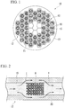
- the superconducting wire 10 in the present embodiment is provided with a core portion 11, a plurality of filaments 12 disposed on the outer peripheral side of the core portion 11, and an outer shell portion 13 disposed on the outer peripheral side of the plurality of filaments 12.
- the filaments 12 described above have a structure in which a wire 15 formed of a superconducting material is surrounded by a superconducting stabilization material 20 in a state of being electrically in contact therewith.
- the wire 15 formed of a superconducting material and the superconducting stabilization material 20 are in a state in which it is possible to conduct electricity.
- the superconducting stabilization material 20 is formed of a copper material which contains one or more types of additive elements selected from Ca, Sr, Ba, and rare earth elements in a total of 3 ppm by mass to 400 ppm by mass, the balance being Cu and inevitable impurities, and a total concentration of the inevitable impurities excluding O, H, C, N, and S which are gas components being 5 ppm by mass to 100 ppm by mass.
- additive elements selected from Ca, Sr, Ba, and rare earth elements in a total of 3 ppm by mass to 400 ppm by mass, the balance being Cu and inevitable impurities, and a total concentration of the inevitable impurities excluding O, H, C, N, and S which are gas components being 5 ppm by mass to 100 ppm by mass.
- the copper material forming the superconducting stabilization material 20 contains inevitable impurities in which an Fe content is 10 ppm by mass or less, a Ni content is 10 ppm by mass or less, an As content is 5 ppm by mass or less, an Ag content is 50 ppm by mass or less, an Sn content is 4 ppm by mass or less, an Sb content is 4 ppm by mass or less, a Pb content is 6 ppm by mass or less, a Bi content is 2 ppm by mass or less, and a P content is 3 ppm by mass or less.
- a ratio Y/X of a total amount of additive elements of one or more types selected from Ca, Sr, Ba, and rare earth elements (Y ppm by mass) to a total amount of S, Se, and Te (X ppm by mass) is in a range of 0.5 ⁇ Y/X ⁇ 100.
- the copper material forming the superconducting stabilization material 20 includes a compound which contains: one or more types of additive elements selected from Ca, Sr, Ba, and rare earth elements; and one or more types of elements selected from S, Se, and Te.
- the superconducting stabilization material 20 has a residual resistance ratio (RRR) of 250 or more.
- additive elements selected from Ca, Sr, Ba, and rare earth elements
- one or more types of additive elements selected from Ca, Sr, Ba, and rare earth elements are elements which are highly reactive with S, Se, and Te, by creating a compound with S, Se, and Te it is possible to suppress S, Se, and Te from forming a solid solution in copper. Due to this, it is possible to sufficiently improve the residual resistance ratio (RRR) of the superconducting stabilization material 20.
- RRR residual resistance ratio
- one or more types of additive elements selected from Ca, Sr, Ba, and rare earth elements are elements which do not easily form a solid solution in copper and which have a small effect of decreasing the residual resistance ratio (RRR) even in a case of forming a solid solution in copper, the residual resistance ratio (RRR) of the superconducting stabilization material 20 does not decrease greatly even in a case where these additive elements are excessively added with respect to the amount of the S, Se, and Te.
- the amount of one or more types of additive elements selected from Ca, Sr, Ba, and rare earth elements is less than 3 ppm by mass, there is a concern that it will not be possible to sufficiently fix S, Se, and Te.
- the amount of one or more types of additive elements selected from Ca, Sr, Ba, and rare earth elements exceeds 400 ppm by mass, there is a concern that coarse precipitates or the like of these additive elements will form, which deteriorates the workability.
- the amount of one or more types of additive elements selected from Ca, Sr, Ba, and rare earth elements is defined within the range of 3 ppm by mass to 400 ppm by mass.
- the amount of one or more types of additive elements selected from Ca, Sr, Ba, and rare earth elements is preferably 3.5 ppm by mass or more, and more preferably 4.0 ppm by mass or more.
- the amount of one or more types of additive elements selected from Ca, Sr, Ba, and rare earth elements is preferably 300 ppm by mass or less, and more preferably 100 ppm by mass or less.
- the concentrations of inevitable impurities excluding gas components (O, H, C, N, and S) are set within the range of 5 ppm by mass to 100 ppm by mass in total.
- the concentration of inevitable impurities excluding the gas components (O, H, C, N, and S) within a range of 5 ppm by mass to 100 ppm by mass in total, it is possible to use high purity copper with a purity of 99 to 99.9999 mass% or oxygen free copper (C10100 and C10200) as a raw material.
- the O concentration is preferably 20 ppm by mass or less, and more preferably 10 ppm by mass or less.
- the O concentration is even more preferably 5 ppm by mass or less.
- the inevitable impurities is preferably 7 ppm by mass or more, and more preferably 10 ppm by mass or more.
- the inevitable impurities is preferably 90 ppm by mass or less, and more preferably 80 ppm by mass or less.
- inevitable impurities in the present embodiment are Fe, Ni, As, Ag, Sn, Sb, Pb, Bi, P, Li, Be, B, F, Na, Mg, Al, Si, Cl, K, Ti, V, Cr, Mn, Nb, Co, Zn, Ga, Ge, Br, Rb, Zr, Mo, Ru, Pd, Cd, In, I, Cs, Hf, Ta, W, Re, Os, Ir, Pt, Au, Hg, Tl, Th, and U.
- the Fe content is defined as 10 ppm by mass or less, the Ni content as 10 ppm by mass or less, the As content as 5 ppm by mass or less, the Ag content as 50 ppm by mass or less, the Sn content as 4 ppm by mass or less, the Sb content as 4 ppm by mass or less, the Pb content as 6 ppm by mass or less, the Bi content as 2 ppm by mass or less, and the P content as 3 ppm by mass or less.
- the Fe content is 4.5 ppm by mass or less, the Ni content as 3 ppm by mass or less, the As content as 3 ppm by mass or less, the Ag content as 38 ppm by mass or less, the Sn content as 3 ppm by mass or less, the Sb content as 1.5 ppm by mass or less, the Pb content as 4.5 ppm by mass or less, the Bi content as 1.5 ppm by mass or less, and the P content as 1.5 ppm by mass or less, and more preferably the Fe content as 3.3 ppm by mass or less, the Ni content as 2.2 ppm by mass or less, the As content as 2.2 ppm by mass or less, the Ag content as 28 ppm by mass or less, the Sn content as 2.2 ppm by mass or less, the Sb content as 1.1 ppm by mass or less, the Pb content as 3.3 ppm
- the lower limit of the amount of Fe, Ni, As, Ag, Sn, Sb, Pb, Bi, and P is 0 ppm by mass.
- one or more types of additive elements selected from Ca, Sr, Ba, and rare earth elements form compounds with elements such as S, Se, and Te.
- the ratio Y/X of the total amount of additive elements (Y ppm by mass) to the total amount of S, Se, and Te (X ppm by mass) is less than 0.5, the amount of additive elements is insufficient, and there is a concern that it may not be possible to sufficiently fix the elements such as S, Se, and Te.
- the ratio Y/X of the total amount of additive elements to the total amount of S, Se, and Te is defined within the range of 0.5 to 100.
- the ratio Y/X of the total amount of additive elements to the total amount of S, Se, and Te is preferably 0.75 or more, and more preferably 1.0 or more.
- the ratio Y/X of the total amount of additive elements to the total amount of S, Se, and Te is preferably 75 or less, and more preferably 50 or less.
- the total amount of S, Se, and Te in the superconducting stabilization material 20 is preferably more than 0 ppm by mass and 25 ppm by mass or less, without being limited thereto.
- one or more types of additive elements selected from Ca, Sr, Ba, and rare earth elements form compounds with elements such as S, Se, and Te so as to suppress elements such as S, Se, and Te from forming solid solutions in the copper.
- compounds containing one or more types of additive elements selected from Ca, Sr, Ba, and rare earth elements and one or more types of elements selected from S, Se, and Te are present, and thereby it is possible to effectively improve the residual resistance ratio (RRR) of the superconducting stabilization material 20.
- RRR residual resistance ratio
- the number density of the compounds when compounds containing one or more types of additive elements selected from Ca, Sr, Ba, and rare earth elements and elements such as S, Se, and Te are present in a number density of 0.001/ ⁇ m 2 or more, it is possible to effectively improve the residual resistance ratio (RRR).
- RRR residual resistance ratio
- the number density is more preferably 0.007/ ⁇ m 2 or more.
- the number density described above relates to a compound having a particle diameter of 0.1 ⁇ m or more.
- the number density of the compound described above is 0.1/ ⁇ m 2 or less, and more preferably 0.09/ ⁇ m 2 or less.
- the number density is even more preferably 0.08/ ⁇ m 2 or less.
- the residual resistance ratio (RRR) of the superconducting stabilization material 20 is 250 or more, the resistance value is low at extremely low temperatures and it is possible to effectively divert the electric current.
- the residual resistance ratio (RRR) is preferably 280 or more, and more preferably 300 or more.
- the residual resistance ratio (RRR) is even more preferably 400 or more.
- the superconducting stabilization material 20 described above is manufactured by a manufacturing process including a melting casting process, a plastic working process, and a heat treatment process.
- a copper wire rod having the composition shown in the present embodiment may be manufactured by a continuous casting rolling method (for example, Southwire Continuous Rod (SCR) system) or the like, and the superconducting stabilization material 20 may be manufactured using this rod as a base material.
- SCR Southwire Continuous Rod
- the continuous casting rolling method referred to here is a process in which a copper wire rod is manufactured using a continuous casting rolling facility provided with a belt-wheel type continuous casting apparatus and a continuous rolling device, and a drawn copper wire is manufactured using this copper wire rod as a material.
- the superconducting wire 10 of the present embodiment formed as described above includes: the wire 15 formed of a superconducting material; and the superconducting stabilization material 20 disposed in contact with the wire 15, and the superconducting stabilization material 20 is formed of a copper material in which one or more types of additive elements selected from Ca, Sr, Ba, and rare earth elements are contained in a total of 3 ppm by mass to 400 ppm by mass in copper where the total concentration of inevitable impurities excluding O, H, C, N, and S which are gas components is 5 ppm by mass to 100 ppm by mass.
- RRR residual resistance ratio
- the superconducting stabilization material being electrically in contact with the wire formed of the superconducting material, even in a case where the normal conducting area A in which the superconducting state is destroyed is generated in the wire 15 formed of the superconducting material, it is possible to effectively divert the electric current to the superconducting stabilization material 20. Therefore, it is possible to suppress the transition of the entire superconducting wire 10 to the normal conducting state, and it is possible to stably use the superconducting wire 10 according to the present embodiment.
- the amounts of Fe, Ni, As, Ag, Sn, Sb, Pb, Bi, and P which influence the residual resistance ratio (RRR) are defined such that the Fe content is 10 ppm by mass or less, the Ni content is 10 ppm by mass or less, the As content is 5 ppm by mass or less, the Ag content is 50 ppm by mass or less, the Sn content is 4 ppm by mass or less, the Sb content is 4 ppm by mass or less, the Pb content is 6 ppm by mass or less, the Bi content is 2 ppm by mass or less, and the P content is 3 ppm by mass or less, it is possible to effectively improve the residual resistance ratio (RRR) of the superconducting stabilization material 20.
- RRR residual resistance ratio
- a ratio Y/X of a total amount of additive elements of one or more types selected from Ca, Sr, Ba, and rare earth elements (Y ppm by mass) to a total amount of S, Se, and Te (X ppm by mass) is within the range of 0.5 ⁇ Y/X ⁇ 100, it is possible to effectively fix S, Se, and Te in copper as a compound with additive elements, and it is possible to effectively suppress decreases in the residual resistance ratio (RRR).
- RRR residual resistance ratio
- the S, Se, and Te present in copper are effectively fixed by a compound with one or more types of additive elements selected from Ca, Sr, Ba, and rare earth elements, and it is possible to effective suppress decreases in the residual resistance ratio (RRR) of the superconducting stabilization material 20 caused by S, Se, and Te.
- RRR residual resistance ratio
- the number density of the compounds having a particle diameter of 0.1 ⁇ m or more is 0.001/ ⁇ m 2 or more, it is possible to effectively fix S, Se, and Te as a compound, and to sufficiently improve the residual resistance ratio (RRR) of the superconducting stabilization material 20.
- the residual resistance ratio (RRR) of the superconducting stabilization material 20 is relatively high at 250 or more, the resistance value at extremely low temperatures is sufficiently low. Therefore, even in a case when the superconducting state is destroyed and a normal conducting area A is generated in the wire 15 formed of the superconducting material, it is possible to effectively divert the electric current to the superconducting stabilization material 20.
- the present invention is not limited thereto but is able to be appropriately modified in a range not departing from the technical idea of the invention.
- the core portion 11 and the outer shell portion 13 forming the superconducting wire 10 may also be formed of a copper material having the same composition as that of the superconducting stabilization material 20 of the present embodiment.
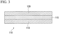
- the superconducting wire 10 having a structure in which the plurality of filaments 12 are bundled is described as an example, but the present invention is not limited thereto, for example, as shown in FIG. 3 , the superconducting wire may be a superconducting wire 110 having a structure in which a superconducting material 115 and a superconducting stabilization material 120 are laminated and disposed on a tape-like substrate 113.
- component analysis was carried out as follows. For elements excluding gas components, glow discharge mass spectrometry was used in a case of being less than 10 ppm by mass and an inductively coupled plasma atomic emission spectrometry was used in a case of being 10 ppm or more. In addition, an infrared absorption method was used for analysis of S. The measured O concentrations were all 10 ppm by mass or less. Here, for the analysis of O, the infrared absorption method was used.
- the particle diameter of the compound was the average length along the major axis of the compound (the maximum length of a straight line which could be drawn in the particle on the condition of not coming into contact with the particle boundary while being drawn) and the minor axis (the maximum length of a straight line which could be drawn in the direction orthogonal to the major axis on the condition of not coming into contact with the particle boundary while being drawn). Then, the number density (number/ ⁇ m 2 ) of the compounds having a particle diameter of 0.1 ⁇ m or more was determined.
- FIG. 4 shows (a) SEM observation results and (b) analysis results (EDX analysis results) of the compound of Example 4
- FIG. 5 shows (a) SEM observation results of the compound and (b) analysis results (EDX analysis results) of Example 10
- FIG. 6 shows (a) SEM observation results and (b) analysis results (EDX analysis results) of the compound of Example 19.
- FIG. 4(b) , FIG. 5(b) , and FIG. 6(b) show the spectra of the compounds marked with "+" in each of FIG. 4(a) , FIG. 5(a) , and FIG. 6(b) .
- Comparative Example 1 the total amount of inevitable impurities excluding the gas components (O, H, C, N, and S) exceeded 100 ppm by mass and the residual resistance ratio (RRR) was relatively low at 106.
- Example 1 to 22 the residual resistance ratio (RRR) was 250 or more, and it was confirmed that Example 1 to 22 is particularly suitable as a superconducting stabilization material.
- a superconducting wire which is able to be stably used and which is provided with a superconducting stabilization material, which is able to be manufactured with a relatively simple and inexpensive manufacturing process and has a sufficiently high residual resistance ratio (RRR).
Landscapes
- Engineering & Computer Science (AREA)
- Mechanical Engineering (AREA)
- Chemical & Material Sciences (AREA)
- Materials Engineering (AREA)
- Metallurgy (AREA)
- Organic Chemistry (AREA)
- Power Engineering (AREA)
- Manufacturing & Machinery (AREA)
- Superconductors And Manufacturing Methods Therefor (AREA)
- Continuous Casting (AREA)
Claims (5)
- Fil supraconducteur comprenant :un fil formé d'un matériau supraconducteur; etun matériau de stabilisation supraconducteur disposé en contact avec le fil,dans lequel le matériau de stabilisation supraconducteur est formé d'un matériau de cuivre qui contient : un ou plusieurs types d'éléments additifs sélectionnés parmi Ca, Sr, Ba, et des éléments de terres rares pour un total de 3 ppm en masse à 400 ppm en masse ; et le reste étant du Cu et des impuretés inévitables, et dans lequel une concentration totale des impuretés inévitables à l'exclusion de O, H, C, N et S qui sont des composants gazeux est de 5 ppm en masse à 100 ppm en masse,dans lequel le matériau de stabilisation supraconducteur est formé du matériau de cuivre avec les impuretés inévitables dans lesquelles une teneur en Fe est de 10 ppm en masse ou moins, une teneur en Ni est de 10 ppm en masse ou moins, une teneur en As est de 5 ppm en masse ou moins, une teneur en Ag est de 50 ppm en masse ou moins, une teneur en Sn est de 4 ppm en masse ou moins, une teneur en Sb est de 4 ppm en masse ou moins, une teneur en Pb est de 6 ppm en masse ou moins, une teneur en Bi est de 2 ppm en masse ou moins, et une teneur en P est de 3 ppm en masse ou moins,dans lequel le matériau de stabilisation supraconducteur est formé du matériau de cuivre dans lequel un rapport Y/X d'une quantité totale d'éléments additifs d'un ou de plusieurs types sélectionnés parmi Ca, Sr, Ba et des éléments de terres rares (Y ppm en masse) sur une quantité totale de S, Se et Te (X ppm en masse) est dans une plage de 0,5 ≤ Y/X ≤ 100.
- Fil supraconducteur selon la revendication 1,
dans lequel le matériau de stabilisation supraconducteur est formé du matériau de cuivre dans lequel est présent un composé qui contient un ou plusieurs types d'éléments additifs sélectionnés parmi Ca, Sr, Ba et des éléments de terres rares et un ou plusieurs types d'éléments sélectionnés parmi S, Se et Te. - Fil supraconducteur selon la revendication 1 ou 2,
dans lequel le matériau de stabilisation supraconducteur a un rapport de résistance résiduelle (RRR) de 250 ou plus. - Fil supraconducteur selon l'une quelconque des revendications 1 à 3,
dans lequel le matériau de stabilisation supraconducteur est fabriqué par un procédé de laminage à coulée continue. - Bobine supraconductrice comprenant :
une partie de fil d'enroulement formée en enroulant le fil supraconducteur selon l'une quelconque des revendications 1 à 4 autour d'une surface extérieure d'un cadre d'enroulement.
Applications Claiming Priority (2)
| Application Number | Priority Date | Filing Date | Title |
|---|---|---|---|
| JP2015001510A JP6056877B2 (ja) | 2015-01-07 | 2015-01-07 | 超伝導線、及び、超伝導コイル |
| PCT/JP2015/085765 WO2016111159A1 (fr) | 2015-01-07 | 2015-12-22 | Fil supraconducteur et bobine supraconductrice |
Publications (3)
| Publication Number | Publication Date |
|---|---|
| EP3243916A1 EP3243916A1 (fr) | 2017-11-15 |
| EP3243916A4 EP3243916A4 (fr) | 2018-05-30 |
| EP3243916B1 true EP3243916B1 (fr) | 2019-03-27 |
Family
ID=56355859
Family Applications (1)
| Application Number | Title | Priority Date | Filing Date |
|---|---|---|---|
| EP15877032.1A Active EP3243916B1 (fr) | 2015-01-07 | 2015-12-22 | Fil supraconducteur et bobine supraconductrice |
Country Status (7)
| Country | Link |
|---|---|
| US (2) | US10964454B2 (fr) |
| EP (1) | EP3243916B1 (fr) |
| JP (1) | JP6056877B2 (fr) |
| KR (1) | KR102450307B1 (fr) |
| CN (2) | CN107002179B (fr) |
| TW (1) | TWI596622B (fr) |
| WO (1) | WO2016111159A1 (fr) |
Families Citing this family (10)
| Publication number | Priority date | Publication date | Assignee | Title |
|---|---|---|---|---|
| JP6056876B2 (ja) * | 2015-01-07 | 2017-01-11 | 三菱マテリアル株式会社 | 超伝導安定化材 |
| JP6056877B2 (ja) | 2015-01-07 | 2017-01-11 | 三菱マテリアル株式会社 | 超伝導線、及び、超伝導コイル |
| JP6299802B2 (ja) | 2016-04-06 | 2018-03-28 | 三菱マテリアル株式会社 | 超伝導安定化材、超伝導線及び超伝導コイル |
| JP6299803B2 (ja) | 2016-04-06 | 2018-03-28 | 三菱マテリアル株式会社 | 超伝導線、及び、超伝導コイル |
| JP7039924B2 (ja) | 2017-10-20 | 2022-03-23 | 株式会社ノーリツ | 熱動弁及び温水暖房装置 |
| EP3705589A4 (fr) * | 2017-10-30 | 2021-08-11 | Mitsubishi Materials Corporation | Matériau de stabilisation de supraconductivité, fil supraconducteur et bobine supraconductrice |
| CN109961899B (zh) * | 2017-12-25 | 2020-12-01 | 西部超导材料科技股份有限公司 | 一种在线热拉制备青铜法Nb3Sn超导线材的方法 |
| JP7380550B2 (ja) * | 2018-12-13 | 2023-11-15 | 三菱マテリアル株式会社 | 純銅板 |
| WO2020203071A1 (fr) * | 2019-03-29 | 2020-10-08 | 三菱マテリアル株式会社 | Matériau de cuivre et élément de dissipation de chaleur |
| CN112322924B (zh) * | 2020-10-16 | 2022-05-20 | 中南大学 | 一种无氧铜、制备方法及应用 |
Family Cites Families (31)
| Publication number | Priority date | Publication date | Assignee | Title |
|---|---|---|---|---|
| JPS5474698A (en) | 1977-11-28 | 1979-06-14 | Univ Tohoku | Superconductive thin band and method of fabricating same |
| JPS6058291B2 (ja) | 1978-01-20 | 1985-12-19 | 住友電気工業株式会社 | 銅合金軟導体およびその製造法 |
| US4233067A (en) | 1978-01-19 | 1980-11-11 | Sumitomo Electric Industries, Ltd. | Soft copper alloy conductors |
| JPS6062009A (ja) | 1983-09-14 | 1985-04-10 | 日立電線株式会社 | Ag入り無酸素銅により安定化された複合超電導体 |
| US4568567A (en) * | 1984-10-09 | 1986-02-04 | Rca Corporation | Method of removing trace quantities of alkali metal impurities from a bialkali-antimonide photoemissive cathode |
| JPS63140052A (ja) * | 1986-12-01 | 1988-06-11 | Hitachi Cable Ltd | 低温軟化性を有する無酸素銅ベ−ス希薄合金及びその用途 |
| JPS63235440A (ja) | 1987-03-23 | 1988-09-30 | Furukawa Electric Co Ltd:The | 銅細線及びその製造方法 |
| JPH01143744A (ja) | 1987-11-30 | 1989-06-06 | Aichi Steel Works Ltd | 酸化物超電導細線の製造方法 |
| JPH02145737A (ja) * | 1988-11-24 | 1990-06-05 | Dowa Mining Co Ltd | 高強度高導電性銅基合金 |
| US5043025A (en) * | 1990-06-12 | 1991-08-27 | Iowa State University Research Foundation, Inc. | High strength-high conductivity Cu--Fe composites produced by powder compaction/mechanical reduction |
| JPH04224662A (ja) * | 1990-12-26 | 1992-08-13 | Hitachi Cable Ltd | 高残留抵抗比銅材の製造方法 |
| JP3047540B2 (ja) | 1991-07-23 | 2000-05-29 | 三菱マテリアル株式会社 | 高い残留抵抗比を有する超電導安定化材用高純度Cu合金 |
| CN1080779A (zh) * | 1993-05-05 | 1994-01-12 | 北京有色金属研究总院 | 极细多芯低温超导线带用的铜合金 |
| US20040266628A1 (en) * | 2003-06-27 | 2004-12-30 | Superpower, Inc. | Novel superconducting articles, and methods for forming and using same |
| JP2005056754A (ja) | 2003-08-06 | 2005-03-03 | Sumitomo Electric Ind Ltd | 超電導線材およびその製造方法 |
| WO2005073434A1 (fr) * | 2004-01-29 | 2005-08-11 | Nippon Mining & Metals Co., Ltd. | Cuivre de purete extreme et processus de production de celui-ci |
| KR101006035B1 (ko) | 2005-06-15 | 2011-01-06 | 제이엑스 닛코 닛세키 킨조쿠 가부시키가이샤 | 초고순도 구리 및 그 제조 방법 그리고 초고순도 구리로이루어지는 본딩 와이어 |
| JP2009507358A (ja) | 2005-07-29 | 2009-02-19 | アメリカン・スーパーコンダクター・コーポレーション | 高温超電導ワイヤ及びコイル |
| WO2007136406A2 (fr) | 2005-11-08 | 2007-11-29 | Supramagnetics, Inc. | Conducteurs composites présentant de meilleures propriétés structurelles et électriques |
| JP4538813B2 (ja) * | 2006-05-29 | 2010-09-08 | Dowaホールディングス株式会社 | 銅基合金材を用いたコネクタ及び充電用ソケット |
| JP5717236B2 (ja) * | 2010-05-12 | 2015-05-13 | 三菱マテリアル株式会社 | 粒子加速器 |
| JP5589753B2 (ja) | 2010-10-20 | 2014-09-17 | 日立金属株式会社 | 溶接部材、及びその製造方法 |
| CN103534370B (zh) | 2011-08-29 | 2015-11-25 | 古河电气工业株式会社 | 铜合金材料及其制造方法 |
| SG190482A1 (en) | 2011-12-01 | 2013-06-28 | Heraeus Materials Tech Gmbh | Doped 4n copper wire for bonding in microelectronics device |
| DE102012205843A1 (de) | 2012-04-11 | 2013-10-17 | Bruker Eas Gmbh | NbTi-Supraleiter mit reduziertem Gewicht |
| JP6101491B2 (ja) | 2012-11-30 | 2017-03-22 | 株式会社フジクラ | 酸化物超電導線材及びその製造方法 |
| JP5752736B2 (ja) | 2013-04-08 | 2015-07-22 | 三菱マテリアル株式会社 | スパッタリング用ターゲット |
| CN103985479B (zh) | 2014-04-28 | 2018-03-30 | 赵遵成 | 一种高温超导涂层导体带材的制备方法 |
| JP6056877B2 (ja) | 2015-01-07 | 2017-01-11 | 三菱マテリアル株式会社 | 超伝導線、及び、超伝導コイル |
| JP6056876B2 (ja) * | 2015-01-07 | 2017-01-11 | 三菱マテリアル株式会社 | 超伝導安定化材 |
| JP6299803B2 (ja) | 2016-04-06 | 2018-03-28 | 三菱マテリアル株式会社 | 超伝導線、及び、超伝導コイル |
-
2015
- 2015-01-07 JP JP2015001510A patent/JP6056877B2/ja active Active
- 2015-12-22 WO PCT/JP2015/085765 patent/WO2016111159A1/fr active Application Filing
- 2015-12-22 EP EP15877032.1A patent/EP3243916B1/fr active Active
- 2015-12-22 CN CN201580066340.7A patent/CN107002179B/zh active Active
- 2015-12-22 KR KR1020177015244A patent/KR102450307B1/ko active IP Right Grant
- 2015-12-22 US US15/540,928 patent/US10964454B2/en active Active
- 2015-12-22 CN CN201810575450.1A patent/CN108766661B/zh active Active
- 2015-12-28 TW TW104144089A patent/TWI596622B/zh active
-
2020
- 2020-10-13 US US17/069,479 patent/US20210225560A1/en not_active Abandoned
Non-Patent Citations (1)
| Title |
|---|
| None * |
Also Published As
| Publication number | Publication date |
|---|---|
| KR20170102224A (ko) | 2017-09-08 |
| US20210225560A1 (en) | 2021-07-22 |
| CN108766661B (zh) | 2020-09-25 |
| CN107002179B (zh) | 2018-11-16 |
| EP3243916A4 (fr) | 2018-05-30 |
| JP6056877B2 (ja) | 2017-01-11 |
| TWI596622B (zh) | 2017-08-21 |
| US10964454B2 (en) | 2021-03-30 |
| CN107002179A (zh) | 2017-08-01 |
| TW201643900A (zh) | 2016-12-16 |
| CN108766661A (zh) | 2018-11-06 |
| JP2016125115A (ja) | 2016-07-11 |
| WO2016111159A1 (fr) | 2016-07-14 |
| US20180005731A1 (en) | 2018-01-04 |
| KR102450307B1 (ko) | 2022-09-30 |
| EP3243916A1 (fr) | 2017-11-15 |
Similar Documents
| Publication | Publication Date | Title |
|---|---|---|
| US20210225560A1 (en) | Superconducting wire and superconducting coil | |
| EP3243917B1 (fr) | Matériau stabilisateur supraconducteur, fil supraconducteur et bobine supraconductrice | |
| US10971278B2 (en) | Superconducting wire and superconducting coil | |
| EP3441485B1 (fr) | Matériau stabilisateur pour supraconducteur, fil supraconducteur et bobine supraconductrice | |
| US11149329B2 (en) | Stabilizer material for superconductor | |
| JP6057007B2 (ja) | 超伝導安定化材、超伝導線及び超伝導コイル | |
| JP6057008B2 (ja) | 超伝導線、及び、超伝導コイル | |
| TW201928073A (zh) | 超導穩定化材料、超導線及超導線圈 |
Legal Events
| Date | Code | Title | Description |
|---|---|---|---|
| STAA | Information on the status of an ep patent application or granted ep patent |
Free format text: STATUS: THE INTERNATIONAL PUBLICATION HAS BEEN MADE |
|
| PUAI | Public reference made under article 153(3) epc to a published international application that has entered the european phase |
Free format text: ORIGINAL CODE: 0009012 |
|
| STAA | Information on the status of an ep patent application or granted ep patent |
Free format text: STATUS: REQUEST FOR EXAMINATION WAS MADE |
|
| 17P | Request for examination filed |
Effective date: 20170704 |
|
| AK | Designated contracting states |
Kind code of ref document: A1 Designated state(s): AL AT BE BG CH CY CZ DE DK EE ES FI FR GB GR HR HU IE IS IT LI LT LU LV MC MK MT NL NO PL PT RO RS SE SI SK SM TR |
|
| AX | Request for extension of the european patent |
Extension state: BA ME |
|
| DAV | Request for validation of the european patent (deleted) | ||
| DAX | Request for extension of the european patent (deleted) | ||
| A4 | Supplementary search report drawn up and despatched |
Effective date: 20180502 |
|
| RIC1 | Information provided on ipc code assigned before grant |
Ipc: H01B 12/02 20060101ALI20180424BHEP Ipc: B22D 11/12 20060101ALI20180424BHEP Ipc: H01B 12/06 20060101ALI20180424BHEP Ipc: C22C 9/00 20060101AFI20180424BHEP Ipc: H01B 12/00 20060101ALI20180424BHEP Ipc: B22D 11/00 20060101ALI20180424BHEP Ipc: H01B 12/04 20060101ALI20180424BHEP Ipc: H01F 6/06 20060101ALI20180424BHEP |
|
| GRAP | Despatch of communication of intention to grant a patent |
Free format text: ORIGINAL CODE: EPIDOSNIGR1 |
|
| STAA | Information on the status of an ep patent application or granted ep patent |
Free format text: STATUS: GRANT OF PATENT IS INTENDED |
|
| INTG | Intention to grant announced |
Effective date: 20181114 |
|
| GRAS | Grant fee paid |
Free format text: ORIGINAL CODE: EPIDOSNIGR3 |
|
| GRAA | (expected) grant |
Free format text: ORIGINAL CODE: 0009210 |
|
| STAA | Information on the status of an ep patent application or granted ep patent |
Free format text: STATUS: THE PATENT HAS BEEN GRANTED |
|
| AK | Designated contracting states |
Kind code of ref document: B1 Designated state(s): AL AT BE BG CH CY CZ DE DK EE ES FI FR GB GR HR HU IE IS IT LI LT LU LV MC MK MT NL NO PL PT RO RS SE SI SK SM TR |
|
| REG | Reference to a national code |
Ref country code: GB Ref legal event code: FG4D |
|
| REG | Reference to a national code |
Ref country code: CH Ref legal event code: EP |
|
| REG | Reference to a national code |
Ref country code: AT Ref legal event code: REF Ref document number: 1113167 Country of ref document: AT Kind code of ref document: T Effective date: 20190415 |
|
| REG | Reference to a national code |
Ref country code: IE Ref legal event code: FG4D |
|
| REG | Reference to a national code |
Ref country code: DE Ref legal event code: R096 Ref document number: 602015027374 Country of ref document: DE |
|
| PG25 | Lapsed in a contracting state [announced via postgrant information from national office to epo] |
Ref country code: LT Free format text: LAPSE BECAUSE OF FAILURE TO SUBMIT A TRANSLATION OF THE DESCRIPTION OR TO PAY THE FEE WITHIN THE PRESCRIBED TIME-LIMIT Effective date: 20190327 Ref country code: SE Free format text: LAPSE BECAUSE OF FAILURE TO SUBMIT A TRANSLATION OF THE DESCRIPTION OR TO PAY THE FEE WITHIN THE PRESCRIBED TIME-LIMIT Effective date: 20190327 Ref country code: NO Free format text: LAPSE BECAUSE OF FAILURE TO SUBMIT A TRANSLATION OF THE DESCRIPTION OR TO PAY THE FEE WITHIN THE PRESCRIBED TIME-LIMIT Effective date: 20190627 |
|
| REG | Reference to a national code |
Ref country code: NL Ref legal event code: MP Effective date: 20190327 |
|
| PG25 | Lapsed in a contracting state [announced via postgrant information from national office to epo] |
Ref country code: LV Free format text: LAPSE BECAUSE OF FAILURE TO SUBMIT A TRANSLATION OF THE DESCRIPTION OR TO PAY THE FEE WITHIN THE PRESCRIBED TIME-LIMIT Effective date: 20190327 Ref country code: GR Free format text: LAPSE BECAUSE OF FAILURE TO SUBMIT A TRANSLATION OF THE DESCRIPTION OR TO PAY THE FEE WITHIN THE PRESCRIBED TIME-LIMIT Effective date: 20190628 Ref country code: HR Free format text: LAPSE BECAUSE OF FAILURE TO SUBMIT A TRANSLATION OF THE DESCRIPTION OR TO PAY THE FEE WITHIN THE PRESCRIBED TIME-LIMIT Effective date: 20190327 Ref country code: RS Free format text: LAPSE BECAUSE OF FAILURE TO SUBMIT A TRANSLATION OF THE DESCRIPTION OR TO PAY THE FEE WITHIN THE PRESCRIBED TIME-LIMIT Effective date: 20190327 Ref country code: NL Free format text: LAPSE BECAUSE OF FAILURE TO SUBMIT A TRANSLATION OF THE DESCRIPTION OR TO PAY THE FEE WITHIN THE PRESCRIBED TIME-LIMIT Effective date: 20190327 Ref country code: BG Free format text: LAPSE BECAUSE OF FAILURE TO SUBMIT A TRANSLATION OF THE DESCRIPTION OR TO PAY THE FEE WITHIN THE PRESCRIBED TIME-LIMIT Effective date: 20190627 |
|
| REG | Reference to a national code |
Ref country code: AT Ref legal event code: MK05 Ref document number: 1113167 Country of ref document: AT Kind code of ref document: T Effective date: 20190327 |
|
| PG25 | Lapsed in a contracting state [announced via postgrant information from national office to epo] |
Ref country code: PT Free format text: LAPSE BECAUSE OF FAILURE TO SUBMIT A TRANSLATION OF THE DESCRIPTION OR TO PAY THE FEE WITHIN THE PRESCRIBED TIME-LIMIT Effective date: 20190727 Ref country code: ES Free format text: LAPSE BECAUSE OF FAILURE TO SUBMIT A TRANSLATION OF THE DESCRIPTION OR TO PAY THE FEE WITHIN THE PRESCRIBED TIME-LIMIT Effective date: 20190327 Ref country code: CZ Free format text: LAPSE BECAUSE OF FAILURE TO SUBMIT A TRANSLATION OF THE DESCRIPTION OR TO PAY THE FEE WITHIN THE PRESCRIBED TIME-LIMIT Effective date: 20190327 Ref country code: RO Free format text: LAPSE BECAUSE OF FAILURE TO SUBMIT A TRANSLATION OF THE DESCRIPTION OR TO PAY THE FEE WITHIN THE PRESCRIBED TIME-LIMIT Effective date: 20190327 Ref country code: EE Free format text: LAPSE BECAUSE OF FAILURE TO SUBMIT A TRANSLATION OF THE DESCRIPTION OR TO PAY THE FEE WITHIN THE PRESCRIBED TIME-LIMIT Effective date: 20190327 Ref country code: IT Free format text: LAPSE BECAUSE OF FAILURE TO SUBMIT A TRANSLATION OF THE DESCRIPTION OR TO PAY THE FEE WITHIN THE PRESCRIBED TIME-LIMIT Effective date: 20190327 Ref country code: SK Free format text: LAPSE BECAUSE OF FAILURE TO SUBMIT A TRANSLATION OF THE DESCRIPTION OR TO PAY THE FEE WITHIN THE PRESCRIBED TIME-LIMIT Effective date: 20190327 Ref country code: AL Free format text: LAPSE BECAUSE OF FAILURE TO SUBMIT A TRANSLATION OF THE DESCRIPTION OR TO PAY THE FEE WITHIN THE PRESCRIBED TIME-LIMIT Effective date: 20190327 |
|
| PG25 | Lapsed in a contracting state [announced via postgrant information from national office to epo] |
Ref country code: PL Free format text: LAPSE BECAUSE OF FAILURE TO SUBMIT A TRANSLATION OF THE DESCRIPTION OR TO PAY THE FEE WITHIN THE PRESCRIBED TIME-LIMIT Effective date: 20190327 Ref country code: SM Free format text: LAPSE BECAUSE OF FAILURE TO SUBMIT A TRANSLATION OF THE DESCRIPTION OR TO PAY THE FEE WITHIN THE PRESCRIBED TIME-LIMIT Effective date: 20190327 |
|
| PG25 | Lapsed in a contracting state [announced via postgrant information from national office to epo] |
Ref country code: AT Free format text: LAPSE BECAUSE OF FAILURE TO SUBMIT A TRANSLATION OF THE DESCRIPTION OR TO PAY THE FEE WITHIN THE PRESCRIBED TIME-LIMIT Effective date: 20190327 Ref country code: IS Free format text: LAPSE BECAUSE OF FAILURE TO SUBMIT A TRANSLATION OF THE DESCRIPTION OR TO PAY THE FEE WITHIN THE PRESCRIBED TIME-LIMIT Effective date: 20190727 |
|
| REG | Reference to a national code |
Ref country code: DE Ref legal event code: R097 Ref document number: 602015027374 Country of ref document: DE |
|
| PG25 | Lapsed in a contracting state [announced via postgrant information from national office to epo] |
Ref country code: DK Free format text: LAPSE BECAUSE OF FAILURE TO SUBMIT A TRANSLATION OF THE DESCRIPTION OR TO PAY THE FEE WITHIN THE PRESCRIBED TIME-LIMIT Effective date: 20190327 |
|
| PLBE | No opposition filed within time limit |
Free format text: ORIGINAL CODE: 0009261 |
|
| STAA | Information on the status of an ep patent application or granted ep patent |
Free format text: STATUS: NO OPPOSITION FILED WITHIN TIME LIMIT |
|
| PG25 | Lapsed in a contracting state [announced via postgrant information from national office to epo] |
Ref country code: SI Free format text: LAPSE BECAUSE OF FAILURE TO SUBMIT A TRANSLATION OF THE DESCRIPTION OR TO PAY THE FEE WITHIN THE PRESCRIBED TIME-LIMIT Effective date: 20190327 |
|
| 26N | No opposition filed |
Effective date: 20200103 |
|
| PG25 | Lapsed in a contracting state [announced via postgrant information from national office to epo] |
Ref country code: TR Free format text: LAPSE BECAUSE OF FAILURE TO SUBMIT A TRANSLATION OF THE DESCRIPTION OR TO PAY THE FEE WITHIN THE PRESCRIBED TIME-LIMIT Effective date: 20190327 |
|
| REG | Reference to a national code |
Ref country code: CH Ref legal event code: PL |
|
| REG | Reference to a national code |
Ref country code: BE Ref legal event code: MM Effective date: 20191231 |
|
| PG25 | Lapsed in a contracting state [announced via postgrant information from national office to epo] |
Ref country code: MC Free format text: LAPSE BECAUSE OF FAILURE TO SUBMIT A TRANSLATION OF THE DESCRIPTION OR TO PAY THE FEE WITHIN THE PRESCRIBED TIME-LIMIT Effective date: 20190327 |
|
| PG25 | Lapsed in a contracting state [announced via postgrant information from national office to epo] |
Ref country code: IE Free format text: LAPSE BECAUSE OF NON-PAYMENT OF DUE FEES Effective date: 20191222 Ref country code: LU Free format text: LAPSE BECAUSE OF NON-PAYMENT OF DUE FEES Effective date: 20191222 |
|
| PG25 | Lapsed in a contracting state [announced via postgrant information from national office to epo] |
Ref country code: CH Free format text: LAPSE BECAUSE OF NON-PAYMENT OF DUE FEES Effective date: 20191231 Ref country code: BE Free format text: LAPSE BECAUSE OF NON-PAYMENT OF DUE FEES Effective date: 20191231 Ref country code: LI Free format text: LAPSE BECAUSE OF NON-PAYMENT OF DUE FEES Effective date: 20191231 |
|
| PG25 | Lapsed in a contracting state [announced via postgrant information from national office to epo] |
Ref country code: CY Free format text: LAPSE BECAUSE OF FAILURE TO SUBMIT A TRANSLATION OF THE DESCRIPTION OR TO PAY THE FEE WITHIN THE PRESCRIBED TIME-LIMIT Effective date: 20190327 |
|
| PG25 | Lapsed in a contracting state [announced via postgrant information from national office to epo] |
Ref country code: HU Free format text: LAPSE BECAUSE OF FAILURE TO SUBMIT A TRANSLATION OF THE DESCRIPTION OR TO PAY THE FEE WITHIN THE PRESCRIBED TIME-LIMIT; INVALID AB INITIO Effective date: 20151222 Ref country code: MT Free format text: LAPSE BECAUSE OF FAILURE TO SUBMIT A TRANSLATION OF THE DESCRIPTION OR TO PAY THE FEE WITHIN THE PRESCRIBED TIME-LIMIT Effective date: 20190327 |
|
| PG25 | Lapsed in a contracting state [announced via postgrant information from national office to epo] |
Ref country code: MK Free format text: LAPSE BECAUSE OF FAILURE TO SUBMIT A TRANSLATION OF THE DESCRIPTION OR TO PAY THE FEE WITHIN THE PRESCRIBED TIME-LIMIT Effective date: 20190327 |
|
| REG | Reference to a national code |
Ref country code: FR Ref legal event code: PLFP Year of fee payment: 8 |
|
| P01 | Opt-out of the competence of the unified patent court (upc) registered |
Effective date: 20230516 |
|
| P02 | Opt-out of the competence of the unified patent court (upc) changed |
Effective date: 20230524 |
|
| PGFP | Annual fee paid to national office [announced via postgrant information from national office to epo] |
Ref country code: GB Payment date: 20231220 Year of fee payment: 9 |
|
| PGFP | Annual fee paid to national office [announced via postgrant information from national office to epo] |
Ref country code: FR Payment date: 20231221 Year of fee payment: 9 Ref country code: FI Payment date: 20231221 Year of fee payment: 9 Ref country code: DE Payment date: 20231214 Year of fee payment: 9 |