EP3241261B1 - Überspannungsschutzanordnung für die informations- und telekommunikationstechnik - Google Patents
Überspannungsschutzanordnung für die informations- und telekommunikationstechnik Download PDFInfo
- Publication number
- EP3241261B1 EP3241261B1 EP15820820.7A EP15820820A EP3241261B1 EP 3241261 B1 EP3241261 B1 EP 3241261B1 EP 15820820 A EP15820820 A EP 15820820A EP 3241261 B1 EP3241261 B1 EP 3241261B1
- Authority
- EP
- European Patent Office
- Prior art keywords
- overvoltage protection
- housing
- protection arrangement
- arrangement according
- connection means
- Prior art date
- Legal status (The legal status is an assumption and is not a legal conclusion. Google has not performed a legal analysis and makes no representation as to the accuracy of the status listed.)
- Active
Links
Images


Classifications
-
- H—ELECTRICITY
- H01—ELECTRIC ELEMENTS
- H01T—SPARK GAPS; OVERVOLTAGE ARRESTERS USING SPARK GAPS; SPARKING PLUGS; CORONA DEVICES; GENERATING IONS TO BE INTRODUCED INTO NON-ENCLOSED GASES
- H01T4/00—Overvoltage arresters using spark gaps
- H01T4/04—Housings
-
- H—ELECTRICITY
- H02—GENERATION; CONVERSION OR DISTRIBUTION OF ELECTRIC POWER
- H02H—EMERGENCY PROTECTIVE CIRCUIT ARRANGEMENTS
- H02H9/00—Emergency protective circuit arrangements for limiting excess current or voltage without disconnection
- H02H9/04—Emergency protective circuit arrangements for limiting excess current or voltage without disconnection responsive to excess voltage
- H02H9/044—Physical layout, materials not provided for elsewhere
-
- H—ELECTRICITY
- H01—ELECTRIC ELEMENTS
- H01R—ELECTRICALLY-CONDUCTIVE CONNECTIONS; STRUCTURAL ASSOCIATIONS OF A PLURALITY OF MUTUALLY-INSULATED ELECTRICAL CONNECTING ELEMENTS; COUPLING DEVICES; CURRENT COLLECTORS
- H01R9/00—Structural associations of a plurality of mutually-insulated electrical connecting elements, e.g. terminal strips or terminal blocks; Terminals or binding posts mounted upon a base or in a case; Bases therefor
- H01R9/22—Bases, e.g. strip, block, panel
- H01R9/24—Terminal blocks
- H01R9/26—Clip-on terminal blocks for side-by-side rail- or strip-mounting
-
- H—ELECTRICITY
- H01—ELECTRIC ELEMENTS
- H01T—SPARK GAPS; OVERVOLTAGE ARRESTERS USING SPARK GAPS; SPARKING PLUGS; CORONA DEVICES; GENERATING IONS TO BE INTRODUCED INTO NON-ENCLOSED GASES
- H01T4/00—Overvoltage arresters using spark gaps
- H01T4/06—Mounting arrangements for a plurality of overvoltage arresters
-
- H—ELECTRICITY
- H02—GENERATION; CONVERSION OR DISTRIBUTION OF ELECTRIC POWER
- H02H—EMERGENCY PROTECTIVE CIRCUIT ARRANGEMENTS
- H02H9/00—Emergency protective circuit arrangements for limiting excess current or voltage without disconnection
- H02H9/04—Emergency protective circuit arrangements for limiting excess current or voltage without disconnection responsive to excess voltage
- H02H9/045—Emergency protective circuit arrangements for limiting excess current or voltage without disconnection responsive to excess voltage adapted to a particular application and not provided for elsewhere
-
- H—ELECTRICITY
- H05—ELECTRIC TECHNIQUES NOT OTHERWISE PROVIDED FOR
- H05K—PRINTED CIRCUITS; CASINGS OR CONSTRUCTIONAL DETAILS OF ELECTRIC APPARATUS; MANUFACTURE OF ASSEMBLAGES OF ELECTRICAL COMPONENTS
- H05K1/00—Printed circuits
- H05K1/02—Details
- H05K1/14—Structural association of two or more printed circuits
- H05K1/144—Stacked arrangements of planar printed circuit boards
-
- H—ELECTRICITY
- H05—ELECTRIC TECHNIQUES NOT OTHERWISE PROVIDED FOR
- H05K—PRINTED CIRCUITS; CASINGS OR CONSTRUCTIONAL DETAILS OF ELECTRIC APPARATUS; MANUFACTURE OF ASSEMBLAGES OF ELECTRICAL COMPONENTS
- H05K5/00—Casings, cabinets or drawers for electric apparatus
- H05K5/0026—Casings, cabinets or drawers for electric apparatus provided with connectors and printed circuit boards [PCB], e.g. automotive electronic control units
-
- H—ELECTRICITY
- H05—ELECTRIC TECHNIQUES NOT OTHERWISE PROVIDED FOR
- H05K—PRINTED CIRCUITS; CASINGS OR CONSTRUCTIONAL DETAILS OF ELECTRIC APPARATUS; MANUFACTURE OF ASSEMBLAGES OF ELECTRICAL COMPONENTS
- H05K5/00—Casings, cabinets or drawers for electric apparatus
- H05K5/02—Details
- H05K5/0247—Electrical details of casings, e.g. terminals, passages for cables or wiring
-
- H—ELECTRICITY
- H05—ELECTRIC TECHNIQUES NOT OTHERWISE PROVIDED FOR
- H05K—PRINTED CIRCUITS; CASINGS OR CONSTRUCTIONAL DETAILS OF ELECTRIC APPARATUS; MANUFACTURE OF ASSEMBLAGES OF ELECTRICAL COMPONENTS
- H05K1/00—Printed circuits
- H05K1/18—Printed circuits structurally associated with non-printed electric components
- H05K1/181—Printed circuits structurally associated with non-printed electric components associated with surface mounted components
-
- H—ELECTRICITY
- H05—ELECTRIC TECHNIQUES NOT OTHERWISE PROVIDED FOR
- H05K—PRINTED CIRCUITS; CASINGS OR CONSTRUCTIONAL DETAILS OF ELECTRIC APPARATUS; MANUFACTURE OF ASSEMBLAGES OF ELECTRICAL COMPONENTS
- H05K2201/00—Indexing scheme relating to printed circuits covered by H05K1/00
- H05K2201/04—Assemblies of printed circuits
- H05K2201/042—Stacked spaced PCBs; Planar parts of folded flexible circuits having mounted components in between or spaced from each other
-
- H—ELECTRICITY
- H05—ELECTRIC TECHNIQUES NOT OTHERWISE PROVIDED FOR
- H05K—PRINTED CIRCUITS; CASINGS OR CONSTRUCTIONAL DETAILS OF ELECTRIC APPARATUS; MANUFACTURE OF ASSEMBLAGES OF ELECTRICAL COMPONENTS
- H05K2201/00—Indexing scheme relating to printed circuits covered by H05K1/00
- H05K2201/09—Shape and layout
- H05K2201/09009—Substrate related
- H05K2201/09027—Non-rectangular flat PCB, e.g. circular
-
- H—ELECTRICITY
- H05—ELECTRIC TECHNIQUES NOT OTHERWISE PROVIDED FOR
- H05K—PRINTED CIRCUITS; CASINGS OR CONSTRUCTIONAL DETAILS OF ELECTRIC APPARATUS; MANUFACTURE OF ASSEMBLAGES OF ELECTRICAL COMPONENTS
- H05K2201/00—Indexing scheme relating to printed circuits covered by H05K1/00
- H05K2201/10—Details of components or other objects attached to or integrated in a printed circuit board
- H05K2201/10227—Other objects, e.g. metallic pieces
- H05K2201/10287—Metal wires as connectors or conductors
-
- H—ELECTRICITY
- H05—ELECTRIC TECHNIQUES NOT OTHERWISE PROVIDED FOR
- H05K—PRINTED CIRCUITS; CASINGS OR CONSTRUCTIONAL DETAILS OF ELECTRIC APPARATUS; MANUFACTURE OF ASSEMBLAGES OF ELECTRICAL COMPONENTS
- H05K2201/00—Indexing scheme relating to printed circuits covered by H05K1/00
- H05K2201/10—Details of components or other objects attached to or integrated in a printed circuit board
- H05K2201/10227—Other objects, e.g. metallic pieces
- H05K2201/10325—Sockets, i.e. female type connectors comprising metallic connector elements integrated in, or bonded to a common dielectric support
-
- H—ELECTRICITY
- H05—ELECTRIC TECHNIQUES NOT OTHERWISE PROVIDED FOR
- H05K—PRINTED CIRCUITS; CASINGS OR CONSTRUCTIONAL DETAILS OF ELECTRIC APPARATUS; MANUFACTURE OF ASSEMBLAGES OF ELECTRICAL COMPONENTS
- H05K2201/00—Indexing scheme relating to printed circuits covered by H05K1/00
- H05K2201/10—Details of components or other objects attached to or integrated in a printed circuit board
- H05K2201/10227—Other objects, e.g. metallic pieces
- H05K2201/10393—Clamping a component by an element or a set of elements
-
- H—ELECTRICITY
- H05—ELECTRIC TECHNIQUES NOT OTHERWISE PROVIDED FOR
- H05K—PRINTED CIRCUITS; CASINGS OR CONSTRUCTIONAL DETAILS OF ELECTRIC APPARATUS; MANUFACTURE OF ASSEMBLAGES OF ELECTRICAL COMPONENTS
- H05K5/00—Casings, cabinets or drawers for electric apparatus
- H05K5/0021—Side-by-side or stacked arrangements
Definitions
- the invention relates to an overvoltage protection arrangement for information and telecommunications technology, consisting of a housing with means for top-hat rail mounting on the housing base, overvoltage protection elements located in the housing, electrical connection means and at least one printed circuit board as a wiring support for the overvoltage protection elements, further consisting of a housing with a bar-shaped base body and a protruding head part according to claim 1.
- Surge protection arrangements for information technology e.g. As divisible arrester for top-hat rail mounting, are known under the product name Blitzductor, manufactured and offered by DEHN + S ⁇ HNE GmbH + Co. KG.
- surge arresters are known in the prior art and are located in a housing which permits top-hat rail mounting.
- the actual overvoltage protection elements, decoupling resistors, diodes, inductors, but also, if necessary, control circuits are located in the housing, which has the shape of an inverted T.
- the connection on the input and output side is made using screw terminals that are accessible from the top of the bar-shaped base body of the housing.
- a bus-compatible, stackable connection and / or function module for the control and / or monitoring of technical processes or for building automation, which has a disk-like or block-like structure.
- This previously known function module can be used with Further modules are put together to form a connection system and has at least one base terminal body and an attachable housing.
- a printed circuit board and / or a lead frame or, in one embodiment, a busbar arrangement are located in the housing.
- there is at least one bus conductor contact for forwarding at least one energy or data bus in the direction of the sequence.
- Connection or function modules can be connected separately, with at least one of these function modules having signal matching electronics in addition to an I / O electronics of the corresponding connection or function module. At least one of the connectable connection or function modules should have a connection level, the connections of which are connected to one another in such a conductive manner that a terminal block function can be implemented.
- the overvoltage protection arrangement comprises a housing with means for top-hat rail mounting formed on the housing base.
- surge protection elements e.g. Varistors, gas arresters, protective diodes, resistors or the like.
- Electrical connection means are provided on or in the housing and at least one printed circuit board is provided as a wiring support for the overvoltage protection elements.
- the housing has e.g. a side view of the shape of an approximate, upside down T corresponds. Modifications to this housing shape are within the meaning of the invention.
- the housing has a substantially bar-shaped base body and a head part projecting from the base body, the electrical connection means e.g. are accessible or can be actuated via the top or front of the bar-shaped base body.
- a first and a second printed circuit board are formed, which are spaced apart from one another on the inner sides of the side walls of the housing.
- the resulting space between the printed circuit boards forms a volume for the electrical connection means in the form of electrical connection terminals, connection sockets and / or connection plugs.
- the first connection means are horizontal and the second connection means vertical Level of the bar-shaped base body accessible.
- the surface shape of the circuit boards corresponds to the shape of the housing or is approximated to this housing shape. In this way, the largest possible area, which results from the shape of the housing, is used by the printed circuit boards.
- the spaced arrangement of the printed circuit boards makes it possible, when contacted directly with the printed circuit boards, to fix necessary terminals for a wire connection, but also coaxial connectors, and to make electrical contact.
- the first connection means are designed as lockable socket strips, fixed on the printed circuit boards, for clamping wires.
- the second connection means are designed as coaxial plugs or sockets.
- the horizontal plane of the bar-shaped base body is formed at least in the area of the connection means as an inclined surface for angled guiding and receiving connection wires when the surge protection device is arranged under a distributor cover.
- the overvoltage protection arrangement according to the invention is designed to be arranged in a row.
- a closable opening is provided on the head part of the respective housing in the area of the printed circuit boards, which allows access to a printed circuit board section, in particular to a printed circuit board cable.
- a plug-in element can be attached by means of the openings, which connects the respective devices mechanically and / or electrically.
- the plug-in element is realized as a molded part, each of which has a complementary extension which is placed on the opening contour.
- the plug element itself can be conductive or have a conductive section to provide the desired electrical connection, e.g. to create for a bus system.
- the plug-in element can be designed as an electrical connecting bridge.
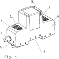
- an overvoltage protection arrangement which has a housing which has the shape of an upside-down T.
- the housing has a bar-shaped base body 1 and a protruding head part 2.
- a recess 3 is provided for the purpose of top-hat rail mounting of the surge protection arrangement.
- a first level on the bar-shaped base body 1 is referred to as the horizontal level 4 and a second level as the horizontal level 5.
- Electrical connection means 6 as well as electrical connection means 7 on the vertical level 5 are accessible or arranged both on the horizontal level 4.
- the first connection means 6 are designed as terminals for wire connection.
- the horizontal plane 4 is inclined, i.e. formed as an inclined surface so that an optimal insertion of connection lines is possible and the connection lines find space under a distributor cover, not shown.
- a connection means 7 a BNC socket.
- Further designs can be provided as RJ sockets, Sub-D plug sockets or the like.
- level 9 is used for the arrangement of a terminal, which is described below, in alignment with the neighboring device when stringing together
- Various surge protection devices for example for connecting a bus / communication line for data exchange between correspondingly adjacent devices.
- the representations according to the Fig. 2 and 3rd show that two spaced printed circuit boards 10 and 11 are arranged within the housing, which have a surface shape which corresponds essentially to the longitudinal sectional surface of the housing.
- the printed circuit boards also carry the actual overvoltage protection elements 12, for example varistors, and serve to fix function displays 13, for example designed as light-emitting diodes.
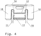
- the plug element 14 can, as in Fig. 4 it becomes clear that it is designed as a molded part which has extensions 16 which are adapted to the opening 15 in the opening part in the head part 9 of the housing.
- the plug element 14 is provided with a conductive contour or a conductive section 17, the desired electrical connection between the printed circuit boards 10 and 11 can be realized.
- the plug element 14 consists of the two pin-shaped extensions 16, which are connected via a web.
- the respective opening 15 in the head part 9 of the corresponding housing is adapted to this plug element contour.
- the connector can therefore be designed in such a way that the contour of the plug-in element and the complementary design as a housing contour at the same time result in mechanical locking between adjacent devices. This will improve the stability of the overall arrangement reached. After removing the plug-in element or the corresponding plug-in elements 14, a corresponding device can be removed from the assembly. A loosening of wires or cables is therefore not necessary.
- the Fig. 7 shows an overvoltage protection arrangement according to the invention with a partially broken housing, arranged on a top-hat rail 18.
- a partially broken housing arranged on a top-hat rail 18.
- the printed circuit boards 10; 11 For contacting with the top-hat rail, there is the possibility of the printed circuit boards 10; 11 to connect mechanically via a contact element 19 and to make electrical contact.
- the mentioned contact element 19 is provided in the lower part of the housing, which connects the printed circuit boards 10 and 11 to the top-hat rail 18.
- good mechanical strength of the printed circuit boards in the housing with a seat on the top-hat rail 18 is achieved.
- the arrangement in the lower housing part can be fixed via latching elements 20 on the contact element 19.
Landscapes
- Engineering & Computer Science (AREA)
- Microelectronics & Electronic Packaging (AREA)
- Emergency Protection Circuit Devices (AREA)
- Connections Arranged To Contact A Plurality Of Conductors (AREA)
- Coupling Device And Connection With Printed Circuit (AREA)
- Protection Of Static Devices (AREA)
Description
- Die Erfindung betrifft eine Überspannungsschutzanordnung für die Informations- und Telekommunikationstechnik, bestehend aus einem Gehäuse mit am Gehäuseboden ausgebildeten Mitteln zur Hutschienenmontage, im Gehäuse befindlichen Überspannungsschutzelementen, elektrischen Anschlussmitteln sowie mindestens einer Leiterplatte als Verdrahtungsträger für die Überspannungsschutzelemente, weiterhin bestehend aus einem Gehäuse mit einem balkenförmigen Grundkörper und einem hervorspringenden Kopfteil gemäß Anspruch 1.
- Überspannungsschutzanordnungen für die Informationstechnik, z.B. als teilbarer Ableiter für die Hutschienenmontage, sind unter der Produktbezeichnung Blitzductor, hergestellt und angeboten von der Firma DEHN + SÖHNE GmbH + Co. KG, bekannt.
- Zum wirtschaftlichen Schutz von mehradrigen Signalwegen gehören Überspannungsableiter zum bekannten Stand der Technik, die in einem Gehäuse befindlich sind, das eine Hutschienenmontage gestattet. Dabei befinden sich in dem Gehäuse, das die Gestalt eines auf dem Kopf stehenden T besitzt, die eigentlichen Überspannungsschutzelemente, Entkopplungswiderstände, Dioden, Induktivitäten, aber auch bei Notwendigkeit Ansteuerschaltungen. Der Anschluss eingangs- und ausgangsseitig erfolgt wie beispielsweise bei den Typen Blitzductor BVT über Schraubklemmen, die von der Oberseite des balkenförmigen Grundkörpers des Gehäuses zugänglich sind.
- Aus der
DE 20 2011 000 835 U1 ist ein busfähiges, anreihbares Anschluss- und/oder Funktionsmodul zur Steuerung und/oder Überwachung technischer Prozesse oder zur Gebäudeautomatisierung vorbekannt, das einen scheiben- oder blockartigen Aufbau besitzt. Dieses vorbekannte Funktionsmodul kann mit weiteren Modulen zu einem Anschlusssystem zusammengestellt werden und weist mindestens einen Basisklemmenkörper und ein aufsetzbares Gehäuse auf. Im Gehäuse befinden sich eine Leiterplatte und/oder ein Stanzgitter bzw. bei einer Ausführungsform eine Stromschienenanordnung. Darüber hinaus ist wenigsten ein Busleiterkontakt zur Weiterleitung wenigstens eines Energie- oder Datenbusses in Anreihrichtung vorhanden. Am Gehäuse nachDE 20 2011 000 835 U1 können Anschluss- oder Funktionsbausteine separat angeschlossen werden, wobei mindestens einer dieser Funktionsbausteine eine Signalanpassungselektronik zusätzlich zu einer I/O-Elektronik des entsprechenden Anschluss- oder Funktionsmoduls besitzt. Wenigstens eines der anreihbaren Anschluss- oder Funktionsmodule soll eine Anschlussebene besitzen, deren Anschlüsse derart leitend miteinander verbunden sind, dass eine Reihenklemmenfunktion realisierbar ist. - Es hat sich gezeigt, dass bei den bekannten Überspannungsschutzanordnungen für die Informations- und Telekommunikationstechnik der Anschluss der zu schützenden Geräte über vorhandene Drahtklemmen einen erheblichen Aufwand darstellt, wobei oftmals die Zahl der anzuschließenden Drähte eine Vielzahl von Schraubklemmen erfordert, die nur schlecht in ein entsprechendes Gehäuse integriert werden kann. Bei der Notwendigkeit einer Durchverbindung einer Bus-/Kommunikationsleitung für den Datenaustausch zwischen mehreren, nebeneinander angeordneten Geräten war es im Bereich des Überspannungsschutzes bisher notwendig, eine diesbezüglich separate Kabelverbindung auszuführen. Beim Austausch entsprechender Geräte bzw. zu Mess- und Prüfvorgängen ist es dadurch erforderlich, weitere Klemmen zu lösen mit der Folge einer aufwendigeren Handhabung.
- Aus dem Vorgenannten ist es daher Aufgabe der Erfindung, eine weiterentwickelte Überspannungsschutzanordnung für die Informations- und Telekommunikationstechnik, bestehend aus einem Gehäuse mit am Gehäuseboden ausgebildeten Mitteln zur Hutschienenmontage und im Gehäuse befindlichen Überspannungsschutzelementen nebst elektrischen Anschlussmitteln anzugeben, welche zum einen einen optimalen Bauraum für die erforderlichen elektrischen und mechanischen Mittel zur Verfügung stellt und die darüber hinaus neue Möglichkeiten zur Kontaktierung bietet, so dass insgesamt der Handhabungs- und Montageaufwand beim Einsatz derartiger Überspannungsschutzanordnungen bzw. -geräte reduziert ist.
- Die Lösung der Aufgabe der Erfindung erfolgt mit der Merkmalskombination nach Anspruch 1, wobei die Unteransprüche mindestens zweckmäßige Ausgestaltungen und Weiterbildungen darstellen.
- Es wird demnach von einer Überspannungsschutzanordnung für die Informations- und Telekommunikationstechnik ausgegangen. Hierunter sind alle Applikationen auch im Bereich der Gebäudetechnik, der Prozesstechnik und der elektronischen Datenübertragung zu verstehen, ohne dass andere Anwendungsbereiche ausgeschlossen werden sollen.
- Die Überspannungsschutzanordnung umfasst ein Gehäuse mit am Gehäuseboden ausgebildeten Mitteln zur Hutschienenmontage.
- Darüber hinaus befinden sich im Gehäuse die eigentlichen Überspannungsschutzelemente, z.B. Varistoren, Gasableiter, Schutzdioden, Widerstände oder dergleichen. Am bzw. im Gehäuse sind elektrische Anschlussmittel vorhanden und es ist mindestens eine Leiterplatte als Verdrahtungsträger für die Überspannungsschutzelemente vorgesehen.
- Das Gehäuse weist z.B. eine Seitenansicht auf, die der Gestalt eines angenäherten, auf dem Kopf stehenden T entspricht. Abwandlungen dieser Gehäuseform liegen im Sinne der Erfindung.
- Das Gehäuse besitzt einen im Wesentlichen balkenförmigen Grundkörper und einen vom Grundkörper vorspringenden Kopfteil, wobei die elektrischen Anschlussmittel z.B. über die Oberseite oder Vorderseite des balkenförmigen Grundkörpers zugänglich sind oder betätigt werden können.
- Erfindungsgemäß ist eine erste und eine zweite Leiterplatte ausgebildet, die voneinander beabstandet jeweils an den Innenseiten der Seitenwände des Gehäuses befindlich sind.
- Der sich ergebende Abstandsraum zwischen den Leiterplatten bildet ein Raumvolumen für die elektrischen Anschlussmittel in Form von elektrischen Anschlussklemmen, Anschlussbuchsen und/oder Anschlusssteckern. Erste Anschlussmittel sind in horizontaler und zweite Anschlussmittel in vertikaler Ebene des balkenförmigen Grundkörpers zugänglich. Weiterhin entspricht die Flächenform der Leiterplatten der Form des Gehäuses bzw. ist dieser Gehäuseform angenähert. Damit wird quasi die größtmögliche Fläche, die sich durch die Gehäusegestalt ergibt, durch die Leiterplatten ausgenutzt.
- Die beabstandete Anordnung der Leiterplatten ermöglicht es, unmittelbar mit den Leiterplatten kontaktiert, erforderliche Klemmen für einen Drahtanschluss, aber auch koaxiale Steckverbinder zu fixieren und elektrisch zu kontaktieren.
- Erfindungsgemäß sind die ersten Anschlussmittel als auf den Leiterplatten fixierte, verriegelbare Buchsenleisten zum Klemmen von Drähten ausgebildet.
- Bei einer weiteren Ausführungsform sind die zweiten Anschlussmittel als koaxiale Stecker oder Buchsen ausgeführt.
- Bei einer bevorzugten Weiterbildung der Erfindung ist die horizontale Ebene des balkenförmigen Grundkörpers mindestens im Bereich der Anschlussmittel als Schrägfläche zur abgewinkelten Führung und Aufnahme von Anschlussdrähten bei Anordnung des Überspannungsschutzgeräts unter einer Verteilerabdeckung ausgebildet.
- Die erfindungsgemäße Überspannungsschutzanordnung ist aneinanderreihbar ausgebildet.
- Diesbezüglich ist am Kopfteil des jeweiligen Gehäuses jeweils im Bereich der Leiterplatten eine verschließbare Öffnung vorgesehen, welche Zugang zu einem Leiterplattenabschnitt, insbesondere zu einem Leiterplattenzug gewährt. Bei mindestens zwei aneinandergereihten Überspannungsschutzgeräten ist mittels der Öffnungen ein Steckelement anbringbar, welches die jeweiligen Geräte mechanisch und/oder elektrisch verbindet.
- Das Steckelement ist als Formteil realisiert, welches jeweils einen auf die Öffnungskontur abgestellten, dieser komplementären Fortsatz aufweist.
- Das Steckelement selbst kann leitfähig sein oder einen leitfähigen Abschnitt besitzen, um die gewünschte elektrische Verbindung, z.B. für ein Bussystem zu schaffen. Insofern ist das Steckelement als elektrische Verbindungsbrücke ausführbar.
- Im Bereich der dem Gehäuseboden zugewandten Enden der Leiterplatten sind diese über ein gemeinsames Kontaktelement mechanisch und elektrisch verbunden, wobei über das gemeinsame Kontaktelement eine elektrische Verbindung zur Hutschiene zum Zweck der Schaffung einer Erdverbindung herstellbar ist.
- Die Erfindung soll nachstehend anhand von Ausführungsbeispielen und unter Zuhilfenahme von Figuren näher erläutert werden.
- Hierbei zeigen:
- Fig. 1
- eine perspektivische Darstellung der Überspannungsschutzanordnung mit Gehäuse in Gestalt eines auf dem Kopf stehenden T;
- Fig. 2
- eine Darstellung ähnlich derjenigen nach
Fig. 1 , jedoch mit frei zugänglichem Blick auf die die Gehäuseform approximierenden, beabstandeten Leiterplatten nebst Anschlussmitteln; - Fig. 3
- eine Darstellung von drei aneinandergereihten Überspannungsschutzanordnungen (unter Weglassung von Teilen des Gehäuses);
- Fig. 4
- eine vergrößerte Darstellung des als Verbindungsbrücke ausgebildeten Steckelements, welches bereits bei der
Fig. 3 erkennbar ist; - Fig. 5
- eine perspektivische Darstellung (Ansicht von oben) von drei aneinandergereihten Überspannungsschutzanordnungen, die über Steckelemente verbunden sind;
- Fig. 6
- eine Detaildarstellung zweier aneinandergereihter Überspannungsschutzanordnungen mit im Kopfteil des Gehäuses jeweils befindlicher verschließbarer Öffnung und im Öffnungsabschnitt erkennbarem Teil einer jeweiligen Leiterplatte;
- Fig. 7
- eine perspektivische Darstellung der Anordnung eines Überspannungsschutzgeräts auf einer Hutschiene mit teilweggebrochenem Gehäuse und
- Fig. 8
- eine Detaildarstellung der Leiterplatten mit gemeinsamem Kontaktelement.
- Gemäß Ausführungsbeispiel wird von einer Überspannungsschutzanordnung ausgegangen, die ein Gehäuse besitzt, das die Gestalt eines auf dem Kopf stehenden T besitzt. Das Gehäuse besitzt einen balkenförmigen Grundkörper 1 und einen hervorspringenden Kopfteil 2.
- Am Boden des balkenförmigen Grundkörpers 1 ist ein Rücksprung 3 zum Zweck der Hutschienenmontage der Überspannungsschutzanordnung vorgesehen.
- Eine erste Ebene am balkenförmigen Grundkörper 1 wird als horizontale Ebene 4 und eine zweite Ebene als horizontale Ebene 5 bezeichnet. Sowohl auf der horizontalen Ebene 4 sind elektrische Anschlussmittel 6 als auch auf der vertikalen Ebene 5 elektrische Anschlussmittel 7 zugänglich bzw. angeordnet.
- Bei einer bevorzugten Ausführungsform sind die ersten Anschlussmittel 6 als Klemmen zum Drahtanschluss ausgebildet. Die horizontale Ebene 4 ist geneigt, d.h. als Schrägfläche ausgebildet, so dass eine optimale Einführung von Anschlussleitungen möglich ist und die Anschlussleitungen Platz unter einer nicht gezeigten Verteilerabdeckung finden.
- In der vertikalen Ebene 5 (Ebene 2) können z.B. Buchsen oder Stecker angeordnet sein. Die Darstellung nach
Fig. 1 zeigt als Anschlussmittel 7 eine BNC-Buchse. Weitere Ausführungen können als RJ-Buchsen, Sub-D-Steckerbuchsen oder dergleichen vorgesehen sein. - Die vorerwähnte Schrägfläche ist in der
Fig. 1 mit dem Bezugszeichen 8 symbolisiert. - Eine weitere Ebene 9 (Ebene 3) dient der im Folgenden noch beschriebenen Anordnung einer Klemme in Ausrichtung zum Nachbargerät beim Aneinanderreihen verschiedener Überspannungsschutzanordnungen, z.B. zur Durchverbindung einer Bus-/Kommunikationsleitung für den Datenaustausch zwischen entsprechend nebeneinander befindlichen Geräten.
- Die Darstellungen nach den
Fig. 2 und3 zeigen, dass innerhalb des Gehäuses zwei beabstandete Leiterplatten 10 und 11 angeordnet sind, die eine Flächenform aufweisen, die im Wesentlichen der Längsschnittfläche des Gehäuses entspricht. Im Raum zwischen den Leiterplatten 10 und 11 sind z.B. jeweils Klemmen 6 für den Drahtanschluss bzw. ein Stecker / eine Buchse 7 zum Anschluss eines Koaxialleiters befindlich. Die Leiterplatten tragen darüber hinaus die eigentlichen Überspannungsschutzelemente 12, z.B. Varistoren, und dienen dem Fixieren von Funktionsanzeigen 13, z.B. ausgebildet als lichtemittierende Dioden. - Wie aus den
Fig. 3 und4 ersichtlich, kann durch die Anordnung der Leiterplatten 10; 11 seitlich an der jeweiligen Gehäuseinnenwandung über einen Leiterplatten-Steckverbinder 14 eine elektrische Verbindung zwischen benachbarten Geräten hergestellt werden, um einen Datenaustausch zu realisieren oder aber auch eine Stromversorgung zu ermöglichen. - Das Steckelement 14 kann, wie in
Fig. 4 deutlich wird, als Formteil ausgeführt werden, welches auf die Öffnungskontur im Kopfteil 9 des Gehäuses befindliche Öffnung 15 angepasste Fortsätze 16 aufweist. - Ist z.B. das Steckelement 14 mit einer leitfähigen Kontur oder einem leitfähigen Abschnitt 17 versehen, kann die gewünschte elektrische Verbindung zwischen den Leiterplatten 10 und 11 realisiert werden.
- Beim gezeigten Beispiel besteht das Steckelement 14 aus den zwei stiftförmigen Fortsätzen 16, die über einen Steg verbunden sind. Die jeweilige Öffnung 15 im Kopfteil 9 des entsprechenden Gehäuses ist dieser Steckelemente-Kontur entsprechend angepasst.
- Der Verbinder ist demnach so ausführbar, dass über die Kontur des Steckelements und der komplementären Ausbildung als Gehäusekontur gleichzeitig eine mechanische Verrastung zwischen benachbarten Geräten erfolgt. Hierdurch wird eine Verbesserung der Stabilität der Gesamtanordnung erreicht. Nach Abziehen des Steckelements bzw. der entsprechenden Steckelemente 14 kann ein entsprechendes Gerät aus dem Verband herausgelöst werden. Ein Lösen von Drähten oder Kabeln ist insofern nicht erforderlich.
- Die
Fig. 7 zeigt eine erfindungsgemäße Überspannungsschutzanordnung mit teilweggebrochenem Gehäuse, angeordnet auf einer Hutschiene 18. Zur Kontaktierung mit der Hutschiene besteht die Möglichkeit, die Leiterplatten 10; 11 über ein Kontaktelement 19 mechanisch zu verbinden und elektrisch zu kontaktieren. - Insofern ist im Unterteil des Gehäuses das erwähnte Kontaktelement 19 vorgesehen, welches die Leiterplatten 10 und 11 mit der Hutschiene 18 verbindet. Ergänzend wird mit Blick auf dieses Lösungselement eine gute mechanische Festigkeit der Leiterplatten im Gehäuse mit Sitz auf der Hutschiene 18 erreicht. Über Rastelemente 20 am Kontaktelement 19 kann die Anordnung im Gehäuseunterteil fixiert werden.
Claims (10)
- Überspannungsschutzanordnung für die Informations- und Telekommunikationstechnik, bestehend aus einem Gehäuse mit am Gehäuseboden ausgebildeten Mitteln (3) zur Hutschienenmontage, im Gehäuse befindlichen Überspannungsschutzelementen (12), elektrischen Anschlussmitteln (6; 7) sowie Leiterplatten (10; 11) als Verdrahtungsträger für die Überspannungsschutzelemente (12), weiterhin mit einer Gestalt des Gehäuses mit einem balkenförmigen Grundkörper (1) und einem hervorspringenden Kopfteil (2), wobei
eine erste (10) und eine zweite (11) Leiterplatte voneinander beabstandet jeweils an den Innenseiten der Seitenwände des Gehäuses befindlich sind und im Abstandsraum die elektrischen Anschlussmittel (6; 7) in Form von elektrischen Anschlussklemmen, Anschlussbuchsen und/oder Steckern angeordnet sind derart, dass erste Anschlussmittel (6) in horizontaler (4) und zweite Anschlussmittel (7) in vertikaler (5) Ebene des balkenförmigen Grundkörpers (1) zugänglich sind, sowie die Flächenform der Leiterplatten (10; 11) der Form des Gehäuses angenähert ist oder dieser Form entspricht, dadurch gekennzeichnet, dass
die ersten Anschlussmittel (6) als auf der Leiterplatte fixierte, verriegelbare Buchsenleisten zum Klemmen von Drähten ausgeführt sind. - Überspannungsschutzanordnung nach Anspruch 1,
dadurch gekennzeichnet, dass
die zweiten Anschlussmittel (7) als koaxiale Stecker oder Buchsen ausgeführt sind. - Überspannungsschutzanordnung nach einem der vorangegangenen Ansprüche,
dadurch gekennzeichnet, dass
die horizontale Ebene (4) des balkenförmigen Grundkörpers als Schrägfläche (8) zur abgewinkelten Führung und Aufnahme von Anschlussdrähten bei Anordnung des Überspannungsschutzgeräts unter einer Verteilerabdeckung ausgebildet ist. - Überspannungsschutzanordnung nach einem der vorangegangenen Ansprüche,
dadurch gekennzeichnet, dass
diese aneinanderreihbar ausgebildet ist. - Überspannungsschutzanordnung nach Anspruch 4,
dadurch gekennzeichnet, dass
am Kopfteil (2) des Gehäuses jeweils im Bereich der Leiterplatten (10; 11) eine verschließbare Öffnung (15) vorgesehen ist, welche Zugang zu einem Leiterplattenabschnitt gewährt. - Überspannungsschutzanordnung nach Anspruch 5,
dadurch gekennzeichnet, dass
bei mindestens zwei aneinandergereihten Überspannungsschutzgeräten mittels der Öffnungen (15) ein Steckelement (14) anbringbar ist, welches die jeweiligen Geräte mechanisch und/oder elektrisch verbindet. - Überspannungsschutzanordnung nach Anspruch 6,
dadurch gekennzeichnet, dass
das Steckelement (14) als Formteil ausgeführt ist, welches auf die Öffnungskontur abgestellte, dieser komplementäre Fortsätze (16) aufweist. - Überspannungsschutzanordnung nach Anspruch 6 oder 7,
dadurch gekennzeichnet, dass
das Steckelement (14) leitfähig ist oder einen leitfähigen Abschnitt (17) besitzt. - Überspannungsschutzanordnung nach einem der Ansprüche 6 bis 8,
dadurch gekennzeichnet, dass
das Steckelement (14) als elektrische Verbindungsbrücke ausgeführt ist. - Überspannungsschutzanordnung nach einem der vorangegangenen Ansprüche,
dadurch gekennzeichnet, dass
im Bereich der dem Gehäuseboden zugewandten Enden der Leiterplatten (10; 11) diese über ein gemeinsames Kontaktelement (19) verbunden sind, wobei über das gemeinsame Kontaktelement (19) die Verbindung zur Hutschiene (18) herstellbar ist.
Applications Claiming Priority (3)
| Application Number | Priority Date | Filing Date | Title |
|---|---|---|---|
| DE102014019560 | 2014-12-29 | ||
| DE102015009564.1A DE102015009564A1 (de) | 2014-12-29 | 2015-07-24 | Überspannungsschutzanordnung für die Informations- und Telekommunikationstechnik |
| PCT/EP2015/078265 WO2016107713A1 (de) | 2014-12-29 | 2015-12-02 | Überspannungsschutzanordnung für die informations- und telekommunikationstechnik |
Publications (2)
| Publication Number | Publication Date |
|---|---|
| EP3241261A1 EP3241261A1 (de) | 2017-11-08 |
| EP3241261B1 true EP3241261B1 (de) | 2020-04-15 |
Family
ID=56116770
Family Applications (1)
| Application Number | Title | Priority Date | Filing Date |
|---|---|---|---|
| EP15820820.7A Active EP3241261B1 (de) | 2014-12-29 | 2015-12-02 | Überspannungsschutzanordnung für die informations- und telekommunikationstechnik |
Country Status (6)
| Country | Link |
|---|---|
| US (1) | US10790660B2 (de) |
| EP (1) | EP3241261B1 (de) |
| JP (1) | JP2018504884A (de) |
| CN (1) | CN107112725B (de) |
| DE (1) | DE102015009564A1 (de) |
| WO (1) | WO2016107713A1 (de) |
Families Citing this family (5)
| Publication number | Priority date | Publication date | Assignee | Title |
|---|---|---|---|---|
| DE102018118898B3 (de) | 2018-08-03 | 2019-10-24 | Phoenix Contact Gmbh & Co. Kg | Halteanordnung und Anordnung von mindestens zwei Stapelfunkenstrecken |
| DE102018118906B3 (de) * | 2018-08-03 | 2019-10-17 | Phoenix Contact Gmbh & Co. Kg | Überspannungsschutzgerät |
| ES2981211T3 (es) * | 2018-12-04 | 2024-10-07 | Klaus Bruchmann Gmbh | Adaptador de barras omnibús y elemento de cubierta inferior para adaptador de barras omnibús |
| DE102019110618A1 (de) * | 2019-04-24 | 2020-10-29 | Phoenix Contact Gmbh & Co. Kg | Überspannungsschutzgerät |
| EP4354666A1 (de) | 2022-10-10 | 2024-04-17 | Danfoss A/S | System zum verbinden zweier steuergerätemodul |
Family Cites Families (10)
| Publication number | Priority date | Publication date | Assignee | Title |
|---|---|---|---|---|
| US4922374A (en) | 1989-02-10 | 1990-05-01 | Illinois Tool Works, Inc. | Lightning protector assembly |
| US6881076B2 (en) * | 2003-02-28 | 2005-04-19 | Adc Telecommunications, Inc. | Coaxial module with surge protector |
| US7050285B2 (en) | 2003-06-04 | 2006-05-23 | Illinois Tool Works Inc. | Surge protector assembly with ground-connector status indicator circuitry |
| DE202004006227U1 (de) * | 2004-04-16 | 2004-09-16 | Phoenix Contact Gmbh & Co. Kg | Überspannungsschutzgerät |
| DE102006034164B4 (de) * | 2006-05-09 | 2008-07-31 | Dehn + Söhne Gmbh + Co. Kg | Mehrpoliger Blitzstrom- und/oder Überspannungsableiter in Reihenklemmausführung |
| DE102007042991B4 (de) * | 2007-06-11 | 2009-09-17 | Dehn + Söhne Gmbh + Co. Kg | Überspannungsschutzgerät mit im thermischen Überlastfall aktivierter mechanischer Abtrennvorrichtung |
| DE202011000835U1 (de) | 2010-06-29 | 2011-11-08 | Weidmüller Interface GmbH & Co. KG | Busfähiges Anschluss- und/oder Funktionsmodul und Anschlusssystem mit derartigen Modulen |
| US8628004B2 (en) * | 2010-08-20 | 2014-01-14 | Rockwell Automation Technologies, Inc. | Automation control system components with electronic keying features |
| CZ304868B6 (cs) * | 2011-04-01 | 2014-12-17 | Saltek S.R.O. | Svodič přepětí s výměnným modulem přepěťové ochrany |
| KR101277321B1 (ko) | 2012-02-07 | 2013-06-20 | 주식회사 성진테크윈 | 통신용 서지보호기 |
-
2015
- 2015-07-24 DE DE102015009564.1A patent/DE102015009564A1/de not_active Withdrawn
- 2015-12-02 US US15/540,126 patent/US10790660B2/en active Active
- 2015-12-02 EP EP15820820.7A patent/EP3241261B1/de active Active
- 2015-12-02 JP JP2017552221A patent/JP2018504884A/ja active Pending
- 2015-12-02 CN CN201580071570.2A patent/CN107112725B/zh not_active Expired - Fee Related
- 2015-12-02 WO PCT/EP2015/078265 patent/WO2016107713A1/de active Application Filing
Non-Patent Citations (1)
| Title |
|---|
| None * |
Also Published As
| Publication number | Publication date |
|---|---|
| US20170366000A1 (en) | 2017-12-21 |
| CN107112725A (zh) | 2017-08-29 |
| US10790660B2 (en) | 2020-09-29 |
| EP3241261A1 (de) | 2017-11-08 |
| WO2016107713A1 (de) | 2016-07-07 |
| DE102015009564A1 (de) | 2016-06-30 |
| JP2018504884A (ja) | 2018-02-15 |
| CN107112725B (zh) | 2020-02-28 |
Similar Documents
| Publication | Publication Date | Title |
|---|---|---|
| EP3241261B1 (de) | Überspannungsschutzanordnung für die informations- und telekommunikationstechnik | |
| DE4438800C1 (de) | Anschlußklemmenblock mit Elektronikmodul | |
| DE102013108383B4 (de) | Steckverbindermodul | |
| DE69204754T2 (de) | Klemmleiste für gedruckte Leiterplatten. | |
| DE102005042163B3 (de) | Schutzstecker für ein Anschlussmodul | |
| EP2053696A1 (de) | Reihenklemmenanordnung mit Verbindern | |
| DE102008050322B4 (de) | Elektromotor-Anschluss sowie Elektromotor | |
| DE10341694B3 (de) | Anschlussmodul | |
| DE202014101491U1 (de) | Busfähiges aneinanderreihbares Anschluss- und/oder Funktionsmodul | |
| EP1782504B1 (de) | Steckbare überspannungsschutz-anordnung | |
| DE102009004346A1 (de) | Vorrichtung zur Montage von ein- und mehrpoligen Überspannungsschutzgeräten | |
| DE102017111245A1 (de) | Stromverteiler | |
| DE3730662C2 (de) | ||
| DE102008025433B4 (de) | Klemmenanschlußblock | |
| DE19829528C1 (de) | Leitungsverteiler für fernmelde- und sicherheitstechnische Anlagen | |
| EP0952635B1 (de) | Elektrischer Verbinder | |
| DE102014116811A1 (de) | Reihenklemme | |
| DE3901307C2 (de) | Elektrische Anschlußklemme | |
| DE102011101201B4 (de) | Verteileranschlussmodul und Verfahren zur Beschaltung eines Verteileranschlussmoduls | |
| AT402127B (de) | Fernmeldetechnische installationsdose | |
| DE2340773A1 (de) | Uebergabesteckverbindung | |
| DE19715437C2 (de) | Elektrische Verteilervorrichtung mit Gemeinschaftsleiter | |
| EP3381089B1 (de) | Anordnung zum lösbaren fixieren eines elektrischen verbinders auf einem verdrahtungsträger | |
| DE102012015037A1 (de) | Elektronikmodul | |
| DE2238515C3 (de) | Schaltverteiler für Fernmelde-, insbesondere Fernsprechanlagen |
Legal Events
| Date | Code | Title | Description |
|---|---|---|---|
| STAA | Information on the status of an ep patent application or granted ep patent |
Free format text: STATUS: THE INTERNATIONAL PUBLICATION HAS BEEN MADE |
|
| PUAI | Public reference made under article 153(3) epc to a published international application that has entered the european phase |
Free format text: ORIGINAL CODE: 0009012 |
|
| STAA | Information on the status of an ep patent application or granted ep patent |
Free format text: STATUS: REQUEST FOR EXAMINATION WAS MADE |
|
| 17P | Request for examination filed |
Effective date: 20160908 |
|
| AK | Designated contracting states |
Kind code of ref document: A1 Designated state(s): AL AT BE BG CH CY CZ DE DK EE ES FI FR GB GR HR HU IE IS IT LI LT LU LV MC MK MT NL NO PL PT RO RS SE SI SK SM TR |
|
| AX | Request for extension of the european patent |
Extension state: BA ME |
|
| DAV | Request for validation of the european patent (deleted) | ||
| DAX | Request for extension of the european patent (deleted) | ||
| RAP1 | Party data changed (applicant data changed or rights of an application transferred) |
Owner name: DEHN SE + CO KG |
|
| GRAP | Despatch of communication of intention to grant a patent |
Free format text: ORIGINAL CODE: EPIDOSNIGR1 |
|
| STAA | Information on the status of an ep patent application or granted ep patent |
Free format text: STATUS: GRANT OF PATENT IS INTENDED |
|
| INTG | Intention to grant announced |
Effective date: 20191211 |
|
| GRAS | Grant fee paid |
Free format text: ORIGINAL CODE: EPIDOSNIGR3 |
|
| GRAA | (expected) grant |
Free format text: ORIGINAL CODE: 0009210 |
|
| STAA | Information on the status of an ep patent application or granted ep patent |
Free format text: STATUS: THE PATENT HAS BEEN GRANTED |
|
| AK | Designated contracting states |
Kind code of ref document: B1 Designated state(s): AL AT BE BG CH CY CZ DE DK EE ES FI FR GB GR HR HU IE IS IT LI LT LU LV MC MK MT NL NO PL PT RO RS SE SI SK SM TR |
|
| REG | Reference to a national code |
Ref country code: CH Ref legal event code: EP |
|
| REG | Reference to a national code |
Ref country code: DE Ref legal event code: R096 Ref document number: 502015012318 Country of ref document: DE |
|
| REG | Reference to a national code |
Ref country code: IE Ref legal event code: FG4D Free format text: LANGUAGE OF EP DOCUMENT: GERMAN |
|
| REG | Reference to a national code |
Ref country code: AT Ref legal event code: REF Ref document number: 1258400 Country of ref document: AT Kind code of ref document: T Effective date: 20200515 |
|
| REG | Reference to a national code |
Ref country code: NL Ref legal event code: MP Effective date: 20200415 |
|
| REG | Reference to a national code |
Ref country code: LT Ref legal event code: MG4D |
|
| PG25 | Lapsed in a contracting state [announced via postgrant information from national office to epo] |
Ref country code: NL Free format text: LAPSE BECAUSE OF FAILURE TO SUBMIT A TRANSLATION OF THE DESCRIPTION OR TO PAY THE FEE WITHIN THE PRESCRIBED TIME-LIMIT Effective date: 20200415 Ref country code: GR Free format text: LAPSE BECAUSE OF FAILURE TO SUBMIT A TRANSLATION OF THE DESCRIPTION OR TO PAY THE FEE WITHIN THE PRESCRIBED TIME-LIMIT Effective date: 20200716 Ref country code: NO Free format text: LAPSE BECAUSE OF FAILURE TO SUBMIT A TRANSLATION OF THE DESCRIPTION OR TO PAY THE FEE WITHIN THE PRESCRIBED TIME-LIMIT Effective date: 20200715 Ref country code: SE Free format text: LAPSE BECAUSE OF FAILURE TO SUBMIT A TRANSLATION OF THE DESCRIPTION OR TO PAY THE FEE WITHIN THE PRESCRIBED TIME-LIMIT Effective date: 20200415 Ref country code: IS Free format text: LAPSE BECAUSE OF FAILURE TO SUBMIT A TRANSLATION OF THE DESCRIPTION OR TO PAY THE FEE WITHIN THE PRESCRIBED TIME-LIMIT Effective date: 20200815 Ref country code: FI Free format text: LAPSE BECAUSE OF FAILURE TO SUBMIT A TRANSLATION OF THE DESCRIPTION OR TO PAY THE FEE WITHIN THE PRESCRIBED TIME-LIMIT Effective date: 20200415 Ref country code: LT Free format text: LAPSE BECAUSE OF FAILURE TO SUBMIT A TRANSLATION OF THE DESCRIPTION OR TO PAY THE FEE WITHIN THE PRESCRIBED TIME-LIMIT Effective date: 20200415 Ref country code: PT Free format text: LAPSE BECAUSE OF FAILURE TO SUBMIT A TRANSLATION OF THE DESCRIPTION OR TO PAY THE FEE WITHIN THE PRESCRIBED TIME-LIMIT Effective date: 20200817 |
|
| PG25 | Lapsed in a contracting state [announced via postgrant information from national office to epo] |
Ref country code: BG Free format text: LAPSE BECAUSE OF FAILURE TO SUBMIT A TRANSLATION OF THE DESCRIPTION OR TO PAY THE FEE WITHIN THE PRESCRIBED TIME-LIMIT Effective date: 20200715 Ref country code: LV Free format text: LAPSE BECAUSE OF FAILURE TO SUBMIT A TRANSLATION OF THE DESCRIPTION OR TO PAY THE FEE WITHIN THE PRESCRIBED TIME-LIMIT Effective date: 20200415 Ref country code: RS Free format text: LAPSE BECAUSE OF FAILURE TO SUBMIT A TRANSLATION OF THE DESCRIPTION OR TO PAY THE FEE WITHIN THE PRESCRIBED TIME-LIMIT Effective date: 20200415 Ref country code: HR Free format text: LAPSE BECAUSE OF FAILURE TO SUBMIT A TRANSLATION OF THE DESCRIPTION OR TO PAY THE FEE WITHIN THE PRESCRIBED TIME-LIMIT Effective date: 20200415 |
|
| REG | Reference to a national code |
Ref country code: DE Ref legal event code: R082 Ref document number: 502015012318 Country of ref document: DE Representative=s name: PRINZ & PARTNER MBB PATENTANWAELTE RECHTSANWAE, DE |
|
| PG25 | Lapsed in a contracting state [announced via postgrant information from national office to epo] |
Ref country code: AL Free format text: LAPSE BECAUSE OF FAILURE TO SUBMIT A TRANSLATION OF THE DESCRIPTION OR TO PAY THE FEE WITHIN THE PRESCRIBED TIME-LIMIT Effective date: 20200415 |
|
| REG | Reference to a national code |
Ref country code: DE Ref legal event code: R097 Ref document number: 502015012318 Country of ref document: DE |
|
| PG25 | Lapsed in a contracting state [announced via postgrant information from national office to epo] |
Ref country code: RO Free format text: LAPSE BECAUSE OF FAILURE TO SUBMIT A TRANSLATION OF THE DESCRIPTION OR TO PAY THE FEE WITHIN THE PRESCRIBED TIME-LIMIT Effective date: 20200415 Ref country code: CZ Free format text: LAPSE BECAUSE OF FAILURE TO SUBMIT A TRANSLATION OF THE DESCRIPTION OR TO PAY THE FEE WITHIN THE PRESCRIBED TIME-LIMIT Effective date: 20200415 Ref country code: IT Free format text: LAPSE BECAUSE OF FAILURE TO SUBMIT A TRANSLATION OF THE DESCRIPTION OR TO PAY THE FEE WITHIN THE PRESCRIBED TIME-LIMIT Effective date: 20200415 Ref country code: DK Free format text: LAPSE BECAUSE OF FAILURE TO SUBMIT A TRANSLATION OF THE DESCRIPTION OR TO PAY THE FEE WITHIN THE PRESCRIBED TIME-LIMIT Effective date: 20200415 Ref country code: EE Free format text: LAPSE BECAUSE OF FAILURE TO SUBMIT A TRANSLATION OF THE DESCRIPTION OR TO PAY THE FEE WITHIN THE PRESCRIBED TIME-LIMIT Effective date: 20200415 Ref country code: SM Free format text: LAPSE BECAUSE OF FAILURE TO SUBMIT A TRANSLATION OF THE DESCRIPTION OR TO PAY THE FEE WITHIN THE PRESCRIBED TIME-LIMIT Effective date: 20200415 Ref country code: ES Free format text: LAPSE BECAUSE OF FAILURE TO SUBMIT A TRANSLATION OF THE DESCRIPTION OR TO PAY THE FEE WITHIN THE PRESCRIBED TIME-LIMIT Effective date: 20200415 |
|
| PGFP | Annual fee paid to national office [announced via postgrant information from national office to epo] |
Ref country code: DE Payment date: 20201216 Year of fee payment: 6 |
|
| PLBE | No opposition filed within time limit |
Free format text: ORIGINAL CODE: 0009261 |
|
| STAA | Information on the status of an ep patent application or granted ep patent |
Free format text: STATUS: NO OPPOSITION FILED WITHIN TIME LIMIT |
|
| PG25 | Lapsed in a contracting state [announced via postgrant information from national office to epo] |
Ref country code: SK Free format text: LAPSE BECAUSE OF FAILURE TO SUBMIT A TRANSLATION OF THE DESCRIPTION OR TO PAY THE FEE WITHIN THE PRESCRIBED TIME-LIMIT Effective date: 20200415 Ref country code: PL Free format text: LAPSE BECAUSE OF FAILURE TO SUBMIT A TRANSLATION OF THE DESCRIPTION OR TO PAY THE FEE WITHIN THE PRESCRIBED TIME-LIMIT Effective date: 20200415 |
|
| 26N | No opposition filed |
Effective date: 20210118 |
|
| PG25 | Lapsed in a contracting state [announced via postgrant information from national office to epo] |
Ref country code: SI Free format text: LAPSE BECAUSE OF FAILURE TO SUBMIT A TRANSLATION OF THE DESCRIPTION OR TO PAY THE FEE WITHIN THE PRESCRIBED TIME-LIMIT Effective date: 20200415 |
|
| REG | Reference to a national code |
Ref country code: CH Ref legal event code: PL |
|
| GBPC | Gb: european patent ceased through non-payment of renewal fee |
Effective date: 20201202 |
|
| PG25 | Lapsed in a contracting state [announced via postgrant information from national office to epo] |
Ref country code: MC Free format text: LAPSE BECAUSE OF FAILURE TO SUBMIT A TRANSLATION OF THE DESCRIPTION OR TO PAY THE FEE WITHIN THE PRESCRIBED TIME-LIMIT Effective date: 20200415 |
|
| REG | Reference to a national code |
Ref country code: BE Ref legal event code: MM Effective date: 20201231 |
|
| PG25 | Lapsed in a contracting state [announced via postgrant information from national office to epo] |
Ref country code: IE Free format text: LAPSE BECAUSE OF NON-PAYMENT OF DUE FEES Effective date: 20201202 Ref country code: FR Free format text: LAPSE BECAUSE OF NON-PAYMENT OF DUE FEES Effective date: 20201231 Ref country code: LU Free format text: LAPSE BECAUSE OF NON-PAYMENT OF DUE FEES Effective date: 20201202 |
|
| PG25 | Lapsed in a contracting state [announced via postgrant information from national office to epo] |
Ref country code: LI Free format text: LAPSE BECAUSE OF NON-PAYMENT OF DUE FEES Effective date: 20201231 Ref country code: GB Free format text: LAPSE BECAUSE OF NON-PAYMENT OF DUE FEES Effective date: 20201202 Ref country code: CH Free format text: LAPSE BECAUSE OF NON-PAYMENT OF DUE FEES Effective date: 20201231 |
|
| REG | Reference to a national code |
Ref country code: AT Ref legal event code: MM01 Ref document number: 1258400 Country of ref document: AT Kind code of ref document: T Effective date: 20201202 |
|
| REG | Reference to a national code |
Ref country code: DE Ref legal event code: R081 Ref document number: 502015012318 Country of ref document: DE Owner name: DEHN SE, DE Free format text: FORMER OWNER: DEHN SE + CO KG, 92318 NEUMARKT, DE |
|
| PG25 | Lapsed in a contracting state [announced via postgrant information from national office to epo] |
Ref country code: AT Free format text: LAPSE BECAUSE OF NON-PAYMENT OF DUE FEES Effective date: 20201202 |
|
| PG25 | Lapsed in a contracting state [announced via postgrant information from national office to epo] |
Ref country code: TR Free format text: LAPSE BECAUSE OF FAILURE TO SUBMIT A TRANSLATION OF THE DESCRIPTION OR TO PAY THE FEE WITHIN THE PRESCRIBED TIME-LIMIT Effective date: 20200415 Ref country code: MT Free format text: LAPSE BECAUSE OF FAILURE TO SUBMIT A TRANSLATION OF THE DESCRIPTION OR TO PAY THE FEE WITHIN THE PRESCRIBED TIME-LIMIT Effective date: 20200415 Ref country code: CY Free format text: LAPSE BECAUSE OF FAILURE TO SUBMIT A TRANSLATION OF THE DESCRIPTION OR TO PAY THE FEE WITHIN THE PRESCRIBED TIME-LIMIT Effective date: 20200415 |
|
| PG25 | Lapsed in a contracting state [announced via postgrant information from national office to epo] |
Ref country code: MK Free format text: LAPSE BECAUSE OF FAILURE TO SUBMIT A TRANSLATION OF THE DESCRIPTION OR TO PAY THE FEE WITHIN THE PRESCRIBED TIME-LIMIT Effective date: 20200415 |
|
| REG | Reference to a national code |
Ref country code: DE Ref legal event code: R119 Ref document number: 502015012318 Country of ref document: DE |
|
| PG25 | Lapsed in a contracting state [announced via postgrant information from national office to epo] |
Ref country code: BE Free format text: LAPSE BECAUSE OF NON-PAYMENT OF DUE FEES Effective date: 20201231 |
|
| PG25 | Lapsed in a contracting state [announced via postgrant information from national office to epo] |
Ref country code: DE Free format text: LAPSE BECAUSE OF NON-PAYMENT OF DUE FEES Effective date: 20220701 |