EP3228077B1 - Solid state image sensor with enhanced charge capacity and dynamic range - Google Patents
Solid state image sensor with enhanced charge capacity and dynamic range Download PDFInfo
- Publication number
- EP3228077B1 EP3228077B1 EP15801029.8A EP15801029A EP3228077B1 EP 3228077 B1 EP3228077 B1 EP 3228077B1 EP 15801029 A EP15801029 A EP 15801029A EP 3228077 B1 EP3228077 B1 EP 3228077B1
- Authority
- EP
- European Patent Office
- Prior art keywords
- pixels
- pixel
- readout
- charge
- shared
- Prior art date
- Legal status (The legal status is an assumption and is not a legal conclusion. Google has not performed a legal analysis and makes no representation as to the accuracy of the status listed.)
- Active
Links
Images


Classifications
-
- H—ELECTRICITY
- H04—ELECTRIC COMMUNICATION TECHNIQUE
- H04N—PICTORIAL COMMUNICATION, e.g. TELEVISION
- H04N25/00—Circuitry of solid-state image sensors [SSIS]; Control thereof
- H04N25/50—Control of the SSIS exposure
- H04N25/57—Control of the dynamic range
- H04N25/58—Control of the dynamic range involving two or more exposures
- H04N25/581—Control of the dynamic range involving two or more exposures acquired simultaneously
- H04N25/585—Control of the dynamic range involving two or more exposures acquired simultaneously with pixels having different sensitivities within the sensor, e.g. fast or slow pixels or pixels having different sizes
-
- H—ELECTRICITY
- H04—ELECTRIC COMMUNICATION TECHNIQUE
- H04N—PICTORIAL COMMUNICATION, e.g. TELEVISION
- H04N23/00—Cameras or camera modules comprising electronic image sensors; Control thereof
- H04N23/70—Circuitry for compensating brightness variation in the scene
- H04N23/741—Circuitry for compensating brightness variation in the scene by increasing the dynamic range of the image compared to the dynamic range of the electronic image sensors
-
- H—ELECTRICITY
- H04—ELECTRIC COMMUNICATION TECHNIQUE
- H04N—PICTORIAL COMMUNICATION, e.g. TELEVISION
- H04N23/00—Cameras or camera modules comprising electronic image sensors; Control thereof
- H04N23/80—Camera processing pipelines; Components thereof
- H04N23/815—Camera processing pipelines; Components thereof for controlling the resolution by using a single image
-
- H—ELECTRICITY
- H04—ELECTRIC COMMUNICATION TECHNIQUE
- H04N—PICTORIAL COMMUNICATION, e.g. TELEVISION
- H04N25/00—Circuitry of solid-state image sensors [SSIS]; Control thereof
- H04N25/10—Circuitry of solid-state image sensors [SSIS]; Control thereof for transforming different wavelengths into image signals
- H04N25/11—Arrangement of colour filter arrays [CFA]; Filter mosaics
- H04N25/13—Arrangement of colour filter arrays [CFA]; Filter mosaics characterised by the spectral characteristics of the filter elements
- H04N25/134—Arrangement of colour filter arrays [CFA]; Filter mosaics characterised by the spectral characteristics of the filter elements based on three different wavelength filter elements
-
- H—ELECTRICITY
- H04—ELECTRIC COMMUNICATION TECHNIQUE
- H04N—PICTORIAL COMMUNICATION, e.g. TELEVISION
- H04N25/00—Circuitry of solid-state image sensors [SSIS]; Control thereof
- H04N25/70—SSIS architectures; Circuits associated therewith
-
- H—ELECTRICITY
- H04—ELECTRIC COMMUNICATION TECHNIQUE
- H04N—PICTORIAL COMMUNICATION, e.g. TELEVISION
- H04N25/00—Circuitry of solid-state image sensors [SSIS]; Control thereof
- H04N25/70—SSIS architectures; Circuits associated therewith
- H04N25/76—Addressed sensors, e.g. MOS or CMOS sensors
- H04N25/77—Pixel circuitry, e.g. memories, A/D converters, pixel amplifiers, shared circuits or shared components
- H04N25/778—Pixel circuitry, e.g. memories, A/D converters, pixel amplifiers, shared circuits or shared components comprising amplifiers shared between a plurality of pixels, i.e. at least one part of the amplifier must be on the sensor array itself
-
- H—ELECTRICITY
- H04—ELECTRIC COMMUNICATION TECHNIQUE
- H04N—PICTORIAL COMMUNICATION, e.g. TELEVISION
- H04N25/00—Circuitry of solid-state image sensors [SSIS]; Control thereof
- H04N25/70—SSIS architectures; Circuits associated therewith
- H04N25/76—Addressed sensors, e.g. MOS or CMOS sensors
- H04N25/78—Readout circuits for addressed sensors, e.g. output amplifiers or A/D converters
-
- H—ELECTRICITY
- H04—ELECTRIC COMMUNICATION TECHNIQUE
- H04N—PICTORIAL COMMUNICATION, e.g. TELEVISION
- H04N25/00—Circuitry of solid-state image sensors [SSIS]; Control thereof
- H04N25/70—SSIS architectures; Circuits associated therewith
- H04N25/79—Arrangements of circuitry being divided between different or multiple substrates, chips or circuit boards, e.g. stacked image sensors
-
- H—ELECTRICITY
- H10—SEMICONDUCTOR DEVICES; ELECTRIC SOLID-STATE DEVICES NOT OTHERWISE PROVIDED FOR
- H10F—INORGANIC SEMICONDUCTOR DEVICES SENSITIVE TO INFRARED RADIATION, LIGHT, ELECTROMAGNETIC RADIATION OF SHORTER WAVELENGTH OR CORPUSCULAR RADIATION
- H10F39/00—Integrated devices, or assemblies of multiple devices, comprising at least one element covered by group H10F30/00, e.g. radiation detectors comprising photodiode arrays
- H10F39/011—Manufacture or treatment of image sensors covered by group H10F39/12
- H10F39/026—Wafer-level processing
-
- H—ELECTRICITY
- H10—SEMICONDUCTOR DEVICES; ELECTRIC SOLID-STATE DEVICES NOT OTHERWISE PROVIDED FOR
- H10F—INORGANIC SEMICONDUCTOR DEVICES SENSITIVE TO INFRARED RADIATION, LIGHT, ELECTROMAGNETIC RADIATION OF SHORTER WAVELENGTH OR CORPUSCULAR RADIATION
- H10F39/00—Integrated devices, or assemblies of multiple devices, comprising at least one element covered by group H10F30/00, e.g. radiation detectors comprising photodiode arrays
- H10F39/10—Integrated devices
- H10F39/12—Image sensors
-
- H—ELECTRICITY
- H10—SEMICONDUCTOR DEVICES; ELECTRIC SOLID-STATE DEVICES NOT OTHERWISE PROVIDED FOR
- H10F—INORGANIC SEMICONDUCTOR DEVICES SENSITIVE TO INFRARED RADIATION, LIGHT, ELECTROMAGNETIC RADIATION OF SHORTER WAVELENGTH OR CORPUSCULAR RADIATION
- H10F39/00—Integrated devices, or assemblies of multiple devices, comprising at least one element covered by group H10F30/00, e.g. radiation detectors comprising photodiode arrays
- H10F39/80—Constructional details of image sensors
- H10F39/809—Constructional details of image sensors of hybrid image sensors
-
- H—ELECTRICITY
- H10—SEMICONDUCTOR DEVICES; ELECTRIC SOLID-STATE DEVICES NOT OTHERWISE PROVIDED FOR
- H10F—INORGANIC SEMICONDUCTOR DEVICES SENSITIVE TO INFRARED RADIATION, LIGHT, ELECTROMAGNETIC RADIATION OF SHORTER WAVELENGTH OR CORPUSCULAR RADIATION
- H10F39/00—Integrated devices, or assemblies of multiple devices, comprising at least one element covered by group H10F30/00, e.g. radiation detectors comprising photodiode arrays
- H10F39/80—Constructional details of image sensors
- H10F39/813—Electronic components shared by multiple pixels, e.g. one amplifier shared by two pixels
-
- H—ELECTRICITY
- H04—ELECTRIC COMMUNICATION TECHNIQUE
- H04N—PICTORIAL COMMUNICATION, e.g. TELEVISION
- H04N2209/00—Details of colour television systems
- H04N2209/04—Picture signal generators
- H04N2209/041—Picture signal generators using solid-state devices
- H04N2209/042—Picture signal generators using solid-state devices having a single pick-up sensor
- H04N2209/045—Picture signal generators using solid-state devices having a single pick-up sensor using mosaic colour filter
- H04N2209/046—Colour interpolation to calculate the missing colour values
Definitions
- the systems and methods disclosed herein are directed to photo sensors, and, more particularly, to sub-micron pixels and vertically integrated pixel sensors.
- CMOS complementary metal-oxide-semiconductor
- the dynamic range of a complementary metal-oxide-semiconductor (CMOS) sensor may, at times, be insufficient to accurately represent outdoor scenes. This may be especially true in the more compact sensors which may be used in mobile devices, for example in the camera on a mobile telephone.
- CMOS complementary metal-oxide-semiconductor
- a typical sensor used in a mobile device camera may have a dynamic range of approximately 60-70 dB.
- a typical natural outdoor scene can easily cover a contrast range of 100 dB between light areas and shadows. Because this dynamic range is greater than the dynamic range of a typical sensor used in a mobile device, detail may be lost in images captured by mobile devices.
- WO 2014/051306 A1 (Eom J W) 3 April 2014 , relates to a separation type unit pixel of an image sensor.
- WO 2014/064837 A1 (Olympus Corp) 1 May 2014, relates to a solid-state imaging device an imaging device, and a signal reading method.
- WO 2009/051379 A2 (Siliconfile Technologies Inc) 23 April 2009 relates to a 4T-4S step and a repeat unit pixel obtained by combining four unit pixels into a single one and an image sensor having the same.
- US 2005/110884 A1 Altice P Et Al 26 May 2005 relates to improving the storage capacity of an imager pixel.
- US 2014/320718 A1 discloses a photodiode chip stacked with a transistor array chip. On the photodiode chip are located the photodiode and a transfer gate. On the transistor array chip are located a storage gate, a storage node, another transfer gate and a floating diffusion. The row select, reset and source-follower transistor are also located on the transistor array chip. In order to ensure an efficient multiple charge transfer from the photodiode to the storage node, the doping profiles of the n-type regions making contact between the chips is adapted.
- the imaging system includes a plurality of pixels configured to convert light into a charge.
- the imaging system further includes one or more amplifier transistors configured to convert a charge from a plurality of pixels, one or more selection transistors configured to select a row or column of the plurality of pixels to be read out, and one or more reset transistors configured to reset at least one of the plurality of pixels.
- the imaging system also includes a pixel array.
- the pixel array includes the plurality of pixels arranged in one or more shared pixel architectures.
- the pixel array is arranged in a plurality of rows and columns and further includes a plurality of transfer gate transistors. Each of the plurality of transfer gate transistors corresponds to one of the plurality of pixels.
- the imaging system further includes a first silicon layer upon which the plurality of pixels are disposed and a second silicon layer upon which at least one of the one or more amplifier transistors, selection transistors, and reset transistors are disposed.
- the other imaging system includes a plurality of pixels, wherein the pixels are configured to generate a charge when exposed to light.
- the other imaging system also includes a plurality of pixel circuits, each pixel circuit comprising at least one of a reset transistor, a row selection transistor, or an amplifying resistor.
- the other imaging system further includes a plurality of shared pixels architectures, the shared pixels architectures comprising one or more pixels of the plurality of pixels and pixel circuits of the plurality of pixel circuits.
- the other imaging system also includes a pixel array including the plurality of shared pixels architectures. The pixel array arranged in a plurality of rows and columns.
- the other imaging system includes a first layer of silicon and a second layer of silicon placed above the first layer of silicon.
- the imaging system includes a pixel array including a plurality of pixels, the pixels configured to generate a charge when exposed to light and disposed on a first layer.
- the imaging system further includes a plurality of pixel circuits for reading light integrated in the pixels coupled thereto, each of the plurality of pixel circuits comprising one or more transistors shared between a subset of the plurality of the pixels, the one or more transistors disposed on a second layer different than the first layer.
- the imaging system further includes a plurality of floating diffusion nodes configured to couple each of the plurality of pixels to the plurality of pixel circuits.
- the method includes forming a pixel array including a plurality of pixels arranged in one or more shared pixel architectures.
- the formed pixel array is arranged in a plurality of rows and columns and further includes a plurality of transfer gate transistors, wherein each of the plurality of transfer gate transistors corresponds to one of the plurality of pixels.
- the method also includes disposing the plurality of pixels on a first silicon layer and disposing at least one amplifier transistor, selection transistor, and reset transistor on a second silicon layer different from the first silicon layer.
- the method further includes electrically coupling the first silicon layer to the second silicon layer.
- Embodiments of the disclosure relate to systems and techniques for generating and implementing sub-micron pixels capable of low-noise and high gain readout, high resolution and high color-fidelity outputs, and increased dynamic range using 3-dimensional (3D) stacked, vertically integrated pixel architectures.
- the components required within the pixel to maintain desired qualities and characteristics of the image capture reduce the amount of light available to the light sensing structure of the pixel, e.g., the photo-detector, photodiode, or similar structure or device.
- Readout architecture including an extra storage capacitor, can implement a signal readout scheme to allow extension of full well capacity, boosting signal-to-noise ratio (SNR) and dynamic range.
- SNR signal-to-noise ratio
- the associated readout architecture can be implemented, in various embodiments, with a four transistor 4-shared CIS pixel, 8-shared, 16-shared, or other suitable pixel configurations.
- Pixel readout components including reset transistors, amplifying transistors, and a timing scheme and the storage capacitor can cooperate to store charges accumulated from the photo-detectors or photodiodes to perform multiple pixel readouts.
- the terms "pixel” and "photodiode,” “photodetector,” “photogate,” etc., may be used interchangeably herein.
- a photodiode and a floating diffusion node can be reset. Additionally, charge integration in the storage capacitor can occur when the transfer gate, timing circuit, and reset transistor are all off, allowing photon charge to be collected in a photodiode. After the charge accumulates in the photodiodes
- the storage capacitor may be used for charge integration.
- the storage capacitor may allow smaller dumps from the photodiode to be stored in the storage capacitor. Accordingly, the charge in the storage capacitor becomes larger as more dumps from the photodiodes are combined.
- the timing circuit is turned on one or more times in conjunction with the transfer gate, the charge in the photodiode can be dumped to the storage capacitor. Accordingly, the storage capacitor can hold charges from multiple reads of a pixel or group of pixels.
- the main source of noise within a CMOS pixel is kTC (or reset) noise from the resetting of the storage capacitor and/or capacitive floating diffusion node through the resistive channel of the reset transistor (a few tens of electrons).
- kTC or reset
- One embodiment of a readout mode that can be implemented using embodiments of the architecture described herein can include a first read performed immediately after a reset or before another voltage is applied to the storage capacitor and/or capacitive floating diffusion node. This first readout can store the kTC noise in the memory as a baseline.
- Such kTC noise can originate from the reset noise of capacitors, and it can be desirable, for enhancing image quality, to reduce, eliminate, or otherwise compensate for the kTC noise.
- a second readout can be performed after charge integration in the storage capacitor (for example including multiple charge dumps from a pixel or pixels, where the photon generated charges integrate) by turning on the selector circuit again. Due to the additional charge storage capacity of the storage capacitor and the multiple photodiode charge dumps controlled by the timing scheme, the two readouts can provide multiplication of the pixel full well capacity proportionate to the number of charge dumps. Because the kTC noise was stored in the memory as a baseline in the first frame, this readout method can compensate for the kTC noise in the second readout.
- a readout mode that can be implemented using embodiments of the full well capacity extension architecture described herein can perform multiple readouts and obtain the charge difference between two charge dumps from a photodiode.
- the resulting differential frame can be kTC noise free.
- the multiple readouts can be performed in a low bit depth mode to conserve power if high accuracy is not needed, for example for a viewfinder preview image or for auto-exposure adjustments.
- the multiple readouts can be performed in normal bit depth mode for more accurate image information.
- HDR high dynamic range
- a pixel readout system can be used for any CMOS, CCD, or other image sensor.
- the sensor can be, for example, a 32 MP/30 fps image sensor having approximately 0.5 ⁇ m pixels with approximately 1000 -e full well capacity.
- the image sensor can be designed to have 10b/240-fps readout speed.
- Some embodiments of the image sensor can be a digitally integrated design with 8-frame accumulation shutter speed, for example, implementing an interleaved rolling shutter with no need to store a full frame.
- data can be output from an external memory, for example DRAM, at speeds of approximately 12b/30-fps.
- Such an image sensor can result in an equivalent pixel full well capacity multiplied by a factor of eight, for example reaching approximately 8000-e full well capacity per pixel.
- These image sensor specifications represent just one embodiment of an image sensor using the pixel readout system, and other image sensors with varying specifications can be used in other embodiments.
- a pixel array may include a plurality of pixels arranged in a predetermined number of rows and columns (e.g., M rows and N columns). Each pixel may represent a single charge detecting element of the pixel array.
- Each of the plurality of pixels can each include a photosensitive element, for example a photogate, photoconductor, photodiode, or other photodetector, overlying a substrate for accumulating photo-generated charge in an underlying portion of the substrate.
- the pixel array can, in some embodiments, include one or more filters positioned to filter incoming light, for example a cut-off filter or a color filter.
- the photosensitive element of a CMOS pixel can be one of a depleted p-n junction photodiode or a field-induced depletion region beneath a photogate.
- a timing generator can provide timing signals for reading out values representing light accumulated in each of the pixels of the pixel array.
- the timing generator can be a column and row driver.
- Timing generator can include control logic for controlling reset operations, exposure time, line time, and pixel time for the pixel array and can also provide timing signals to an analog/digital converter (ADC).
- ADC analog/digital converter
- the readout circuitry can provide circuitry for reading out each of the pixels in the pixel array.
- the readout circuitry can include a plurality of row and column lines provided for the entire array.
- the column and row lines of the readout circuitry can be electronically connected to column sample and hold (S/H) circuitry, pixel circuitry, and row control circuitry that operate according to the timing provided by the timing generator.
- S/H column sample and hold
- the pixels of each row in the pixel array can be turned on at the same time by a row select line and the pixels of each column can be selectively output by a column select line.
- Each pixel may include circuitry for reading a charge collected in each of the plurality of pixels.
- the pixel circuitry is connected to each pixel and includes an output field effect transistor formed in the substrate and a charge transfer section formed on the substrate adjacent the pixel having a sensing node, typically a floating diffusion node, connected to the gate of an output transistor.
- the charge transfer section of the pixel circuitry can include at least one electronic component, for example a transistor, for transferring charge from the underlying portion of the substrate to the floating diffusion node and another electronic component, for example a reset transistor for resetting the node to a predetermined charge level prior to charge transference.
- Photo charge may be amplified when it moves from the initial charge accumulation region to the floating diffusion node, and the charge at the floating diffusion node can be converted to a pixel output voltage by a source follower output transistor.
- the pixel circuitry can further include a storage capacitor or other electronic charge storage device for storing multiple charge dumps from a pixel or pixels in the analog domain.
- the storage capacitor may be positioned beyond the floating diffusion node in the pixel circuitry (relative to the position of the pixel) in some embodiments, and can have a capacitance greater than that of the floating diffusion node.
- the storage capacitor can be on the same sensor chip or in the bottom chip of a stack-die with pixel-to-pixel connection in various embodiments.
- pixel signals may be passed through an amplifier to increase the strength of the pixel signal (e.g., the voltage or current).
- the timing generator, the pixel array, the pixel circuitry, and the amplifier together may perform the functions of: (1) photon to charge conversion; (2) accumulation of image charge; (3) transfer of charge to the floating diffusion node accompanied by charge amplification; (4) resetting the floating diffusion node to a known state before the transfer of charge to it; (5) selection of a pixel for readout; and (6) output and amplification of a signal representing pixel charge.
- the three-dimensional (3-D) stacked or shared-pixels architecture described herein can perform these functions while reducing the pixel size and increasing the number of pixels in the same area while increasing speeds, sensitivity, resolution, dynamic range, and color fidelity of the pixel array.
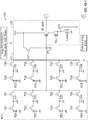
- FIG. 1A illustrates an embodiment of a shared-pixels architecture 100 for use as a pixel of a pixel readout system, in accordance with an exemplary embodiment.
- the image sensor can be a solid-state image sensor, for example a CMOS image sensor, which has four four-transistor (4T) pixels sharing pixel circuitry and a compact layout.
- the 4T 4-shared-pixels architecture 100 can be used as the pixel architecture for pixels in the pixel array, in some embodiments.
- the 4T 4-shared-pixels architecture 100 includes four pixels, and though many such similar shared-pixels architectures exist and may be arranged in the array in a similar manner, for simplicity only one 4T 4-shared-pixels architecture 100 is shown in greater detail.
- the 4T 4-shared-pixels architecture 100 includes four photodiode circuits in parallel.
- the photo diode circuits comprise photodiodes PD1-PD4 and their corresponding transfer gates TG1-TG4.
- Each of the photodiode circuits also comprises a timing circuit TS1-TS4 and a storage capacitor CS1-CS4 in series with the respective photodiodes PD1-PD4 between the photodiodes PD1-PD4 and a floating diffusion node.
- the individual storage capacitors CS1-CS4 for each of the photodiodes PD1-PD4 may be used to temporarily store charge absorbed by each of the photodiodes PD1-PD4 before the charge is transferred to the floating diffusion node.
- the pixel readout system may comprise a floating diffusion node FD, reset transistor RST, voltage supply VDD, source follower amplifier SF_AMP, selector transistor SEL, output voltage node Vcol, and current source Ibias. These elements can perform similar functions as described above. Sharing of the floating diffusion node FD, source follower amplifier SF_AMP, row select transistor SEL, and reset transistor RST between adjacent photodiodes PD1-PD4 and transfer gates TG1-TG4 assists in increasing the fill factor of the pixel architecture, the fill factor representing the percentage of the pixel area that is sensitive to light.
- the fill factor is increased because the sharing of components between multiple pixel architectures reduces the total number of transistors, capacitors, and other components, coupled to a larger number of shared-pixels in the shared-pixels architecture 100.
- the sharing of components among a plurality of pixels reduces the area of the pixel filled with transistors and other components, and thus increases the area of the pixel that is sensitive to light.
- the illustrated architecture 100 results in approximately 2.0 transistors per pixel.
- Components can be shared by four separate photodiodes and associated transfer gates. In some embodiments, the shared components may be shared by eight separate photodiodes or 16 separate photodiodes or more separate photodiodes.
- photodiodes PD1-PD4 can include one photodiode used to detect a red component of incoming light, two photodiodes used to detect a green component of incoming light, and one photodiode used to detect a blue component of incoming light.
- the color representation described may follow the Bayer color pattern, wherein a shared architecture comprises two green pixels in diagonal and one red pixel in diagonal with one blue pixel in a four-pixel architecture.
- the floating diffusion node FD of Figure 1A may represent one or more floating diffusion nodes.
- each photodiode circuit may have an individual floating diffusion node (not shown in this figure).
- two or more photodiode circuits may share one or more floating diffusion nodes (not shown in this figure). However, as depicted herein, the one or more floating diffusion nodes may be combined into a single floating diffusion node FD in the figures for simplicity of the schematics.
- Charge can be collected by each of the photodiodes PD1-PD4 as long as the corresponding transfer gates TG1-TG4 are off.
- the accumulated charges in each of the photodiodes PD1-PD4 may be temporarily transferred to the respective storage capacitors CS1-CS4.
- the charge that accumulates in photodiode PD1 when the transfer gate TG1 is closed and the photodiode is exposed to light of the specified color may be transferred to the storage capacitor CS1 when the transfer gate TG1 is opened.
- the transfer gates TG1-TG4 may be closed.
- the storage capacitors CS1-CS4 may have larger charge capacities than the photodiodes PD1-PD4, and the storage capacitors CS1-CS4 may receive multiple charge dumps from their respective photodiodes PD1-PD4 before the charges in the storage capacitors CS1-CS4 are transferred to the floating diffusion node FD. The charges may be further transferred to the floating diffusion node FD when the respective timing circuits TS1-TS4 are activated while the transfer gates TG1-TG4 are closed.
- both the transfer gates TG1-TG4 and the timing circuits TS1-TS4 may be open at the same time, thus allowing both the accumulated charges in the photodiodes PD1-PD4 and the charges in the storage capacitors CS1-CS4 to accumulate in the floating diffusion node FD.
- the individual storage capacitors CS1-CS4 and timing circuits TS1-TS4 allow charges from the corresponding photodiodes PD1-PD4 to be transferred to the floating diffusion node FD individually.
- the intermediate storage of charge in the storage capacitors CS1-CS4 between the photodiodes PD1-PD4 and the floating diffusion node FD may be useful in discerning charge contributions from individual photodiodes PD1-PD4. Without the individual storage capacitors CS1-CS4, in some embodiments, a single, shared storage capacitor or floating diffusion node FD may have difficulty supporting multiple charge transfers from multiple photodiodes PD1-PD4 without losing signal and creating artifacts.
- the floating diffusion node FD which may comprise a parasitic capacitor inside the silicon wafer of the photodiodes PD1-PD4, may not hold enough charge for extending the dynamic range of a sensor with small pixels. Accordingly, the charge from the photodiodes PD1-PD4 can be dumped multiple times to their respective storage capacitors CS1-CS4 before the charges from each of the storage capacitors CS1-CS4 are readout individually through the floating diffusion node FD to the readout circuitry described above.
- the storage capacitors CS1-CS4 can be configured with an effective capacitance large enough to store multiple charge dumps from their respective photodiodes PD1-PD4, for example eight or more charge dumps.
- the full well capacity of a pixel can be effectively multiplied in the analog domain by the number of charge dumps stored in the storage capacitors CS1-CS4.
- the storage capacitors CS1-CS4 and the timing circuits TS1-TS4 are formed on the same layer as the photodiodes PD1-PD4 in the shared-pixels architecture 100.
- the storage capacitors CS1-CS4 and the timing circuits TS1-TS4 may be formed on the second layer, along with the remaining components of the readout circuitry.
- the corresponding one or more photodiodes PD1-PD4, the one or more storage capacitors CS1-CS4, and the floating diffusion node FD can be reset, dependent upon which TG1-TG4 and TS1-TS4 are activated.
- the photodiodes PD1-PD4 and the storage capacitors CS1-CS4 may each be reset before being exposed to the light source. Charge integration in the photodiodes PD1-PD4 can occur when the respective transfer gates TG1-TG4 are off, allowing photon charge to be collected in the corresponding photodiode PD1-PD4.
- Charge integration in the storage capacitors CS1-CS4 can occur when the respective timing circuits TS1-TS4 are off and the respective transfer gates TG1-TG4 are open to allow charge from the photodiodes PD1-PD4 to accumulate in the storage capacitors CS1-CS4.
- charge integration in the photodiodes PD1-PD4 can occur when the respective transfer gates TG1-TG4, timing circuits TS1-TS4, and reset transistor RST are all off, allowing photon charge to be collected in the corresponding photodiode PD1-PD4.
- the transfer gate TG1-TG4 By selectively turning on the transfer gate TG1-TG4, the charge in the corresponding photodiode PD1-PD4 (for example, the one or more photodiodes PD1-PD4 having an associated transfer gate turned on) is transferred to the floating diffusion node FD via the storage capacitors CS1-CS4 and the timing circuits TS1-TS4.
- one or more transfer gates TG1-TG4 and the timing circuits TS1-TS4 can be turned on simultaneously to transfer charge directly from associated photodiodes PD1-PD4 directly to the floating diffusion node FD without storing it in the storage capacitors CS1-CS4.
- the charge stored in the floating diffusion node FD is converted to a voltage through the amplifier SF_AMP. This readout voltage may be transferred on the Vcol output.
- the charge stored in one of the storage capacitors CS1-CS4 can be converted to a voltage through the amplifier SF_AMP when the respective timing circuits TS1-TS4 are turned on, and this readout voltage may be transferred on the Vcol output.
- the charged stored in one of the photodiodes PD1-PD4 can be converted to a voltage through the amplifier SF_AMP when the respective transfer gates TG1-TG4 and timing circuits TS1-TS4 are turned on.
- the timing circuits TS1-TS4 can include high-speed logic for regulating the number of charge dumps sent from the photodiodes PD1-PD4 to the storage capacitors CS1-CS4 and for determining when to open to allow the charge in the respective storage capacitors CS1-CS4 to be readout via the floating diffusion node. In some embodiments, only one storage capacitor of the storage capacitors CS1-CS4 may be readout by the readout circuitry at one time. Thus, the timing circuits TS1-TS4 may be coordinated so that no two are open together.
- Sequential readout of photodiodes PD1-PD4 using the timing circuits TS1-TS4 and the readout circuitry can control the readout of photodiodes PD1-PD4 to increase resolution in comparison to parallel scanning.
- the timing scheme can be a transistor with a line width of approximately 20 nm.
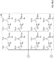
- FIG. 1B illustrates an embodiment of an interlaced four transistor 4-shared-pixels architecture, generally designated as a first architecture 105, in accordance with an exemplary embodiment.
- a first architecture 105 there are four photodiodes PDR1, PDR2, PDG1, and PDG3 (or similar structures or devices), with one pair of photodiodes for a first color, for example red (PDR1 and PDR2), and a second pair of the photodiodes for a second color, for example green (PDG1 and PDG3).
- These photodiodes PDR1, PDR2, PDG1, and PDG3 may correspond to the photodiodes PD1-PD4 as referenced in Figure 1A .
- each of the photodiodes PDR1, PDR2, PDG1, and PDG3 have a dedicated transfer gate TG1-TG4 to control the integration time of charges at each of the respective photodiodes PDR1, PDR2, PDG1, and PDG3.
- transfer gate TG1 controls the integration and transfer of charge in the photodiode PDR1
- the transfer gate TG2 controls the integration and transfer of charge in the photodiode PDR2.
- transfer gates TG3 and TG4 of Figure 1B control the integration and transfer of charge in photodiodes PDG1 and PDG3, respectively.
- the three transistors shown between the pairs of photodiodes PDR1-PDR2 and PDG1-PDG3 are shared between the four photodiodes PDR1, PDR2, PDG1, and PDG3.
- the transistor at the top of this column of transistors is the amplifying transistor SF_AMP, the middle transistor is the selection transistor SEL, and the bottom transistor is the reset transistor RST.
- Two floating diffusion nodes FD1 and FD2 are shown, FD1 being located between the photodiodes PDR1 and PDG1 and the amplifying transistor SF_AMP and FD2 being located between the photodiodes PDR2 and PDG3 and the amplifying transistor SF_AMP.
- the two floating diffusion nodes FD1 and FD2 may be combined into a single floating diffusion node or split into additional floating diffusion nodes. Not shown in the shared pixel circuitry is the timing circuitry TS and the storage capacitor CS, though in some embodiments, these two components may be included in the shared pixel circuitry.
- the photodiodes PDR1 and PDR2 are the two photodiodes in the left-most column of the schematic of Figure 1B .
- the photodiodes PDR1 and PDR2 are configured to sense red light.
- the photodiodes PDR1 and PDR2 each generate a charge in response to the amount of red light sensed over a period of time.
- the photodiodes PDG1 and PDG3 are the two photodiodes in the right-most column and are each configured to sense green light, each generating a charge when green light is sensed.
- the center column comprises the shared transistors SF_AMP, SEL, and RST and the shared floating diffusion points FD1 and FD2.
- the SF_AMP may be configured to convert the charge input from one of the photodiodes PDR1, PDR2, PDG1, and PDG3 into corresponding voltage signals to be output during a readout sequence.
- the selection transistor SEL may be configured to select a single row of the pixel array to be readout (or output), as described above and may allow the amplifying transistor SF_AMP to convert a charge to a voltage when a given row or column is selected.
- the reset transistor RST may be configured to clear (or set to a reference point) the charge of each the photodiodes PDR1, PDR2, PDG1, and PDG3 and floating diffusion nodes FD1 and FD2. To reset the photodiodes PDR1, PDR2, PDG1, and PDG3, the reset transistor RST may need to be turned on in conjunction with the transfer gates TG1, TG2, TG3, and TG3, respectively.
- Figure 1C illustrates an embodiment of two four transistor 4-shared-pixels architecture of Figure 1B in an interlaced pixel architecture array, in accordance with an exemplary embodiment.
- a first four transistor 4-shared-pixels architecture may correspond to the first architecture 105 from Figure 1B .
- a second four transistor 4-shared-pixels architecture may be depicted as a second architecture 110.
- the first four transistor 4-shared-pixels architecture 105 on the left comprises photodiodes PDR1, PDR2, PDG1, and PDG3 along with transistors SF_AMP, SEL, and RST and floating diffusion nodes FD1 and FD2.
- the second four transistor 4-shared-pixels architecture 110 on the right comprises photodiodes PDB1, PDB2, PDG2, and PDG4 along with transistors SF_AMP1, SEL1, and RST1 and floating diffusion nodes FD3 and FD4.
- the components of the second four transistor 4-shared-pixels architecture 110 function the same as the components described above in relation to Figures 1A and 1B , with the photodiodes PDB1 and PDB2 being configured to generate a current in response to sensed blue light.
- PDG2 and PDG4 of the second four transistor 4-shared-pixels architecture generate current signals in response to exposure to green light in addition to those generated by PDG1 and PDG3.
- Floating diffusion node FD3 may be located between the photodiodes PDB1 and PDG1 and the amplifying transistor SF AMP1 and FD4 may be located between the photodiodes PDB2 and PDG4 and the amplifying transistor SF_AMP 1.
- the combination of the two four transistor 4-shared-pixels architectures 105 and 110 may provide a color representation following the Bayer color pattern, where every full unit comprises two green pixels (for example, one green-odd pixel and one green-even pixel) in diagonal paired with the blue pixel and the red pixel in diagonal.
- PDG1 and PDG3 may be referred to as green-odd photodiodes while PDG2 and PDG4 may be referred to as green-even photodiodes.
- other color patterns may be used in an interlaced array; the selection between the various color patterns may be dependent at least upon an application of the pixel array.
- the shared components in the center column of the second architecture 110 comprise the transistors SF_AMP1, SEL1, and RST1 and the floating diffusion points FD3 and FD4.
- the SF_AMP1, as described above, may be configured to convert the charge input from one of the photodiodes PDB1, PDB2, PDG2, and PDG4 into corresponding voltage signals to be readout.
- the selection transistor SEL2 may be configured to select a single row of the second architecture 110 pixel array to be readout (or output), as described above.
- the reset transistor RST1 may be configured to clear the charge of each photodiodes PDB1, PDB2, PDG2, and PDG4 and floating diffusion nodes FD3 and FD4.
- the respective transfer gates TG1_1, TG2_1, TG3_1, and TG4_1 may be activated in conjunction with the reset transistor RST1.
- Figure 2 depicts the four transistor 4-shared-pixels architectures 105 and 110 of Figures 1B and 1C in an interlaced pixel architecture array designated interlaced array 200, in accordance with an exemplary embodiment.
- Figure 2 may depict how the interlaced architectures 105 and 110 of Figures 1B and 1C may line up physically.
- the four transistor 4-shared-pixels architectures 105 and 110 of Figure 1C are shown forming the interlaced array 200 of six four transistor 4-shared-pixels architectures (three each of both 105 and 110).
- the first row of 4-shared-pixels architectures may be pixel architectures 105
- the second row of 4-shared-pixels architectures may be pixel architectures 110.
- each of the six four transistor, 4-shared-pixels architectures comprises the components described above in relation to Figures 1B and 1C (e.g., each comprises four photodiodes (not labeled individually in this figure), four transfer gate transistors (not labeled individually in this figure), and shared reset, selection, and amplifying transistors (not labeled individually in this figure)).
- the transfer gate transistors and the reset and selection transistors of each four transistor 4-shared-pixels architecture are further coupled to the buses indicated on the left side of Figure 2 .
- the embodiment illustrated in Figure 2 depicts twelve buses associated with six signals, each of the six signals being communicated on two separate buses.
- the two separate buses for each signal may be used to communicate with the separate shared-pixels architectures due to the interlaced layout in the array, wherein the photodiodes and transistors of adjacent pixel architectures forming the interlaced array 200 are not all aligned in a single horizontal direction.
- the transistors for each 4-shared-pixels architecture 105 may not be in a single row horizontally across the array, and are instead separated into alternating rows of red and green-even photodiodes PDRm and PDGn, where m represents the number of the photodiode PDX being depicted and n represents the number of the photodiode PDX being depicted, respectively, and blue and green-odd photodiodes PDBm and PDGn, respectively.
- the TG1_m transistors of two adjacent 4-shared-pixels architectures 105 and 110 may not be in a single row, but rather in two rows offset from each other.
- the transfer gates of Figures 1B and 1C above are coupled to the TG_1 and TG_2 bus lines of Figure 2 , respectively.
- the transfer gates of Figures 1B and 1C above are coupled to the TG_3 and TG_4 bus lines of Figure 2 , respectively.
- the reset transistors of the four transistor 4-shared-pixels architectures 105 and 110 of Figure 2 are each coupled to the reset bus line RST.
- the select transistors of the four transistor 4-shared-pixels architectures 105 and 110 of Figure 2 are each coupled to the selection bus line SEL.
- the amplifying transistors and the selection transistors are each further coupled to one of the vertical channels indicated on the top and bottom of Figure 2 .
- the Figure 2 depicts readout channels that readout a voltage corresponding to the charge stored in the photodiodes.
- the readout channels alternate in upward/downward vertical directions, wherein each of the photodiodes of a given four transistor 4-shared-pixels architecture 105 and 110 are connected to a single channel.
- shared architecture 105 is connected to the readout channel 205, while the shared architecture 110 is coupled to the readout channel 210.
- the readout channel 205 comprises pbus_yl and pvh_yl, wherein the voltage from pbus_yl is transferred to pvh_yl via the selection transistor and the amplifying transistor based on the charge within the photodiode being readout when the row selection transistor is active and the transfer gate transistor is active for the particular photodiode.
- These readout channels may each be coupled to the amplifying and selection shared transistors of the shared-pixels architectures such that the charges of the photodiodes of the shared-pixels architectures 105 and 110 across the interlaced array 200 are output via the readout channels 205 and 210.
- each pair of readout channels may be configured to output signals from two columns of shared-pixels architectures 105 and 110 of the interlaced array 200.
- Each of the readout signal channels of the pair of readout channels described above may be dedicated to a specific pair of colors.
- the pvh_y1/pbus_y1 readout channel may be dedicated to reading-out signals from the red photodiodes and the green-even photodiodes
- the readout channel pvh_y2/pbus_y2 may be dedicated to reading-out signals from the blue photodiodes and the green-odd photodiodes.
- the readout channels may be disposed along the interlaced array 200 such that the readout channel/photodiode color correlation is maintained.
- each readout channel of the pair of readout channels may be configured to readout according to a timing scheme, alternating between the two photodiode colors of the coupled shared-pixels architecture 105 or 110, such that a single color is readout on the channel at a particular moment.
- a timing scheme is described in further detail below in reference to Figures 3A , 3B , 6A , and 6B .
- each photodiode of each shared-pixels architecture 105 and 110 may generate a charge when exposed to their respective colors of light. However, while the respective transfer gate associated with the photodiode generating the charge is closed, the charge is not transferred away from the photodiode. For example, when photodiode PD1 of Figure 1A is exposed to red light, the photodiode PD1 may generate a charge. While transfer gate TG1 is closed, the charge is not transferred away from the photodiode PD1 and is instead integrated (e.g., accumulates) in the photodiode PD1.
- transfer gate TG1 When the transfer gate TG1 receives a signal on the TG_1 bus, transfer gate TG1 may open, allowing the charge from the photodiode PD1 to transfer to the floating diffusion node FD1.
- the floating diffusion node FD1 may store the charge received from the PD1 over time.
- the floating diffusion node FD1 may be reset if the reset transistor RST receives a reset signal from the RST bus, or may alternatively output the integrated charge via the amplifying transistor SF_AMP in response to the selection transistor SEL receiving a selection signal from the SEL bus.
- the floating diffusion node FD1 may transfer the charge stored therein to a storage capacitor CS1.
- the amplifying transistor SF_AMP may convert the integrated charge to be output on the readout channel pvh_y1/pbus_y1. This process may be similarly applied to each photodiode PD of the shared-pixels architecture 105 and 110 such that the readout channel may be dedicated to a single color at any given moment.
- the shared-pixels architecture 105 and 110 depicted in Figures 1B-2 may provide various advantages with respect to the depicted layout and architecture.
- the vertical readout channels may provide a 1-color-per-channel readout when the readouts are performed according to a timing scheme.
- a 1-color-per-channel readout each color has a dedicated channel at a given point in time.
- the first four-shared-pixels architecture may comprise red photodiodes PDR1 and PDR2 with green odd photodiodes PDG1 and PDG3.
- the vertical readout channel 205 may be dedicated to a single color when paired with a timing scheme that alternates between reading out the red photodiodes PDR1 and PDR2 and the green odd photodiodes PDG1 and PDG3.
- the green odd and red colors have a dedicated channel when being readout. The same applies for the green even and blue photodiodes PDG2, PDG4, PDB1, and PDB2.
- the one color-per-channel readout made available by the integrated 4-shared-pixels architecture 105 and 110 may have advantages of its own, including the ability to deliver signals with lower noise and higher gain than the signals delivered by channels shared by more than one color. This may result from each channel being fully separate from the other channels, allowing changes for one signal to be kept independent from the other signals. Additionally, the one color-per-channel may provide a lower fixed-pattern noise than embodiments where multiple colors share a channel, because the photodiodes are not combined in a single channel, and offset and gain error corrections may be applied color-independent. Furthermore, the one color-per-channel readout may result in shared row control and smaller areas for the shared-pixels architecture 105 and 110 and thus the interlaced array 200.
- the separate channels per color may also provide for parallel processing capabilities, such that high resolution devices (for example, HD cameras and digital SLR cameras) are able to process the high resolutions at a high data rate. Additionally, temporal noise may be reduced by the separate channels because smaller capacitors (e.g., storage capacitors) may be used, which contribute to the temporal noise.
- high resolution devices for example, HD cameras and digital SLR cameras
- digital SLR cameras digital SLR cameras
- temporal noise may be reduced by the separate channels because smaller capacitors (e.g., storage capacitors) may be used, which contribute to the temporal noise.
- Table 1 below compares the interlaced shared-pixels architecture disclosed herein with non-interlaced shared-pixels architectures.
- TABLE 1 Avg. H line / pix Avg. V line / pix V binning Output / col. Readout ckt / col. 1 ch per color 2x2 shared 3 1 No 0.5 1 No 2x2 tg shared 2 1 No 0.5 1 No 4x1 shared 1.5 2 Yes 1 1 1 No I4shared 3 2 Yes 1 2 Yes I4tgshard 2 2 Yes 1 2 Yes
- a 2x2 shared-pixels architecture may provide an average of 3 horizontal lines per pixel, one average vertical line per pixel, no vertical binning, 0.5 outputs colors per column, one readout circuit per column, and no single channel per color capability.
- a 2x2 transfer gate shared-pixels architecture may provide an average of 2 horizontal lines per pixel, one average vertical line per pixel, no vertical binning, 0.5 outputs colors per column, one readout circuit per column, and no single channel per color capability.
- a 4x1 shared-pixels architecture may provide an average of 1.5 horizontal lines per pixel, 2 average vertical lines per pixel, vertical binning, 1 output color per column, one readout circuit per column, and no single channel per color capability.
- An integrated shared-pixels architecture may provide an average of 3 horizontal lines per pixel, 2 average vertical lines per pixel, vertical binning, 1 output color per column, 2 readout circuits per column, and single channel per color capability.
- An integrated transfer gate shared-pixels architecture may provide an average of 2 horizontal lines per pixel, 2 average vertical lines per pixel, vertical binning, 1 output color per column, 2 readout circuits per column, and single channel per color capability.
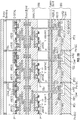
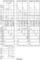
- Figure 3A illustrates a 4 color-per-channel readout sequence of a 1x4 interlaced 4-shared-pixels architecture, in accordance with an exemplary embodiment.
- Figure 3A depicts an example of an array of red, blue, and green pixels in a Bayer configuration.
- Each of the pixels in the array may be referenced according to their respective row and column number, [r,c], where 'r' represents the row number and 'c' represents the column number.
- pixel [0,0] may correspond to the Gr pixel in the top-left corner of the array, where the top row is row 0 and the left-most column is column 0.
- Each column and row of pixels of the array comprises two colors of pixels in an alternating fashion.
- each pixel is coupled to a vertical readout channel of the plurality of vertical readout channels 305 (upward) and 310 (downward).
- the vertical readout channels 305a-305c may correspond to the vertical readout channels 205, while the vertical readout channel 310a-310c may correspond to the vertical readout channels 210, as referenced in Figure 2 .
- the green Gr and green Gb pixels are coupled to the same downward readout channels 310a-310c, while the red R and blue B pixels are coupled to the same upward readout channels 305a-305c.
- On the left side of the pixel array are shown representative signals TG_1, TG_2, TG_3, and TG_4, each corresponding to one of the rows 0, 1, 2, and 3, respectively.
- the signals TG_1, TG_2, TG_3, and TG_4 may correspond to the signals received on the buses of the same designation as referenced in Figure 2 . Accordingly, when the TG_1 bus indicates a signal to the TG1 transfer gates, the pixels of the row to which the TG1 transfer gates are connected (here, row 0) are readout vertically.
- the diagram shows how the charges from the colored pixels are readout of the shared-pixels architecture and "dumped" into sample-and-hold capacitors in parallel and later shifted out sequentially based on the selection signal SEL (not shown in this figure) and the transfer gate signals TG_1-TG_4.
- each color is readout as a separate color channel when readout according to a timing scheme, thus allowing each color channel to have a different gain applied to it to reach a desired color fidelity and/or white balance (e.g., different color processing per channel is available, as discussed above).
- the TG_1 signal is received by the respective transfer gate TG1, the pixels in row 0 may be readout on their corresponding readout channels 305 and 310.
- a readout of the pixels in row 0 may result in Gr pixel [0,0] being readout by downward readout channel 310a, R pixel [0,1] being readout by upward readout channel 305b, Gr pixel [0,2] being readout by downward readout channel 310b, R pixel [0,3] being readout by upward readout channel 305c, and Gr pixel [0,4] being readout by downward readout channel 310c.
- the remaining rows 1-3 may be readout into the sample-and-hold capacitors.
- each readout channel 305a-305c and 310a-310c may feed into a separate sample-and-hold capacitor.
- the sample-and-hold capacitors may be shared between two or more readout channels 305a-305c and 310a-310c.
- the diagram further shows the sequence of channel readouts separated by corresponding row numbers, referred to as banks 306 and 311.
- the first upward readout channel 305a collects charges from the blue pixels of column 0, as shown by the first column of readout charges ⁇ discard, B[1,0], discard, B[3,0] ⁇ .
- the "discard" charges are charges that are ignored because there is no pixel to be readout.
- the row 0 readout for upward readout channel 305a may be discarded because there is no column of pixels to the left of the upward readout channel 305a, so the upward readout channel 305a reads out a value that does not correspond to a charge of an existing pixel. Accordingly, values that are readout that do not correspond to charges from existing pixels may be simply discarded or ignored.
- Charges B[1,0] and B[3,0] represent the charges from the two blue pixels in column 0 in rows 1 and 3, respectively.
- upward readout channel 305b reads out charged ⁇ R[0,1], B[1,2], R[2,1], B[3,2] ⁇ , gathering the red and blue charges from both columns 1 and 2, and upward readout channel 305c gathers the red and blue charges from both columns 3 and 4, resulting in ⁇ R[0,3], B[1,4], R[2,3], B[3,4] ⁇ .
- the sequence of channel readouts separated by corresponding row numbers indicates what pixel was readout in by a particular channel.
- readout channel 305a had a discarded charge value
- readout channel 305b had a charge from the red pixel at [0,1]
- readout channel 305c had the charge from the red pixel at [0,3]
- readout channel 305d (not shown in this figure) had the charge from the red pixel at [0,5].
- the sequence of channel readouts for the remaining rows 1-3 for the upward readout channels 305a-305d and the rows 0-3 for the downward readout channels 310a-310c depict charge sources in a similar fashion.
- the sequence of channel readouts for downward readout channels 310a-310c may be shown in bank 311.
- the charges in the pixels may be readout in parallel across each column, as each column for a given row only receives a charge from a single color pixel to be stored in the respective sample-and-hold capacitors. Subsequently, the charges in the sample-and-hold capacitors are shifted out sequentially.
- the data have to be aligned correctly, or readout according to a given pattern or time sequence.
- the odd-numbered rows of bank 306 may be delayed by one "horizontal" clock (e.g., one pixel time), while the even and odd rows of bank 311 may also be delayed by one "horizontal” clock.
- the vertical sharing as shown in Figure 3A is similar to the traditional vertical shared interlaced pixels architecture. Additionally, the shared architecture is capable of charge binning in both the horizontal and vertical directions. Charge binning may be important because it allows the charge in more than one pixel/photodiode to be combined in either or both of the horizontal and vertical directions in the analog domain. This charge binning may thus boost the charge capacity (e.g., the total available charge) that may be saved from the photodiodes. Pixel level binning made available by the interlaced shared-pixels architecture may provide for better low-light performance, where capturing and displaying full resolution of an image may be difficult. Charge binning may boost the output level by combining the outputs of horizontal and vertical pixels.
- charge capacity e.g., the total available charge
- each four transistor four-shared-pixels architecture 105 and 110 may be combined into a single pixel output when combined with proper timing schemes (e.g., horizontal binning) and then combined vertically with outputs from other four transistor four-shared-pixels architectures (e.g., vertical binning).
- proper timing schemes e.g., horizontal binning
- vertically with outputs from other four transistor four-shared-pixels architectures e.g., vertical binning
- Such binning may be useful in "preview modes" as provided in various imaging devices, where, because previous modes tend to display an image at a reduced resolution, the preview mode generated by an array of interlaced shared-pixels architectures may be of a higher resolution than those generated by non-interlaced shared-pixels architectures.
- Figure 3B illustrates a 4 color-per-channel readout sequence of a 2x2 interlaced 4-shared-pixels architecture, in accordance with an exemplary embodiment.
- Figure 3B depicts an example of an array of red, blue, and green pixels in a Bayer configuration.
- Each of the pixels in the array may be referenced according to their respective row and column number, [r,c], where 'r' represents the row number and 'c' represents the column number.
- pixel [0,0] may correspond to the Gr pixel in the top-left corner of the array, where the top row is row 0 and the left-most column is column 0.
- Each pixel may be coupled to a vertical readout channel of the plurality of vertical readout channels 355 (upward) and 360 (downward).
- the vertical readout channels may correspond to the vertical readout channels 205 and 210 as referenced in Figure 2 .
- the green Gr and red R pixels are coupled to the same upward readout channels 355a-355d, while the green Gb and blue B pixels are coupled to the same downward readout channels 360a-360c.
- On the left side of the pixel array are shown representative signals TG_1, TG_2, TG_3, and TG_4, each corresponding to one of the rows 0, 1, 2, and 3, respectively.
- the signals TG_1, TG 2, TG 3, and TG 4 may correspond to the signals received on the buses of the same designation as referenced in Figure 2 . Accordingly, when the TG_1 bus indicates a signal to the TG1 transfer gates, the pixels of the row to which the TG1 transfer gates are connected (here, row 0) are readout vertically.
- the diagram shows how the charges from the colored pixels are readout of the shared-pixels architecture and "dumped" into sample-and-hold capacitors in parallel and later shifted out sequentially based on the selection signal SEL (not shown in this figure) and the transfer gate signals TG_1-TG_4, according to a timing scheme (not shown in this figure).
- the TG_1 signal is received by the respective transfer gate TG1, the pixels in row 0 may be readout on their corresponding readout channels 355 and 360.
- a readout of the pixels in row 0 may result in Gr pixel [0,0] being readout by upward readout channel 355a, R pixel [0,1] being readout by upward readout channel 355b, Gr pixel [0,2] being readout by upward readout channel 355b, R pixel [0,3] being readout by upward readout channel 355c, and Gr pixel [0,4] being readout by upward readout channel 355c.
- the remaining rows 1-3 may be readout into the upward and downward sample-and-hold capacitors.
- each readout channel 355a-355d and 360a-360c may feed into a separate sample-and-hold capacitor.
- the sample-and-hold capacitors may be shared between two or more readout channels 355a-355d and 360a-360c. Accordingly, in the 2x2 interlaced 4-shared-pixels structure, each row of pixels is read out on alternating readout channels. The single channel per color may be maintained by reading out specific colored pixels and specific times, such that only red pixels may be read out vertically at a given time, while green Gr pixels are readout vertically on the same channel at a different time.
- the diagram further shows the sequence of channel readouts separated by corresponding row numbers, referred to as banks 356 and 361.
- the first upward readout channel 355a collects charges from the green Gr pixels of column 0, as shown by the first column of readout charges ⁇ discard, Gr[0,0], discard, Gr[2,0] ⁇ .
- the "discard" charges are charges that are ignored because there is no pixel to be readout.
- the row 0 readout for upward readout channel 305a may be discarded because there is no column of pixels to the left of the upward readout channel 305a, so the upward readout channel 305a reads out a value that does not correspond to a charge of an existing pixel. Accordingly, values that are readout that do not correspond to charges from existing pixels may be simply discarded or ignored.
- Charges Gr[0,0] and Gr[2,0] represent the charges from the two green Gr pixels in column 0 in rows 0 and 2, respectively.
- upward readout channel 305b reads out charges ⁇ R[0,1], Gr[0,2], R[2,1], Gr[2,2] ⁇ , gathering the red and green Gr charges from both columns 1 and 2, and upward readout channel 305c gathers the red and green Gr charges from both columns 3 and 4, resulting in ⁇ R[0,3], Gr[0,4], R[2,3], Gr[2,4] ⁇ .
- the sequence of channel readouts separated by corresponding row numbers indicates what pixel(s) was readout by a particular channel.
- readout channel 305a had a discarded charge value
- readout channel 305b had a charge from the red pixel at [0,1]
- readout channel 305c had the charge from the red pixel at [0,3]
- readout channel 305d (not shown in this figure) had the charge from the red pixel at [0,5].
- the sequence of channel readouts for the remaining rows 1-3 for the upward readout channels 305a-305d and the rows 0-3 for the downward readout channels 310a-310c depict charge sources in a similar fashion.
- the sequence of channel readouts for downward readout channels 310a-310c may be shown in bank 361.
- the charges in the pixels may be readout in parallel across each column, as each column for a given row receives a charge from two color pixels to be stored in the respective sample-and-hold capacitors. Subsequently, the charges in the sample-and-hold capacitors are shifted out sequentially.
- the data have to be aligned correctly, or readout according to a given pattern or time sequence. For example, the odd-numbered rows of bank 356 may be delayed by one "horizontal" clock, while the even and odd rows of bank 361 may also be delayed by one "horizontal” clock.
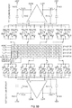
- Figure 4A illustrates an embodiment of an interlaced four transistor 8-shared image sensor pixels architecture 400 having a pixel readout system, in accordance with an exemplary embodiment.
- the image sensor can be a solid-state image sensor, for example a CMOS image sensor, which has eight four transistor (4T) pixels sharing pixel circuitry and a compact layout.
- the 4T 8-shared-pixels architecture 400 can be used as the pixel architecture for pixels in the pixel array, in some embodiments.
- the 4T 8-shared-pixels architecture 400 includes eight pixels, and though many such pixels may be arranged in the array, for simplicity only one 4T 8-shared-pixels architecture 400 is shown in greater detail.
- the 4T 8-shared-pixels architecture 400 includes eight photodiode circuits, a floating diffusion node FD, a reset transistor RST, a voltage supply VDD, a source follower amplifier SF_AMP, a selector transistor SEL, an output voltage node Vcol, and a current source Ibias.
- the photodiode circuits may each comprise a photodiode PD1-PD8, a transfer gate TG1-TG8, a storage capacitor CS1-CS8, and a timing circuit TS1-TS8.
- the floating diffusion node FD may represent one or more floating diffusion points dedicated to one photodiode circuit or shared between multiple photodiode circuits.
- the readout circuitry components depicted in Figure 4A can perform similar functions as described above with respect to Figures 1A-2 . These components can be shared by the eight separate photodiode circuits having their associated photodiodes PD1-PD8, transfer gates TG1-TG8, storage capacitors CS1-CS8, and timing circuits TS1-TS8. Sharing of the floating diffusion node FD, source follower amplifier SF_AMP, row select transistor SEL, and reset transistor RST between adjacent photodiode circuits (for example, in series) assists in increasing the fill factor of the pixel architecture, the fill factor representing the percentage of the pixel area that is sensitive to light.
- the illustrated architecture 400 results in approximately 1.5 transistors per pixel.
- two photodiodes may be used to detect a red component of incoming light, four photodiodes may be used to detect a green component of incoming light, and two photodiodes may be used to detect a blue component of incoming light, in accordance with a Bayer color pattern.
- the timing circuits TS1-TS8 of the photodiode circuits can include high-speed logic for regulating the number of charge dumps sent from the photodiodes PD1-PD8 to the storage capacitors CS1-CS8 and for determining when to open to allow the charge in the respective storage capacitors CS1-CS8 to be readout via the floating diffusion node.
- only one storage capacitor of the storage capacitors CS1-CS8 may be readout by the readout circuitry at one time.
- the timing circuits TS1-TS8 may be coordinated so that no two are open together.
- the accumulated charge can be read out from the storage capacitors CS1-CS8 through the floating diffusion node FD, through the source follower SF_AMP, and through the select transistor SEL to the output voltage node Vcol.
- Figure 4A also illustrates one embodiment of partitioning of the pixel array and pixel circuitry into separate, stacked structures (e.g., silicon wafers).
- a stacked structure may be desired where the number of components and general layout of the shared-pixels architecture limits the area available for light absorption.
- all of the components depicted may be placed on the same layer (for example, the same piece of silicon).
- the limited area may be easily filled by the shared components and individual photodiodes PD, transfer gates TG, storage capacitors CS, and timing circuits TS.
- the large number of components reduces the amount of light capable of being absorbed by the photodiodes PD because some of the light may reflect off of or be blocked by these components and structures coupling the components in the area of the photodiode PD. Additionally, as more components (e.g., transistor, contacts, or buses) are introduced into the shared-pixels interlaced array architecture co-planar with the photodiodes PD, less space may be available and more light may be blocked from reaching the photodiodes PD where stacking is not utilized.
- more components e.g., transistor, contacts, or buses
- the components of the shared pixels architecture may be separated onto different layers in a stacked pixel structure.
- a first portion including the photodiodes PD1-PD8, the corresponding transfer gates TG1-TG8, the corresponding storage capacitors CS1-CS8, the corresponding timing circuits TS1-TS8, and the floating diffusion node FD can be placed in a photodiode wafer 410 configured to integrate charge from incoming light.
- a second portion including the reset transistor RST, the voltage supply VDD, the source follower amplifier SF_AMP, the selector transistor SEL, the output voltage node Vcol, and the current source Ibias can be placed in a pixel circuitry wafer 420.
- the pixel circuitry wafer 420 may be constructed on top of the photodiode wafer 410 opposite the side exposed to incoming light. Accordingly, the surface space for detecting the incoming light can be increased through both the space-saving design of the shared-pixels architecture as well as the separation of the photodiodes and the pixel circuitry into different wafers.
- the pixel circuitry components and structures are located on an individual layer (e.g., the pixel circuitry wafer 420), more real estate is made available for absorbing the incoming light on the photodiode wafer 410.
- connection points between the bottom and top layers may be the floating diffusion nodes.
- the timing circuitry TS and source follower amplifier SF_AMP of the pixel circuitry wafer 420 can be connected to the floating diffusion node FD of the photodiode wafer.
- the connection points may be the row/column interconnections.
- the separation or partitioning of the shared architecture into the three-dimensional stack configuration is not a trivial matter.
- the relocation of components between the various layers may be limited by current technology (for example, the determination between fusion bonds or fine-pitch hybrid bonds, as will be discussed below), and the partitioning and locating of the various components may impact the performance of the shared-pixels architecture. For example, the signal-to-noise ratio, the charge capacity, or how well the background noise may be suppressed may each be impacted by the partitioning of the components between the various 3-D layers.
- the photodiode wafer 410 may be configured as a back side illuminated (BSI) image sensor, wherein the photodiodes PD1-PD8, transfer gates TG1-TG8, the storage capacitors CS1-CS8, and the timing circuits TS1-TS8 described above are integrated into the BSI image sensor.
- the BSI image sensor may have a structure attached thereto to provide support for the BSI image sensor, which may have a lower structural integrity due to manufacturing and design constraints (e.g., due to the BSI image sensor having to be very thin to allow for light to penetrate to the silicon substrate, the BSI image sensor wafer may be fragile and susceptible to damage).
- the structure supporting the BSI image sensor wafer may be a "dummy" or “blank” silicon wafer; accordingly, the components placed in the pixel circuitry wafer 420 may be integrated into the support wafer used to provide structural support for the BSI image sensor.
- the BSI image sensor may be designed to be more sensitive to light, wherein the electrical components used to generate and readout signals in response to sensed light may be more efficiently located structurally.
- the components as indicated as being on the photodiode wafer 410 or the pixel circuitry wafer 420 may be manipulated or changed such that different components are on different wafers than as shown in Figure 4A .
- components of the shared-pixels architecture may be separated between the photodiode wafer 410 and the pixel circuitry wafer 420 based on having similar electrical characteristics, manufacturing techniques, operational restrictions, or any other characteristic that may affect the design, manufacture, or operation of the imaging sensor being designed or the components integrated into the imaging sensor.
- various other 3D stacked designs or technologies may be implemented and may partition circuit components, elements, and blocks by ways of various stacked technologies and characteristics (for example, pad pitch or density). Such designs and implementations may deliver superior detector performance which 2D sensor configurations may not fulfill.
- the components integrated into the upper layer may be connected with the components integrated into the lower layer (e.g., the photodiode wafer 410) via a connection at one or more connection points.
- the floating diffusion node FD may be configured to function as the connection point between the upper layer (the pixel circuitry layer 420) and the lower layer (the photodiode wafer 410) via a fine-pitch hybrid bond.
- the floating diffusion nodes may be configured to function as the connection point between the upper layer and the lower layer via a fusion bond.
- the reset transistor RST and source follower amplifier SF_AMP of the pixel circuitry wafer 420 can be connected to the floating diffusion node FD of the photodiode wafer 410. More details regarding the fine-pitch hybrid bonds will be provided below in relation to Figure 5A , while additional details regarding the fusion bonds will be provided in relation to Figure 5B . Various other types of bonds may be utilized to couple the upper and lower layers of wafers.
- Figure 4B and Figure 4C illustrate two sections of an embodiment of a four transistor 16-shared image sensor pixel architecture 450 having a pixel readout system, in accordance with an exemplary embodiment, wherein connection points A-B indicate continuation of elements between the Figures 4B and 4C .
- Some embodiments of the image sensor can be a solid-state image sensor, for example a CMOS image sensor, which has sixteen 4T pixels sharing pixel circuitry and a compact layout.
- the 4T 16-shared-pixels architecture 450 can be used as the pixel architecture for pixels in the pixel array.
- the 4T 16-shared-pixels architecture 450 includes sixteen pixels, and though many such pixels are arranged in the array, for simplicity only one 4T 16-shared-pixels architecture 450 is shown in greater detail.
- the 4T 16-shared-pixels architecture 450 includes sixteen photodiodes circuits, a floating diffusion node FD, a reset transistor RST, a voltage supply VDD, a source follower amplifier SF_AMP, a selector transistor SEL, an output voltage node Vcol, and a current source Ibias.
- the floating diffusion node FD may represent one or more floating diffusion points dedicated to one photodiode circuit or shared between multiple photodiode circuits.
- the components of Figures 4B and 4C can perform similar functions as described above with respect to Figures 1A and 4A .
- the components of the readout circuitry can be shared by sixteen separate photodiode circuits.
- the photodiode circuits may comprise the photodiodes PD1-PD16, the transfer gates TG1-TG16, the storage capacitors CS1-CS16, and the timing circuits TS1-TS16. Sharing of the floating diffusion node FD, the source follower amplifier SF_AMP, the row select transistor SEL, and the reset transistor RST between adjacent photodiode circuits may assist in increasing the fill factor of the pixel architecture, the fill factor representing the percentage of the pixel area that is sensitive to light.
- the illustrated architecture 450 results in approximately 1.25 transistors per pixel.
- the photodiodes PD1-PD16 may be used to detect a red component of incoming light, eight photodiodes may be used to detect a green component of incoming light, and four photodiodes may be used to detect a blue component of incoming light.
- the timing circuits TS1-TS16 of the photodiode circuits can include high-speed logic for regulating the number of charge dumps sent from the photodiodes PD1-PD16 to the storage capacitors CS1-CS16 and for determining when to open to allow the charge in the respective storage capacitors CS1-CS16 to be readout via the floating diffusion node.
- only one storage capacitor of the storage capacitors CS1-CS16 may be readout by the readout circuitry at one time.
- the timing circuits TS1-TS16 may be coordinated so that no two are open together.
- the accumulated charge can be read out from the storage capacitors CS1-CS16 through the floating diffusion node FD, through the source follower SF_AMP, and through the select transistor SEL to the output voltage node Vcol.
- Figures 4B and 4C also illustrate one embodiment of partitioning of the pixel array and pixel circuitry into separate, stacked structures (e.g., silicon wafers), similar to that described above in relation to Figure 4A .
- a first portion including the photodiodes PD1-PD16, the corresponding transfer gates TG1-TG16, the corresponding storage capacitors CS1-CS16, the corresponding timing circuits TS1-TS16, and the floating diffusion node FD can be placed in a photodiode wafer 460 configured to integrate charge from incoming light.
- a second portion including the reset transistor RST, the voltage supply VDD, the source follower amplifier SF_AMP, the selector transistor SEL, the output voltage node Vcol, and the current source Ibias can be placed in a pixel circuitry wafer 470.
- one or more of these components may be placed in a third pixel circuitry wafer, not shown in this figure. Accordingly, the surface space for detecting light can be increased through both the space-saving design of the shared-pixels architecture as well as the separation of the photodiode circuits and the pixel circuitry into different wafers.
- the surface space for detecting light may be increased because when the pixel circuitry structures and components forming the same are located on the same layer as the photodiode circuits, e.g., the photodiode wafer 460, the available real estate for absorbing light is reduced (for example, the light is reflected or blocked by the components or the connections there between and thus not absorbed by the photodiodes PD1-PD16).
- the photodiode wafer 460 may be configured as a back side illuminated (BSI) image sensor, wherein the components described above as being placed in the photodiode wafer 460 are integrated into the BSI image sensor.
- BSI back side illuminated
- a BSI image sensor may have a structure attached thereto to provide support for the BSI image sensor, which may have a lower structural integrity due to manufacturing and design constraints (e.g., due to the BSI image sensor having to be very thin to allow for light to penetrate to the silicon substrate, the BSI image sensor wafer may be fragile and susceptible to damage).
- this structure supporting the BSI image sensor wafer may be a "dummy" or "blank” silicon wafer; accordingly, the components placed in the pixel circuitry wafer 470 may be integrated into the support wafer used to provide structural support for the BSI image sensor.
- the BSI image sensor may be designed to be more sensitive to light, wherein the electrical components used to generate and readout signals in response to sensed light may be more efficiently located structurally in a manner that increases the area with which the photodiode PD may absorb light.
- the components as indicated as being on the photodiode wafer 460 or the pixel circuitry wafer 470 may be manipulated or changed such that different components are on different wafers than as shown in Figures 4B and 4C .
- components of the shared-pixels architecture may be separated between the photodiode wafer 460 and the pixel circuitry wafer 470 based on having similar electrical characteristics, manufacturing techniques, operational restrictions, or any other characteristic that may affect the design, manufacture, or operation of the imaging sensor being designed or the components integrated into the imaging sensor.
- the components integrated into the upper layer may be connected with the components integrated into the lower layer (e.g., the photodiode wafer 460) via a connection at one or more connection points.
- the floating diffusion node FD may be configured to function as the connection point between the upper layer (the pixel circuitry layer 470) and the lower layer (the photodiode wafer 460) via a fine-pitch hybrid bond.
- the upper and lower layers may be connected via a fusion bond at the same or a different connection point than the floating diffusion node FD.
- the fusion bond may be used for row or column interconnections, wherein the readout of a full row or column is transferred to the upper layer.
- the type of bonds between the upper and lower layers may determine, in part, the division of components between the upper layer and the lower layer. For example, when fusion bonds are used to couple the upper and lower layer, more of the components may be integrated into the lower layer.
- the selection transistor SEL and source follower amplifier SF_AMP of the pixel circuitry wafer 470 can be connected to the floating diffusion node FD of the photodiode wafer 460. More details regarding the fine-pitch hybrid bonds will be provided below in relation to Figure 5A , while additional details regarding the fusion bonds will be provided in relation to Figure 5B .
- the photodiode wafer 460 may comprise a detector array wafer and the pixel circuitry wafer may comprise a Pixel FET/AFE/ADC Mixed-Mode ASIC Wafer, as shown in Figures 4B and 4C .
- Figure 5A illustrates an embodiment of a 3D stacked CMOS image sensor comprising the interlaced shared-pixels architecture of Figures 4A , 4B , and 4C with pixel level fine-pitch hybrid bonding.
- the 3D stacked CMOS image sensor depicts three distinct layers of the 3D stacked CMOS image sensor.
- the first (bottom) layer 505 may comprise the lower layer described above as being the photodiode wafer 410, 460.
- the first layer 505 may comprise a BSI sensor layer.
- the BSI sensor layer 505 as shown illustrates a sample of three photodiodes PD1-PD3 from the shared-pixels architectures of Figures 1A-1C .
- the photodiodes PD1-PD3 are shown having the transfer gates TG1-TG3, respectively, connecting the photodiodes PD1-PD3 to individual floating diffusion nodes FD1-FD3.
- the floating diffusion nodes FD1-FD3 are shown as each connecting to the middle layer 506 via individual fine-pitch hybrid bonds.
- the second (middle) layer 506 may comprise the upper layer described above as being the pixel circuitry wafer 470.
- the second layer 506 may comprise the analog front end (AFE), A/D conversion circuitry, and the pixel circuitry described above.
- the second layer 506 may comprise the reset transistor RST, the selection transistor SEL, the amplifying transistor SF_AMP, and the timing circuit TS with the storage capacitor CS.
- the second layer 506 may previously comprised the supporting wafer that provided structural support for the BSI sensor layers but did not provide any functional capabilities.
- the second layer 506 may be configured to provide structural support and functional support via the pixel circuitry components integrated into the second layer 506.
- the third (top) layer 507 may be configured as the image signal processor or digital signal processing layer or readout circuitry layer.
- the third layer 507 may comprise the logic chips or other circuitry configured to perform final processing and/or reading out of the signals generated by the BSI sensor and converted to digital form by the readout circuitry.
- the third layer 507 may be excluded from the CMOS 3D stacked structure, and the components configured to further process the signal from the pixel circuitry may be integrated into the second layer 506.
- an incoming light 510 to which the photodiodes PD1-PD3 are exposed may emit upward from the bottom of the figure, thereby allowing the majority of light generated to be incident on the photodiodes PD1-PD3 without having to pass through the pixel circuitry wafer 470.
- the relocation of the components for the pixel circuitry to the second layer 506 clears area on the first layer 505 that may not provide more exposure of the photodiodes PD1-PD3 to the light.
- the photodiodes PD1-PD3 may be more efficient, faster, Based on the light to which they are exposed, the photodiodes PD1-PD3 may generate current signals that may be transferred to the floating diffusion nodes when the respective transfer gate TG1-TG3 are activated via a signal from the transfer gate buses (not shown in this figure). Then the current signals in the floating diffusion nodes FD1-FD3 may be transferred to the pixel circuitry of the second layer 506 via the fine-pitch hybrid bonds. The pixel circuitry may then configure the current signals received via the fine-pitch hybrid bonds to be readout at 1-color per channel as described above in relation to Figures 2 and 3 .
- Figure 5B illustrates another embodiment of a 3D stacked CMOS image sensor comprising the interlaced shared-pixels architecture of Figures 4A and 4B with column/row level fusion bonding.
- the first (bottom) level 555 is identified as being the BSI sensor layer
- the second level 556 is identified as the analog front end (AFE) and analog digital conversion (ADC) layer
- the third level 557 is identified as being the ISP/DSP
- the fourth (top) layer is the PC board substrate (PCB), for example F/R4.
- the structure and integrated components of the various layers may be similar to those of the layers 505-507 of Figure 5A .
- the structure and integrated components of the various layers may be different than those of the layers 505-507 of Figure 5A . While the division of components between the first layer 505 and the second layer 506 of Figure 5A corresponded to the division of components as shown in Figures 4A and 4B , the division of components between the first layer 555 and the second layer 556 of Figure 5B may correspond to a division where the majority of the components of the photodiode circuit and the pixel circuit are on the same layer.
- Figures 4A and 4B depict the photodiodes PD1-PD3 and transfer gates TG1-TG3 as being on a detector array wafer 410, 460 while the shared pixel circuitry was separated on the pixel circuitry wafer 420, 470
- the 3D cross-section shown in Figure 5B represents a layout where all of the components of Figures 4A and 4B are integrated onto the same layer of silicon except for the current source Ibias and wherein the bottom layer is coupled to the middle layer via one or more fusion bonds.
- the photodiodes PD1-PD3 may be configured to convert light energy received via the light 560 flowing upward from the bottom of the page to current signals.
- the converted current signals may be transferred from the photodiodes PD1-PD3 to the floating diffusion nodes FD1-FD3 associated with each of the photodiodes PD1-PD3 via transfer gate transistors TG1-TG3 in response to receiving signal on the respective buses TG_1-TG_3 as referenced in Figures 4A and 4B .
- the second layer 556 may comprise an analog layer.
- the second layer 556 may comprise the analog front end (AFE) and A/D conversion circuitry described above.
- the second layer 556 may comprise the components configured to perform analog manipulation of the signals received from the BSI sensor layer (first layer 555).
- the second layer 556 may previously comprised the supporting wafer that provided structural support for the BSI sensor layers but did not provide any functional capabilities.
- the second layer 556 may be configured to provide structural support and functional support via the analog components integrated into the second layer 556.
- the readout circuitry components may be integrated into the second layer 556. This circuitry may include the sample/hold capacitors discussed above and other components used to readout the charge values from the pixels.
- the third layer 557 may be configured as the image signal processor or digital signal processing layer or readout circuitry layer.
- the third layer 557 may comprise the logic chips or other circuitry configured to perform final processing and/or reading out of the signals generated by the BSI sensor and converted to digital form by the readout circuitry.
- the third layer 557 may be excluded from the CMOS 3D stacked structure, and the components configured to further process the signal from the readout circuitry may be integrated into the third layer 557.
- Figure 6A and Figure 6B illustrate two sections of a timing diagram of the interlaced four transistor 4-shared image sensor pixel architecture of Figure 1B , in accordance with one exemplary embodiment, having connection points A-X to indicate continuation of elements between Figures 6A and 6B .
- Figures 6A and 6B show a timing diagram with time increasing along the x-axis and with the on-off activations of various signals along the y-axis.
- the various signals along the y-axis may correspond to transistors or other components of the pixel circuit described above or the readout circuit described above.
- the top half of the timing diagram shows activation timings for the Reset transistor (referred to as RES in Figures 1A-2 ; labeled “Reset” in Figures 6A and 6B ), the transfer gates (referred to as TG1-TG4 in Figures 1A-2 ; labeled TG_P1, TG_P2, TG_P3, TG_P4 in Figures 6A and 6B ), and timing for the activation of the row selection transistor (referred to as SEL in Figures 1A-2 ; labeled Row_Sel in Figures 6A and 6B ).
- the bottom half of the timing diagram shows activation timings for components feeding various sample/hold capacitors (labeled SM11, SM21, SM12, and SM22 in Figures 6A and 6B ) and column amplifying switches (labeled Phi21 and Phi22 in Figures 6A and 6B ).
- the activation timings of the transistors and other components are shown in conjunction with the activation timings of the sample and hold components SM11, SM21, SM12, and SM22 and column amplifying components Phi21 and Phi22.
- the timing diagram illustrates that the Reset transistor is activated periodically.
- the photodiodes referred to as PD1-PD4 in Figures 1A-2 ; labeled P1-P4 in Figures 6A and 6B ) are Reset to a default voltage to which the Reset transistor is coupled.
- the Reset transistor and the transfer gate TG_P1 are shown as both being activated at the same time.
- the photodiode coupled to the TG_P1 transfer gate e.g., photodiode PD1
- the transfer gates TG_P1-TG_P4 are activated simultaneously with the reset transistor at different times, such that only a single transfer gate TG_P1-TG_P4 is activated concurrently with the reset transistor.
- the reset transistor Reset is active but none of the transfer gates TG_P1-TG_P4 is active, the storage capacitor or the floating diffusion node is reset to the coupled voltage.
- the time period between activations for a transfer gate TG_P1-TG_P4 associated with a photodiode PD may represent the integration period of the photodiode coupled to the particular TG_P1-TG_P4.
- the photodiode coupled to the transfer gate TG_P1 e.g., PD1
- the photodiode coupled to the transfer gate TG_P1 may integrate light and generate a charge corresponding to the integrated light.
- the photodiode PD1 may be reset when both the transfer gate transistor TG_P1 and the reset transistor Reset are activated at the same time.
- the accumulated charge at PD1 may be transferred to a storage capacitor/floating diffusion node.
- each of the transfer gates TG_P1-TG_P4 have an integration time associated with them between subsequent activations of the respective transfer gates TG_P1-TG_P4.
- the row selection transistor Row_Sel indicates when the row selection transistor is activated for a readout of a particular transfer gate TG_P1-TG_P4 and photodiode combination.
- the photodiodes may integrate the light until the transfer gate TG_P1-TG_P4 associated with the photodiode is activated to transfer the integrated charge to the storage capacitor.
- a "one row time” may indicate the amount of time that passes during which a single row of pixels is readout.
- the readout of a row may comprise reading-out more than one pixel.
- each of the four rows shown may comprise two different pixels.
- the amount of time that passes between the beginning of a first P1 readout and a second, subsequent P1 readout may be defined as the "one frame time," wherein the pixels of a given frame are each readout.
- the 't_pix" time shown on the timing diagram may indicate the pixel time, which completed a sampling of the reset and signal levels of one single pixel during the readout period. When reading out all the pixels in a row, the time period is referred to as one row time.
- the row selection transistor Row Sel performs two readouts for each photodiode PD1-PD4.
- the two separate readouts of each photodiode PD1-PD4 may provide for compensation and/or reduction of noise.
- the row selection transistor Row_Sel is activated for a first readout of the storage capacitor and/or floating diffusion node. This initial readout occurs shortly after the storage capacitor and/or floating diffusion node is reset by the reset transistor Reset activating at time t4; this initial readout may provide the baseline for the noise associated with the readout.
- the transfer gate TG_P1 may be activated at time t6 to transfer the charge from the photodiode PD 1 coupled to the transfer gate transistor TG_P1 to the storage capacitor and/or floating diffusion node. Then, after TG_P1 is activated at time t6, the row selection transistor Row_Sel is activated at time t7 for a second readout of the storage capacitor and/or floating diffusion node. This second readout may provide a readout value that may be corrected based on the baseline readout value. The two readouts indicated may correspond to the noise reduction measures described above.
- the readout column circuitry may comprise a sample/hold capacitor per column.
- the readout column circuitry for an imaging system may comprise a pair of sample/hold capacitors per column. In either case, the sample/hold capacitor(s) may be used to reduce a noise readout of the imaging system, as described above.
- the signals SM11, SM21, SM12, and SM22 may represent the signals used to obtain the baseline (reference) and the readout (sample).
- the SM11 sample/hold: reset signal may be used to obtain the baseline of the storage capacitor or floating diffusion node prior to the "dumping" of the charge from one of the photodiodes PD1-PD4 into the storage capacitor or floating diffusion node, as shown at time t5.
- the SM21 sample/hold signal may be used to obtain the charge transferred from the photodiode P1.
- the charge read at time t5 may be subtracted from the charge read at time t7 to obtain the readout value without the noise that is common between the baseline and the sampled values.
- the column-ampSW-1/SW-2 may represent the amplifying components that are amplifying the readout values from the top and bottom column readout channels, as depicted in Figure 7 .
- Figure 7 illustrates an example of a readout block diagram of the interlaced four transistor 4-shared image sensor pixel architecture of Figure 1B according to the timing diagram of Figures 6A and 6B .
- the various components above and below the pixel array comprise the sampling switches, the sampling capacitors, the column addressing multiplexors and signal and reset buses, and the variable gain amplifier. These components, in combination, may receive signals from the pixel array, amplify the signals and multiplex the signals out to one or more video signals.
- Figure 8 illustrates a high-level schematic diagram of an embodiment of an image capture device 700, the device 700 having a set of components including an image processor 720 linked to a camera 701 (image sensor).
- the image processor 720 is also in communication with a working memory 765, memory 730, and device processor 755, which in turn is in communication with storage 770 and an optional electronic display 760.
- Device 700 may be a portable personal computing device, e.g. a mobile phone, digital camera, tablet computer, personal digital assistant, or the like. Device 700 may also be a stationary computing device or any device. A plurality of applications may be available to the user on device 700. These applications may include traditional photographic and video applications, for example applications relating to user management of number of charge dumps, number of differential frames, HDR imaging applications, and the like.
- the image capture device 700 includes camera 701 for capturing external images.
- the camera 701 can include a pixel array 710 and readout circuitry with additional storage capacitor 715 as described above.
- the storage capacitors can have the capacitance to store a number of charge dumps from the associated pixel.
- the camera 701 can be configured for continuous or intermittent capture of preview frames, as well as capture of full resolution final images.
- the image processor 720 may be configured to perform various processing operations on received preview frames.
- Processor 720 may be a general purpose processing unit or a processor specially designed for imaging applications. Examples of image processing operations include AWB and AEC data generation, LED current calculation, cropping, scaling (e.g., to a different resolution), image stitching, image format conversion, color interpolation, color processing, image filtering (e.g., spatial image filtering), lens artifact or defect correction, etc.
- Processor 720 may, in some embodiments, comprise a plurality of processors.
- Processor 720 may be one or more dedicated image signal processors (ISPs) or a software implementation of a processor.
- ISPs dedicated image signal processors
- the image processor 720 is connected to a memory 730 and a working memory 765.
- the memory 730 stores capture control module 735, full well capacity extension module 740, noise compensation module 780, and operating system 750.
- the modules of the memory 730 include instructions that configure the image processor 720 of device processor 755 to perform various image processing and device management tasks.
- Working memory 765 may be used by image processor 720 to store a working set of processor instructions contained in the modules of memory 730. Alternatively, working memory 765 may also be used by image processor 720 to store dynamic data created during the operation of device 700.
- Full well capacity extension module 740 can store sub-modules timing scheme module 742 and charge dump number handler module 744. Together, these modules can cooperate to perform the tasks relating to determining each pixel's integration time and multiple charge dumps from the pixel to the storage capacitor in the readout architecture.
- Noise compensation module 780 can store sub-modules frame capture module 782 and digital aggregation module 784.
- frame capture module 782 can be provided with instructions that configure the processor 720 to perform the process 500 described above by providing instructions to the readout circuitry of the image sensor.
- digital aggregation module 784 can be provided with instructions that configure the processor 720 to perform the process 600 described above to aggregate multiple charges in the digital domain.
- the image processor 720 is configured by several modules stored in the memories.
- the capture control module 735 may include instructions that configure the image processor 720 to adjust the focus position of camera 701.
- Capture control module 735 may further include instructions that control the overall image capture functions of the device 700.
- capture control module 735 may include instructions that call subroutines to configure the image processor 720 to capture preview image data or full resolution image data including one or more frames of a target image scene using the camera 701.
- Operating system module 750 configures the image processor 720 to manage the working memory 765 and the processing resources of device 700.
- operating system module 750 may include device drivers to manage hardware resources for example the camera 701. Therefore, in some embodiments, instructions contained in the image processing modules discussed above may not interact with these hardware resources directly, but instead interact through standard subroutines or APIs located in operating system component 750. Instructions within operating system 750 may then interact directly with these hardware components. Operating system module 750 may further configure the image processor 720 to share information with device processor 755.
- Device processor 755 may be configured to control the display 760 to display the captured image, or a preview of the captured image, to a user.
- the display 760 may be external to the imaging device 200 or may be part of the imaging device 200.
- the display 760 may also be configured to provide a view finder displaying a preview image for a use prior to capturing an image, for example present the user with a visual representation of the dynamic range of the image scene or with a user interface for manually adjusting the number of analog charge dumps and/or digitally accumulated differential frames.
- the display 760 may comprise an LCD or LED screen, and may implement touch sensitive technologies.
- Device processor 755 may write data to storage module 770, for example data representing digitally accumulated differential frames. While storage module 770 is represented graphically as a traditional disk device, those with skill in the art would understand that the storage module 770 may be configured as any storage media device.
- the storage module 770 may include a disk drive, e.g. a floppy disk drive, hard disk drive, optical disk drive or magneto-optical disk drive, or a solid state memory e.g. a FLASH memory, RAM, ROM, and/or EEPROM.
- the storage module 770 can also include multiple memory units, and any one of the memory units may be configured to be within the image capture device 700, or may be external to the image capture device 700.
- the storage module 770 may include a ROM memory containing system program instructions stored within the image capture device 700.
- the storage module 770 may also include memory cards or high speed memories configured to store captured images which may be removable from the camera.
- the storage module 770 can also be external to device 700, and in one example device 700 may wirelessly transmit data to the storage module 770, for example over a network connection.
- Figure 8 depicts a device having separate components to include a processor, imaging sensor, and memory
- processor imaging sensor
- memory memory components
- the memory components may be combined with processor components, for example to save cost and/or to improve performance.
- Figure 8 illustrates two memory components, including memory component 720 comprising several modules and a separate memory 765 comprising a working memory
- memory component 720 comprising several modules
- a separate memory 765 comprising a working memory
- a design may utilize ROM or static RAM memory for the storage of processor instructions implementing the modules contained in memory 730.
- the processor instructions may be loaded into RAM to facilitate execution by the image processor 720.
- working memory 765 may comprise RAM memory, with instructions loaded into working memory 765 before execution by the processor 720.
- Implementations disclosed herein provide systems, methods and apparatus for increasing light absorption by photodiode pixels and enabling low-noise and high gain readouts, high resolution and high color-fidelity outputs, and increased dynamic range using 3-dimensional (3D) stacked, vertically integrated pixel architectures.
- 3D 3-dimensional
- the circuits, processes, and systems discussed above may be utilized in a wireless communication device.
- the wireless communication device may be a kind of electronic device used to wirelessly communicate with other electronic devices. Examples of wireless communication devices include cellular telephones, smart phones, Personal Digital Assistants (PDAs), e-readers, gaming systems, music players, netbooks, wireless modems, laptop computers, tablet devices, etc.
- the wireless communication device may include one or more image sensors, two or more image signal processors, a memory including instructions or modules for carrying out the CNR process discussed above.
- the device may also have data, a processor loading instructions and/or data from memory, one or more communication interfaces, one or more input devices, one or more output devices for example a display device and a power source/interface.
- the wireless communication device may additionally include a transmitter and a receiver.
- the transmitter and receiver may be jointly referred to as a transceiver.
- the transceiver may be coupled to one or more antennas for transmitting and/or receiving wireless signals.
- the wireless communication device may wirelessly connect to another electronic device (e.g., base station).
- a wireless communication device may alternatively be referred to as a mobile device, a mobile station, a subscriber station, a user equipment (UE), a remote station, an access terminal, a mobile terminal, a terminal, a user terminal, a subscriber unit, etc.
- Examples of wireless communication devices include laptop or desktop computers, cellular phones, smart phones, wireless modems, e-readers, tablet devices, gaming systems, etc.
- Wireless communication devices may operate in accordance with one or more industry standards for example the 3rd Generation Partnership Project (3GPP).
- 3GPP 3rd Generation Partnership Project
- the general term "wireless communication device” may include wireless communication devices described with varying nomenclatures according to industry standards (e.g., access terminal, user equipment (UE), remote terminal, etc.).
- Disk and disc includes compact disc (CD), laser disc, optical disc, digital versatile disc (DVD), floppy disk and Blu-ray® disc where disks usually reproduce data magnetically, while discs reproduce data optically with lasers.
- a computer-readable medium may be tangible and non-transitory.
- computer-program product refers to a computing device or processor in combination with code or instructions (e.g., a "program”) that may be executed, processed or computed by the computing device or processor.
- code may refer to software, instructions, code or data that is/are executable by a computing device or processor.
- Software or instructions may also be transmitted over a transmission medium.
- a transmission medium For example, if the software is transmitted from a website, server, or other remote source using a coaxial cable, fiber optic cable, twisted pair, digital subscriber line (DSL), or wireless technologies for example infrared, radio, and microwave, then the coaxial cable, fiber optic cable, twisted pair, DSL, or wireless technologies for example infrared, radio, and microwave are included in the definition of transmission medium.
- DSL digital subscriber line
- the methods disclosed herein comprise one or more steps or actions for achieving the described method.
- the method steps and/or actions may be interchanged with one another without departing from the scope of the claims.
- the order and/or use of specific steps and/or actions may be modified without departing from the scope of the claims.
- Couple may indicate either an indirect connection or a direct connection.
- first component may be either indirectly connected to the second component or directly connected to the second component.
- plurality denotes two or more. For example, a plurality of components indicates two or more components.
- determining encompasses a wide variety of actions and, therefore, “determining” can include calculating, computing, processing, deriving, investigating, looking up (e.g., looking up in a table, a database or another data structure), ascertaining and the like. Also, “determining” can include receiving (e.g., receiving information), accessing (e.g., accessing data in a memory) and the like. Also, “determining” can include resolving, selecting, choosing, establishing and the like.
- examples may be described as a process, which is depicted as a flowchart, a flow diagram, a finite state diagram, a structure diagram, or a block diagram.
- a flowchart may describe the operations as a sequential process, many of the operations can be performed in parallel, or concurrently, and the process can be repeated. In addition, the order of the operations may be re-arranged.
- a process is terminated when its operations are completed.
- a process may correspond to a method, a function, a procedure, a subroutine, a subprogram, etc.
- a process corresponds to a software function
- its termination corresponds to a return of the function to the calling function or the main function.
Landscapes
- Engineering & Computer Science (AREA)
- Multimedia (AREA)
- Signal Processing (AREA)
- Physics & Mathematics (AREA)
- Spectroscopy & Molecular Physics (AREA)
- Solid State Image Pick-Up Elements (AREA)
- Transforming Light Signals Into Electric Signals (AREA)
- Metal-Oxide And Bipolar Metal-Oxide Semiconductor Integrated Circuits (AREA)
Applications Claiming Priority (2)
| Application Number | Priority Date | Filing Date | Title |
|---|---|---|---|
| US14/561,845 US9774801B2 (en) | 2014-12-05 | 2014-12-05 | Solid state image sensor with enhanced charge capacity and dynamic range |
| PCT/US2015/059732 WO2016089551A1 (en) | 2014-12-05 | 2015-11-09 | Solid state image sensor with enhanced charge capacity and dynamic range |
Publications (2)
| Publication Number | Publication Date |
|---|---|
| EP3228077A1 EP3228077A1 (en) | 2017-10-11 |
| EP3228077B1 true EP3228077B1 (en) | 2021-07-14 |
Family
ID=54704089
Family Applications (1)
| Application Number | Title | Priority Date | Filing Date |
|---|---|---|---|
| EP15801029.8A Active EP3228077B1 (en) | 2014-12-05 | 2015-11-09 | Solid state image sensor with enhanced charge capacity and dynamic range |
Country Status (8)
Families Citing this family (58)
| Publication number | Priority date | Publication date | Assignee | Title |
|---|---|---|---|---|
| JP2016005068A (ja) * | 2014-06-16 | 2016-01-12 | ソニー株式会社 | 固体撮像装置および電子機器 |
| JP2016178408A (ja) * | 2015-03-19 | 2016-10-06 | キヤノン株式会社 | 固体撮像装置及びその駆動方法、並びに撮像システム |
| TWI738569B (zh) | 2015-07-07 | 2021-09-01 | 日商半導體能源研究所股份有限公司 | 成像裝置及其運作方法 |
| US10090344B2 (en) * | 2015-09-07 | 2018-10-02 | Semiconductor Energy Laboratory Co., Ltd. | Imaging device, method for operating the same, module, and electronic device |
| US10896923B2 (en) | 2015-09-18 | 2021-01-19 | Semiconductor Energy Laboratory Co., Ltd. | Method of operating an imaging device with global shutter system |
| US10109667B2 (en) | 2015-10-09 | 2018-10-23 | Semiconductor Energy Laboratory Co., Ltd. | Imaging device, module, and electronic device |
| EP3382375B1 (en) * | 2015-11-18 | 2021-05-26 | Nikon Corporation | Imaging capture element, measurement device, and measurement method |
| JP6668728B2 (ja) | 2015-12-14 | 2020-03-18 | 株式会社リコー | 光電変換素子、画像読取装置及び画像形成装置 |
| JP6732468B2 (ja) * | 2016-02-16 | 2020-07-29 | キヤノン株式会社 | 光電変換装置及びその駆動方法 |
| KR102521342B1 (ko) * | 2016-05-31 | 2023-04-14 | 에스케이하이닉스 주식회사 | 3층 적층 이미지 센서 |
| CN109479107A (zh) * | 2016-05-31 | 2019-03-15 | Bae系统成像解决方案有限公司 | 适于提供额外的颜色信息的光电检测器 |
| JP6856983B2 (ja) * | 2016-06-30 | 2021-04-14 | キヤノン株式会社 | 光電変換装置及びカメラ |
| US10270997B2 (en) * | 2016-09-08 | 2019-04-23 | Gvbb Holdings S.A.R.L. | Cross pixel interconnection |
| US10531034B2 (en) | 2016-09-08 | 2020-01-07 | Grass Valley Canada | Shared photodiode reset in a 5 transistor-four shared pixel |
| US10270987B2 (en) * | 2016-09-08 | 2019-04-23 | Gvbb Holdings S.A.R.L. | System and methods for dynamic pixel management of a cross pixel interconnected CMOS image sensor |
| US10944922B2 (en) | 2016-09-08 | 2021-03-09 | Gvbb Holdings S.A.R.L | Hybrid output multiplexer for a high framerate CMOS imager |
| US11272129B2 (en) * | 2016-09-08 | 2022-03-08 | Grass Valley Canada | Imager with vertical row addressing |
| JP6661506B2 (ja) * | 2016-09-23 | 2020-03-11 | サムスン エレクトロニクス カンパニー リミテッド | 固体撮像装置 |
| WO2018062303A1 (ja) | 2016-09-29 | 2018-04-05 | 株式会社ニコン | 撮像素子および電子カメラ |
| US10187584B2 (en) * | 2016-12-20 | 2019-01-22 | Microsoft Technology Licensing, Llc | Dynamic range extension to produce high dynamic range images |
| US10362255B2 (en) * | 2017-02-09 | 2019-07-23 | Semiconductor Components Industries, Llc | Multi-conversion gain pixel configurations |
| JP6779825B2 (ja) * | 2017-03-30 | 2020-11-04 | キヤノン株式会社 | 半導体装置および機器 |
| CN107590784A (zh) * | 2017-08-29 | 2018-01-16 | 宁夏巨能机器人股份有限公司 | 一种用于3d视觉识别的抗干扰系统及其抗干扰方法 |
| KR102489832B1 (ko) | 2018-01-12 | 2023-01-18 | 삼성전자주식회사 | 이미지 센서의 픽셀 어레이 및 이를 포함하는 이미지 센서 |
| TWI820078B (zh) | 2018-01-23 | 2023-11-01 | 日商索尼半導體解決方案公司 | 固體攝像元件 |
| KR102551862B1 (ko) * | 2018-01-29 | 2023-07-06 | 에스케이하이닉스 주식회사 | 이미지 센서 |
| CN108462841A (zh) * | 2018-03-21 | 2018-08-28 | 上海晔芯电子科技有限公司 | 像素阵列及图像传感器 |
| JP6909747B2 (ja) * | 2018-03-23 | 2021-07-28 | 株式会社東芝 | 固体撮像装置 |
| KR20200019432A (ko) | 2018-08-14 | 2020-02-24 | 에스케이하이닉스 주식회사 | 픽셀 장치 및 그를 이용한 비교 장치와 씨모스 이미지 센서 |
| CN109040624B (zh) * | 2018-09-06 | 2021-01-05 | 思特威(上海)电子科技有限公司 | 像素电路及读取方法 |
| US11323643B2 (en) | 2018-09-12 | 2022-05-03 | Dolby Laboratories Licensing Corporation | CMOS sensor architecture for temporal dithered sampling |
| US10728472B2 (en) * | 2018-10-09 | 2020-07-28 | Shenzhen Goodix Technology Co., Ltd | Image sensor with dynamic charge-domain sampling |
| TWI848008B (zh) * | 2018-10-17 | 2024-07-11 | 日商索尼半導體解決方案公司 | 攝像元件及電子機器 |
| JP7329318B2 (ja) | 2018-10-25 | 2023-08-18 | ソニーグループ株式会社 | 固体撮像装置及び撮像装置 |
| US10827135B2 (en) * | 2018-11-26 | 2020-11-03 | Bae Systems Information And Electronic Systems Integration Inc. | BDI based pixel for synchronous frame-based and asynchronous event-driven readouts |
| KR102633135B1 (ko) * | 2019-01-28 | 2024-02-02 | 삼성전자주식회사 | 이미지 센서 및 그의 동작 방법 |
| WO2020160195A2 (en) | 2019-01-29 | 2020-08-06 | Gigajot Technology Inc. | Column-interleaved pixel array |
| KR102765858B1 (ko) | 2019-02-08 | 2025-02-12 | 삼성전자주식회사 | 이미지 센서 장치 |
| KR102661820B1 (ko) | 2019-02-11 | 2024-05-02 | 삼성전자주식회사 | 이미지 센서 및 그것의 구동 방법 |
| KR102695388B1 (ko) | 2019-02-12 | 2024-08-19 | 삼성전자주식회사 | 디지털 픽셀을 포함하는 이미지 센서 |
| US11482556B2 (en) * | 2019-02-15 | 2022-10-25 | Taiwan Semiconductor Manufacturing Company, Ltd. | Low-noise image sensor having stacked semiconductor substrates |
| US11201188B2 (en) * | 2019-03-07 | 2021-12-14 | Semiconductor Components Industries, Llc | Image sensors with high dynamic range and flicker mitigation |
| KR102712158B1 (ko) | 2019-04-19 | 2024-09-30 | 삼성전자주식회사 | 광 센싱 회로 및 이를 포함하는 이미지 센서 |
| CN113711585B (zh) * | 2019-05-24 | 2025-02-25 | 索尼半导体解决方案公司 | 固态摄像装置和测距装置 |
| TW202510027A (zh) * | 2019-06-26 | 2025-03-01 | 日商索尼半導體解決方案公司 | 攝像裝置 |
| KR20210002966A (ko) | 2019-07-01 | 2021-01-11 | 삼성전자주식회사 | 이미지 센서 및 그것의 구동 방법 |
| KR102786164B1 (ko) | 2019-07-08 | 2025-03-26 | 삼성전자주식회사 | 광학적 지문 인식 기반의 지문 등록 방법 및 이를 이용한 광학적 지문 인식 방법 |
| US11438486B2 (en) | 2019-08-26 | 2022-09-06 | Qualcomm Incorporated | 3D active depth sensing with laser pulse train bursts and a gated sensor |
| CN110809823B (zh) * | 2019-09-30 | 2021-10-29 | 深圳市汇顶科技股份有限公司 | 图像传感器的半导体结构、芯片及电子装置 |
| CN112770067B (zh) * | 2019-11-01 | 2025-03-11 | 格科微电子(上海)有限公司 | Cmos图像传感器读出电路及其实现方法 |
| US11082643B2 (en) * | 2019-11-20 | 2021-08-03 | Waymo Llc | Systems and methods for binning light detectors |
| JP7665301B2 (ja) | 2020-08-03 | 2025-04-21 | キヤノン株式会社 | 光電変換装置及びその製造方法と、撮像システム |
| KR20220051052A (ko) | 2020-10-16 | 2022-04-26 | 삼성전자주식회사 | 이미지 센서 |
| JP2022092503A (ja) * | 2020-12-10 | 2022-06-22 | ソニーセミコンダクタソリューションズ株式会社 | 固体撮像装置及び電子機器 |
| KR20220149243A (ko) * | 2021-04-30 | 2022-11-08 | 에스케이하이닉스 주식회사 | 이미지 센싱 장치 |
| US20240373139A1 (en) * | 2021-09-16 | 2024-11-07 | Sony Semiconductor Solutions Corporation | Image sensor for event detection |
| JP2023104261A (ja) * | 2022-01-17 | 2023-07-28 | ブリルニクス シンガポール プライベート リミテッド | 固体撮像装置、固体撮像装置の駆動方法、および電子機器 |
| EP4365561A1 (en) * | 2022-11-04 | 2024-05-08 | STMicroelectronics (Research & Development) Limited | Ambient light sensor |
Citations (1)
| Publication number | Priority date | Publication date | Assignee | Title |
|---|---|---|---|---|
| US20140320718A1 (en) * | 2013-01-31 | 2014-10-30 | Apple Inc. | Vertically Stacked Image Sensor |
Family Cites Families (36)
| Publication number | Priority date | Publication date | Assignee | Title |
|---|---|---|---|---|
| US6977684B1 (en) * | 1998-04-30 | 2005-12-20 | Canon Kabushiki Kaisha | Arrangement of circuits in pixels, each circuit shared by a plurality of pixels, in image sensing apparatus |
| JP3592106B2 (ja) * | 1998-11-27 | 2004-11-24 | キヤノン株式会社 | 固体撮像装置およびカメラ |
| US6963370B2 (en) | 2001-09-24 | 2005-11-08 | The Board Of Trustees Of The Leland Stanford Junior University | Method for improving SNR in low illumination conditions in a CMOS video sensor system using a self-resetting digital pixel |
| US7518759B2 (en) | 2003-04-22 | 2009-04-14 | Xerox Corporation | Readout system for a CMOS-based image sensor array |
| US6927432B2 (en) | 2003-08-13 | 2005-08-09 | Motorola, Inc. | Vertically integrated photosensor for CMOS imagers |
| US7456879B2 (en) | 2003-08-29 | 2008-11-25 | Aptina Imaging Corporation | Digital correlated double sampling using dual analog path |
| US7443437B2 (en) | 2003-11-26 | 2008-10-28 | Micron Technology, Inc. | Image sensor with a gated storage node linked to transfer gate |
| US7542085B2 (en) * | 2003-11-26 | 2009-06-02 | Aptina Imaging Corporation | Image sensor with a capacitive storage node linked to transfer gate |
| US20050128327A1 (en) | 2003-12-10 | 2005-06-16 | Bencuya Selim S. | Device and method for image sensing |
| JP4940667B2 (ja) * | 2005-06-02 | 2012-05-30 | ソニー株式会社 | 固体撮像素子及びその製造方法 |
| TW201101476A (en) * | 2005-06-02 | 2011-01-01 | Sony Corp | Semiconductor image sensor module and method of manufacturing the same |
| JP4752447B2 (ja) * | 2005-10-21 | 2011-08-17 | ソニー株式会社 | 固体撮像装置およびカメラ |
| US8026966B2 (en) | 2006-08-29 | 2011-09-27 | Micron Technology, Inc. | Method, apparatus and system providing a storage gate pixel with high dynamic range |
| US8049256B2 (en) * | 2006-10-05 | 2011-11-01 | Omnivision Technologies, Inc. | Active pixel sensor having a sensor wafer connected to a support circuit wafer |
| JP4341664B2 (ja) * | 2006-10-13 | 2009-10-07 | ソニー株式会社 | 固体撮像装置および撮像装置 |
| KR100828943B1 (ko) | 2006-12-19 | 2008-05-13 | (주)실리콘화일 | 3t-4s 스텝 & 리피트 단위 셀 및 상기 단위 셀을 구비한 이미지센서, 데이터 저장 장치, 반도체 공정 마스크, 반도체 웨이퍼 |
| JP2008172580A (ja) * | 2007-01-12 | 2008-07-24 | Toshiba Corp | 固体撮像素子及び固体撮像装置 |
| KR100835892B1 (ko) * | 2007-03-26 | 2008-06-09 | (주)실리콘화일 | 칩 적층 이미지센서 |
| JP5104036B2 (ja) * | 2007-05-24 | 2012-12-19 | ソニー株式会社 | 固体撮像素子とその製造方法及び撮像装置 |
| US7782383B2 (en) | 2007-06-18 | 2010-08-24 | Aptina Imaging Corporation | Noise and parasitic capacitance reduction for 1T pixel CMOS image sensors |
| KR100858033B1 (ko) | 2007-10-15 | 2008-09-10 | (주)실리콘화일 | 4t-4s 스텝 & 리피트 단위픽셀 및 상기 단위픽셀을구비하는 이미지센서 |
| US7960768B2 (en) * | 2008-01-17 | 2011-06-14 | Aptina Imaging Corporation | 3D backside illuminated image sensor with multiplexed pixel structure |
| US7538307B1 (en) | 2008-02-19 | 2009-05-26 | Teledyne Licensing Llc | Charge multiplication CMOS image sensor and method for charge multiplication |
| US7965329B2 (en) | 2008-09-09 | 2011-06-21 | Omnivision Technologies, Inc. | High gain read circuit for 3D integrated pixel |
| JP5029624B2 (ja) | 2009-01-15 | 2012-09-19 | ソニー株式会社 | 固体撮像装置及び電子機器 |
| WO2010090167A1 (ja) | 2009-02-04 | 2010-08-12 | 株式会社 Rosnes | 固体撮像装置 |
| US20110101420A1 (en) | 2009-10-31 | 2011-05-05 | Pratik Patel | Increasing full well capacity of a photodiode used in digital photography |
| JP2012048065A (ja) | 2010-08-27 | 2012-03-08 | Canon Inc | 光電変換装置、焦点検出装置、および撮像システム |
| GB2487943A (en) | 2011-02-09 | 2012-08-15 | St Microelectronics Res & Dev | A CMOS pixel sensor with local analogue storage in each pixel circuit for capturing frames in quick succession |
| US8637800B2 (en) | 2011-04-19 | 2014-01-28 | Altasens, Inc. | Image sensor with hybrid heterostructure |
| US8686342B2 (en) * | 2012-04-09 | 2014-04-01 | Omnivision Technologies, Inc. | Double-sided image sensor formed on a single semiconductor wafer die |
| US8766387B2 (en) | 2012-05-18 | 2014-07-01 | Taiwan Semiconductor Manufacturing Company, Ltd. | Vertically integrated image sensor chips and methods for forming the same |
| US9165968B2 (en) * | 2012-09-14 | 2015-10-20 | Taiwan Semiconductor Manufacturing Co., Ltd. | 3D-stacked backside illuminated image sensor and method of making the same |
| KR101402750B1 (ko) | 2012-09-26 | 2014-06-11 | (주)실리콘화일 | 3차원 구조를 가지는 이미지센서의 분리형 단위화소 |
| CN104737290B (zh) | 2012-10-26 | 2017-09-19 | 奥林巴斯株式会社 | 固体摄像装置、摄像装置以及信号读出方法 |
| US9318640B2 (en) | 2013-03-15 | 2016-04-19 | Taiwan Semiconductor Manufacturing Company, Ltd. | Method and apparatus for image sensor packaging |
-
2014
- 2014-12-05 US US14/561,845 patent/US9774801B2/en active Active
-
2015
- 2015-11-09 WO PCT/US2015/059732 patent/WO2016089551A1/en active Application Filing
- 2015-11-09 ES ES15801029T patent/ES2882168T3/es active Active
- 2015-11-09 EP EP15801029.8A patent/EP3228077B1/en active Active
- 2015-11-09 JP JP2017528895A patent/JP6408707B2/ja active Active
- 2015-11-09 CN CN201580065627.8A patent/CN107004688B/zh active Active
- 2015-11-09 CA CA2964962A patent/CA2964962C/en active Active
- 2015-11-09 KR KR1020177015090A patent/KR101853242B1/ko active Active
Patent Citations (1)
| Publication number | Priority date | Publication date | Assignee | Title |
|---|---|---|---|---|
| US20140320718A1 (en) * | 2013-01-31 | 2014-10-30 | Apple Inc. | Vertically Stacked Image Sensor |
Also Published As
| Publication number | Publication date |
|---|---|
| ES2882168T3 (es) | 2021-12-01 |
| CN107004688B (zh) | 2019-04-05 |
| CA2964962C (en) | 2018-11-06 |
| KR101853242B1 (ko) | 2018-04-27 |
| CA2964962A1 (en) | 2016-06-09 |
| JP6408707B2 (ja) | 2018-10-17 |
| BR112017011803A2 (pt) | 2017-12-26 |
| EP3228077A1 (en) | 2017-10-11 |
| CN107004688A (zh) | 2017-08-01 |
| JP2018504013A (ja) | 2018-02-08 |
| US9774801B2 (en) | 2017-09-26 |
| WO2016089551A1 (en) | 2016-06-09 |
| KR20170091619A (ko) | 2017-08-09 |
| US20160165159A1 (en) | 2016-06-09 |
Similar Documents
| Publication | Publication Date | Title |
|---|---|---|
| EP3228077B1 (en) | Solid state image sensor with enhanced charge capacity and dynamic range | |
| US9692997B2 (en) | Pixel readout architecture for full well capacity extension | |
| US10271037B2 (en) | Image sensors with hybrid three-dimensional imaging | |
| CN108200367B (zh) | 像素单元和形成像素单元的方法及数字相机成像系统组件 | |
| KR102369398B1 (ko) | 고체 촬상 장치 및 그 구동 방법, 및 전자 기기 | |
| KR102429308B1 (ko) | 고체 촬상 소자, 전자 기기, 및 촬상 방법 | |
| US9591244B2 (en) | Solid-state imaging device having plural hybrid pixels with dual storing function | |
| US20130070109A1 (en) | Imaging system with foveated imaging capabilites | |
| CN108305884A (zh) | 像素单元和形成像素单元的方法及数字相机成像系统组件 | |
| CN108282625A (zh) | 像素单元和形成像素单元的方法及数字相机成像系统组件 | |
| US10075663B2 (en) | Phase detection pixels with high speed readout | |
| CN108269819A (zh) | 像素单元和形成像素单元的方法及数字相机成像系统组件 | |
| CN108234910A (zh) | 成像系统和形成堆叠成像系统的方法及数字相机成像系统组件 | |
| US20220385852A1 (en) | Solid-state imaging device, method for driving solid-state imaging device, and electronic apparatus | |
| WO2016089548A1 (en) | Pixel readout architecture for full well capacity extension | |
| JP2015201793A (ja) | 撮像素子及び撮像装置 | |
| BR112017011803B1 (pt) | Sensor de imagem em estado sólido com capacidade de carga e faixa dinâmica melhoradas | |
| JP6733714B2 (ja) | 撮像装置 | |
| KR20160097937A (ko) | 이미지 센싱 장치 |
Legal Events
| Date | Code | Title | Description |
|---|---|---|---|
| STAA | Information on the status of an ep patent application or granted ep patent |
Free format text: STATUS: THE INTERNATIONAL PUBLICATION HAS BEEN MADE |
|
| PUAI | Public reference made under article 153(3) epc to a published international application that has entered the european phase |
Free format text: ORIGINAL CODE: 0009012 |
|
| STAA | Information on the status of an ep patent application or granted ep patent |
Free format text: STATUS: REQUEST FOR EXAMINATION WAS MADE |
|
| 17P | Request for examination filed |
Effective date: 20170411 |
|
| AK | Designated contracting states |
Kind code of ref document: A1 Designated state(s): AL AT BE BG CH CY CZ DE DK EE ES FI FR GB GR HR HU IE IS IT LI LT LU LV MC MK MT NL NO PL PT RO RS SE SI SK SM TR |
|
| AX | Request for extension of the european patent |
Extension state: BA ME |
|
| DAV | Request for validation of the european patent (deleted) | ||
| DAX | Request for extension of the european patent (deleted) | ||
| STAA | Information on the status of an ep patent application or granted ep patent |
Free format text: STATUS: EXAMINATION IS IN PROGRESS |
|
| 17Q | First examination report despatched |
Effective date: 20181002 |
|
| GRAP | Despatch of communication of intention to grant a patent |
Free format text: ORIGINAL CODE: EPIDOSNIGR1 |
|
| STAA | Information on the status of an ep patent application or granted ep patent |
Free format text: STATUS: GRANT OF PATENT IS INTENDED |
|
| RIC1 | Information provided on ipc code assigned before grant |
Ipc: H01L 27/146 20060101ALI20210120BHEP Ipc: H04N 5/3745 20110101AFI20210120BHEP Ipc: H04N 5/369 20110101ALI20210120BHEP |
|
| INTG | Intention to grant announced |
Effective date: 20210205 |
|
| GRAS | Grant fee paid |
Free format text: ORIGINAL CODE: EPIDOSNIGR3 |
|
| GRAA | (expected) grant |
Free format text: ORIGINAL CODE: 0009210 |
|
| STAA | Information on the status of an ep patent application or granted ep patent |
Free format text: STATUS: THE PATENT HAS BEEN GRANTED |
|
| AK | Designated contracting states |
Kind code of ref document: B1 Designated state(s): AL AT BE BG CH CY CZ DE DK EE ES FI FR GB GR HR HU IE IS IT LI LT LU LV MC MK MT NL NO PL PT RO RS SE SI SK SM TR |
|
| REG | Reference to a national code |
Ref country code: GB Ref legal event code: FG4D |
|
| REG | Reference to a national code |
Ref country code: IE Ref legal event code: FG4D |
|
| REG | Reference to a national code |
Ref country code: DE Ref legal event code: R096 Ref document number: 602015071335 Country of ref document: DE |
|
| REG | Reference to a national code |
Ref country code: AT Ref legal event code: REF Ref document number: 1411561 Country of ref document: AT Kind code of ref document: T Effective date: 20210815 |
|
| REG | Reference to a national code |
Ref country code: NL Ref legal event code: FP |
|
| REG | Reference to a national code |
Ref country code: SE Ref legal event code: TRGR |
|
| REG | Reference to a national code |
Ref country code: LT Ref legal event code: MG9D |
|
| REG | Reference to a national code |
Ref country code: ES Ref legal event code: FG2A Ref document number: 2882168 Country of ref document: ES Kind code of ref document: T3 Effective date: 20211201 |
|
| REG | Reference to a national code |
Ref country code: AT Ref legal event code: MK05 Ref document number: 1411561 Country of ref document: AT Kind code of ref document: T Effective date: 20210714 |
|
| PG25 | Lapsed in a contracting state [announced via postgrant information from national office to epo] |
Ref country code: HR Free format text: LAPSE BECAUSE OF FAILURE TO SUBMIT A TRANSLATION OF THE DESCRIPTION OR TO PAY THE FEE WITHIN THE PRESCRIBED TIME-LIMIT Effective date: 20210714 Ref country code: RS Free format text: LAPSE BECAUSE OF FAILURE TO SUBMIT A TRANSLATION OF THE DESCRIPTION OR TO PAY THE FEE WITHIN THE PRESCRIBED TIME-LIMIT Effective date: 20210714 Ref country code: LT Free format text: LAPSE BECAUSE OF FAILURE TO SUBMIT A TRANSLATION OF THE DESCRIPTION OR TO PAY THE FEE WITHIN THE PRESCRIBED TIME-LIMIT Effective date: 20210714 Ref country code: BG Free format text: LAPSE BECAUSE OF FAILURE TO SUBMIT A TRANSLATION OF THE DESCRIPTION OR TO PAY THE FEE WITHIN THE PRESCRIBED TIME-LIMIT Effective date: 20211014 Ref country code: AT Free format text: LAPSE BECAUSE OF FAILURE TO SUBMIT A TRANSLATION OF THE DESCRIPTION OR TO PAY THE FEE WITHIN THE PRESCRIBED TIME-LIMIT Effective date: 20210714 Ref country code: PT Free format text: LAPSE BECAUSE OF FAILURE TO SUBMIT A TRANSLATION OF THE DESCRIPTION OR TO PAY THE FEE WITHIN THE PRESCRIBED TIME-LIMIT Effective date: 20211115 Ref country code: NO Free format text: LAPSE BECAUSE OF FAILURE TO SUBMIT A TRANSLATION OF THE DESCRIPTION OR TO PAY THE FEE WITHIN THE PRESCRIBED TIME-LIMIT Effective date: 20211014 Ref country code: FI Free format text: LAPSE BECAUSE OF FAILURE TO SUBMIT A TRANSLATION OF THE DESCRIPTION OR TO PAY THE FEE WITHIN THE PRESCRIBED TIME-LIMIT Effective date: 20210714 |
|
| PG25 | Lapsed in a contracting state [announced via postgrant information from national office to epo] |
Ref country code: PL Free format text: LAPSE BECAUSE OF FAILURE TO SUBMIT A TRANSLATION OF THE DESCRIPTION OR TO PAY THE FEE WITHIN THE PRESCRIBED TIME-LIMIT Effective date: 20210714 Ref country code: LV Free format text: LAPSE BECAUSE OF FAILURE TO SUBMIT A TRANSLATION OF THE DESCRIPTION OR TO PAY THE FEE WITHIN THE PRESCRIBED TIME-LIMIT Effective date: 20210714 Ref country code: GR Free format text: LAPSE BECAUSE OF FAILURE TO SUBMIT A TRANSLATION OF THE DESCRIPTION OR TO PAY THE FEE WITHIN THE PRESCRIBED TIME-LIMIT Effective date: 20211015 |
|
| REG | Reference to a national code |
Ref country code: DE Ref legal event code: R097 Ref document number: 602015071335 Country of ref document: DE |
|
| PG25 | Lapsed in a contracting state [announced via postgrant information from national office to epo] |
Ref country code: DK Free format text: LAPSE BECAUSE OF FAILURE TO SUBMIT A TRANSLATION OF THE DESCRIPTION OR TO PAY THE FEE WITHIN THE PRESCRIBED TIME-LIMIT Effective date: 20210714 |
|
| PLBE | No opposition filed within time limit |
Free format text: ORIGINAL CODE: 0009261 |
|
| STAA | Information on the status of an ep patent application or granted ep patent |
Free format text: STATUS: NO OPPOSITION FILED WITHIN TIME LIMIT |
|
| PG25 | Lapsed in a contracting state [announced via postgrant information from national office to epo] |
Ref country code: SM Free format text: LAPSE BECAUSE OF FAILURE TO SUBMIT A TRANSLATION OF THE DESCRIPTION OR TO PAY THE FEE WITHIN THE PRESCRIBED TIME-LIMIT Effective date: 20210714 Ref country code: SK Free format text: LAPSE BECAUSE OF FAILURE TO SUBMIT A TRANSLATION OF THE DESCRIPTION OR TO PAY THE FEE WITHIN THE PRESCRIBED TIME-LIMIT Effective date: 20210714 Ref country code: RO Free format text: LAPSE BECAUSE OF FAILURE TO SUBMIT A TRANSLATION OF THE DESCRIPTION OR TO PAY THE FEE WITHIN THE PRESCRIBED TIME-LIMIT Effective date: 20210714 Ref country code: EE Free format text: LAPSE BECAUSE OF FAILURE TO SUBMIT A TRANSLATION OF THE DESCRIPTION OR TO PAY THE FEE WITHIN THE PRESCRIBED TIME-LIMIT Effective date: 20210714 Ref country code: CZ Free format text: LAPSE BECAUSE OF FAILURE TO SUBMIT A TRANSLATION OF THE DESCRIPTION OR TO PAY THE FEE WITHIN THE PRESCRIBED TIME-LIMIT Effective date: 20210714 Ref country code: AL Free format text: LAPSE BECAUSE OF FAILURE TO SUBMIT A TRANSLATION OF THE DESCRIPTION OR TO PAY THE FEE WITHIN THE PRESCRIBED TIME-LIMIT Effective date: 20210714 |
|
| 26N | No opposition filed |
Effective date: 20220419 |
|
| PG25 | Lapsed in a contracting state [announced via postgrant information from national office to epo] |
Ref country code: MC Free format text: LAPSE BECAUSE OF FAILURE TO SUBMIT A TRANSLATION OF THE DESCRIPTION OR TO PAY THE FEE WITHIN THE PRESCRIBED TIME-LIMIT Effective date: 20210714 |
|
| PG25 | Lapsed in a contracting state [announced via postgrant information from national office to epo] |
Ref country code: LU Free format text: LAPSE BECAUSE OF NON-PAYMENT OF DUE FEES Effective date: 20211109 Ref country code: BE Free format text: LAPSE BECAUSE OF NON-PAYMENT OF DUE FEES Effective date: 20211130 |
|
| REG | Reference to a national code |
Ref country code: BE Ref legal event code: MM Effective date: 20211130 |
|
| PG25 | Lapsed in a contracting state [announced via postgrant information from national office to epo] |
Ref country code: IE Free format text: LAPSE BECAUSE OF NON-PAYMENT OF DUE FEES Effective date: 20211109 |
|
| REG | Reference to a national code |
Ref country code: DE Ref legal event code: R079 Ref document number: 602015071335 Country of ref document: DE Free format text: PREVIOUS MAIN CLASS: H04N0005374500 Ipc: H04N0025770000 |
|
| PG25 | Lapsed in a contracting state [announced via postgrant information from national office to epo] |
Ref country code: HU Free format text: LAPSE BECAUSE OF FAILURE TO SUBMIT A TRANSLATION OF THE DESCRIPTION OR TO PAY THE FEE WITHIN THE PRESCRIBED TIME-LIMIT; INVALID AB INITIO Effective date: 20151109 |
|
| PG25 | Lapsed in a contracting state [announced via postgrant information from national office to epo] |
Ref country code: CY Free format text: LAPSE BECAUSE OF FAILURE TO SUBMIT A TRANSLATION OF THE DESCRIPTION OR TO PAY THE FEE WITHIN THE PRESCRIBED TIME-LIMIT Effective date: 20210714 |
|
| PG25 | Lapsed in a contracting state [announced via postgrant information from national office to epo] |
Ref country code: MK Free format text: LAPSE BECAUSE OF FAILURE TO SUBMIT A TRANSLATION OF THE DESCRIPTION OR TO PAY THE FEE WITHIN THE PRESCRIBED TIME-LIMIT Effective date: 20210714 |
|
| PG25 | Lapsed in a contracting state [announced via postgrant information from national office to epo] |
Ref country code: TR Free format text: LAPSE BECAUSE OF FAILURE TO SUBMIT A TRANSLATION OF THE DESCRIPTION OR TO PAY THE FEE WITHIN THE PRESCRIBED TIME-LIMIT Effective date: 20210714 |
|
| PG25 | Lapsed in a contracting state [announced via postgrant information from national office to epo] |
Ref country code: MT Free format text: LAPSE BECAUSE OF FAILURE TO SUBMIT A TRANSLATION OF THE DESCRIPTION OR TO PAY THE FEE WITHIN THE PRESCRIBED TIME-LIMIT Effective date: 20210714 |
|
| PGFP | Annual fee paid to national office [announced via postgrant information from national office to epo] |
Ref country code: NL Payment date: 20241014 Year of fee payment: 10 |
|
| PGFP | Annual fee paid to national office [announced via postgrant information from national office to epo] |
Ref country code: DE Payment date: 20241010 Year of fee payment: 10 |
|
| PGFP | Annual fee paid to national office [announced via postgrant information from national office to epo] |
Ref country code: GB Payment date: 20241010 Year of fee payment: 10 |
|
| PGFP | Annual fee paid to national office [announced via postgrant information from national office to epo] |
Ref country code: FR Payment date: 20241010 Year of fee payment: 10 |
|
| PGFP | Annual fee paid to national office [announced via postgrant information from national office to epo] |
Ref country code: IT Payment date: 20241111 Year of fee payment: 10 Ref country code: ES Payment date: 20241212 Year of fee payment: 10 |
|
| PGFP | Annual fee paid to national office [announced via postgrant information from national office to epo] |
Ref country code: SE Payment date: 20241108 Year of fee payment: 10 |
|
| PGFP | Annual fee paid to national office [announced via postgrant information from national office to epo] |
Ref country code: CH Payment date: 20241201 Year of fee payment: 10 |