EP3115484B1 - Vorrichtung mit vertikal ausgerichtetem zweidimensionalem material und verfahren zur herstellung von vertikal ausgerichtetem zweidimensionalem material - Google Patents
Vorrichtung mit vertikal ausgerichtetem zweidimensionalem material und verfahren zur herstellung von vertikal ausgerichtetem zweidimensionalem material Download PDFInfo
- Publication number
- EP3115484B1 EP3115484B1 EP16155085.0A EP16155085A EP3115484B1 EP 3115484 B1 EP3115484 B1 EP 3115484B1 EP 16155085 A EP16155085 A EP 16155085A EP 3115484 B1 EP3115484 B1 EP 3115484B1
- Authority
- EP
- European Patent Office
- Prior art keywords
- substrate
- layer
- dimensional material
- transition metal
- guide pattern
- Prior art date
- Legal status (The legal status is an assumption and is not a legal conclusion. Google has not performed a legal analysis and makes no representation as to the accuracy of the status listed.)
- Active
Links
Images


Classifications
-
- H—ELECTRICITY
- H10—SEMICONDUCTOR DEVICES; ELECTRIC SOLID-STATE DEVICES NOT OTHERWISE PROVIDED FOR
- H10D—INORGANIC ELECTRIC SEMICONDUCTOR DEVICES
- H10D30/00—Field-effect transistors [FET]
- H10D30/60—Insulated-gate field-effect transistors [IGFET]
- H10D30/62—Fin field-effect transistors [FinFET]
-
- G—PHYSICS
- G01—MEASURING; TESTING
- G01N—INVESTIGATING OR ANALYSING MATERIALS BY DETERMINING THEIR CHEMICAL OR PHYSICAL PROPERTIES
- G01N27/00—Investigating or analysing materials by the use of electric, electrochemical, or magnetic means
- G01N27/26—Investigating or analysing materials by the use of electric, electrochemical, or magnetic means by investigating electrochemical variables; by using electrolysis or electrophoresis
- G01N27/403—Cells and electrode assemblies
- G01N27/414—Ion-sensitive or chemical field-effect transistors, i.e. ISFETS or CHEMFETS
- G01N27/4141—Ion-sensitive or chemical field-effect transistors, i.e. ISFETS or CHEMFETS specially adapted for gases
-
- C—CHEMISTRY; METALLURGY
- C30—CRYSTAL GROWTH
- C30B—SINGLE-CRYSTAL GROWTH; UNIDIRECTIONAL SOLIDIFICATION OF EUTECTIC MATERIAL OR UNIDIRECTIONAL DEMIXING OF EUTECTOID MATERIAL; REFINING BY ZONE-MELTING OF MATERIAL; PRODUCTION OF A HOMOGENEOUS POLYCRYSTALLINE MATERIAL WITH DEFINED STRUCTURE; SINGLE CRYSTALS OR HOMOGENEOUS POLYCRYSTALLINE MATERIAL WITH DEFINED STRUCTURE; AFTER-TREATMENT OF SINGLE CRYSTALS OR A HOMOGENEOUS POLYCRYSTALLINE MATERIAL WITH DEFINED STRUCTURE; APPARATUS THEREFOR
- C30B25/00—Single-crystal growth by chemical reaction of reactive gases, e.g. chemical vapour-deposition growth
- C30B25/02—Epitaxial-layer growth
- C30B25/04—Pattern deposit, e.g. by using masks
-
- C—CHEMISTRY; METALLURGY
- C30—CRYSTAL GROWTH
- C30B—SINGLE-CRYSTAL GROWTH; UNIDIRECTIONAL SOLIDIFICATION OF EUTECTIC MATERIAL OR UNIDIRECTIONAL DEMIXING OF EUTECTOID MATERIAL; REFINING BY ZONE-MELTING OF MATERIAL; PRODUCTION OF A HOMOGENEOUS POLYCRYSTALLINE MATERIAL WITH DEFINED STRUCTURE; SINGLE CRYSTALS OR HOMOGENEOUS POLYCRYSTALLINE MATERIAL WITH DEFINED STRUCTURE; AFTER-TREATMENT OF SINGLE CRYSTALS OR A HOMOGENEOUS POLYCRYSTALLINE MATERIAL WITH DEFINED STRUCTURE; APPARATUS THEREFOR
- C30B29/00—Single crystals or homogeneous polycrystalline material with defined structure characterised by the material or by their shape
- C30B29/10—Inorganic compounds or compositions
- C30B29/46—Sulfur-, selenium- or tellurium-containing compounds
-
- C—CHEMISTRY; METALLURGY
- C30—CRYSTAL GROWTH
- C30B—SINGLE-CRYSTAL GROWTH; UNIDIRECTIONAL SOLIDIFICATION OF EUTECTIC MATERIAL OR UNIDIRECTIONAL DEMIXING OF EUTECTOID MATERIAL; REFINING BY ZONE-MELTING OF MATERIAL; PRODUCTION OF A HOMOGENEOUS POLYCRYSTALLINE MATERIAL WITH DEFINED STRUCTURE; SINGLE CRYSTALS OR HOMOGENEOUS POLYCRYSTALLINE MATERIAL WITH DEFINED STRUCTURE; AFTER-TREATMENT OF SINGLE CRYSTALS OR A HOMOGENEOUS POLYCRYSTALLINE MATERIAL WITH DEFINED STRUCTURE; APPARATUS THEREFOR
- C30B29/00—Single crystals or homogeneous polycrystalline material with defined structure characterised by the material or by their shape
- C30B29/60—Single crystals or homogeneous polycrystalline material with defined structure characterised by the material or by their shape characterised by shape
-
- H—ELECTRICITY
- H10—SEMICONDUCTOR DEVICES; ELECTRIC SOLID-STATE DEVICES NOT OTHERWISE PROVIDED FOR
- H10D—INORGANIC ELECTRIC SEMICONDUCTOR DEVICES
- H10D30/00—Field-effect transistors [FET]
- H10D30/40—FETs having zero-dimensional [0D], one-dimensional [1D] or two-dimensional [2D] charge carrier gas channels
- H10D30/47—FETs having zero-dimensional [0D], one-dimensional [1D] or two-dimensional [2D] charge carrier gas channels having 2D charge carrier gas channels, e.g. nanoribbon FETs or high electron mobility transistors [HEMT]
-
- H—ELECTRICITY
- H10—SEMICONDUCTOR DEVICES; ELECTRIC SOLID-STATE DEVICES NOT OTHERWISE PROVIDED FOR
- H10D—INORGANIC ELECTRIC SEMICONDUCTOR DEVICES
- H10D30/00—Field-effect transistors [FET]
- H10D30/60—Insulated-gate field-effect transistors [IGFET]
- H10D30/62—Fin field-effect transistors [FinFET]
- H10D30/6211—Fin field-effect transistors [FinFET] having fin-shaped semiconductor bodies integral with the bulk semiconductor substrates
-
- H—ELECTRICITY
- H10—SEMICONDUCTOR DEVICES; ELECTRIC SOLID-STATE DEVICES NOT OTHERWISE PROVIDED FOR
- H10D—INORGANIC ELECTRIC SEMICONDUCTOR DEVICES
- H10D30/00—Field-effect transistors [FET]
- H10D30/60—Insulated-gate field-effect transistors [IGFET]
- H10D30/67—Thin-film transistors [TFT]
- H10D30/674—Thin-film transistors [TFT] characterised by the active materials
- H10D30/6741—Group IV materials, e.g. germanium or silicon carbide
-
- H—ELECTRICITY
- H10—SEMICONDUCTOR DEVICES; ELECTRIC SOLID-STATE DEVICES NOT OTHERWISE PROVIDED FOR
- H10D—INORGANIC ELECTRIC SEMICONDUCTOR DEVICES
- H10D30/00—Field-effect transistors [FET]
- H10D30/60—Insulated-gate field-effect transistors [IGFET]
- H10D30/67—Thin-film transistors [TFT]
- H10D30/674—Thin-film transistors [TFT] characterised by the active materials
- H10D30/675—Group III-V materials, Group II-VI materials, Group IV-VI materials, selenium or tellurium
-
- H—ELECTRICITY
- H10—SEMICONDUCTOR DEVICES; ELECTRIC SOLID-STATE DEVICES NOT OTHERWISE PROVIDED FOR
- H10D—INORGANIC ELECTRIC SEMICONDUCTOR DEVICES
- H10D30/00—Field-effect transistors [FET]
- H10D30/60—Insulated-gate field-effect transistors [IGFET]
- H10D30/67—Thin-film transistors [TFT]
- H10D30/6757—Thin-film transistors [TFT] characterised by the structure of the channel, e.g. transverse or longitudinal shape or doping profile
-
- H—ELECTRICITY
- H10—SEMICONDUCTOR DEVICES; ELECTRIC SOLID-STATE DEVICES NOT OTHERWISE PROVIDED FOR
- H10D—INORGANIC ELECTRIC SEMICONDUCTOR DEVICES
- H10D62/00—Semiconductor bodies, or regions thereof, of devices having potential barriers
- H10D62/10—Shapes, relative sizes or dispositions of the regions of the semiconductor bodies; Shapes of the semiconductor bodies
- H10D62/117—Shapes of semiconductor bodies
- H10D62/118—Nanostructure semiconductor bodies
-
- H—ELECTRICITY
- H10—SEMICONDUCTOR DEVICES; ELECTRIC SOLID-STATE DEVICES NOT OTHERWISE PROVIDED FOR
- H10D—INORGANIC ELECTRIC SEMICONDUCTOR DEVICES
- H10D62/00—Semiconductor bodies, or regions thereof, of devices having potential barriers
- H10D62/80—Semiconductor bodies, or regions thereof, of devices having potential barriers characterised by the materials
-
- H—ELECTRICITY
- H10—SEMICONDUCTOR DEVICES; ELECTRIC SOLID-STATE DEVICES NOT OTHERWISE PROVIDED FOR
- H10D—INORGANIC ELECTRIC SEMICONDUCTOR DEVICES
- H10D99/00—Subject matter not provided for in other groups of this subclass
-
- H10P14/203—
-
- H10P14/22—
-
- H10P14/24—
-
- H10P14/3436—
-
- H10P14/3452—
-
- H10P50/242—
Definitions
- the present disclosure relates to a two-dimensional (2D) material, and more particularly, to a device including a 2D material that is vertically aligned on a substrate and/or a method of forming a 2D material that is vertically aligned on a substrate.
- Transistors such as semiconductor devices for performing an electrical switching function, have been used for various semiconductor products such as memory or drive integrated circuits (ICs). As the size of a semiconductor device decreases, the number of semiconductor devices obtainable from one wafer increases. Also, since a drive speed of a semiconductor device gets fast, a study to reduce the size of a semiconductor device has been actively performed.
- MOSFET metal oxide semiconductor field effect transistor
- FinFET fin field effect transistor
- JP 2014 225670 teaches a device including a carbon nano wall.
- Example embodiments relate to a two-dimensional (2D) material that is vertically aligned on a substrate and/or a method of forming a 2D material that is vertically aligned on a substrate, as defined in attached claims 1 and 7, respectively.
- the 2D material is a material that comprises at least one layer of semiconductor material having a 2D crystal structure.
- a transistor includes a gate insulation layer on the two-dimensional material between the source electrode and the drain electrode, and a gate electrode on the gate insulation layer.
- Each layer includes a semiconductor having a two-dimensional crystal structure.
- contact resistance between the electrodes and the 2D material may be reduced since contact area is minimised.
- the two-dimensional material may include a plurality of layers that are substantially vertically aligned to the substrate.
- the plurality of layers may be parallel to each other.
- the two-dimensional material may include an upper surface and side surfaces.
- the gate insulation layer and the gate electrode may be on the upper surface and the side surfaces of the two-dimensional material.
- the two-dimensional material may include a transition metal dichalcogenide. In this way, the two-dimensional material may maintain high electron mobility even when the thickness of the two-dimensional material is reduced to several nanometers or less.
- a gas sensor includes a substrate, at least one two-dimensional material capable of adsorbing a desired gas, the two-dimensional material including at least one layer that is substantially vertically aligned on the substrate such that an edge of the layer is on the substrate and the layer extends substantially vertical to the substrate, each layer including a semiconductor having a two-dimensional crystal structure, and first and second electrodes connected to opposite ends of the two-dimensional material.
- the surfaces of the 2D materials may have a high reactivity. Therefore, the gas sensor may be a high efficiency gas sensor.
- the gas sensor may further include a heater contacting the substrate.
- the heater may be configured to remove the desired gas from being adsorbed onto the two-dimensional material by heating the at least one two-dimensional material. Accordingly, the gas sensor may be re-usable.
- the two-dimensional material may include a plurality of layers that are substantially vertically aligned to the substrate.
- the plurality of layer may be parallel to each other.
- the two-dimensional material may include a transition metal dichalcogenide. In this way, various types of gases may be efficiently absorbed.
- a method of forming a two-dimensional material includes forming a guide pattern layer on a substrate, the guide pattern layer including a trench that exposes a transition metal layer on the substrate, and growing the two-dimensional material on the substrate from a portion of the transition metal layer that is exposed through the trench.
- the growing the two-dimensional material may include using a chemical vapor deposition method.
- the two-dimensional material may include at least one layer that is substantially vertically aligned on the substrate such that an edge of the layer is on the substrate and the layer extends substantially vertical to the substrate.
- Each layer may include a semiconductor having a two-dimensional crystal structure.
- the two-dimensional material may include a plurality of layers that are substantially vertically aligned to the substrate.
- the plurality of layers may be parallel to each other.
- the forming the guide pattern layer may include depositing the transition metal layer on the substrate, forming the guide pattern layer on the transition metal layer, and forming the trench in the guide pattern layer.
- the trench may expose the portion of the transition metal layer.
- the forming the guide pattern layer may include forming the guide pattern layer on the substrate, forming the trench in the guide pattern layer so the trench exposes the substrate, and depositing the transition metal layer on a surface of the substrate exposed through the trench.
- the transition metal layer may have a thickness of about 3 nm to about 12 nm.
- the trench may have a width of about 10 nm or less.
- a method of forming a two-dimensional material includes forming a guide pattern layer on a substrate, the guide pattern layer having a side surface that is substantially vertical with respect to a surface of the substrate, and growing a two-dimensional material on the side surface of the guide pattern layer.
- the two-dimensional material may include at least one layer that is substantially vertically aligned on the substrate. An edge of the layer may be on the substrate and the layer may extend substantially vertical to the substrate.
- Each layer may include a semiconductor having a two-dimensional crystal structure.
- the forming the two-dimensional material may include depositing a transition metal layer to cover the guide pattern layer and the substrate, etching the transition metal layer to allow the transition metal layer to remain only on a side surface of the guide pattern layer, and forming the two-dimensional material from the transition metal layer using a chemical vapor deposition method.
- the transition metal layer may have a thickness of less than about 3 nm.
- the forming the two-dimensional material may include depositing the two-dimensional material to cover the guide pattern layer and the substrate using a chemical vapor deposition method, and etching the two-dimensional material to allow the two-dimensional material to remain only on a side surface of the guide pattern layer.
- the device may further include a gate insulation layer on the two-dimensional material between the first electrode and the second electrode, and a gate electrode on the gate insulation layer.
- the gate electrode may be spaced apart from the first electrode and the second electrode.
- the device may further include a heater connected to the substrate.
- the two-dimensional material may be over the heater.
- a gas may be capable of adsorbing to the two-dimensional layer.
- the heater may be configured to remove gas adsorbed on the two-dimensional material by heating the two-dimensional material.
- the heater may be configured to prevent the desired gas from being adsorbed onto the two-dimensional material.
- the two-dimensional material may include a transition metal dichalcogenide.
- the two-dimensional material may include a plurality of layers that are substantially vertically aligned to the substrate.
- the plurality of layers may be parallel to each other.
- substantially vertically aligned means that the at least one layer of the 2D material having a 2D crystal structure extends outwardly from the substrate in a substantially vertical manner.
- the at least one layer of the 2D material has a thickness and a width. The width of the layer extends substantially vertically from the substrate, in a direction perpendicular to the substrate.
- Example embodiments will now be described more fully with reference to the accompanying drawings, in which some example embodiments are shown.
- Example embodiments may, however, be embodied in many different forms and should not be construed as being limited to the embodiments set forth herein; rather, these example embodiments are provided so that this disclosure will be thorough and complete, and will fully convey the scope of example embodiments of inventive concepts to those of ordinary skill in the art.
- the thicknesses of layers and regions are exaggerated for clarity.
- Like reference characters and/or numerals in the drawings denote like elements, and thus their description may not be repeated.
- first, second, etc. may be used herein to describe various elements, components, regions, layers and/or sections. These elements, components, regions, layers and/or sections should not be limited by these terms. These terms are only used to distinguish one element, component, region, layer or section from another element, component, region, layer or section. Thus, a first element, component, region, layer or section discussed below could be termed a second element, component, region, layer or section without departing from the teachings of example embodiments.
- spatially relative terms such as “beneath,” “below,” “lower,” “above,” “upper” and the like, may be used herein for ease of description to describe one element or feature's relationship to another element(s) or feature(s) as illustrated in the figures. It will be understood that the spatially relative terms are intended to encompass different orientations of the device in use or operation in addition to the orientation depicted in the figures. For example, if the device in the figures is turned over, elements described as “below” or “beneath” other elements or features would then be oriented “above” the other elements or features. Thus, the term “below” can encompass both an orientation of above and below. The device may be otherwise oriented (rotated 90 degrees or at other orientations) and the spatially relative descriptors used herein interpreted accordingly.
- Example embodiments are described herein with reference to cross-sectional illustrations that are schematic illustrations of idealized embodiments (and intermediate structures) of example embodiments. As such, variations from the shapes of the illustrations as a result, for example, of manufacturing techniques and/or tolerances, are to be expected. Thus, example embodiments should not be construed as limited to the particular shapes of regions illustrated herein but are to include deviations in shapes that result, for example, from manufacturing. For example, an etched region or an implanted region illustrated as a rectangle may have rounded or curved features. Thus, the regions illustrated in the figures are schematic in nature and their shapes are not intended to illustrate the actual shape of a region of a device and are not intended to limit the scope of example embodiments.
- FIG. 1 is a perspective view of a transistor 100 according to example embodiments.
- FIG. 2 is a cross-sectional view taken along a line II-II' of FIG. 1 .
- FIG. 3 is a cross-sectional view taken along a line III-III' of FIG. 1 .
- the transistor 100 illustrated in FIGS. 1 to 3 may include a fin field effect transistor (FinFET).
- FinFET fin field effect transistor
- the transistor 100 may include a substrate 110, a two-dimensional (2D) material 120 provided on the substrate 110, the source and drain electrodes 141 and 142 provided at opposite sides of the 2D material 120, and a gate insulation layer 125 and a gate electrode 130 that are sequentially formed on the 2D material 120.
- 2D two-dimensional
- the substrate 110 may be a semiconductor substrate on which an insulating material is formed.
- the substrate 110 may be a silicon substrate on which an oxide layer is formed.
- the 2D material 120 used as a channel material may be provided on an upper surface of the substrate 110.
- the 2D material 120' denotes a semiconductor material having a crystal structure of a 2D shape and may have a monolayer or multilayer structure. Each layer forming the 2D material may have a thickness of an atomic level.
- the layers forming the 2D material 120 may be connected by the Van Der Waals bond.
- each layer of the 2D material 120 may have a width that is greater than its thickness.
- the edges of a layer may be defined by the thickness of the layer and the edges of the layer may be on the substrate 110 while the layer extends in the width direction perpendicular to the substrate.
- substantially vertically denotes being "exactly vertically” or "almost vertically”.
- the 2D material 120 may have a width W, for example, about 10 nm or less (e.g., greater than 0 nm and less than equal to about 10 nm). However, the present disclose is not limited thereto. Also, the number of layers forming the 2D material 120 may be about one or a few. For example, the number of layers forming the 2D material 120 may in a range of one to ten and/or one to five. However, this is merely a non-limiting example and the 2D material 120 may include more layers than the above. Also, when the 2D material 120 includes a plurality of layers, the layers may be arranged parallel to each other with directivity.
- the width of the 2D layer may be the thickness of the at least one layer. If the 2D material comprises multiple layers, the width of the 2D material may be the sum of the thicknesses of each of the plurality of layers of the 2D material.
- the 2D material 120 is a material that may be applied to various devices because it has superior electrical characteristics and can maintain high mobility without much change in its characteristics even when the thickness decrease to a nano scale.
- the 2D material 120 may include transition metal dichalcogenide (TMD).
- TMD is a semiconductor material having a 2D crystal structure and may include, for example, one of transition metals of Mo, W, Nb, V, Ta, Ti, Zr, Hf, Tc, and Re and one of chalcogen elements of S, Se, and Te.
- TMD may be expressed by, for example, MX 2 , where "M" denotes a transition metal and "X" denotes a chalcogen element.
- TDM may include MoS 2 , MoSe 2 , MoTe 2 , WS 2 , WSe 2 , WTe 2 , ZrS 2 , ZrSe 2 , HfS 2 , HfSe 2 , NbSe 2 , or ReSe 2 .
- TMD may not be expressed by MX 2 .
- TMD includes CuS that is a compound of a transition metal of Cu and a chalcogen element of S.
- TMD may be a chalcogenide material including a non-transition metal.
- the non-transition metal may include, for example, Ga, In, Sn, Ge, or Pb.
- TMD may include a compound of a non-transition metal such as Ga, In, Sn, Ge, or Pb and a chalcogen element such as S, Se, or Te.
- TMD may include SnSe 2 , GaS, GaSe, GaTe, GeSe, In 2 Se 3 , or InSnS 2 .
- TMD may include one of metal elements of Mo, W, Nb, V, Ta, Ti, Zr, Hf, Tc, Re, Cu, Ga, In, Sn, Ge, and Pb and one of chalcogen elements of S, Se, and Te.
- metal elements of Mo, W, Nb, V, Ta, Ti, Zr, Hf, Tc, Re, Cu, Ga, In, Sn, Ge, and Pb and one of chalcogen elements of S, Se, and Te.
- the above-described materials are mere a non-limiting example and other material may be used as a TMD material.
- the 2D material 120 may be doped with a p-type dopant or an n-type dopant to control mobility.
- a p-type dopant and an n-type dopant used for graphene or carbon nanotube (CNT), for example, may be used as the p-type dopant and the n-type dopant.
- the p-type dopant or the n-type dopant may be doped by an ion implantation method or a chemical doping method.
- a source of the p-type dopant may include, for example, ionic liquid such as NO 2 BF 4 , NOBF 4 , or NO 2 SbF 6 , acidic compound such as HCl, H 2 PO 4 , CH 3 COOH, H 2 SO 4 , or HNO 3 , or organic compound such as dichlorodicyanoquinone (DDQ), oxone, dimyristoylphosphatidylinositol (DMPI), or trifluoromethanesulfoneimide.
- DDQ dichlorodicyanoquinone
- DMPI dimyristoylphosphatidylinositol
- a source of the p-type dopant may include HPtCl 4 , AuCl 3 , HAuCl 4 , silver trifluoromethanesulfonate (AgOTf), AgNO 3 , H 2 PdCl 6 , Pd(OAc) 2 , or Cu(CN) 2 .
- a source of the n-type dopant may include, for example, a reduction product of a substituted or unsubstituted nicotinamide; a reduction product of a compound which is chemically bound to a substituted or unsubstituted nicotinamide, and a compound comprising at least two pyridinium moieties in which a nitrogen atom of at least one of the pyridinium moieties is reduced.
- a source of the n-type dopant may include nicotinamide mononucleotide-H (NMNH), nicotinamide adenine dinucleotide-H (NADH), nicotinamide adenine dinucleotide phosphate-H (NADPH), or viologen.
- a source of the n-type dopant may include polymer such as polyethylenimine (PEI).
- the n-type dopant may include an alkali metal such as K or Li.
- the above-described p-type dopant and n-type dopant materials are a non-limiting example and other various materials may be used as dopants.
- the source and drain electrodes 141 and 142 are provided on the substrate 110.
- the source and drain electrodes 141 and 142 are electrically connected to opposite ends of the 2D material 120.
- the source and drain electrodes 141 and 142 may include metal materials exhibiting superior electrical conductivity, for example, Ag, Au, Pt, or Cu. However, example embodiments are not limited thereto.
- the gate insulation layer 125 is provided on the 2D material 120 between the source electrode 141 and the drain electrode 142.
- the gate insulation layer 125 may cover an upper surface and side surfaces of the 2D material 120.
- the gate insulation layer 125 may include, for example, a silicon oxide, a silicon nitride, an aluminum oxide, a hafnium oxide, or an insulating polymer. However, this is a non-limiting example and the gate insulation layer 125 may include various insulation materials.
- the gate electrode 130 is provided on the gate insulation layer 125.
- the gate electrode 130 may be provided corresponding to the upper surface and side surfaces of the 2D material 120.
- the gate electrode 130 may include a metal material exhibiting superior electrical conductivity, for example, Ag, Au, Pt, or Cu. However, example embodiments are not limited thereto.
- the 2D material 120 employed as a channel material may maintain high electron mobility even when the thickness is reduced to several nanometers or less.
- the source and drain electrodes 141 and 142 formed of metal are in contact parallel with a layer on a surface of the 2D material 120, a contact resistance between the metal and the 2D material 120 increases due to an increase in a contact area.
- the contact resistance between the metal and the 2D material 120 may be reduced.
- a transistor of a fine size with superior performance may be implemented by aligning the 2D material 120 used as a channel material vertically with the substrate 110 and arranging the layers forming the 2D material 120 with a desired (and/or alternatively predetermined) directivity and in parallel to each other.
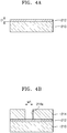
- FIGS. 4A to 4D illustrate a method of forming a 2D material according to example embodiments.
- a transition metal layer 212 is deposited on the substrate 210 to a desired (and/or alternatively predetermined) thickness t1.
- the transition metal layer 212 may be deposited to a particular thickness or more to allow a 2D material (220 in FIG. 4D ) to vertically grow from the substrate 210, as described below. Meanwhile, when the transition metal layer 212 has a thickness less than the particular thickness, a 2D material aligned parallel to the substrate 210 may be formed.
- the transition metal layer 212 may have the thickness t1 of about 3 nm to about 12 nm to form the 2D material 220 that is vertically aligned on the substrate 210.
- example embodiments are not limited thereto.
- a guide pattern layer 214 including a trench 214A is formed in the transition metal layer 212.
- a guide pattern layer 214 covers the transition metal layer 212.
- the guide pattern layer 214 may include a material having no reactivity to the transition metal layer 212, for example, an insulation material.
- a trench 214A that exposes the transition metal layer 212 has a desired (and/or alternatively predetermined) width W1 by patterning the guide pattern layer 214 in a desired (and/or alternatively predetermined) shape.
- the trench 214A formed in the guide pattern layer 214 may guide a plurality of layers forming the 2D material 220 of FIG.
- the width W1 of the trench 214A may be equal to or less than about 10 nm. However, example embodiments are not limited thereto.
- the 2D material 220 that is vertically aligned with the substrate 210 is formed within the trench 214A from the transition metal layer 212 that is exposed through the trench 214A.
- the 2D material 220 may include a plurality of layers that are vertically aligned with respect to the substrate 210 and the layers may be formed with directivity and in parallel to each other.
- the 2D material 220 may denote a semiconductor material having a 2D crystal structure.
- the 2D material 220 may include TMD.
- TMD may include one of metal elements of Mo, W, Nb, V, Ta, Ti, Zr, Hf, Tc, Re, Cu, Ga, In, Sn, Ge, and Pb and one of chalcogen elements of S, Se, and Te.
- the above-described materials are merely non-limiting examples and other materials may be used for TMD.
- the 2D material 220 may be doped with impurities.
- the 2D material 220 may be doped with a p-type dopant or an n-type dopant.
- a p-type dopant and an n-type dopant used for graphene or carbon nanotube (CNT), for example, may be used as the p-type dopant and the n-type dopant.
- the 2D material 220 may be formed by a chemical vapor deposition (CVD) method, in detail, a thermal CVD method.
- CVD chemical vapor deposition
- the thermal CVD method of forming the 2D material 220 that is vertically aligned on the substrate 210 is described below.
- a case of forming a MoS 2 2D material 220 that is vertically aligned on the substrate 210 from a Mo transition metal layer 212 is described as an example.
- a structure illustrated in FIG. 4B and sulfur powder 250 are provided within a tube furnace (not shown).
- the sulfur powder 250 is heated to a desired (and/or alternatively predetermined) temperature, for example, about 600°C to about 1000°C
- the sulfur powder 250 is vaporized and sulfur vapor is moved along a flow of an inert gas, for example, Ar, into the trench 214A.
- an inert gas for example, Ar
- the sulfur stream flowing into the trench 214A generates sulfurization by contacting the Mo transition metal layer 212 and thus, as illustrated in FIG. 4D , the MoS 2 2D material 220 grows within the trench 214A.
- a process temperature of the tube furnace may be about 600°C to about 1000°C.
- the MoS 2 2D material 220 including a plurality of layers vertically aligned with respect to the substrate 210 may be formed in the trench 214A.
- the layers forming the MoS2 2D material 220 may be formed with a desired (and/or alternatively predetermined) directivity and in parallel to each other by the trench 214A formed in the guide pattern layer 214.
- the 2D material 220 vertically aligned in the trench 214A may have a height roughly twice the thickness t1 of the transition metal layer 212, but example embodiments are not limited thereto.
- the transition metal layer 212 and the guide pattern layer 214 around the 2D material 220 may be removed. Accordingly, only the 2D material 220 that is vertically aligned may be left on the substrate 210.
- FIGS. 5A to 5D illustrate a method of forming a 2D material according to example embodiments.
- a guide pattern layer 314 including a trench 314A (e.g., opening) is formed on the substrate 310.
- the guide pattern layer 314 covers the substrate 310.
- the guide pattern layer 314 may include, for example, an insulation material.
- the trench 314A that exposes the substrate 310 has a desired (and/or alternatively predetermined) width W2 by patterning the guide pattern layer 314.
- the trench 314A formed in the guide pattern layer 314 may guide a plurality of layers forming a 2D material 320 of FIG. 5D to be described layer, to be formed with a desired (and/or alternatively predetermined) directivity and in parallel to each other.
- the trench 314A may have the width of about 10 nm or less. However, example embodiments are not limited thereto.
- a transition metal layer 312 is deposited on the substrate 310 that is exposed through the trench 314A.
- the transition metal layer 312 formed in the trench 314A may be deposited to a desired (and/or alternatively predetermined) thickness t2 to grow the 2D material 320 vertically with respect to the substrate 310, as described below.
- the transition metal layer 312 may be deposited to a thickness t2 of about 3 nm to about 12 nm.
- example embodiments are not limited thereto.
- the deposited transition metal layer 312 may be exposed through the trench 314A.
- the 2D material 320 that is vertically aligned with respect to the substrate 310 within the trench 314A is formed from the transition metal layer 312 that is exposed through the trench 314A.
- the 2D material 320 may include a plurality of layers that are vertically aligned with respect to the substrate 310, and the layers may be formed with a desired (and/or alternatively predetermined) directivity and in parallel to each other.
- the 2D material 320 may include TMD.
- TMD may include one of metal elements of Mo, W, Nb, V, Ta, Ti, Zr, Hf, Tc, Re, Cu, Ga, In, Sn, Ge, and Pb and one of chalcogen elements of S, Se, and Te.
- example embodiments are not limited thereto.
- the 2D material 320 may be doped with impurities.
- the 2D material 320 may be formed by a CVD method, in detail, a thermal CVD method.
- a method of forming the 2D material 320 that is vertically aligned on the substrate 310 by the thermal CVD method is described below.
- a case of forming a MoS 2 2D material 320 that is vertically aligned on the substrate 310 from a Mo transition metal layer 312 is described as an example.
- a structure illustrated in FIG. 5B and sulfur powder 350 are provided within a tube furnace (not shown).
- the sulfur powder 350 is heated to a desired (and/or alternatively predetermined) temperature, for example, about 600°C to about 1000°C
- the sulfur powder 350 is vaporized and sulfur vapor is moved along a flow of an inert gas (e.g., Ar) into the trench 314A.
- an inert gas e.g., Ar
- the sulfur stream flowing into the trench 314A generates sulfurization by contacting the Mo transition metal layer 312 and thus, as illustrated in FIG. 5D , the MoS 2 2D material 320 grows within the trench 314A.
- a process temperature of the tube furnace may be about 600°C to about 1000°C.
- the MoS2 2D material 320 growing within the trench 314A may include a plurality of layers vertically aligned with respect to the substrate 310. Also, the layers forming the MoS2 2D material 320 may be formed with a desired (and/or alternatively predetermined) directivity and in parallel to each other by the trench 314A formed in the guide pattern layer 314.
- the 2D material 320 vertically aligned in the trench 314A may have a height roughly twice a thickness of the transition metal layer 312, but example embodiments are not limited thereto.
- the guide pattern layer 314 around the 2D material 320 may be removed. Accordingly, only the 2D material 320 that is vertically aligned may be left on the substrate 310.
- FIGS. 6A to 6C illustrate a method of forming a 2D material according to an example not forming part of the claimed invention.
- a transition metal layer 412 having a desired (and/or alternatively predetermined) width W3 and a desired (and/or alternatively predetermined) thickness t3 is formed on the substrate 410.
- the transition metal layer 412 may be formed as follows. First, the transition metal layer 412 is deposited to cover the substrate 410. The transition metal layer 412 may be deposited to the desired (and/or alternatively predetermined) thickness t3, to grow a 2D material 420 to be described later to be vertically on the substrate 410. For example, the transition metal layer 412 may be deposited to the desired (and/or alternatively predetermined) thickness t3 of about 3 nm to about 12 nm.
- the transition metal layer 412 having a desired (and/or alternatively predetermined) width W3 is formed on the substrate 410 through a patterning process.
- the transition metal layer 412 may have a width W3 of, for example, about 10 nm or less, but example embodiments are not limited thereto.
- the 2D material 420 that is vertically aligned on the substrate 410 is formed from the transition metal layer 412 having the desired (and/or alternatively predetermined) width W3 and the desired (and/or alternatively predetermined) thickness t3 that is formed on the substrate 410.
- the 2D material 420 may include a plurality of layers that are vertically aligned with respect to the substrate 410, and the layers may be formed with a desired (and/or alternatively predetermined) directivity and in parallel to each other
- the 2D material 420 may include TMD.
- TMD may include one of metal elements of Mo, W, Nb, V, Ta, Ti, Zr, Hf, Tc, Re, Cu, Ga, In, Sn, Ge, and Pb and one of chalcogen elements of S, Se, and Te.
- example embodiments are not limited thereto.
- the 2D material 420 may be doped with impurities.
- the 2D material 420 may be formed by a CVD method, in detail, a thermal CVD method.
- a method of forming the 2D material 420 that is vertically aligned on the substrate 410 by the thermal CVD method is described below.
- a case of forming a MoS 2 2D material 420 that is vertically aligned on the substrate 410 from a Mo transition metal layer 412 is described as an example.
- a structure illustrated in FIG. 6A and sulfur powder 450 are provided within a tube furnace (not shown).
- the sulfur powder 450 is heated to a desired (and/or alternatively predetermined) temperature, for example, about 600°C to about 1000°C, the sulfur powder 450 is vaporized and sulfur vapor is moved along a flow of an inert gas, for example, Ar, to contact the Mo transition metal layer 412 generating sulfurization. Accordingly, as illustrated in FIG. 6C , the MoS 2 2D material 420 grows.
- a process temperature of the tube furnace may be about 600°C to about 1000°C.
- the MoS 2 2D material 420 may include a plurality of layers vertically aligned with respect to the substrate 410. Also, since the transition metal layer 412 has the desired (and/or alternatively predetermined) width W3, for example, about 10 nm or less, the layers forming the MoS 2 2D material 420 may be formed with a desired (and/or alternatively predetermined) directivity and in parallel to each other.
- FIGS. 7A to 7C illustrate a method of manufacturing a transistor according to example embodiments.
- a 2D material 520 that is vertically aligned is formed on a substrate 510.
- a silicon substrate, on which an oxide layer is formed, for example, may be used as the substrate 510.
- example embodiments are not limited thereto and a substrate formed of other various materials may be used therefor.
- the 2D material 520 including at least one layer that is vertically aligned with respect to the substrate 510 is provided on an upper surface of the substrate 510. Since the 2D material 520 is described above, a detailed description thereof is omitted.
- a gate insulation layer 525 is deposited on the substrate 510 and the 2D material 520.
- the gate insulation layer 525 may cover an upper surface and side surfaces of the 2D material 520.
- the gate insulation layer 525 may include, for example, a silicon oxide, a silicon nitride, an aluminum oxide, a hafnium oxide, or an insulating polymer. However, this is merely exemplary and the gate insulation layer 525 may include various insulation materials.
- a gate electrode 530 is deposited on the gate insulation layer 525.
- the gate electrode 530 may be provided corresponding to upper surface and side surfaces of the 2D material 520.
- the gate electrode 530 may include a metal material exhibiting superior electrical conductivity, for example, Ag, Au, Pt, or Cu. However, example embodiments are not limited thereto.
- a source electrode and a drain electrode are formed at opposite ends of the 2D material 520.
- the source electrode and the drain electrode may be simultaneously formed with the gate electrode 530.
- FIGS. 8A to 8D illustrate a method of forming a 2D material according to example embodiments.
- a guide pattern layer 614 that exposes a surface of the substrate 610 is formed on the substrate 610.
- the guide pattern layer 614 includes a side surface 614A that is substantially vertical with respect to the surface of the substrate 610.
- a transition metal layer 612 is deposited to cover the substrate 610 and the guide pattern layer 614. In this case, angled deposition may be performed on the side surface 614A of the guide pattern layer 614 to facilitate deposition of the transition metal layer 612.
- the transition metal layer 612 formed on an upper surface of the guide pattern layer 614 and an upper surface of the substrate 610 are removed by etching so that the transition metal layer 612 may remain only on the side surface 614A of the guide pattern layer 614.
- the transition metal layer 612 may be etched by, for example, plasma, but not limited thereto.
- the transition metal layer 612 remaining on the side surface 614A of the guide pattern layer 614 through etching may have a desired (and/or alternatively predetermined) thickness t4.
- the transition metal layer 612 may have the desired (and/or alternatively predetermined) thickness t4 that is less than a specific thickness of the side surface 614A of the guide pattern layer 614.
- the transition metal layer 612 may have the desired (and/or alternatively predetermined) thickness t4 that is less than, for example, about 3 nm. However, example embodiments are not limited thereto. As such, when the transition metal layer 612 has the desired (and/or alternatively predetermined) thickness t4 that is less than a specific thickness, as described below, a 2D material that is aligned in parallel to the side surface 614A of the guide pattern layer 614 may be formed from the transition metal layer 612. Accordingly, a 2D material 620 that is aligned substantially vertically may be formed on the substrate 610.
- the 2D material 620 is grown from the transition metal layer 612 by a CVD method, in detail, a thermal CVD method. Since the transition metal layer 612 has the desired (and/or alternatively predetermined) thickness t4, for example, less than 3 nm, the 2D material 620 formed from the transition metal layer 612 may grow to be substantially parallel to the side surface 614A of the guide pattern layer 614, that is, substantially vertically with respect to the substrate 610.
- the 2D material 620 may include a monolayer or a few layers. As described above, the 2D material 620 may include TMD.
- TMD may include one of metal elements of Mo, W, Nb, V, Ta, Ti, Zr, Hf, Tc, Re, Cu, Ga, In, Sn, Ge, and Pb and one of chalcogen elements of S, Se, and Te.
- the 2D material 620 may be doped with impurities.
- the guide pattern layer 614 remaining around the 2D material 620 may be removed. Accordingly, only the 2D material 620 that is vertically aligned may be left on the substrate 610.
- FIGS. 9A to 9C illustrate a method of forming a 2D material according to an example not forming part of the claimed invention.
- a guide pattern layer 714 that exposes a surface of the substrate 710 is formed on the substrate 710.
- the guide pattern layer 714 includes a side surface 714A that is substantially vertical with respect to the surface of the substrate 710.
- a 2D material 720 is deposited to cover the substrate 710 and the guide pattern layer 714.
- the 2D material 720 may include a monolayer or a few layers.
- the 2D material 720 that is substantially vertically aligned on the substrate 710 may be formed on the side surface 714A of the guide pattern layer 714, through the deposition of the 2D material 720.
- the respective layers forming the 2D material 720 are formed in parallel to the side surface 714A of the guide pattern layer 714.
- the 2D material 720 that is vertically formed with respect to the substrate 710 may have the desired (and/or alternatively predetermined) thickness t5 on the side surface 714A of the guide pattern layer 714.
- the 2D material 720 may include TMD, as described above.
- TMD may include one of metal elements of Mo, W, Nb, V, Ta, Ti, Zr, Hf, Tc, Re, Cu, Ga, In, Sn, Ge, and Pb and one of chalcogen elements of S, Se, and Te.
- the 2D material 720 may be doped with impurities.
- the 2D material 720 remaining on an upper surface of the guide pattern layer 714 and an upper surface of the substrate 710 is removed by etching
- the 2D material 720 that is substantially vertically aligned with respect to the substrate 710 is left on the side surface 714A of the guide pattern layer 714.
- the guide pattern layer 714 remaining around the 2D material 720 may be removed. Accordingly, only the 2D material 720 that is vertically aligned on the substrate 710 may remain on the substrate 710.
- FIGS. 10A to 10D illustrate a method of manufacturing a transistor according to an example not forming part of the claimed invention.
- FIGS. 10A to 10D illustrate a method of manufacturing a transistor from the structure illustrated in FIG. 8C or FIG. 9C .
- a guide pattern layer 814 formed of an insulation material and having a side surface 814A that is substantially vertical with respect to a substrate 810 is formed on the substrate 810.
- a 2D material 820 is formed on the side surface 814A of the guide pattern layer 814.
- the 2D material 820 may include a monolayer or a few layers and the respective layers may be substantially vertically aligned on the substrate 810.
- an insulation material is deposited to cover the 2D material 820 and the substrate 810, thereby forming a dielectric layer 815.
- a gate insulation layer 816 is formed by etching the dielectric layer 815.
- the gate electrode 830 is deposited on the gate insulation layer 816.
- the gate electrode 830 may be formed on an upper surface and side surfaces of the 2D material 820.
- the gate electrode 830 may include, for example, a metal material exhibiting superior electrical conductivity. However, example embodiments are not limited thereto.
- FIG. 11 is a perspective view of a gas sensor 900 according to example embodiments.
- FIG. 12 is a cross-sectional view taken along a line XII-XII' of FIG. 11 .
- the gas sensor 900 may include a substrate 910, a plurality of 2D materials 920 provided on the substrate 910, and first and second electrodes 941 and 942 provided on opposite ends of the 2D materials 920.
- a heater 970 for heating the 2D materials 920 to a desired (and/or alternatively predetermined) temperature may be further provided on the substrate 910.
- the 2D materials 920 are provided on the substrate 910.
- the 2D materials 920 may be arranged spaced apart from each other with a desired (and/or alternatively predetermined) interval.
- FIG. 11 illustrates a case in which the 2D materials 920 are provided on the substrate 910, if necessary, only one 2D material 920 may be provided on the substrate 910.
- the 2D materials 920 each denote a semiconductor material having a 2D crystal structure and may have a monolayer or multilayer structure, as described above. Each layer forming the 2D materials 920 may have a thickness of an atomic level. The layers forming the 2D materials 920 may be connected by the Van Der Waals bond.
- the 2D materials 920 may include TMD.
- TMD may include one of metal elements of Mo, W, Nb, V, Ta, Ti, Zr, Hf, Tc, Re, Cu, Ga, In, Sn, Ge, and Pb and one of chalcogen elements of S, Se, and Te.
- the above-described materials are merely a non-limiting example and other materials may be used for TMD.
- the 2D materials 920 may be doped with a p-type dopant or an n-type dopant to control mobility.
- a p-type dopant and an n-type dopant used for graphene or CNT, for example, may be used as the p-type dopant and the n-type dopant.
- the p-type dopant or the n-type dopant may be doped by an ion implantation method or a chemical doping method.
- the 2D materials 920 may have characteristics of adsorbing various types of gases.
- each layer forming the 2D materials 920 may be substantially vertically aligned with respect to the substrate 910.
- the 2D materials 920 may be arranged with a desired (and/or alternatively predetermined) directivity and in parallel to each other.
- surfaces of the 2D materials 920 may have a high reactivity. Accordingly, since various types of gases are efficiently adsorbed, the gas sensor 900 of a high efficiency may be implemented.
- First and second electrodes 941 and 941 are provided at opposite ends of the 2D materials 920.
- the electrical characteristics of the 2D materials 920 are changed. The change of the electrical characteristics is measured through the first and second electrodes 941 and 942 and thus whether the gases are adsorbed may be identified.
- the heater 970 for heating the 2D materials 920 may be further provided on the substrate 910.
- the heater 970 may clean the 2D materials 920 that adsorbed gases.
- the gases adsorbed by the 2D materials 920 may be removed from the 2D materials.
- the 2D materials 920 from which the gases are removed may be reused.
- FIG. 12 illustrates that the heater 970 is provided on a lower surface of the substrate 910, the present disclose is not limited thereto and the position of the heater 970 may be variously changed. Also, the shape of the heater 970 provided on the substrate 910 may be variously changed.
- the 2D materials 920 are vertically aligned on the substrate 910 and the layers forming the 2D materials 920 are formed with a desired (and/or alternatively predetermined) directivity and in parallel to each other, various types of gases may be detected with a high efficiency.
- the 2D material used as a channel material is vertically aligned with respect to the substrate and the layers forming the 2D material are formed with a desired (and/or alternatively predetermined) directivity and in parallel to each other, a transistor of a fine size with superior performance, for example, a FinFET having a channel width of about 10 nm or less, may be implemented. Also, a gas sensor capable of detecting various types of gases with a high efficiency may be implemented.
- FIG. 13 is a perspective view of a gas sensor according to example embodiments.
- FIG. 14 is a cross-sectional view taken along a line XIV-XIV' of FIG. 13 .
- the gas sensor 1300 illustrated in FIGS. 13-14 may be the same as the gas sensor 900 in FIGS. 9-10 described above, except for the following differences.
- the gas sensor 1300 may include different types of 2D materials 920 between the first and second electrodes 941 and 942.
- the gas sensor 1300 may include at least two different 2D materials between the first and second electrodes 941 and 942.
- the gas sensor 1300 may include the 2D materials 920, 1320, 1323 and 1325 spaced apart from each other between the first and second electrodes 941 and 942.
- the 2D material 920 may have a different composition than the 2D material 1320.
- the 2D material 920 may include one of metal elements of Mo, W, Nb, V, Ta, Ti, Zr, Hf, Tc, Re, Cu, Ga, In, Sn, Ge, and Pb and one of chalcogen elements of S, Se, and Te.
- the 2D material 1320 may include one of metal elements of Mo, W, Nb, V, Ta, Ti, Zr, Hf, Tc, Re, Cu, Ga, In, Sn, Ge, and Pb and one of chalcogen elements of S, Se, and Te.
- the metal element and/or the chalcogen element in the 2D material 1320 may be different than the metal element and/or the chalcogen element in the 2D material 920.
- the 2D materials 1320 and 1325 may have the same composition, but the 2D material 1320 may be doped differently than the 2D material 1323.
- the 2D materials 1320 and 1325 may have the same composition, but the 2D material 1325 may have more layers than the 2D material 1320.
- FIGS. 15A to 15D illustrate part of a method of manufacturing a transistor according to an example not forming part of the claimed invention.
- a transition metal layer 512 may be formed on a substrate 410. Then a preliminary 2D material 1515 may be grown from the transitional metal layer 512. The preliminary 2D material 1515 may cover an entire surface of the substrate 410. Then, as shown in FIGS. 15C and 15D , the preliminary 2D material 1515 may be patterned by etching a portion of the preliminary 2D material 1515 that is exposed by a mask M1 to form the 2D material 520. After FIG. 15D , the 2D material 520 may be processed according to the operations described with reference to FIGS. 7B and 7C .
Landscapes
- Chemical & Material Sciences (AREA)
- Engineering & Computer Science (AREA)
- Materials Engineering (AREA)
- Metallurgy (AREA)
- Crystallography & Structural Chemistry (AREA)
- Organic Chemistry (AREA)
- Chemical Kinetics & Catalysis (AREA)
- Health & Medical Sciences (AREA)
- Life Sciences & Earth Sciences (AREA)
- Physics & Mathematics (AREA)
- Microelectronics & Electronic Packaging (AREA)
- Inorganic Chemistry (AREA)
- General Chemical & Material Sciences (AREA)
- General Physics & Mathematics (AREA)
- General Health & Medical Sciences (AREA)
- Pathology (AREA)
- Immunology (AREA)
- Biochemistry (AREA)
- Analytical Chemistry (AREA)
- Electrochemistry (AREA)
- Molecular Biology (AREA)
- Thin Film Transistor (AREA)
- Condensed Matter Physics & Semiconductors (AREA)
- Manufacturing & Machinery (AREA)
- Computer Hardware Design (AREA)
- Power Engineering (AREA)
- Plasma & Fusion (AREA)
Claims (14)
- Vorrichtung, umfassend: ein Substrat (110, 910);
ein zweidimensionales Material (120, 920) auf dem Substrat, wobei das zweidimensionale Material mindestens eine Schicht beinhaltet, die eine größere Breite als eine Stärke aufweist und die im Wesentlichen vertikal zu dem Substrat ausgerichtet ist, sodass ein Rand der mindestens einen Schicht auf dem Substrat ist und sich die mindestens eine Schicht im Wesentlichen vertikal zu dem Substrat erstreckt, wobei sich die Breite der mindestens einen Schicht im Wesentlichen vertikal zu dem Substrat erstreckt und die mindestens eine Schicht einen Halbleiter beinhaltet, der eine zweidimensionale Kristallstruktur aufweist;
eine erste Elektrode (141, 941) und eine zweite Elektrode (142, 942), die auf dem Substrat voneinander beabstandet und jeweils mit gegenüberliegenden Enden des zweidimensionalen Materials verbunden sind, dadurch gekennzeichnet, dass die mindestens eine Schicht des zweidimensionalen Materials die erste und zweite Elektrode vertikal berührt. - Vorrichtung nach Anspruch 1, wobei die erste und zweite Elektrode eine Source-Elektrode und eine Drain-Elektrode sind; und ferner umfassend:eine Gate-Isolierschicht (125) auf dem zweidimensionalen Material zwischen der Source-Elektrode und der Drain-Elektrode; undeine Gate-Elektrode (130) auf der Gate-Isolierschicht, und vorzugsweise ist die Gate-Elektrode (130) von der ersten Elektrode (141) und der zweiten Elektrode (142) beabstandet.
- Vorrichtung nach Anspruch 2, wobei die Vorrichtung eine Transistorvorrichtung ist und das zweidimensionale Material (120) eine obere Fläche und Seitenflächen beinhaltet, die Gate-Isolierschicht (125) und die Gate-Elektrode (130) auf der oberen Fläche und den Seitenflächen des zweidimensionalen Materials sind.
- Vorrichtung nach Anspruch 1, wobei die Vorrichtung ein Gassensor (900) ist und das zweidimensionale Material (120, 920) in der Lage ist, ein gewünschtes Gas zu adsorbieren, und wobei die Vorrichtung vorzugsweise ferner Folgendes umfasst:
ein Heizelement (970), das das Substrat (100, 910) berührt, wobei das Heizelement konfiguriert ist, um das gewünschte Gas, das auf dem zweidimensionalen Material adsorbiert ist, durch Erwärmen des zweidimensionalen Materials zu entfernen, und ferner vorzugsweise wobei das zweidimensionale Material über dem Heizelement ist. - Vorrichtung nach einem der vorherigen Ansprüche, wobei das zweidimensionale Material (120, 920) eine Vielzahl von Schichten beinhaltet, die im Wesentlichen vertikal zu dem Substrat ausgerichtet sind, und die Vielzahl von Schichten parallel zueinander sind.
- Vorrichtung nach einem der vorherigen Ansprüche, wobei das zweidimensionale Material ein Übergangsmetall-Dichalcogenid beinhaltet.
- Verfahren zum Bilden eines zweidimensionalen Materials, das Verfahren umfassend:Bilden einer Führungsmusterschicht auf einem Substrat;Abscheiden einer Übergangsmetallschicht auf dem Substrat oder der Führungsmusterschicht; Anwachsen des zweidimensionalen Materials auf dem Substrat oder der Führungsmusterschicht von einem freiliegenden Abschnitt der Übergangsmetallschicht,wobei das zweidimensionale Material mindestens eine Schicht beinhaltet, die eine Breite aufweist, die größer ist als eine Stärke, und die im Wesentlichen vertikal auf dem Substrat ausgerichtet ist, sodass ein Rand der mindestens einen Schicht auf dem Substrat ist und sich die Breite der Schicht im Wesentlichen vertikal zu dem Substrat erstreckt, und die mindestens eine Schicht einen Halbleiter beinhaltet, der eine zweidimensionale Kristallstruktur aufweist, gekennzeichnet durch Bilden einer ersten Elektrode und einer zweiten Elektrode an gegenüberliegenden Enden des zweidimensionalen Materials, sodass die mindestens eine Schicht des zweidimensionalen Materials die erste und zweite Elektrode vertikal berührt.
- Verfahren nach Anspruch 7, wobei die Führungsmusterschicht einen Graben beinhaltet, der die Übergangsmetallschicht auf dem Substrat freilegt; und
wobei das zweidimensionale Material auf dem Substrat aus dem Abschnitt der Übergangsmetallschicht angewachsen, der durch den Graben freigelegt ist, wobei das Anwachsen des zweidimensionalen Materials ein Verwenden eines chemischen Dampfabscheidungsverfahrens beinhaltet, und vorzugsweise wobei die Übergangsmetallschicht eine Stärke von 3 nm bis 12 nm aufweist, und ferner vorzugsweise wobei der Graben eine Breite von 10 nm oder weniger aufweist. - Verfahren nach Anspruch 7, wobei die Führungsmusterschicht eine Seitenfläche aufweist, die im Wesentlichen vertikal in Bezug auf eine Oberfläche des Substrats ist, und ein Anwachsen des zweidimensionalen Materials ein Anwachsen des zweidimensionalen Materials auf der Seitenfläche der Führungsmusterschicht umfasst.
- Verfahren nach Anspruch 7 oder 8, wobei das zweidimensionale Material eine Vielzahl von Schichten beinhaltet, die im Wesentlichen vertikal zu dem Substrat ausgerichtet sind, und die Vielzahl von Schichten parallel zueinander sind.
- Verfahren nach Anspruch 8, wobei das Bilden der Führungsmusterschicht Folgendes beinhaltet:
Abscheiden der Übergangsmetallschicht auf dem Substrat; Bilden der Führungsmusterschicht auf der Übergangsmetallschicht; und Bilden des Grabens in der Führungsmusterschicht, wobei der Graben den Abschnitt der Übergangsmetallschicht freilegt. - Verfahren nach Anspruch 8, wobei das Bilden der Führungsmusterschicht Folgendes beinhaltet:Bilden der Führungsmusterschicht auf dem Substrat;Bilden des Grabens in der Führungsmusterschicht, sodass der Graben das Substrat freilegt; undAbscheiden der Übergangsmetallschicht auf einer Oberfläche des Substrats, die durch den Graben freigelegt ist.
- Verfahren nach Anspruch 9, wobei das Formen des zweidimensionalen Materials Folgendes beinhaltet:Abscheiden einer Übergangsmetallschicht zum Bedecken der Führungsmusterschicht und des Substrats;Ätzen der Übergangsmetallschicht, um zu ermöglichen, dass die Übergangsmetallschicht nur auf einer Seitenfläche der Führungsmusterschicht verbleibt; undBilden des zweidimensionalen Materials aus der Übergangsmetallschicht durch ein chemisches Gasphasenabscheidungsverfahren,und vorzugsweise wobei die Übergangsmetallschicht eine Stärke von weniger als 3 nm aufweist.
- Verfahren nach Anspruch 9, wobei das Formen des zweidimensionalen Materials Folgendes beinhaltet:Abscheiden des zweidimensionalen Materials zum Bedecken der Führungsmusterschicht und des Substrats unter Verwendung eines chemischen Gasphasenabscheidungsverfahrens; undÄtzen des zweidimensionalen Materials, um zu ermöglichen, dass das zweidimensionale Material nur auf einer Seitenfläche der Führungsmusterschicht verbleibt.
Applications Claiming Priority (1)
| Application Number | Priority Date | Filing Date | Title |
|---|---|---|---|
| KR1020150095361A KR102455433B1 (ko) | 2015-07-03 | 2015-07-03 | 수직 정렬된 2차원 물질을 포함하는 소자 및 수직 정렬된 2차원 물질의 형성방법 |
Publications (2)
| Publication Number | Publication Date |
|---|---|
| EP3115484A1 EP3115484A1 (de) | 2017-01-11 |
| EP3115484B1 true EP3115484B1 (de) | 2021-07-07 |
Family
ID=55442642
Family Applications (1)
| Application Number | Title | Priority Date | Filing Date |
|---|---|---|---|
| EP16155085.0A Active EP3115484B1 (de) | 2015-07-03 | 2016-02-10 | Vorrichtung mit vertikal ausgerichtetem zweidimensionalem material und verfahren zur herstellung von vertikal ausgerichtetem zweidimensionalem material |
Country Status (4)
| Country | Link |
|---|---|
| US (1) | US9658186B2 (de) |
| EP (1) | EP3115484B1 (de) |
| KR (1) | KR102455433B1 (de) |
| CN (1) | CN106328708B (de) |
Families Citing this family (28)
| Publication number | Priority date | Publication date | Assignee | Title |
|---|---|---|---|---|
| CN107735864B (zh) | 2015-06-08 | 2021-08-31 | 美商新思科技有限公司 | 衬底和具有3d几何图形上的2d材料沟道的晶体管 |
| US10299205B2 (en) | 2015-11-20 | 2019-05-21 | Geotab Inc. | Big telematics data network communication fault identification method |
| WO2017111869A1 (en) | 2015-12-24 | 2017-06-29 | Intel Corporation | Transition metal dichalcogenides (tmdcs) over iii-nitride heteroepitaxial layers |
| US9882000B2 (en) * | 2016-05-24 | 2018-01-30 | Northrop Grumman Systems Corporation | Wrap around gate field effect transistor (WAGFET) |
| WO2019005074A1 (en) * | 2017-06-29 | 2019-01-03 | Intel Corporation | NON-PLANE TRANSITION METAL DICHALCOGENIC DEVICES |
| KR102608959B1 (ko) | 2017-09-04 | 2023-12-01 | 삼성전자주식회사 | 2차원 물질을 포함하는 소자 |
| KR102334380B1 (ko) | 2017-09-04 | 2021-12-02 | 삼성전자 주식회사 | 2차원 물질을 포함하는 소자의 제조 방법 |
| FR3071353B1 (fr) * | 2017-09-15 | 2020-11-13 | Commissariat Energie Atomique | Transistors a effet de champ avec un canal mince atomique |
| WO2019066935A1 (en) | 2017-09-29 | 2019-04-04 | Intel Corporation | REDUCED CONTACT RESISTANCE GROUP III (N-N) NITRIDE DEVICES AND METHODS OF MAKING THE SAME |
| US11233053B2 (en) | 2017-09-29 | 2022-01-25 | Intel Corporation | Group III-nitride (III-N) devices with reduced contact resistance and their methods of fabrication |
| CN109216483A (zh) * | 2017-11-03 | 2019-01-15 | 北京纳米能源与系统研究所 | 单层MoS2同质结、光探测器及其制备方法、电子元件 |
| CN107919388A (zh) * | 2017-11-15 | 2018-04-17 | 苏州大学 | 降低二维材料场效应晶体管接触电阻的方法 |
| US11988628B2 (en) * | 2018-01-04 | 2024-05-21 | Lyten, Inc. | Container including analyte sensing device |
| US11913901B2 (en) * | 2018-01-04 | 2024-02-27 | Lyten, Inc. | Analyte sensing device |
| TWI644800B (zh) * | 2018-01-15 | 2018-12-21 | 國立臺灣師範大學 | 含有二硫化鉬之生物感測晶片以及應用該生物感測晶片之檢測裝置 |
| US10872973B2 (en) * | 2018-06-28 | 2020-12-22 | Taiwan Semiconductor Manufacturing Co., Ltd. | Semiconductor structures with two-dimensional materials |
| CN111912877B (zh) * | 2019-05-09 | 2024-07-09 | 天津大学 | 基于传感器阵列的有机气体检测识别芯片 |
| US11127747B2 (en) * | 2019-08-23 | 2021-09-21 | Micron Technology, Inc. | Transistors including two-dimensional materials |
| KR20210094330A (ko) | 2020-01-21 | 2021-07-29 | 삼성전자주식회사 | 2차원 반도체 물질을 포함하는 반도체 소자 |
| KR102378177B1 (ko) * | 2020-04-06 | 2022-03-25 | 한국과학기술원 | 수직 방향으로 정렬된 나노패턴을 갖는 2차원 재료의 제조방법 |
| US12176388B2 (en) * | 2020-06-26 | 2024-12-24 | Intel Corporation | Transition metal dichalcogenide nanowires and methods of fabrication |
| US11728391B2 (en) * | 2020-08-07 | 2023-08-15 | Taiwan Semiconductor Manufacturing Co., Ltd. | 2d-channel transistor structure with source-drain engineering |
| US12100755B2 (en) | 2021-04-09 | 2024-09-24 | Taiwan Semiconductor Manufacturing Company, Ltd. | Channel structures including doped 2D materials for semiconductor devices |
| US12310073B2 (en) | 2021-07-09 | 2025-05-20 | Taiwan Semiconductor Manufacturing Company, Ltd. | Transistors having two-dimensional semiconductor channels |
| KR102563569B1 (ko) * | 2021-07-12 | 2023-08-04 | 한양대학교 산학협력단 | 컴팩트 드레인 및 이종 물질 구조에 기반하는 트랜지스터 |
| US20230086499A1 (en) * | 2021-09-20 | 2023-03-23 | Intel Corporation | Thin film transistors having fin structures integrated with 2d channel materials |
| FR3144406B1 (fr) * | 2022-12-22 | 2025-11-07 | Commissariat Energie Atomique | Dispositif microelectronique fet comprenant d’importantes surfaces de contact entre le canal de conduction et les regions de source et drain |
| WO2025214674A1 (en) * | 2024-04-10 | 2025-10-16 | Asml Netherlands B.V. | Method of forming a semiconductor channel and associated apparatus |
Citations (1)
| Publication number | Priority date | Publication date | Assignee | Title |
|---|---|---|---|---|
| US20140106523A1 (en) * | 2012-10-12 | 2014-04-17 | Viktor Koldiaev | Vertical Super-Thin Body Semiconductor on Dielectric Wall Devices and Methods of Their Fabrication |
Family Cites Families (22)
| Publication number | Priority date | Publication date | Assignee | Title |
|---|---|---|---|---|
| US7132678B2 (en) | 2003-03-21 | 2006-11-07 | International Business Machines Corporation | Electronic device including a self-assembled monolayer, and a method of fabricating the same |
| US7202494B2 (en) | 2003-06-26 | 2007-04-10 | Rj Mears, Llc | FINFET including a superlattice |
| US7829951B2 (en) | 2008-11-06 | 2010-11-09 | Qualcomm Incorporated | Method of fabricating a fin field effect transistor (FinFET) device |
| JP5544796B2 (ja) * | 2009-09-10 | 2014-07-09 | ソニー株式会社 | 3端子型電子デバイス及び2端子型電子デバイス |
| JP5708493B2 (ja) * | 2009-11-13 | 2015-04-30 | 富士通株式会社 | 半導体装置及びその製造方法 |
| CN101777583B (zh) * | 2010-02-05 | 2011-09-14 | 电子科技大学 | 一种石墨烯场效应晶体管 |
| WO2012148557A1 (en) | 2011-02-28 | 2012-11-01 | Ada Foundation | Method for preparation of well-dispersed, discrete nanoparticles by spray drying techniques |
| KR101878751B1 (ko) * | 2011-06-27 | 2018-07-17 | 삼성전자주식회사 | 그래핀 구조체 및 그 제조방법과, 그래핀 소자 및 그 제조방법 |
| CN102683217B (zh) * | 2012-05-24 | 2016-06-22 | 中国科学院上海微系统与信息技术研究所 | 一种基于石墨烯的双栅mosfet的制备方法 |
| CN103456677A (zh) * | 2012-06-05 | 2013-12-18 | 中芯国际集成电路制造(上海)有限公司 | 半导体器件及其制造方法 |
| CN103632922A (zh) * | 2012-08-20 | 2014-03-12 | 中国科学院微电子研究所 | 一种半导体结构及其制造方法 |
| KR101367989B1 (ko) | 2012-12-11 | 2014-02-28 | 한국과학기술원 | Ultra-Thin FinFET 제조 방법 및 이를 이용하여 제조된 Ultra-Thin FinFET. |
| WO2014100723A1 (en) * | 2012-12-21 | 2014-06-26 | The Regents Of The University Of California | Vertically stacked heterostructures including graphene |
| US20150323482A1 (en) * | 2012-12-28 | 2015-11-12 | The University Of Tokyo | Gas sensor and gas sensor structural body |
| KR102046362B1 (ko) * | 2013-02-15 | 2019-11-19 | 한국전자통신연구원 | 가스 센서 및 그의 제조방법 |
| TW201438247A (zh) | 2013-03-06 | 2014-10-01 | Sk Innovation Co Ltd | 具有一致圖案排列之奈米粒子的單電子電晶體及其製造方法 |
| US9105480B2 (en) * | 2013-03-14 | 2015-08-11 | Wisconsin Alumni Research Foundation | Methods for the fabrication of graphene nanoribbon arrays using block copolymer lithography |
| KR102144999B1 (ko) * | 2013-11-05 | 2020-08-14 | 삼성전자주식회사 | 이차원 물질과 그 형성방법 및 이차원 물질을 포함하는 소자 |
| CN103837583B (zh) * | 2013-11-13 | 2017-03-08 | 电子科技大学 | 一种双向生长型碳纳米管阵列传感器及其制备方法 |
| CN104022158B (zh) * | 2014-05-27 | 2017-01-25 | 南昌大学 | 一种MoS2薄膜晶体管 |
| JP5888685B2 (ja) | 2014-07-01 | 2016-03-22 | 国立大学法人名古屋大学 | カーボンナノウォールを用いた電子デバイス |
| CN107221564A (zh) * | 2017-06-05 | 2017-09-29 | 国家纳米科学中心 | 一种层状二硫化钼场效应晶体管及其制备方法和应用 |
-
2015
- 2015-07-03 KR KR1020150095361A patent/KR102455433B1/ko active Active
- 2015-12-17 US US14/972,873 patent/US9658186B2/en active Active
-
2016
- 2016-02-10 EP EP16155085.0A patent/EP3115484B1/de active Active
- 2016-02-24 CN CN201610102164.4A patent/CN106328708B/zh active Active
Patent Citations (1)
| Publication number | Priority date | Publication date | Assignee | Title |
|---|---|---|---|---|
| US20140106523A1 (en) * | 2012-10-12 | 2014-04-17 | Viktor Koldiaev | Vertical Super-Thin Body Semiconductor on Dielectric Wall Devices and Methods of Their Fabrication |
Also Published As
| Publication number | Publication date |
|---|---|
| US20170003248A1 (en) | 2017-01-05 |
| CN106328708B (zh) | 2021-10-26 |
| EP3115484A1 (de) | 2017-01-11 |
| KR20170004676A (ko) | 2017-01-11 |
| KR102455433B1 (ko) | 2022-10-17 |
| CN106328708A (zh) | 2017-01-11 |
| US9658186B2 (en) | 2017-05-23 |
Similar Documents
| Publication | Publication Date | Title |
|---|---|---|
| EP3115484B1 (de) | Vorrichtung mit vertikal ausgerichtetem zweidimensionalem material und verfahren zur herstellung von vertikal ausgerichtetem zweidimensionalem material | |
| US11532709B2 (en) | Field effect transistor including channel formed of 2D material | |
| Chen et al. | Fermi-level depinning of 2D transition metal dichalcogenide transistors | |
| KR102466678B1 (ko) | 금속-이차원 물질-반도체의 접합을 포함하는 반도체 소자 | |
| KR102608959B1 (ko) | 2차원 물질을 포함하는 소자 | |
| US12062697B2 (en) | Semiconductor device including two-dimensional semiconductor material | |
| US9595580B2 (en) | Two-dimensional (2D) material element with in-plane metal chalcogenide-based heterojunctions and devices including said element | |
| Liu et al. | Large scale pattern graphene electrode for high performance in transparent organic single crystal field-effect transistors | |
| Chai et al. | Low-resistance electrical contact to carbon nanotubes with graphitic interfacial layer | |
| KR102334380B1 (ko) | 2차원 물질을 포함하는 소자의 제조 방법 | |
| TW202016985A (zh) | 形成二維材料層的方法、場效電晶體及其製造方法 | |
| US20170194144A1 (en) | High performance thin films from solution processible two-dimensional nanoplates | |
| JP2016219805A (ja) | 二次元物質を含む半導体素子及びその製造方法 | |
| KR102771621B1 (ko) | 육방정계 질화붕소의 제조 방법 | |
| KR102370695B1 (ko) | 금속-이차원 물질-반도체의 접합을 포함하는 반도체 소자 | |
| Singh et al. | Two-step process using MOCVD and thermal oxidation to obtain pure-phase Cu2O thin films transistors | |
| US20230081646A1 (en) | Multi bridge channel field effect transistor and method of fabricating the same | |
| CN110323277B (zh) | 场效应晶体管及其制备方法 | |
| KR102817259B1 (ko) | 전이금속 칼코젠 화합물 기반 반도체 소자 및 그 제조방법 | |
| Lee et al. | Fabrication and characterization of low temperature polycrystalline silicon thin film transistors by ink-jet printed nickel-mediated lateral crystallization | |
| KR20240136193A (ko) | 2차원 물질을 포함하는 반도체 소자 및 그 제조방법 | |
| US20170032964A1 (en) | Method for Protecting a Surface of a Substrate and Semiconductor Device |
Legal Events
| Date | Code | Title | Description |
|---|---|---|---|
| PUAI | Public reference made under article 153(3) epc to a published international application that has entered the european phase |
Free format text: ORIGINAL CODE: 0009012 |
|
| STAA | Information on the status of an ep patent application or granted ep patent |
Free format text: STATUS: THE APPLICATION HAS BEEN PUBLISHED |
|
| AK | Designated contracting states |
Kind code of ref document: A1 Designated state(s): AL AT BE BG CH CY CZ DE DK EE ES FI FR GB GR HR HU IE IS IT LI LT LU LV MC MK MT NL NO PL PT RO RS SE SI SK SM TR |
|
| AX | Request for extension of the european patent |
Extension state: BA ME |
|
| STAA | Information on the status of an ep patent application or granted ep patent |
Free format text: STATUS: REQUEST FOR EXAMINATION WAS MADE |
|
| 17P | Request for examination filed |
Effective date: 20170523 |
|
| RBV | Designated contracting states (corrected) |
Designated state(s): AL AT BE BG CH CY CZ DE DK EE ES FI FR GB GR HR HU IE IS IT LI LT LU LV MC MK MT NL NO PL PT RO RS SE SI SK SM TR |
|
| REG | Reference to a national code |
Ref country code: DE Ref legal event code: R079 Ref document number: 602016060200 Country of ref document: DE Free format text: PREVIOUS MAIN CLASS: C30B0029640000 Ipc: H01L0021336000 |
|
| RIC1 | Information provided on ipc code assigned before grant |
Ipc: H01L 29/66 20060101ALI20201211BHEP Ipc: H01L 21/336 20060101AFI20201211BHEP Ipc: H01L 29/16 20060101ALI20201211BHEP Ipc: C30B 29/64 20060101ALI20201211BHEP Ipc: H01L 29/778 20060101ALI20201211BHEP Ipc: H01L 29/78 20060101ALI20201211BHEP Ipc: H01L 51/00 20060101ALI20201211BHEP Ipc: C30B 29/60 20060101ALI20201211BHEP Ipc: C30B 29/46 20060101ALI20201211BHEP Ipc: H01L 29/786 20060101ALI20201211BHEP Ipc: H01L 51/05 20060101ALI20201211BHEP Ipc: H01L 29/24 20060101ALI20201211BHEP Ipc: H01L 29/06 20060101ALI20201211BHEP Ipc: H01L 21/02 20060101ALI20201211BHEP Ipc: H01L 29/12 20060101ALI20201211BHEP Ipc: C30B 25/04 20060101ALI20201211BHEP |
|
| GRAP | Despatch of communication of intention to grant a patent |
Free format text: ORIGINAL CODE: EPIDOSNIGR1 |
|
| STAA | Information on the status of an ep patent application or granted ep patent |
Free format text: STATUS: GRANT OF PATENT IS INTENDED |
|
| INTG | Intention to grant announced |
Effective date: 20210122 |
|
| GRAS | Grant fee paid |
Free format text: ORIGINAL CODE: EPIDOSNIGR3 |
|
| GRAA | (expected) grant |
Free format text: ORIGINAL CODE: 0009210 |
|
| STAA | Information on the status of an ep patent application or granted ep patent |
Free format text: STATUS: THE PATENT HAS BEEN GRANTED |
|
| AK | Designated contracting states |
Kind code of ref document: B1 Designated state(s): AL AT BE BG CH CY CZ DE DK EE ES FI FR GB GR HR HU IE IS IT LI LT LU LV MC MK MT NL NO PL PT RO RS SE SI SK SM TR |
|
| REG | Reference to a national code |
Ref country code: GB Ref legal event code: FG4D |
|
| REG | Reference to a national code |
Ref country code: AT Ref legal event code: REF Ref document number: 1409403 Country of ref document: AT Kind code of ref document: T Effective date: 20210715 |
|
| REG | Reference to a national code |
Ref country code: DE Ref legal event code: R096 Ref document number: 602016060200 Country of ref document: DE |
|
| REG | Reference to a national code |
Ref country code: IE Ref legal event code: FG4D |
|
| REG | Reference to a national code |
Ref country code: LT Ref legal event code: MG9D |
|
| REG | Reference to a national code |
Ref country code: NL Ref legal event code: MP Effective date: 20210707 |
|
| REG | Reference to a national code |
Ref country code: AT Ref legal event code: MK05 Ref document number: 1409403 Country of ref document: AT Kind code of ref document: T Effective date: 20210707 |
|
| PG25 | Lapsed in a contracting state [announced via postgrant information from national office to epo] |
Ref country code: PT Free format text: LAPSE BECAUSE OF FAILURE TO SUBMIT A TRANSLATION OF THE DESCRIPTION OR TO PAY THE FEE WITHIN THE PRESCRIBED TIME-LIMIT Effective date: 20211108 Ref country code: NL Free format text: LAPSE BECAUSE OF FAILURE TO SUBMIT A TRANSLATION OF THE DESCRIPTION OR TO PAY THE FEE WITHIN THE PRESCRIBED TIME-LIMIT Effective date: 20210707 Ref country code: NO Free format text: LAPSE BECAUSE OF FAILURE TO SUBMIT A TRANSLATION OF THE DESCRIPTION OR TO PAY THE FEE WITHIN THE PRESCRIBED TIME-LIMIT Effective date: 20211007 Ref country code: ES Free format text: LAPSE BECAUSE OF FAILURE TO SUBMIT A TRANSLATION OF THE DESCRIPTION OR TO PAY THE FEE WITHIN THE PRESCRIBED TIME-LIMIT Effective date: 20210707 Ref country code: FI Free format text: LAPSE BECAUSE OF FAILURE TO SUBMIT A TRANSLATION OF THE DESCRIPTION OR TO PAY THE FEE WITHIN THE PRESCRIBED TIME-LIMIT Effective date: 20210707 Ref country code: LT Free format text: LAPSE BECAUSE OF FAILURE TO SUBMIT A TRANSLATION OF THE DESCRIPTION OR TO PAY THE FEE WITHIN THE PRESCRIBED TIME-LIMIT Effective date: 20210707 Ref country code: BG Free format text: LAPSE BECAUSE OF FAILURE TO SUBMIT A TRANSLATION OF THE DESCRIPTION OR TO PAY THE FEE WITHIN THE PRESCRIBED TIME-LIMIT Effective date: 20211007 Ref country code: AT Free format text: LAPSE BECAUSE OF FAILURE TO SUBMIT A TRANSLATION OF THE DESCRIPTION OR TO PAY THE FEE WITHIN THE PRESCRIBED TIME-LIMIT Effective date: 20210707 Ref country code: RS Free format text: LAPSE BECAUSE OF FAILURE TO SUBMIT A TRANSLATION OF THE DESCRIPTION OR TO PAY THE FEE WITHIN THE PRESCRIBED TIME-LIMIT Effective date: 20210707 Ref country code: SE Free format text: LAPSE BECAUSE OF FAILURE TO SUBMIT A TRANSLATION OF THE DESCRIPTION OR TO PAY THE FEE WITHIN THE PRESCRIBED TIME-LIMIT Effective date: 20210707 Ref country code: HR Free format text: LAPSE BECAUSE OF FAILURE TO SUBMIT A TRANSLATION OF THE DESCRIPTION OR TO PAY THE FEE WITHIN THE PRESCRIBED TIME-LIMIT Effective date: 20210707 |
|
| PG25 | Lapsed in a contracting state [announced via postgrant information from national office to epo] |
Ref country code: PL Free format text: LAPSE BECAUSE OF FAILURE TO SUBMIT A TRANSLATION OF THE DESCRIPTION OR TO PAY THE FEE WITHIN THE PRESCRIBED TIME-LIMIT Effective date: 20210707 Ref country code: LV Free format text: LAPSE BECAUSE OF FAILURE TO SUBMIT A TRANSLATION OF THE DESCRIPTION OR TO PAY THE FEE WITHIN THE PRESCRIBED TIME-LIMIT Effective date: 20210707 Ref country code: GR Free format text: LAPSE BECAUSE OF FAILURE TO SUBMIT A TRANSLATION OF THE DESCRIPTION OR TO PAY THE FEE WITHIN THE PRESCRIBED TIME-LIMIT Effective date: 20211008 |
|
| REG | Reference to a national code |
Ref country code: DE Ref legal event code: R097 Ref document number: 602016060200 Country of ref document: DE |
|
| PG25 | Lapsed in a contracting state [announced via postgrant information from national office to epo] |
Ref country code: DK Free format text: LAPSE BECAUSE OF FAILURE TO SUBMIT A TRANSLATION OF THE DESCRIPTION OR TO PAY THE FEE WITHIN THE PRESCRIBED TIME-LIMIT Effective date: 20210707 |
|
| PLBE | No opposition filed within time limit |
Free format text: ORIGINAL CODE: 0009261 |
|
| STAA | Information on the status of an ep patent application or granted ep patent |
Free format text: STATUS: NO OPPOSITION FILED WITHIN TIME LIMIT |
|
| PG25 | Lapsed in a contracting state [announced via postgrant information from national office to epo] |
Ref country code: SM Free format text: LAPSE BECAUSE OF FAILURE TO SUBMIT A TRANSLATION OF THE DESCRIPTION OR TO PAY THE FEE WITHIN THE PRESCRIBED TIME-LIMIT Effective date: 20210707 Ref country code: SK Free format text: LAPSE BECAUSE OF FAILURE TO SUBMIT A TRANSLATION OF THE DESCRIPTION OR TO PAY THE FEE WITHIN THE PRESCRIBED TIME-LIMIT Effective date: 20210707 Ref country code: RO Free format text: LAPSE BECAUSE OF FAILURE TO SUBMIT A TRANSLATION OF THE DESCRIPTION OR TO PAY THE FEE WITHIN THE PRESCRIBED TIME-LIMIT Effective date: 20210707 Ref country code: EE Free format text: LAPSE BECAUSE OF FAILURE TO SUBMIT A TRANSLATION OF THE DESCRIPTION OR TO PAY THE FEE WITHIN THE PRESCRIBED TIME-LIMIT Effective date: 20210707 Ref country code: CZ Free format text: LAPSE BECAUSE OF FAILURE TO SUBMIT A TRANSLATION OF THE DESCRIPTION OR TO PAY THE FEE WITHIN THE PRESCRIBED TIME-LIMIT Effective date: 20210707 Ref country code: AL Free format text: LAPSE BECAUSE OF FAILURE TO SUBMIT A TRANSLATION OF THE DESCRIPTION OR TO PAY THE FEE WITHIN THE PRESCRIBED TIME-LIMIT Effective date: 20210707 |
|
| 26N | No opposition filed |
Effective date: 20220408 |
|
| PG25 | Lapsed in a contracting state [announced via postgrant information from national office to epo] |
Ref country code: IT Free format text: LAPSE BECAUSE OF FAILURE TO SUBMIT A TRANSLATION OF THE DESCRIPTION OR TO PAY THE FEE WITHIN THE PRESCRIBED TIME-LIMIT Effective date: 20210707 |
|
| PG25 | Lapsed in a contracting state [announced via postgrant information from national office to epo] |
Ref country code: MC Free format text: LAPSE BECAUSE OF FAILURE TO SUBMIT A TRANSLATION OF THE DESCRIPTION OR TO PAY THE FEE WITHIN THE PRESCRIBED TIME-LIMIT Effective date: 20210707 |
|
| REG | Reference to a national code |
Ref country code: CH Ref legal event code: PL |
|
| REG | Reference to a national code |
Ref country code: BE Ref legal event code: MM Effective date: 20220228 |
|
| PG25 | Lapsed in a contracting state [announced via postgrant information from national office to epo] |
Ref country code: LU Free format text: LAPSE BECAUSE OF NON-PAYMENT OF DUE FEES Effective date: 20220210 |
|
| PG25 | Lapsed in a contracting state [announced via postgrant information from national office to epo] |
Ref country code: LI Free format text: LAPSE BECAUSE OF NON-PAYMENT OF DUE FEES Effective date: 20220228 Ref country code: IE Free format text: LAPSE BECAUSE OF NON-PAYMENT OF DUE FEES Effective date: 20220210 Ref country code: CH Free format text: LAPSE BECAUSE OF NON-PAYMENT OF DUE FEES Effective date: 20220228 |
|
| PG25 | Lapsed in a contracting state [announced via postgrant information from national office to epo] |
Ref country code: BE Free format text: LAPSE BECAUSE OF NON-PAYMENT OF DUE FEES Effective date: 20220228 |
|
| P01 | Opt-out of the competence of the unified patent court (upc) registered |
Effective date: 20230530 |
|
| PG25 | Lapsed in a contracting state [announced via postgrant information from national office to epo] |
Ref country code: HU Free format text: LAPSE BECAUSE OF FAILURE TO SUBMIT A TRANSLATION OF THE DESCRIPTION OR TO PAY THE FEE WITHIN THE PRESCRIBED TIME-LIMIT; INVALID AB INITIO Effective date: 20160210 |
|
| PG25 | Lapsed in a contracting state [announced via postgrant information from national office to epo] |
Ref country code: MK Free format text: LAPSE BECAUSE OF FAILURE TO SUBMIT A TRANSLATION OF THE DESCRIPTION OR TO PAY THE FEE WITHIN THE PRESCRIBED TIME-LIMIT Effective date: 20210707 Ref country code: CY Free format text: LAPSE BECAUSE OF FAILURE TO SUBMIT A TRANSLATION OF THE DESCRIPTION OR TO PAY THE FEE WITHIN THE PRESCRIBED TIME-LIMIT Effective date: 20210707 |
|
| PG25 | Lapsed in a contracting state [announced via postgrant information from national office to epo] |
Ref country code: MT Free format text: LAPSE BECAUSE OF FAILURE TO SUBMIT A TRANSLATION OF THE DESCRIPTION OR TO PAY THE FEE WITHIN THE PRESCRIBED TIME-LIMIT Effective date: 20210707 |
|
| REG | Reference to a national code |
Ref country code: DE Ref legal event code: R079 Ref document number: 602016060200 Country of ref document: DE Free format text: PREVIOUS MAIN CLASS: H01L0021336000 Ipc: H10D0030010000 |
|
| PGFP | Annual fee paid to national office [announced via postgrant information from national office to epo] |
Ref country code: DE Payment date: 20250121 Year of fee payment: 10 |
|
| PGFP | Annual fee paid to national office [announced via postgrant information from national office to epo] |
Ref country code: FR Payment date: 20250121 Year of fee payment: 10 |
|
| PGFP | Annual fee paid to national office [announced via postgrant information from national office to epo] |
Ref country code: GB Payment date: 20250116 Year of fee payment: 10 |
|
| PG25 | Lapsed in a contracting state [announced via postgrant information from national office to epo] |
Ref country code: TR Free format text: LAPSE BECAUSE OF FAILURE TO SUBMIT A TRANSLATION OF THE DESCRIPTION OR TO PAY THE FEE WITHIN THE PRESCRIBED TIME-LIMIT Effective date: 20210707 |