EP3092667B1 - Thin led flash for camera - Google Patents
Thin led flash for camera Download PDFInfo
- Publication number
- EP3092667B1 EP3092667B1 EP14833271.1A EP14833271A EP3092667B1 EP 3092667 B1 EP3092667 B1 EP 3092667B1 EP 14833271 A EP14833271 A EP 14833271A EP 3092667 B1 EP3092667 B1 EP 3092667B1
- Authority
- EP
- European Patent Office
- Prior art keywords
- led die
- reflector
- led
- lens
- light
- Prior art date
- Legal status (The legal status is an assumption and is not a legal conclusion. Google has not performed a legal analysis and makes no representation as to the accuracy of the status listed.)
- Active
Links
Images


Classifications
-
- H—ELECTRICITY
- H10—SEMICONDUCTOR DEVICES; ELECTRIC SOLID-STATE DEVICES NOT OTHERWISE PROVIDED FOR
- H10H—INORGANIC LIGHT-EMITTING SEMICONDUCTOR DEVICES HAVING POTENTIAL BARRIERS
- H10H20/00—Individual inorganic light-emitting semiconductor devices having potential barriers, e.g. light-emitting diodes [LED]
- H10H20/80—Constructional details
- H10H20/85—Packages
- H10H20/855—Optical field-shaping means, e.g. lenses
- H10H20/856—Reflecting means
-
- G—PHYSICS
- G03—PHOTOGRAPHY; CINEMATOGRAPHY; ANALOGOUS TECHNIQUES USING WAVES OTHER THAN OPTICAL WAVES; ELECTROGRAPHY; HOLOGRAPHY
- G03B—APPARATUS OR ARRANGEMENTS FOR TAKING PHOTOGRAPHS OR FOR PROJECTING OR VIEWING THEM; APPARATUS OR ARRANGEMENTS EMPLOYING ANALOGOUS TECHNIQUES USING WAVES OTHER THAN OPTICAL WAVES; ACCESSORIES THEREFOR
- G03B15/00—Special procedures for taking photographs; Apparatus therefor
- G03B15/02—Illuminating scene
- G03B15/03—Combinations of cameras with lighting apparatus; Flash units
- G03B15/05—Combinations of cameras with electronic flash apparatus; Electronic flash units
-
- G—PHYSICS
- G02—OPTICS
- G02B—OPTICAL ELEMENTS, SYSTEMS OR APPARATUS
- G02B7/00—Mountings, adjusting means, or light-tight connections, for optical elements
- G02B7/02—Mountings, adjusting means, or light-tight connections, for optical elements for lenses
- G02B7/04—Mountings, adjusting means, or light-tight connections, for optical elements for lenses with mechanism for focusing or varying magnification
- G02B7/10—Mountings, adjusting means, or light-tight connections, for optical elements for lenses with mechanism for focusing or varying magnification by relative axial movement of several lenses, e.g. of varifocal objective lens
- G02B7/105—Mountings, adjusting means, or light-tight connections, for optical elements for lenses with mechanism for focusing or varying magnification by relative axial movement of several lenses, e.g. of varifocal objective lens with movable lens means specially adapted for focusing at close distances
-
- H—ELECTRICITY
- H10—SEMICONDUCTOR DEVICES; ELECTRIC SOLID-STATE DEVICES NOT OTHERWISE PROVIDED FOR
- H10H—INORGANIC LIGHT-EMITTING SEMICONDUCTOR DEVICES HAVING POTENTIAL BARRIERS
- H10H20/00—Individual inorganic light-emitting semiconductor devices having potential barriers, e.g. light-emitting diodes [LED]
- H10H20/80—Constructional details
- H10H20/85—Packages
- H10H20/8506—Containers
-
- H—ELECTRICITY
- H10—SEMICONDUCTOR DEVICES; ELECTRIC SOLID-STATE DEVICES NOT OTHERWISE PROVIDED FOR
- H10H—INORGANIC LIGHT-EMITTING SEMICONDUCTOR DEVICES HAVING POTENTIAL BARRIERS
- H10H20/00—Individual inorganic light-emitting semiconductor devices having potential barriers, e.g. light-emitting diodes [LED]
- H10H20/80—Constructional details
- H10H20/85—Packages
- H10H20/851—Wavelength conversion means
- H10H20/8511—Wavelength conversion means characterised by their material, e.g. binder
- H10H20/8512—Wavelength conversion materials
-
- H—ELECTRICITY
- H10—SEMICONDUCTOR DEVICES; ELECTRIC SOLID-STATE DEVICES NOT OTHERWISE PROVIDED FOR
- H10H—INORGANIC LIGHT-EMITTING SEMICONDUCTOR DEVICES HAVING POTENTIAL BARRIERS
- H10H20/00—Individual inorganic light-emitting semiconductor devices having potential barriers, e.g. light-emitting diodes [LED]
- H10H20/80—Constructional details
- H10H20/85—Packages
- H10H20/851—Wavelength conversion means
- H10H20/8514—Wavelength conversion means characterised by their shape, e.g. plate or foil
-
- H—ELECTRICITY
- H10—SEMICONDUCTOR DEVICES; ELECTRIC SOLID-STATE DEVICES NOT OTHERWISE PROVIDED FOR
- H10H—INORGANIC LIGHT-EMITTING SEMICONDUCTOR DEVICES HAVING POTENTIAL BARRIERS
- H10H20/00—Individual inorganic light-emitting semiconductor devices having potential barriers, e.g. light-emitting diodes [LED]
- H10H20/80—Constructional details
- H10H20/85—Packages
- H10H20/851—Wavelength conversion means
- H10H20/8515—Wavelength conversion means not being in contact with the bodies
-
- H—ELECTRICITY
- H10—SEMICONDUCTOR DEVICES; ELECTRIC SOLID-STATE DEVICES NOT OTHERWISE PROVIDED FOR
- H10H—INORGANIC LIGHT-EMITTING SEMICONDUCTOR DEVICES HAVING POTENTIAL BARRIERS
- H10H20/00—Individual inorganic light-emitting semiconductor devices having potential barriers, e.g. light-emitting diodes [LED]
- H10H20/80—Constructional details
- H10H20/85—Packages
- H10H20/855—Optical field-shaping means, e.g. lenses
-
- G—PHYSICS
- G03—PHOTOGRAPHY; CINEMATOGRAPHY; ANALOGOUS TECHNIQUES USING WAVES OTHER THAN OPTICAL WAVES; ELECTROGRAPHY; HOLOGRAPHY
- G03B—APPARATUS OR ARRANGEMENTS FOR TAKING PHOTOGRAPHS OR FOR PROJECTING OR VIEWING THEM; APPARATUS OR ARRANGEMENTS EMPLOYING ANALOGOUS TECHNIQUES USING WAVES OTHER THAN OPTICAL WAVES; ACCESSORIES THEREFOR
- G03B2215/00—Special procedures for taking photographs; Apparatus therefor
- G03B2215/05—Combinations of cameras with electronic flash units
- G03B2215/0564—Combinations of cameras with electronic flash units characterised by the type of light source
- G03B2215/0567—Solid-state light source, e.g. LED, laser
-
- H—ELECTRICITY
- H10—SEMICONDUCTOR DEVICES; ELECTRIC SOLID-STATE DEVICES NOT OTHERWISE PROVIDED FOR
- H10H—INORGANIC LIGHT-EMITTING SEMICONDUCTOR DEVICES HAVING POTENTIAL BARRIERS
- H10H20/00—Individual inorganic light-emitting semiconductor devices having potential barriers, e.g. light-emitting diodes [LED]
- H10H20/80—Constructional details
- H10H20/85—Packages
- H10H20/851—Wavelength conversion means
- H10H20/8511—Wavelength conversion means characterised by their material, e.g. binder
Definitions
- This invention relates to packaged phosphor-converted light emitting diodes (pcLEDs) and, in particular, to a packaged pcLED that is useful as a flash for a camera.
- pcLEDs packaged phosphor-converted light emitting diodes
- a common flash is a GaN-based blue LED die mounted in a round reflective cup on a rigid printed circuit board.
- a layer of YAG phosphor (emits yellow-green) fills the cup. Since the LED die is very thin, almost all light is emitted from the top surface of the die.
- a circular Fresnel lens is then positioned over the cup to create a generally conical light emission pattern (having a circular cross-section) to illuminate a subject for the photograph.
- the phosphor is not uniform over the LED die, resulting in color non-uniformity vs. angle.
- the thinness of the flash module is limited.
- the lens must be spaced away from the top surface of the LED die by a certain minimum distance (e.g., the focal length) in order to properly redirect the light. This minimum distance significantly adds to the thickness of the flash module.
- the bottom inner edge of the reflector cup facing the sides of the LED die has a thickness that is typically greater than the height of the LED semiconductor layers, so the inner edge of the cup blocks the side light or reflects it back into the LED die.
- the reflective cup since almost all light is emitted from the top surface of the LED die, the reflective cup has limited usefulness in shaping the beam, and the resulting beam is not very uniform across the field of view of the camera.
- the reflector cup has to have relative high walls to redirect and collimate the "angled" light emitted from the LED die. Any light rays that are not reflected (collimated) spread out at wide angles.
- the high walls of the reflector limit the minimum thickness of the flash module.
- a blue flip-chip LED die has a relatively thick transparent substrate on its top surface. This causes a significant portion of the light emission to be from the sides of the LED die, such as 50% of the total light emission.
- a conformal coating of phosphor is deposited over the top and side surfaces of the LED die to create a uniform white light.
- the pcLED is mounted on a supporting substrate having a metal pattern for connection to the bottom anode and cathode electrodes of the LED die.
- the substrate has bottom metal pads for bonding to a camera's printed circuit board.
- the substrate can be a very thin flex circuit or a rigid substrate such as ceramic.
- a rectangular reflector with rounded corners, is then mounted on the substrate surrounding the rectangular LED die.
- the rectangular reflector has curved walls for redirecting the side LED light into a generally pyramidal beam, having a rectangular cross-section, where the cross-section aspect ratio is similar to the standard aspect ratio of a camera's field of view.
- the reflector is stamped aluminum, where the opening for the LED die has knife edges facing the sides of the LED die so virtually all side light is reflected upward rather than being blocked by the inner edges of the opening. Such a knife edge could not be achieved by a molded reflector cup.
- a thin lens is affixed over the top of the reflector, where the lens has a convex side that faces toward the LED die, so the convex portion does not add thickness to the module.
- the lens not only protects the LED die but increases light extraction due to the convex portion receiving most of the light from the LED die and reflective walls at a substantially normal angle.
- Fresnel lens having a flat surface facing the LED die, there is much less back-reflection.
- the effective optical distance between the lens and the LED die is the sum of the horizontal distance between a side of the LED die and a curved wall of the reflector plus the vertical distance between the curved wall and the lens. Therefore, the lens can be spaced a focal length from the LED die's sides while being much closer to the top surface of the LED die. This allows the flash module to be even thinner.
- the reflector walls can be more widely spaced from the LED die to further reduce the thinness of the module.
- the reflector walls can be made relatively shallow, further reducing the thinness of the module.
- the convex shape of the lens toward the LED die and the closeness of the lens to the LED top surface cause the lens to intercept a wide angle of the Lambertian light emitted from the top surface of the LED die and slightly redirect it toward the center of the beam, if necessary, to further improve the uniformity of the beam.
- the convex shape is designed to optimize the uniformity of light across a desired portion of the generally rectangular beam.
- the lens is not used to significantly shape the beam (but primarily improves uniformity), since the shape of the beam is primarily controlled by the shape of the reflector, in contrast to the prior art.
- the flash module can be made very thin.
- FIG. 1 is an exploded view of a flash module 10 in accordance with one embodiment of the invention.
- a support substrate 12 may be a rigid substrate or a very thin flexible circuit. Using a flexible circuit as the support substrate 12 allows the module 10 to be thinner.
- a metal trace 14 pattern is formed on the substrate 12 to define metal pads 15 and 17 for the bottom anode and cathode electrodes of the flip chip LED die 16 and to define metal pads 19 and 21 for the electrodes of an optional transient voltage suppressor (TVS) chip 18.
- TVS transient voltage suppressor
- the bare LED die 16 such as a GaN-based blue LED die, is then electrically and thermally connected to the substrate 12.
- the TVS chip 18 may also be electrically connected to the substrate 12.
- the LED die 16 is a flip chip die, while according to embodiments not forming part of the claimed invention, other die types, including those with bonding wires, may be used.
- the LED die's bottom electrodes are directly bonded to the metal pads 15 and 17 of the metal trace 14.
- the bare LED die 16 may be first mounted on a submount with more robust bottom metal pads to simplify handling and enable the LED die 16 to be conformally coated with a phosphor layer 20 after bonding to the submount.
- Fig. 1 shows an alternative embodiment not according to the claimed invention where the phosphor layer 20 covers only the top surface of the LED die 16 .
- the phosphor layer 20 may be deposited over the entire substrate 12 and LED die 16 to coat the top and side surfaces of the LED die 16.
- the phosphor layer 20 may be phosphor particles, such as YAG phosphor particles or red and green phosphor particles, infused in a silicone binder.
- the phosphor layer 20 may also serve as an adhesive layer for affixing a reflector 22 to the surface of the substrate 12. In the alternative, a separate adhesive may be used to affix the reflector 22.
- FIG. 1 Various details of the components in Fig. 1 are described with respect to Figs. 2-8 .
- Fig. 2 is a cross-sectional compressed view of the LED die 16 with the conformal phosphor layer 20 in accordance with the claimed invention.
- a flip-chip die is shown in the examples, which is in accordance with the present invention, however, any other type of LED die, including vertical LED dies, lateral LED dies, etc may be used in embodiments not according to the invention.
- the LED die 16 includes a bottom anode electrode 23 bonded to the metal pad 15 (defined as a portion of the metal trace 14 of Fig. 1 ) and includes a bottom cathode electrode 25 bonded to the metal pad 17.
- the pads 15 and 17 are electrically connected by vias 30 and 31 to associated bottom pads 32 and 34, which may be used to solder the flash module 10 to a camera's printed circuit board.
- a thermal pad 36 is formed on the bottom surface of the substrate 12, which may be soldered to a heat sink in the printed circuit board.
- the LED die 16 semiconductor layers are grown on a relatively thick sapphire substrate 40, which may be as thick as 1 mm. This is thicker than a typical growth substrate, since a manufacturer typically uses the thinnest growth substrate practical for reducing costs and maximizing the top emission. Frequently, in the prior art, the growth substrate is completely removed.
- the sapphire substrate 40 is much thicker than required for mechanically supporting the LED semiconductor layers. Other material for a growth substrate may instead be used.
- the top surface and growth surface of the growth substrate 40 may be roughened for increasing light extraction.
- a typical width of the LED die 16 is on the order of 1 mm.
- N-type layers 42 are epitaxially grown over the sapphire substrate 40, followed by an active layer 44, and p-type layers 46. A portions of the active layer 44 and p-type layers 46 are etched away to gain electrical contact to the n-type layers 42 by means of a via 48 leading to the cathode electrode.
- the active layer 44 generates light having a peak wavelength.
- the peak wavelength is a blue wavelength
- the layers 42, 44, and 46 are GaN-based.
- the growth substrate 40 may be removed and replaced by a transparent support substrate, such as glass, affixed to the semiconductor layers by an adhesive (e.g., silicone) or by other techniques.
- a transparent support substrate such as glass
- an adhesive e.g., silicone
- the light exiting the sides of the LED die 16 is made to be preferably about 50% of the total light emission, with 50% of the total light being emitted from the top surface of the LED die 16.
- the percentage of side light is based on the thickness of the substrate 40. The more side light, the more the reflected light from the reflector 22 is adding to the overall beam and the thinner the flash module can be.
- the thickness of the LED semiconductor layers is less than 100 microns (0.1 mm), and typically less than 20 microns, and the substrate 40 thickness is greater than 0.2 mm and up to 1 mm.
- the reflector 22 ( Fig. 1 ) is preferable formed by stamping an aluminum sheet.
- the stamp forms a rectangular opening 52 in the sheet and compresses the surrounding aluminum to form curved sidewalls 54.
- the term "rectangular,” as used herein, includes a square, and includes rectangles with rounded corners.
- the edges of the opening 52 are knife edges (less than 50 microns thick) to limit any back reflection of the light emitted from the sides of the LED die 16/phosphor.
- the opening 52 and curved sidewalls 54 have the same aspect ratio as the camera's field of view, such as 4:3, so the resulting beam will resemble the 4:3 aspect ratio.
- the reflector 22 is then coated with a silver layer for high reflectivity, such as by plating, evaporation, sputtering, etc.
- the footprint of the reflector 22 may be approximately that of the substrate 12 to minimize the size of the flash module 10.
- the reflector 22 is then affixed to the substrate 12 using the phosphor layer 20 (containing silicone) as an adhesive.
- the reflector 22 adds rigidity to the module 10.
- the phosphor layer 20 is then cured.
- a preformed polycarbonate lens 56 is then affixed to the top surface of the reflector 22, such as by silicone.
- the silicone is then cured to complete the flash module 10.
- the lens 56 is rectangular with rounded edges to receive the generally rectangular emission from the reflector 22 and LED die 16.
- the lens 56 has a flat top surface and a bottom surface. A portion of the bottom surface is a convex surface 58 that faces the LED die 16. Thus, the convex surface does not add to the thickness of the module 10.
- the convex surface 58 is rectangular or rectangular with rounded corners, as shown in Fig. 1 .
- the lens had to be spaced relatively far from the top surface of the LED die to properly redirect the light.
- the effective optical distance from the LED die 16 to the lens 56 is the sum of the generally horizontal distance from an LED die side to a reflector wall 54 plus the generally vertical distance from the reflector wall 54 to the lens 58. Accordingly, to make the module 10 even thinner, the reflector walls 54 can be further spaced from the LED die 16 while retaining the same effective optical distance between the sides and the lens 58.
- the lens 56 is designed to improve the uniformity of light across a central portion of the rectangular beam.
- the effective optical distance between the sides of the LED die 16 and the lens 58 is approximately the focal length of the lens 58.
- Dry air (or other gas) fills the gap between the lens 56 and the LED die 16 to obtain a large difference in the indices of refraction at the interface of the lens 56 and the gap to achieve the desired refraction by the lens 56.
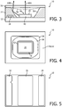
- Fig. 3 shows two sample light rays 60A and 60B.
- Rays, such as 60A from the top center surface of the LED die 16 are not substantially redirected by the lens 56.
- Reflected rays, such as ray 60B, that impinge the convex surface 58 at an angle are slightly redirected toward the center axis to improve the uniformity of the beam across at least a central portion of the 4:3 aspect ratio.
- the shape of the beam is primarily defined by the shape of the reflector 22, since the reflector 22 reflects virtually all side light and some angled light from the top surface of the LED die 16.
- Fig. 3 also shows that the aluminum sheet for forming the reflector 22 is stamped to have a bottom cavity for the TVS chip 18.
- the bottom of the metal reflector 22 does not short out the metal traces 14, and there is no separate step for depositing an adhesive.
- the reflector 22 is formed to have a thin dielectric layer on its bottom surface before being mounted on the substrate 12.
- Fig. 4 is a top down view of the module 10 of Fig. 3 .
- Fig. 5 is a bottom view of the module 10 showing the cathode and anode bottom pads 32 and 34, and the thermal pad 36, also shown in Fig. 2 .
- Fig. 6 is a perspective bisected view of the flash module 10.
- the phosphor layer 20 over the sides of the LED die 16 is not shown.
- Fig. 7 is a perspective view of the flash module 10 of Fig. 1 .
- Fig. 8 is a cross-sectional view of an embodiment of the flash module 10 using a flex substrate 12 and identifying various dimensions in millimeters.
- the LED die 16 is about 1.0 mm in width, the height of the lens 56 above the top surface of the LED die 16 is only about 0.3 mm, since the optimal separation is based on the travel path of the side light to the lens 56 when being reflected off the reflector 22.
- the flex substrate 12 only adds 0.05 mm to the thickness of the module 10.
- the phosphor layer 20 is shown as being 0.05 mm thick.
- the reflector 22 is shown as being 0.750 mm thick, and the lens 56 is shown as adding only 0.1 mm to the module 10.
- the growth substrate 40 ( Fig. 2 ) may be about 0.25-0.5 mm thick.
- the total height of the flash module 10 of Fig. 8 is less than 1 mm. It is envisioned that all practical flash modules of the invention, using a flex circuit, can be formed to have thicknesses less than 2 mm.
- the top surface area of the LED die 16 is about 1 mm 2 and the combined area of the four sides of the LED die, using a 0.5 mm thick substrate 40, is about 2mm 2 .
- the side area equals the top surface area. So there is substantial side emission.
- Fig. 9 is a back view of a smartphone 66, illustrating the rectangular flash module 10 and camera lens 68.
- the present invention reduces the thickness of a flash module, improves the color uniformity across the beam, and increases the efficiency of the flash by creating a generally rectangular beam with a substantially uniform intensity across the relevant portion of the beam and by incurring less reflection of the LED light back toward the LED die.
- the present invention may be used for other applications besides camera flashes, such as a flashlight module.
Landscapes
- Physics & Mathematics (AREA)
- General Physics & Mathematics (AREA)
- Optics & Photonics (AREA)
- Led Device Packages (AREA)
- Stroboscope Apparatuses (AREA)
- Optical Filters (AREA)
Applications Claiming Priority (2)
| Application Number | Priority Date | Filing Date | Title |
|---|---|---|---|
| US201461923925P | 2014-01-06 | 2014-01-06 | |
| PCT/IB2014/067204 WO2015101899A1 (en) | 2014-01-06 | 2014-12-22 | Thin led flash for camera |
Publications (2)
| Publication Number | Publication Date |
|---|---|
| EP3092667A1 EP3092667A1 (en) | 2016-11-16 |
| EP3092667B1 true EP3092667B1 (en) | 2019-04-24 |
Family
ID=52434902
Family Applications (1)
| Application Number | Title | Priority Date | Filing Date |
|---|---|---|---|
| EP14833271.1A Active EP3092667B1 (en) | 2014-01-06 | 2014-12-22 | Thin led flash for camera |
Country Status (6)
Cited By (1)
| Publication number | Priority date | Publication date | Assignee | Title |
|---|---|---|---|---|
| EP3782207B1 (en) * | 2018-04-19 | 2023-06-07 | CreeLED, Inc. | Light-emitting diode package with light-altering material |
Families Citing this family (28)
| Publication number | Priority date | Publication date | Assignee | Title |
|---|---|---|---|---|
| CN105393374B (zh) * | 2013-07-19 | 2019-05-28 | 亮锐控股有限公司 | 具有光学元件并且没有衬底载体的pc led |
| WO2015101899A1 (en) | 2014-01-06 | 2015-07-09 | Koninklijke Philips N.V. | Thin led flash for camera |
| CN103872203A (zh) * | 2014-04-08 | 2014-06-18 | 三安光电股份有限公司 | 具有表面微结构的高亮度发光二极管及其制备和筛选方法 |
| DE102015108499A1 (de) * | 2015-05-29 | 2016-12-01 | Osram Opto Semiconductors Gmbh | Optoelektronisches Bauelement mit einer Strahlungsquelle |
| KR101778848B1 (ko) * | 2015-08-21 | 2017-09-14 | 엘지전자 주식회사 | 발광소자 패키지 어셈블리 및 이의 제조 방법 |
| CN111211206A (zh) * | 2015-09-18 | 2020-05-29 | 新世纪光电股份有限公司 | 发光装置及其制造方法 |
| US9816687B2 (en) * | 2015-09-24 | 2017-11-14 | Intel Corporation | MEMS LED zoom |
| US9746689B2 (en) | 2015-09-24 | 2017-08-29 | Intel Corporation | Magnetic fluid optical image stabilization |
| WO2017095712A1 (en) * | 2015-12-02 | 2017-06-08 | Koninklijke Philips N.V. | Led metal pad configuration for optimized thermal resistance, solder reliability, and smt processing yields |
| US11373990B2 (en) * | 2016-02-29 | 2022-06-28 | Semtech Corporation | Semiconductor device and method of stacking semiconductor die for system-level ESD protection |
| JP2017157684A (ja) * | 2016-03-02 | 2017-09-07 | ローム株式会社 | 発光装置およびその製造方法 |
| DE102016109054A1 (de) * | 2016-05-17 | 2017-11-23 | Osram Opto Semiconductors Gmbh | Verfahren zum Herstellen einer optoelektronischen Leuchtvorrichtung und optoelektronische Leuchtvorrichtung |
| DE102016117523A1 (de) * | 2016-09-16 | 2018-03-22 | Osram Opto Semiconductors Gmbh | Optoelektronisches Bauelement und Verfahren zum Betreiben eines optoelektronischen Bauelements |
| JP6955135B2 (ja) * | 2016-10-19 | 2021-10-27 | 日亜化学工業株式会社 | 発光装置およびその製造方法 |
| US10741644B2 (en) * | 2016-11-22 | 2020-08-11 | Delta Electronics, Inc. | Semiconductor devices with via structure and package structures comprising the same |
| DE102016122770B4 (de) | 2016-11-25 | 2022-01-05 | OSRAM Opto Semiconductors Gesellschaft mit beschränkter Haftung | Bauteil mit einem optoelektronischen Bauelement |
| CN106784258B (zh) * | 2017-03-15 | 2018-11-09 | 厦门大学 | 晶圆级封装led |
| US10950762B2 (en) * | 2017-04-13 | 2021-03-16 | Lightizer Co., Ltd | Round chip scale package and manufacturing method therefor |
| WO2019054934A1 (en) * | 2017-09-18 | 2019-03-21 | Profoto Aktiebolag | FLASH HOUSING AND METHOD OF TRANSMITTING A BEAM LOBE WITH A SUBSTANTIALLY CIRCULAR CROSS SECTION |
| KR102103514B1 (ko) * | 2017-09-27 | 2020-05-29 | 주식회사 시티컴 | 엘이디 광 중화캡 및 그 제조방법 |
| KR102624113B1 (ko) * | 2018-06-08 | 2024-01-12 | 서울바이오시스 주식회사 | 발광 소자 패키지 및 이의 제조 방법 |
| KR102721974B1 (ko) | 2019-08-07 | 2024-10-28 | 삼성전자주식회사 | 광 센서 일체형 플래시 led 패키지 |
| US11435044B2 (en) * | 2019-09-09 | 2022-09-06 | Apple Inc. | Integrated strobe module |
| US11552229B2 (en) | 2020-09-14 | 2023-01-10 | Creeled, Inc. | Spacer layer arrangements for light-emitting diodes |
| KR20220055916A (ko) * | 2020-10-27 | 2022-05-04 | 엘지이노텍 주식회사 | 거리 측정 카메라 장치 |
| EP4250002A4 (en) | 2021-01-07 | 2024-04-24 | Samsung Electronics Co., Ltd. | ELECTRONIC DEVICE FLASH LENS |
| TWI769064B (zh) * | 2021-08-24 | 2022-06-21 | 隆達電子股份有限公司 | 發光裝置 |
| CN115201990A (zh) * | 2022-09-08 | 2022-10-18 | 成都中科卓尔智能科技集团有限公司 | 一种半导体光学材料内部缺陷检测片光源镜头 |
Family Cites Families (45)
| Publication number | Priority date | Publication date | Assignee | Title |
|---|---|---|---|---|
| US4922280A (en) * | 1987-08-26 | 1990-05-01 | Asahi Kogaku Kogyo Kabushiki Kaisha | Infrared filter cover plate for autofocus camera |
| US5303084A (en) * | 1991-08-27 | 1994-04-12 | Kaman Aerospace Corporation | Laser light beam homogenizer and imaging lidar system incorporating same |
| JPH1138897A (ja) * | 1997-07-14 | 1999-02-12 | Beam Denshi Kogyo Kk | 導光板リフレクターおよび導光板リフレクターの貼付方法 |
| US6381415B1 (en) * | 1999-07-21 | 2002-04-30 | Olympus Optical Co., Ltd. | Flash apparatus and camera using the same |
| JP2002299698A (ja) * | 2001-03-30 | 2002-10-11 | Sumitomo Electric Ind Ltd | 発光装置 |
| JP4504662B2 (ja) * | 2003-04-09 | 2010-07-14 | シチズン電子株式会社 | Ledランプ |
| US7157744B2 (en) * | 2003-10-29 | 2007-01-02 | M/A-Com, Inc. | Surface mount package for a high power light emitting diode |
| US20050247944A1 (en) * | 2004-05-05 | 2005-11-10 | Haque Ashim S | Semiconductor light emitting device with flexible substrate |
| DE102005042778A1 (de) * | 2004-09-09 | 2006-04-13 | Toyoda Gosei Co., Ltd., Nishikasugai | Optische Festkörpervorrichtung |
| US8231251B2 (en) * | 2005-10-28 | 2012-07-31 | Philips Lumileds Lighting Company Llc | Multiple piece reflective angle transformer |
| US7600894B1 (en) * | 2005-12-07 | 2009-10-13 | Simon Jerome H | Luminaires and optics for control and distribution of multiple quasi point source light sources such as LEDs |
| JP2007173322A (ja) * | 2005-12-19 | 2007-07-05 | Enplas Corp | 発光装置 |
| US7626210B2 (en) * | 2006-06-09 | 2009-12-01 | Philips Lumileds Lighting Company, Llc | Low profile side emitting LED |
| CN101135833A (zh) * | 2006-08-30 | 2008-03-05 | 台达电子工业股份有限公司 | 用于投影装置的照明系统及包含该照明系统的投影装置 |
| JP4984824B2 (ja) * | 2006-10-26 | 2012-07-25 | 豊田合成株式会社 | 発光装置 |
| CN101617406B (zh) * | 2007-01-17 | 2011-04-20 | 伊利诺伊大学评议会 | 通过基于印刷的组装制造的光学系统 |
| US20080186737A1 (en) * | 2007-02-03 | 2008-08-07 | Awai George K | Edge-illuminated panels with shaped-edge diffuser |
| JP5060172B2 (ja) * | 2007-05-29 | 2012-10-31 | 岩谷産業株式会社 | 半導体発光装置 |
| JP5158472B2 (ja) | 2007-05-24 | 2013-03-06 | スタンレー電気株式会社 | 半導体発光装置 |
| JP5230171B2 (ja) * | 2007-06-05 | 2013-07-10 | シャープ株式会社 | 発光装置、発光装置の製造方法、電子機器および携帯電話機 |
| US8288936B2 (en) | 2007-06-05 | 2012-10-16 | Sharp Kabushiki Kaisha | Light emitting apparatus, method for manufacturing the light emitting apparatus, electronic device and cell phone device |
| JP2009033061A (ja) * | 2007-07-30 | 2009-02-12 | Sanyo Electric Co Ltd | 発光装置および撮像装置 |
| CN201072105Y (zh) * | 2007-09-14 | 2008-06-11 | 南京汉德森科技股份有限公司 | 大功率led光源模组 |
| JP4724222B2 (ja) * | 2008-12-12 | 2011-07-13 | 株式会社東芝 | 発光装置の製造方法 |
| CN101769459B (zh) * | 2009-01-05 | 2012-06-13 | 富准精密工业(深圳)有限公司 | 发光二极管单元 |
| JP4604123B2 (ja) * | 2009-03-31 | 2010-12-22 | シャープ株式会社 | 光源モジュールおよび該モジュールを備えた電子機器 |
| US7988338B2 (en) * | 2009-04-21 | 2011-08-02 | Mig Technology Inc. | Optical transformation device |
| JP5277085B2 (ja) | 2009-06-18 | 2013-08-28 | スタンレー電気株式会社 | 発光装置及び発光装置の製造方法 |
| WO2010149027A1 (en) * | 2009-06-22 | 2010-12-29 | Industrial Technology Research Institute | Light-emitting unit array, method for fabricating the same and projection apparatus |
| US8097894B2 (en) * | 2009-07-23 | 2012-01-17 | Koninklijke Philips Electronics N.V. | LED with molded reflective sidewall coating |
| GB2475705A (en) * | 2009-11-26 | 2011-06-01 | Sharp Kk | Camera flash |
| CN103080643A (zh) * | 2009-12-22 | 2013-05-01 | 爱尔康研究有限公司 | 用于白光led照明器的集光器 |
| KR101763972B1 (ko) * | 2010-02-09 | 2017-08-01 | 니치아 카가쿠 고교 가부시키가이샤 | 발광 장치 |
| DE102010027212A1 (de) * | 2010-07-15 | 2012-01-19 | Osram Opto Semiconductors Gmbh | Strahlungsemittierendes Bauelement |
| DE112011102800T8 (de) * | 2010-08-25 | 2013-08-14 | Samsung Electronics Co., Ltd. | Phosphorfilm, Verfahren zum Herstellen desselben, Beschichtungsverfahren für eine Phosphorschicht, Verfahren zum Herstellen eines LED-Gehäuses und dadurch hergestelltes LED-Gehäuse |
| US8198109B2 (en) * | 2010-08-27 | 2012-06-12 | Quarkstar Llc | Manufacturing methods for solid state light sheet or strip with LEDs connected in series for general illumination |
| KR101109581B1 (ko) * | 2010-12-01 | 2012-01-31 | 노명재 | 엘이디 광확산용 확장형 아이시클타입 광 조정렌즈 |
| KR101798063B1 (ko) * | 2010-12-14 | 2017-11-15 | 삼성전자주식회사 | 조명 광학계 및 이를 포함하는 3차원 영상 획득 장치 |
| KR20120079665A (ko) | 2011-01-05 | 2012-07-13 | 삼성엘이디 주식회사 | 카메라 플래시 발광소자용 렌즈 |
| JP6066253B2 (ja) * | 2011-09-26 | 2017-01-25 | 東芝ライテック株式会社 | 発光装置の製造方法 |
| US9541257B2 (en) * | 2012-02-29 | 2017-01-10 | Cree, Inc. | Lens for primarily-elongate light distribution |
| JP5698808B2 (ja) * | 2013-07-26 | 2015-04-08 | スタンレー電気株式会社 | 半導体発光装置 |
| US9803833B2 (en) * | 2013-12-03 | 2017-10-31 | X Development Llc | Multi-aperture illumination layer for tileable display |
| WO2015101899A1 (en) | 2014-01-06 | 2015-07-09 | Koninklijke Philips N.V. | Thin led flash for camera |
| US10355183B2 (en) * | 2015-09-18 | 2019-07-16 | Rohm Co., Ltd. | LED package |
-
2014
- 2014-12-22 WO PCT/IB2014/067204 patent/WO2015101899A1/en active Application Filing
- 2014-12-22 US US15/104,220 patent/US10120266B2/en active Active
- 2014-12-22 CN CN201480072446.3A patent/CN105849922A/zh active Pending
- 2014-12-22 KR KR1020167021508A patent/KR102302523B1/ko active Active
- 2014-12-22 CN CN202011025952.0A patent/CN112117359A/zh active Pending
- 2014-12-22 JP JP2016544435A patent/JP2017503352A/ja active Pending
- 2014-12-22 EP EP14833271.1A patent/EP3092667B1/en active Active
-
2018
- 2018-10-31 US US16/176,184 patent/US10324359B2/en active Active
-
2019
- 2019-04-08 US US16/377,886 patent/US10564520B2/en active Active
- 2019-12-17 US US16/717,781 patent/US11036114B2/en active Active
Non-Patent Citations (1)
| Title |
|---|
| None * |
Cited By (1)
| Publication number | Priority date | Publication date | Assignee | Title |
|---|---|---|---|---|
| EP3782207B1 (en) * | 2018-04-19 | 2023-06-07 | CreeLED, Inc. | Light-emitting diode package with light-altering material |
Also Published As
| Publication number | Publication date |
|---|---|
| US20200124941A1 (en) | 2020-04-23 |
| CN105849922A (zh) | 2016-08-10 |
| US20190064635A1 (en) | 2019-02-28 |
| KR20160107238A (ko) | 2016-09-13 |
| CN112117359A (zh) | 2020-12-22 |
| US20160320689A1 (en) | 2016-11-03 |
| US10324359B2 (en) | 2019-06-18 |
| US10120266B2 (en) | 2018-11-06 |
| JP2017503352A (ja) | 2017-01-26 |
| WO2015101899A1 (en) | 2015-07-09 |
| EP3092667A1 (en) | 2016-11-16 |
| KR102302523B1 (ko) | 2021-09-15 |
| US10564520B2 (en) | 2020-02-18 |
| US20190250486A1 (en) | 2019-08-15 |
| US11036114B2 (en) | 2021-06-15 |
Similar Documents
| Publication | Publication Date | Title |
|---|---|---|
| US10324359B2 (en) | Thin LED flash for camera | |
| US11320722B2 (en) | Flash module containing an array of reflector cups for phosphor-converted LEDs | |
| EP2457267B1 (en) | Light emitting diode with reflectors and method of manufacturing the same | |
| EP3100309B1 (en) | Light emitting device with a phosphor-converted led in a shallow reflector cup filled with encapsulant | |
| EP2943986B1 (en) | Led with shaped growth substrate for side emission and method of its fabrication | |
| US9806239B2 (en) | Light emitting device | |
| JP2005175048A (ja) | 半導体発光装置 | |
| JP4938255B2 (ja) | 発光素子収納用パッケージ、光源および発光装置 | |
| TW201810733A (zh) | 發光二極體晶片級封裝結構、直下式背光模組及發光裝置的製造方法 | |
| JP2005340543A (ja) | 発光装置および照明装置 | |
| JP2006324392A (ja) | 発光素子搭載用基板,発光素子収納用パッケージ,発光装置および照明装置 | |
| JP2007207939A (ja) | 発光装置 | |
| JP6402890B2 (ja) | 発光装置およびその製造方法 | |
| JP2020188182A (ja) | 発光装置 |
Legal Events
| Date | Code | Title | Description |
|---|---|---|---|
| PUAI | Public reference made under article 153(3) epc to a published international application that has entered the european phase |
Free format text: ORIGINAL CODE: 0009012 |
|
| 17P | Request for examination filed |
Effective date: 20160808 |
|
| AK | Designated contracting states |
Kind code of ref document: A1 Designated state(s): AL AT BE BG CH CY CZ DE DK EE ES FI FR GB GR HR HU IE IS IT LI LT LU LV MC MK MT NL NO PL PT RO RS SE SI SK SM TR |
|
| AX | Request for extension of the european patent |
Extension state: BA ME |
|
| DAX | Request for extension of the european patent (deleted) | ||
| RAP1 | Party data changed (applicant data changed or rights of an application transferred) |
Owner name: LUMILEDS HOLDING B.V. |
|
| GRAP | Despatch of communication of intention to grant a patent |
Free format text: ORIGINAL CODE: EPIDOSNIGR1 |
|
| STAA | Information on the status of an ep patent application or granted ep patent |
Free format text: STATUS: GRANT OF PATENT IS INTENDED |
|
| RIC1 | Information provided on ipc code assigned before grant |
Ipc: H01L 33/60 20100101ALI20181122BHEP Ipc: G03B 15/05 20060101ALN20181122BHEP Ipc: H01L 33/58 20100101AFI20181122BHEP |
|
| RIC1 | Information provided on ipc code assigned before grant |
Ipc: H01L 33/58 20100101AFI20181127BHEP Ipc: H01L 33/60 20100101ALI20181127BHEP Ipc: G03B 15/05 20060101ALN20181127BHEP |
|
| INTG | Intention to grant announced |
Effective date: 20181212 |
|
| RAP1 | Party data changed (applicant data changed or rights of an application transferred) |
Owner name: LUMILEDS HOLDING B.V. |
|
| GRAS | Grant fee paid |
Free format text: ORIGINAL CODE: EPIDOSNIGR3 |
|
| GRAA | (expected) grant |
Free format text: ORIGINAL CODE: 0009210 |
|
| STAA | Information on the status of an ep patent application or granted ep patent |
Free format text: STATUS: THE PATENT HAS BEEN GRANTED |
|
| AK | Designated contracting states |
Kind code of ref document: B1 Designated state(s): AL AT BE BG CH CY CZ DE DK EE ES FI FR GB GR HR HU IE IS IT LI LT LU LV MC MK MT NL NO PL PT RO RS SE SI SK SM TR |
|
| REG | Reference to a national code |
Ref country code: GB Ref legal event code: FG4D |
|
| REG | Reference to a national code |
Ref country code: CH Ref legal event code: EP |
|
| REG | Reference to a national code |
Ref country code: AT Ref legal event code: REF Ref document number: 1125181 Country of ref document: AT Kind code of ref document: T Effective date: 20190515 Ref country code: IE Ref legal event code: FG4D |
|
| REG | Reference to a national code |
Ref country code: DE Ref legal event code: R096 Ref document number: 602014045476 Country of ref document: DE |
|
| REG | Reference to a national code |
Ref country code: NL Ref legal event code: MP Effective date: 20190424 |
|
| REG | Reference to a national code |
Ref country code: LT Ref legal event code: MG4D |
|
| PG25 | Lapsed in a contracting state [announced via postgrant information from national office to epo] |
Ref country code: NL Free format text: LAPSE BECAUSE OF FAILURE TO SUBMIT A TRANSLATION OF THE DESCRIPTION OR TO PAY THE FEE WITHIN THE PRESCRIBED TIME-LIMIT Effective date: 20190424 |
|
| PG25 | Lapsed in a contracting state [announced via postgrant information from national office to epo] |
Ref country code: LT Free format text: LAPSE BECAUSE OF FAILURE TO SUBMIT A TRANSLATION OF THE DESCRIPTION OR TO PAY THE FEE WITHIN THE PRESCRIBED TIME-LIMIT Effective date: 20190424 Ref country code: HR Free format text: LAPSE BECAUSE OF FAILURE TO SUBMIT A TRANSLATION OF THE DESCRIPTION OR TO PAY THE FEE WITHIN THE PRESCRIBED TIME-LIMIT Effective date: 20190424 Ref country code: SE Free format text: LAPSE BECAUSE OF FAILURE TO SUBMIT A TRANSLATION OF THE DESCRIPTION OR TO PAY THE FEE WITHIN THE PRESCRIBED TIME-LIMIT Effective date: 20190424 Ref country code: PT Free format text: LAPSE BECAUSE OF FAILURE TO SUBMIT A TRANSLATION OF THE DESCRIPTION OR TO PAY THE FEE WITHIN THE PRESCRIBED TIME-LIMIT Effective date: 20190824 Ref country code: FI Free format text: LAPSE BECAUSE OF FAILURE TO SUBMIT A TRANSLATION OF THE DESCRIPTION OR TO PAY THE FEE WITHIN THE PRESCRIBED TIME-LIMIT Effective date: 20190424 Ref country code: AL Free format text: LAPSE BECAUSE OF FAILURE TO SUBMIT A TRANSLATION OF THE DESCRIPTION OR TO PAY THE FEE WITHIN THE PRESCRIBED TIME-LIMIT Effective date: 20190424 Ref country code: NO Free format text: LAPSE BECAUSE OF FAILURE TO SUBMIT A TRANSLATION OF THE DESCRIPTION OR TO PAY THE FEE WITHIN THE PRESCRIBED TIME-LIMIT Effective date: 20190724 Ref country code: ES Free format text: LAPSE BECAUSE OF FAILURE TO SUBMIT A TRANSLATION OF THE DESCRIPTION OR TO PAY THE FEE WITHIN THE PRESCRIBED TIME-LIMIT Effective date: 20190424 |
|
| PG25 | Lapsed in a contracting state [announced via postgrant information from national office to epo] |
Ref country code: BG Free format text: LAPSE BECAUSE OF FAILURE TO SUBMIT A TRANSLATION OF THE DESCRIPTION OR TO PAY THE FEE WITHIN THE PRESCRIBED TIME-LIMIT Effective date: 20190724 Ref country code: GR Free format text: LAPSE BECAUSE OF FAILURE TO SUBMIT A TRANSLATION OF THE DESCRIPTION OR TO PAY THE FEE WITHIN THE PRESCRIBED TIME-LIMIT Effective date: 20190725 Ref country code: PL Free format text: LAPSE BECAUSE OF FAILURE TO SUBMIT A TRANSLATION OF THE DESCRIPTION OR TO PAY THE FEE WITHIN THE PRESCRIBED TIME-LIMIT Effective date: 20190424 Ref country code: RS Free format text: LAPSE BECAUSE OF FAILURE TO SUBMIT A TRANSLATION OF THE DESCRIPTION OR TO PAY THE FEE WITHIN THE PRESCRIBED TIME-LIMIT Effective date: 20190424 Ref country code: LV Free format text: LAPSE BECAUSE OF FAILURE TO SUBMIT A TRANSLATION OF THE DESCRIPTION OR TO PAY THE FEE WITHIN THE PRESCRIBED TIME-LIMIT Effective date: 20190424 |
|
| REG | Reference to a national code |
Ref country code: AT Ref legal event code: MK05 Ref document number: 1125181 Country of ref document: AT Kind code of ref document: T Effective date: 20190424 |
|
| PG25 | Lapsed in a contracting state [announced via postgrant information from national office to epo] |
Ref country code: IS Free format text: LAPSE BECAUSE OF FAILURE TO SUBMIT A TRANSLATION OF THE DESCRIPTION OR TO PAY THE FEE WITHIN THE PRESCRIBED TIME-LIMIT Effective date: 20190824 |
|
| REG | Reference to a national code |
Ref country code: DE Ref legal event code: R097 Ref document number: 602014045476 Country of ref document: DE |
|
| PG25 | Lapsed in a contracting state [announced via postgrant information from national office to epo] |
Ref country code: EE Free format text: LAPSE BECAUSE OF FAILURE TO SUBMIT A TRANSLATION OF THE DESCRIPTION OR TO PAY THE FEE WITHIN THE PRESCRIBED TIME-LIMIT Effective date: 20190424 Ref country code: DK Free format text: LAPSE BECAUSE OF FAILURE TO SUBMIT A TRANSLATION OF THE DESCRIPTION OR TO PAY THE FEE WITHIN THE PRESCRIBED TIME-LIMIT Effective date: 20190424 Ref country code: RO Free format text: LAPSE BECAUSE OF FAILURE TO SUBMIT A TRANSLATION OF THE DESCRIPTION OR TO PAY THE FEE WITHIN THE PRESCRIBED TIME-LIMIT Effective date: 20190424 Ref country code: AT Free format text: LAPSE BECAUSE OF FAILURE TO SUBMIT A TRANSLATION OF THE DESCRIPTION OR TO PAY THE FEE WITHIN THE PRESCRIBED TIME-LIMIT Effective date: 20190424 Ref country code: CZ Free format text: LAPSE BECAUSE OF FAILURE TO SUBMIT A TRANSLATION OF THE DESCRIPTION OR TO PAY THE FEE WITHIN THE PRESCRIBED TIME-LIMIT Effective date: 20190424 Ref country code: SK Free format text: LAPSE BECAUSE OF FAILURE TO SUBMIT A TRANSLATION OF THE DESCRIPTION OR TO PAY THE FEE WITHIN THE PRESCRIBED TIME-LIMIT Effective date: 20190424 |
|
| PG25 | Lapsed in a contracting state [announced via postgrant information from national office to epo] |
Ref country code: SM Free format text: LAPSE BECAUSE OF FAILURE TO SUBMIT A TRANSLATION OF THE DESCRIPTION OR TO PAY THE FEE WITHIN THE PRESCRIBED TIME-LIMIT Effective date: 20190424 Ref country code: IT Free format text: LAPSE BECAUSE OF FAILURE TO SUBMIT A TRANSLATION OF THE DESCRIPTION OR TO PAY THE FEE WITHIN THE PRESCRIBED TIME-LIMIT Effective date: 20190424 |
|
| PLBE | No opposition filed within time limit |
Free format text: ORIGINAL CODE: 0009261 |
|
| STAA | Information on the status of an ep patent application or granted ep patent |
Free format text: STATUS: NO OPPOSITION FILED WITHIN TIME LIMIT |
|
| PG25 | Lapsed in a contracting state [announced via postgrant information from national office to epo] |
Ref country code: TR Free format text: LAPSE BECAUSE OF FAILURE TO SUBMIT A TRANSLATION OF THE DESCRIPTION OR TO PAY THE FEE WITHIN THE PRESCRIBED TIME-LIMIT Effective date: 20190424 |
|
| 26N | No opposition filed |
Effective date: 20200127 |
|
| PG25 | Lapsed in a contracting state [announced via postgrant information from national office to epo] |
Ref country code: SI Free format text: LAPSE BECAUSE OF FAILURE TO SUBMIT A TRANSLATION OF THE DESCRIPTION OR TO PAY THE FEE WITHIN THE PRESCRIBED TIME-LIMIT Effective date: 20190424 |
|
| REG | Reference to a national code |
Ref country code: CH Ref legal event code: PL |
|
| REG | Reference to a national code |
Ref country code: BE Ref legal event code: MM Effective date: 20191231 |
|
| PG25 | Lapsed in a contracting state [announced via postgrant information from national office to epo] |
Ref country code: MC Free format text: LAPSE BECAUSE OF FAILURE TO SUBMIT A TRANSLATION OF THE DESCRIPTION OR TO PAY THE FEE WITHIN THE PRESCRIBED TIME-LIMIT Effective date: 20190424 |
|
| PG25 | Lapsed in a contracting state [announced via postgrant information from national office to epo] |
Ref country code: IE Free format text: LAPSE BECAUSE OF NON-PAYMENT OF DUE FEES Effective date: 20191222 Ref country code: LU Free format text: LAPSE BECAUSE OF NON-PAYMENT OF DUE FEES Effective date: 20191222 |
|
| PG25 | Lapsed in a contracting state [announced via postgrant information from national office to epo] |
Ref country code: LI Free format text: LAPSE BECAUSE OF NON-PAYMENT OF DUE FEES Effective date: 20191231 Ref country code: BE Free format text: LAPSE BECAUSE OF NON-PAYMENT OF DUE FEES Effective date: 20191231 Ref country code: CH Free format text: LAPSE BECAUSE OF NON-PAYMENT OF DUE FEES Effective date: 20191231 |
|
| PG25 | Lapsed in a contracting state [announced via postgrant information from national office to epo] |
Ref country code: CY Free format text: LAPSE BECAUSE OF FAILURE TO SUBMIT A TRANSLATION OF THE DESCRIPTION OR TO PAY THE FEE WITHIN THE PRESCRIBED TIME-LIMIT Effective date: 20190424 |
|
| PG25 | Lapsed in a contracting state [announced via postgrant information from national office to epo] |
Ref country code: MT Free format text: LAPSE BECAUSE OF FAILURE TO SUBMIT A TRANSLATION OF THE DESCRIPTION OR TO PAY THE FEE WITHIN THE PRESCRIBED TIME-LIMIT Effective date: 20190424 Ref country code: HU Free format text: LAPSE BECAUSE OF FAILURE TO SUBMIT A TRANSLATION OF THE DESCRIPTION OR TO PAY THE FEE WITHIN THE PRESCRIBED TIME-LIMIT; INVALID AB INITIO Effective date: 20141222 |
|
| PG25 | Lapsed in a contracting state [announced via postgrant information from national office to epo] |
Ref country code: MK Free format text: LAPSE BECAUSE OF FAILURE TO SUBMIT A TRANSLATION OF THE DESCRIPTION OR TO PAY THE FEE WITHIN THE PRESCRIBED TIME-LIMIT Effective date: 20190424 |
|
| P01 | Opt-out of the competence of the unified patent court (upc) registered |
Effective date: 20230530 |
|
| REG | Reference to a national code |
Ref country code: DE Ref legal event code: R079 Ref document number: 602014045476 Country of ref document: DE Free format text: PREVIOUS MAIN CLASS: H01L0033580000 Ipc: H10H0020855000 |
|
| PGFP | Annual fee paid to national office [announced via postgrant information from national office to epo] |
Ref country code: GB Payment date: 20241217 Year of fee payment: 11 |
|
| PGFP | Annual fee paid to national office [announced via postgrant information from national office to epo] |
Ref country code: FR Payment date: 20241227 Year of fee payment: 11 |
|
| PGFP | Annual fee paid to national office [announced via postgrant information from national office to epo] |
Ref country code: DE Payment date: 20241227 Year of fee payment: 11 |