EP3075010B1 - Dual mode transistor - Google Patents
Dual mode transistor Download PDFInfo
- Publication number
- EP3075010B1 EP3075010B1 EP14815124.4A EP14815124A EP3075010B1 EP 3075010 B1 EP3075010 B1 EP 3075010B1 EP 14815124 A EP14815124 A EP 14815124A EP 3075010 B1 EP3075010 B1 EP 3075010B1
- Authority
- EP
- European Patent Office
- Prior art keywords
- transistor
- region
- voltage
- dual mode
- gate
- Prior art date
- Legal status (The legal status is an assumption and is not a legal conclusion. Google has not performed a legal analysis and makes no representation as to the accuracy of the status listed.)
- Not-in-force
Links
- 230000009977 dual effect Effects 0.000 title description 363
- 210000000746 body region Anatomy 0.000 claims description 76
- 238000000034 method Methods 0.000 claims description 32
- 239000004065 semiconductor Substances 0.000 claims description 23
- 229910044991 metal oxide Inorganic materials 0.000 claims description 12
- 150000004706 metal oxides Chemical class 0.000 claims description 12
- 230000005669 field effect Effects 0.000 claims description 9
- 230000000295 complement effect Effects 0.000 claims description 8
- 239000012212 insulator Substances 0.000 claims description 8
- 238000004519 manufacturing process Methods 0.000 description 28
- 230000015654 memory Effects 0.000 description 23
- 238000013461 design Methods 0.000 description 21
- 230000015572 biosynthetic process Effects 0.000 description 17
- 230000008569 process Effects 0.000 description 17
- 239000000758 substrate Substances 0.000 description 15
- 239000002184 metal Substances 0.000 description 10
- 238000010586 diagram Methods 0.000 description 9
- 238000012545 processing Methods 0.000 description 9
- 108091006146 Channels Proteins 0.000 description 5
- 239000000047 product Substances 0.000 description 4
- 238000011160 research Methods 0.000 description 4
- 230000008859 change Effects 0.000 description 3
- 238000005516 engineering process Methods 0.000 description 3
- XUIMIQQOPSSXEZ-UHFFFAOYSA-N Silicon Chemical compound [Si] XUIMIQQOPSSXEZ-UHFFFAOYSA-N 0.000 description 2
- 238000006243 chemical reaction Methods 0.000 description 2
- 238000004891 communication Methods 0.000 description 2
- 230000003247 decreasing effect Effects 0.000 description 2
- 239000000463 material Substances 0.000 description 2
- 230000000704 physical effect Effects 0.000 description 2
- 230000004044 response Effects 0.000 description 2
- 230000002441 reversible effect Effects 0.000 description 2
- 229910052710 silicon Inorganic materials 0.000 description 2
- 239000010703 silicon Substances 0.000 description 2
- 235000012431 wafers Nutrition 0.000 description 2
- 108090000699 N-Type Calcium Channels Proteins 0.000 description 1
- 102000004129 N-Type Calcium Channels Human genes 0.000 description 1
- 108010075750 P-Type Calcium Channels Proteins 0.000 description 1
- 230000001413 cellular effect Effects 0.000 description 1
- 230000008878 coupling Effects 0.000 description 1
- 238000010168 coupling process Methods 0.000 description 1
- 238000005859 coupling reaction Methods 0.000 description 1
- 230000007423 decrease Effects 0.000 description 1
- 230000001419 dependent effect Effects 0.000 description 1
- 239000012467 final product Substances 0.000 description 1
- 238000002955 isolation Methods 0.000 description 1
- 238000012986 modification Methods 0.000 description 1
- 230000004048 modification Effects 0.000 description 1
- 238000012858 packaging process Methods 0.000 description 1
- 238000000206 photolithography Methods 0.000 description 1
- 150000003071 polychlorinated biphenyls Chemical class 0.000 description 1
- 229910021332 silicide Inorganic materials 0.000 description 1
- FVBUAEGBCNSCDD-UHFFFAOYSA-N silicide(4-) Chemical group [Si-4] FVBUAEGBCNSCDD-UHFFFAOYSA-N 0.000 description 1
- 230000001052 transient effect Effects 0.000 description 1
Images


Classifications
-
- H—ELECTRICITY
- H10—SEMICONDUCTOR DEVICES; ELECTRIC SOLID-STATE DEVICES NOT OTHERWISE PROVIDED FOR
- H10D—INORGANIC ELECTRIC SEMICONDUCTOR DEVICES
- H10D12/00—Bipolar devices controlled by the field effect, e.g. insulated-gate bipolar transistors [IGBT]
- H10D12/411—Insulated-gate bipolar transistors [IGBT]
-
- G—PHYSICS
- G05—CONTROLLING; REGULATING
- G05F—SYSTEMS FOR REGULATING ELECTRIC OR MAGNETIC VARIABLES
- G05F3/00—Non-retroactive systems for regulating electric variables by using an uncontrolled element, or an uncontrolled combination of elements, such element or such combination having self-regulating properties
- G05F3/02—Regulating voltage or current
- G05F3/08—Regulating voltage or current wherein the variable is DC
- G05F3/10—Regulating voltage or current wherein the variable is DC using uncontrolled devices with non-linear characteristics
- G05F3/16—Regulating voltage or current wherein the variable is DC using uncontrolled devices with non-linear characteristics being semiconductor devices
-
- H—ELECTRICITY
- H10—SEMICONDUCTOR DEVICES; ELECTRIC SOLID-STATE DEVICES NOT OTHERWISE PROVIDED FOR
- H10D—INORGANIC ELECTRIC SEMICONDUCTOR DEVICES
- H10D84/00—Integrated devices formed in or on semiconductor substrates that comprise only semiconducting layers, e.g. on Si wafers or on GaAs-on-Si wafers
- H10D84/40—Integrated devices formed in or on semiconductor substrates that comprise only semiconducting layers, e.g. on Si wafers or on GaAs-on-Si wafers characterised by the integration of at least one component covered by groups H10D12/00 or H10D30/00 with at least one component covered by groups H10D10/00 or H10D18/00, e.g. integration of IGFETs with BJTs
- H10D84/401—Combinations of FETs or IGBTs with BJTs
Definitions
- the present disclosure is generally related to a dual mode digital and analog transistor.
- wireless computing devices such as portable wireless telephones, personal digital assistants (PDAs), and paging devices that are small, lightweight, and easily carried by users.
- portable wireless telephones such as cellular telephones and Internet protocol (IP) telephones
- IP Internet protocol
- wireless telephones can communicate voice and data packets over wireless networks.
- many such wireless telephones include other types of devices that are incorporated therein.
- a wireless telephone can also include a digital still camera, a digital video camera, a digital recorder, and an audio file player.
- such wireless telephones can process executable instructions, including software applications, such as a web browser application, that can be used to access the Internet. As such, these wireless telephones can include significant computing capabilities.
- the circuitry within wireless telephones and other electronic devices may include transistors. Transistors may selectively enable current flow between other circuit elements within an electronic device. An amount of current generated by a transistor may be based on a supply voltage provided to the transistor. A transistor that generates relatively high current may enable faster state changes and decreases latency for other circuit components of the electronic device that are dependent on the current for digital applications (on and off two states). Typically, the amount of current generated by a transistor increases as the supply voltages increases. However, increased supply voltages may result in increased power consumption of the electronic device, decreasing battery life. Certain conventional complementary metal oxide semiconductor (CMOS) transistors are not efficient bipolar devices for high performance analog and radio frequency (RF) applications. For example, digital CMOS transistors may be used for low cost analog and RF applications; however, poor performance (e.g., low bipolar current gain (beta)) and complex circuitry may result from using digital CMOS transistors for analog and RF applications.
- CMOS complementary metal oxide semiconductor
- US 5 498 885 A describes an integrated circuit with particular application for high frequency modulation circuits, such as a mixer circuit.
- the circuit comprises a single device comprising a 4 or 5 terminal, gate controlled lateral bipolar junction transistor device, in the form of a merged MOS and lateral bipolar transistor.
- RF and LO signals are applied to the gate and emitter terminals respectively and provide for modulated output at the collector.
- US 5 717 241 A describes a gate controlled lateral bipolar junction transistor (GCLBJT) device for an integrated circuit and a method of fabrication thereof.
- the GCLBJT resembles a merged field effect transistor and lateral bipolar transistor, i.e. a lateral bipolar transistor having base, emitter and collector terminals and a fourth terminal for controlling a gate electrode overlying an active base region.
- the device is operable as an electronically configurable lateral transistor.
- US 2009/256204 A1 describes a semiconductor-on-insulator transistor device which includes a source region, a drain region, a body region, and a source-side lateral bipolar transistor.
- the source region has a first conductivity type.
- the body region has a second conductivity type and is positioned between the source region and the drain region.
- the source-side lateral bipolar transistor includes a base, a collector, and an emitter.
- a silicide region connects the base to the collector.
- the emitter is the body region.
- the collector has the second conductivity type, and the base is the source region and is positioned between the emitter and the collector.
- a method for biasing a first gate voltage to enable unipolar current to flow from a first region of a transistor to a second region of the transistor according to a field-effect transistor-type operation and biasing a body terminal to enable bipolar current to flow from the first region to the second region according to a bipolar junction transistor-type operation concurrently, and a corresponding apparatus and non-transitory computer readable medium storing instructions are provided as set forth in the claims.
- the dual mode transistor 100 may concurrently operate in a digital metal oxide semiconductor (MOS) mode (e.g., a unipolar operation mode) and an analog gate control bipolar junction transistor (BJT) mode (e.g., bipolar operation mode).
- MOS digital metal oxide semiconductor
- BJT analog gate control bipolar junction transistor
- FIG. 1 depicts a cross-sectional view of the dual mode transistor 100.
- the dual mode transistor 100 includes a first gate region 102, a first region 104, a second region 106, and a first body region 108.
- the first gate region 102 may correspond to a gate of the dual mode transistor 100.
- the first region 104 may correspond to a source of the dual mode transistor 100
- the second region 106 may correspond to a drain of the dual mode transistor 100.
- the first region 104 may correspond to a drain of the dual mode transistor 100
- the second region 106 may correspond to a source of the dual mode transistor 100.
- the first body region 108 may correspond to a well.
- a dielectric may separate the first gate region 102 from the first region 104, the second region 106, and the first body region 108.
- the dielectric may be an insulating layer comprised of a material with a high dielectric constant.
- the dual mode transistor 100 may be within a substrate region 110. As explained below, concentrations of each region 102-108 may vary based on a particular configuration of the dual mode transistor 100 (e.g., whether the dual mode transistor has an NMOS & NPN type configuration or a PMOS & PNP type configuration).
- the dual mode transistor 100 also includes a first terminal 112 coupled to the first body region 108, and a second terminal 114 coupled to the substrate region 110.
- a first shallow trench isolation (STI) area 122 may prevent (or reduce) current leakage (from another transistor structure) from affecting the dual mode transistor 100.
- a second STI area 124 may prevent (or reduce) current leakage between the second terminal 114 and the second region 106.
- a third STI area 126 may prevent (or reduce) current leakage between the first region 104 and the first terminal 112, and a fourth STI area 128 may prevent (or reduce) current leakage (from another transistor structure) from affecting the dual mode transistor 100.
- a first gate voltage of the first gate region 102 may be biased to a first voltage (V 1 ). Biasing the first gate voltage may enable unipolar current to flow from the first region 104 to the second region 106 according to a field effect transistor (FET)-type operation. For example, a source voltage (V s ) may be applied to the first region 104.
- FET field effect transistor
- V s a source voltage
- an inversion layer e.g., a channel
- the particular voltage level may be much more than a threshold voltage (V t ) of the dual mode transistor 100 to enable a saturation region current to flow.
- the particular voltage level may be just above than the threshold voltage (Vt) to enable a triode (linear) region current to flow.
- the particular voltage level may be less than the threshold voltage (Vt) to turn off current.
- the unipolar current may flow from the first region 104 to the second region 106 via the inversion layer.
- the unipolar current may include electrons flowing from the second region 106 to the first region 104 (e.g., a NPN type configuration), or the unipolar current may include holes flowing from the first region 104 to the second region 106 (e.g., a PNP type configuration).
- a drain voltage (V d ) may be applied to the second region 106
- a substrate voltage (V sub ) may be applied to the second terminal 114.
- the substrate region 110 may be an oxide layer and the STIs 122-128 may be deep down in the oxide layer.
- the substrate voltage (V sub ) (e.g., the voltage applied to the second terminal 114) can be removed.
- the first terminal 112 (coupled to the first body region 108) may be biased to a second voltage (V 2 ). Biasing the first terminal 112 may enable bipolar current to flow between the first region 104 and the second region 106 according to a BJT-type operation with the first terminal 112 current tuning.
- the first terminal 112 may be biased such that an absolute value of a body-to-source voltage (e.g., a voltage difference between the second voltage (V 2 ) and the source voltage (V s )) is greater than a pn forward junction voltage (V j ) of the dual mode transistor 100.
- biasing the first terminal 112 to the second voltage (V 2 ) may enable the first body region 108 to operate in a substantially similar manner as a base of a BJT and turn on horizontal gate controlled BJT.
- a "junction voltage" may correspond to a forward bias voltage between a p-type region and an n-type region.
- a positive terminal may be coupled to the p-type region and a negative terminal may be coupled to the n-type region.
- the p-type region may correspond to the first region 104 and to the second region 106
- the n-type region may correspond to the first body region 108.
- the p-type region may correspond to the first body region 108
- the n-type region may correspond to the first region 104 and to the second region 106.
- the forward bias voltage may be a voltage that enables holes in the p-type region and electrons in the n-type region to be "pushed" towards a junction (e.g., a p-n junction) coupling the p-type region and the n-type region.
- the forward bias voltage may reduce a depletion region of a p-n junction and enable bipolar current (e.g., holes and electrons) flow.
- biasing the first terminal 112 such that the absolute value of the body-to-source voltage is greater than the forward bias voltage (e.g., the junction voltage (Vj)) may enable bipolar current flow between the n-type region and the p-type region in either a horizontal PNP type device or a horizontal NPN type device.
- biasing the first terminal 112 may enable the first region 104 to operate in a substantially similar manner as an emitter of a BJT and may enable the second region 106 to operate in a substantially similar manner as a collector of a BJT.
- biasing the first terminal 112 may enable the first region 104 to operate in a substantially similar manner as a collector a BJT and may enable the second region 106 to operate in a substantially similar manner as an emitter of a BJT.
- a bipolar current (electrons and holes) according to a BJT-type operation may flow between the first region 104 and the second region 106 in response to biasing the first terminal 112 to the second voltage (V 2 ), and the first terminal 112 current may tune the current flow between the first region 104 and the second region 106.
- the dual mode transistor 100 may have a PMOS and a horizontal PNP type configuration.
- the first region 104 and the second region 106 may be doped with a P+ concentration
- the first body region 108 may be doped with an N- concentration.
- the dual mode transistor 100 may have a p-type emitter 104 and collector 106, and may have a N-type base 108 (e.g., a PNP bipolar transistor (PBJT)).
- the first terminal 112 may be doped with an N+ concentration
- the second terminal 114 may be doped with a P+ concentration
- the substrate region 110 may be doped with a P-concentration.
- the first gate region 102 may include a P Metal (e.g., a metal with p-type characteristics) or may be doped with a P+ concentration (e.g., a P-Gate PFET).
- the first gate region 102 may include an N Metal (e.g., a metal with n-type characteristics) or may be doped with an N+ concentration (e.g., an N-Gate PFET).
- the first gate region 102 may be biased such that a gate voltage (e.g., the first voltage (V 1 )) of the dual mode transistor 100 is lower than the source voltage (V s ) of the dual mode transistor 100.
- a supply voltage (V dd ) may be applied to the first region 104 (e.g., the source), and the first voltage (V 1 ) is applied to the first gate region 102.
- the first voltage (V 1 ) may range from ground (e.g., zero volts) to the supply voltage (V dd ) such that the gate voltage is lower than the source voltage (V s ).
- Biasing the first gate region 102 with the first voltage (V 1 ) may enable P-type channel formation (e.g., formation of a P-type inversion layer) within the first body region 108 between the first region 104 and the second region 106.
- a unipolar current (e.g., holes) according to a PFET operation may flow from the first region 104 to the second region 106.
- the first terminal 112 may be biased to a second voltage (V 2 ) such that an absolute value of a body-to-source voltage is greater than a junction voltage (Vj) of the dual mode transistor 100.
- the second voltage (V 2 ) may be less than a difference of the supply voltage (V dd ) applied to the first region 104 and the junction voltage (V j ) (e.g., V 2 ⁇ V dd - V j ).
- the second voltage (V 2 ) applied to the first terminal 112 (coupled to the first body region 108) may be biased to a voltage that is less than a negative forward junction voltage (e.g., -0.7 V) of the dual mode transistor 100.
- Biasing the first terminal 112 with the second voltage (V 2 ) may enable the dual mode transistor 100 to operate according to a horizontal PNP BJT.
- the first body region 108 may operate in a substantially similar manner as a base of a BJT
- the first region 104 may operate in a substantially similar manner as an emitter (e.g., forward bias) of a BJT
- the second region 106 may operate in a substantially similar manner as a collector (e.g., reverse bias) of a BJT.
- the PNP BJT may operate as a current-controlled current regulator.
- a collector current I C e.g., a controlled current by a base current
- a base current I B e.g., a base controlling current
- the first body region 108 e.g., the base
- the base current I B may control an amount of collector current I C .
- the base current I B "turns on" the PNP BJT when an absolute value of the body-to-source voltage is greater than the junction voltage (V j ), and the base current I B enables an amount collector current I C to flow that is proportional to the base current I B . Electrons may flow from the first body region 108 to the first region 104, and holes may flow from the first region 104 to the second region 106.
- a bipolar current e.g., holes and electrons
- a unipolar current e.g., holes
- the bipolar current may be associated with a BJT operation
- the unipolar current may be associated with the FET operation.
- the first gate region 102 may control a current gain (beta) of the dual mode transistor 100's horizontal PNP, a transconductance of the dual mode transistor 100, and a resistance of the dual mode transistor 100.
- the gate voltage (e.g., the first voltage (V 1 )) may be selectively decreased to enable increased holes (e.g., unipolar current) to flow between the first region 104 and the second region 106.
- the resistance of the dual mode transistor 100 may be proportional to current and voltage applied to the dual mode transistor 100.
- the dual mode transistor 100 may have a NMOS type configuration.
- the first region 104 and the second region 106 may be doped with an N+ concentration, and the first body region 108 may be doped with a P- concentration.
- the dual mode transistor 100 may be an n-type metal oxide semiconductor (NMOS) transistor (e.g., an n-type field effect transistor (NFET).
- NMOS metal oxide semiconductor
- NFET n-type field effect transistor
- the first terminal 112 may be doped with a P+ concentration
- the second terminal 114 may be doped with an N+ concentration
- the substrate region 110 may be doped with a P-concentration.
- the dual mode transistor 100 may also include a second body region (not shown) between the first body region 108 and the substrate region 110.
- the second body region may be doped with an N- concentration (deep Nwell) and may be coupled to the second terminal 114.
- the first gate region 102 may include a P Metal or may be doped with a P+ concentration (e.g., a P-Gate NFET).
- the first gate region 102 may include an N Metal or may be doped with an N+ concentration (e.g., an N-Gate NFET).
- the first gate region 102 may be biased such that a gate voltage of the dual mode transistor 100 is greater than a source voltage of the dual mode transistor 100.
- a ground voltage e.g., zero volts
- the second region 106 e.g., the source
- the first voltage (V 1 ) is applied to the first gate region 102.
- the first voltage (V 1 ) may range from ground to the supply voltage (V dd ) such that the first voltage (V 1 ) is greater than the source voltage.
- Biasing the first gate region 102 with the first voltage (V 1 ) may enable N type channel formation (e.g., formation of an inversion N-type layer) within the first body region 108 between the first region 104 and the second region 106.
- a unipolar current (e.g., electrons) according to an NFET operation may flow from the first region 104 to the second region 106.
- the first terminal 112 may be biased to a second voltage (V 2 ) such that an absolute value of a body-to-source voltage is greater than a junction voltage (V j ) of the dual mode transistor 100.
- the second voltage (V 2 ) may be greater than the junction voltage (V j ) (e.g., V 2 > V j ).
- the second voltage (V 2 ) applied to the first terminal 112 (coupled to the first body region 108) may be biased to a voltage that is greater than a forward junction voltage (e.g., 0.7 V) of the dual mode transistor 100. Biasing the first terminal 112 with the second voltage (V 2 ) may enable the dual mode transistor 100 to operate according to an NPN BJT.
- the first body region 108 may operate in a substantially similar manner as a base of a BJT
- the first region 104 may operate in a substantially similar manner as a collector (e.g., reverse bias) of a BJT
- the second region 106 may operate in a substantially similar manner as an emitter (e.g., forward bias) of a BJT.
- the NPN BJT may operate as a current-controlled current regulator.
- a collector current I C e.g., a controlled current by a base current
- a base current I B e.g., a controlling current
- the second region 106 e.g., the emitter
- the first body region 108 e.g., the base
- the base current I B may control an amount of collector current I C .
- the base current I B "turns on" the PNP BJT when the body-to-source voltage is greater than the junction voltage (V j ), and the base current I B enables an amount of collector current I C to flow that is proportional to the base current I B .
- Holes may flow from the first body region 108 to the second region 106, and electrons may flow from the second region 106 to the first region 104.
- a bipolar current e.g., holes and electrons
- a unipolar current e.g., electrons
- the bipolar current may be associated with a BJT operation
- the unipolar current may be associated with the FET operation.
- the first gate region 102 may control a current gain (beta) of the dual mode transistor 100, a transconductance of the dual mode transistor 100, and a resistance of the dual mode transistor 100.
- the gate voltage (e.g., the first voltage (V 1 )) may be selectively increased to enable increased electrons (e.g., unipolar current) to flow between the first region 104 and the second region 106.
- the resistance of the dual mode transistor 100 may be proportional to current and voltage applied to the dual mode transistor 100.
- Biasing the first terminal 112 may enable a concurrent digital MOS operation mode (e.g., a unipolar operation mode) and an analog gate control BJT operation mode (e.g., bipolar operation mode).
- a gate controlled horizontal NPN operation and an increased current may flow through the dual mode transistor 100 without increasing a supply voltage (V dd ) applied to the dual mode transistor 100.
- V dd supply voltage
- Increasing the current without increasing the supply voltage (V dd ) provides increased operation efficiency and provides a gate controlled bipolar NPN transistor for high performance analog and RF application.
- the techniques described with respect to the dual mode transistor 100 may be implemented in other transistor configurations.
- the dual mode transistor 100 may correspond to a planar CMOS transistor and a BJT device.
- the dual mode transistor 100 may correspond to a three dimensional fin-type field-effect transistor (3D Finfet) CMOS and a BJT device.
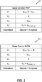
- biasing characteristics e.g., voltages
- the first table 200 may correspond to biasing characteristics as described with respect to the PNP type configuration of the dual mode transistor 100.
- the second table 210 may correspond to biasing characteristics as described with respect to the NPN type configuration of the dual mode transistor 100.
- the first voltage (V 1 ) applied to the first gate region 102 may be biased between ground (e.g., zero volts) and the supply voltage (V dd ).
- the first voltage (V 1 ) may be applied such that a gate-to-source voltage (V GS ) of the dual mode transistor 100 enables channel formation (e.g., formation of a P type inversion layer) within the first body region 108 between the first region 104 and the second region 106.
- a unipolar current (e.g., holes) according to a FET operation may flow from the first region 104 to the second region 106.
- the first voltage (V 1 ) may be adjusted between ground and the supply voltage (V dd ) to adjust (e.g., enlarge) a current gain (beta) of the dual mode transistor 100, a transconductance of the dual mode transistor 100, and a resistance of the dual mode transistor 100 when the second voltage (V 2 ) turns on the horizontal PNP.
- the drain voltage (V d ) applied to the second region 106 may be biased to ground.
- the source voltage (V s ) applied to the first region 104 e.g., the source
- the second voltage (V 2 ) applied to the first terminal 112 may be biased to a voltage that is less than a negative forward junction voltage (e.g., -0.7 V) of the dual mode transistor 100.
- the second voltage (V 2 ) may be less than a difference of the supply voltage (V dd ) applied to the first region 104 and the junction voltage (V j ) (e.g., V 2 ⁇ V dd - V j ). Electrons may flow from the first body region 108 to the first region 104, and holes may flow from the first region 104 to the second region 106.
- a bipolar current e.g., holes and electrons
- unipolar current may be generated.
- the bipolar current may be associated with a BJT operation, and the unipolar current may be associated with a FET operation.
- the first voltage (V 1 ) applied to the first gate region 102 may be biased between the supply voltage (V dd ) and ground (e.g., zero volts).
- the first voltage (V 1 ) may be applied such that a gate-to-source voltage (V GS ) of the dual mode transistor 100 enables channel formation (e.g., formation of an N type inversion layer) within the first body region 108 between the first region 104 and the second region 106.
- a unipolar current (e.g., electrons) according to a FET operation may flow to the first region 104 from the second region 106.
- the first voltage (V1) may be adjusted between ground and the supply voltage (V dd ) to adjust (e.g., enlarge) a current gain (beta) of the dual mode transistor 100, a transconductance of the dual mode transistor 100, and a resistance of the dual mode transistor 100 when the second voltage (V 2 ) turns on the horizontal NPN.
- the drain voltage (V d ) applied to the first region 104 may be biased to the supply voltage (V dd ).
- the source voltage (V s ) applied to the second region 106 may be biased to ground.
- the second voltage (V 2 ) applied to the first terminal 112 (coupled to the first body region 108) may be biased to a voltage that is greater than a forward junction voltage (e.g., 0.7 V) of the dual mode transistor 100.
- the second voltage (V 2 ) may be greater than a difference of the junction voltage (V j ) and the ground voltage applied to the second region 106 (e.g., V 2 > V j ).
- a bipolar current (e.g., holes and electrons) according to a BJT operation may be generated.
- the tables 200, 210 depicted in FIG. 2 include non-limiting examples of biasing characteristics for the dual mode transistor 100 of FIG. 1 .
- the tables 200, 210 illustrate that a unipolar current and a bipolar current may be generated concurrently by biasing the first terminal 112 with the second voltage (V 2 ) such that an absolute value of the body-to-source voltage is greater than a junction voltage (V j ) of the dual mode transistor 100.
- V j junction voltage
- Biasing the first terminal 112 with the second voltage (V 2 ) may enable the dual mode transistor 100 to operate according to a PNP BJT or a NPN BJT.
- Biasing the first gate region 102 with the first voltage (V 1 ) may enable the dual mode transistor 100 to operate according to a FET.
- the dual mode transistor 100 may concurrently operate in a digital MOS mode (e.g., a unipolar operation mode) and an analog gate control BJT mode (e.g., bipolar operation mode).
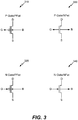
- FIG. 3 particular illustrative embodiments of field effect transistor (FET)-type configurations of a dual mode transistor are shown.
- a first embodiment 310 and a second embodiment 320 illustrate p-type FET (PFET) configurations of a dual mode transistor.
- a third embodiment 330 and a fourth embodiment 340 illustrate n-type FET (NFET) configurations of a dual mode transistor.
- Each embodiment 310-340 may correspond to the dual mode transistor 100 of FIG. 1 .
- the PFET configuration may include a gate that is doped with a P+ concentration or a gate that includes a P-Metal.
- the first embodiment 310 may enable a digital complementary metal oxide semiconductor (CMOS) mode.
- CMOS complementary metal oxide semiconductor
- the first embodiment 310 may enable a unipolar current (e.g., holes) to flow from a source terminal (S) to drain terminal (D).
- the absolute value of a gate-to-source voltage should be larger than an absolute threshold voltage (e.g.,
- V d The drain voltage (V d ) should be grounded, and a source voltage (Vs) should be approximately equal to a supply voltage (V dd ).
- the voltage applied to the body region should be approximately equal to a supply voltage (V dd ).
- the PFET configuration may include a gate that is doped with an N+ concentration or a gate that includes an N-Metal.
- the second embodiment 320 may enable a digital CMOS mode.
- the second embodiment 320 may enable a unipolar current (e.g., holes) to flow from a source terminal (S) to drain terminal (D).
- the absolute value of a gate-to-source voltage should be larger than an absolute threshold voltage (e.g.,
- V d ) should be grounded, and a source voltage (Vs) should be approximately equal to a supply voltage (V dd ).
- the voltage applied to the body region should be approximately equal to a supply voltage (V dd ).
- the NFET configuration may include a gate that is doped with a P+ concentration or a gate that includes a P-Metal.
- the third embodiment 330 may also enable a digital CMOS mode.
- the third embodiment 330 may enable a unipolar current (e.g., electrons) to flow from a source terminal (S) to drain terminal (D).
- the absolute value of a gate-to-source voltage should be larger than an absolute threshold voltage (e.g.,
- V d ) should be approximately equal to a supply voltage (V dd ), and a source voltage (Vs) should be grounded (e.g., zero volts).
- the voltage applied to the body region should be grounded.
- the NFET configuration may include a gate that is doped with an N+ concentration or a gate that includes an N-Metal.
- the fourth embodiment 340 may also enable a digital CMOS mode.
- the fourth embodiment 340 may enable a unipolar current (e.g., electrons) to flow from a source terminal (S) to drain terminal (D).
- the absolute value of a gate-to-source voltage should be larger than an absolute threshold voltage (e.g.,
- V d ) should be approximately equal to a supply voltage (V dd ), and a source voltage (Vs) should be grounded (e.g., zero volts).
- the voltage applied to the body region should be grounded.
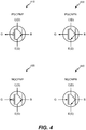
- a first embodiment 410 and a second embodiment 420 illustrate PNP configurations of a dual mode transistor.
- the first embodiment 410 may operate in conjunction with the first embodiment 310 of FIG. 3
- the second embodiment 420 may operate in conjunction with the second embodiment 320 of FIG. 3 .
- a third embodiment 430 and a fourth embodiment 440 illustrate NPN configurations of a dual mode transistor.
- the third embodiment 430 may operate in conjunction with the third embodiment 330 of FIG. 3
- the fourth embodiment 440 may operate in conjunction with the fourth embodiment 340 of FIG. 3 .
- Each embodiment 410-440 may correspond to the dual mode transistor 100 of FIG. 1 .
- the PNP configuration may include a gate that is doped with a P+ concentration or a gate that includes a P-Metal.
- the first embodiment 410 may enable an analog gate control bipolar junction transistor (BJT) mode.
- BJT bipolar junction transistor
- the first embodiment 410 may enable a bipolar current (e.g., holes and electrons).
- holes may flow from an emitter terminal (E) to a collector terminal (C)
- electrons may flow from a base terminal (B) to the emitter terminal (E).
- the gate-to-emitter (source) voltage should be larger than a junction (e.g., threshold) voltage (e.g.,
- the emitter voltage (V e ) should be Vdd, and the collector voltage (V c ) should be approximately equal to ground.
- An absolute value of a base-to-emitter voltage should be larger than a junction threshold (e.g., 0.7 volts) (e.g.,
- the PNP configuration may include a gate that is doped with an N+ concentration or a gate that includes an N-Metal.
- the second embodiment 420 may also enable an analog gate control BJT mode.
- the second embodiment 420 may enable a bipolar current (e.g., holes and electrons).
- holes may flow from an emitter terminal (E) to a collector terminal (C)
- electrons may flow from a base terminal (B) to the emitter terminal (E).
- the gate-to-emitter (source) voltage should be larger than a junction (e.g., threshold) voltage (e.g.,
- the emitter voltage (V e ) should be Vdd, and the collector voltage (V c ) should be approximately equal to ground.
- An absolute value of a base-to-emitter voltage should be larger than a junction threshold (e.g., 0.7 volts) (e.g.,
- the NPN configuration may include a gate that is doped with a P+ concentration or a gate that includes a P-Metal.
- the third embodiment 430 may also enable an analog gate control BJT mode.
- the third embodiment 430 may enable a bipolar current (e.g., holes and electrons).
- holes may flow from a base terminal (B) to an emitter terminal (E), and electrons may flow from the emitter terminal (E) to a collector terminal (C).
- the gate-to-emitter (source) voltage should be larger than a junction (e.g., threshold) voltage (e.g., V g - V e > Vt).
- the emitter voltage (V e ) should be approximately equal to ground, and the collector voltage (V c ) should be Vdd.
- An absolute value of a base-to-emitter voltage should be larger than a junction threshold (e.g., 0.7 volts) (e.g.,
- the NPN configuration may include a gate that is doped with an N+ concentration or a gate that includes an N-Metal.
- the fourth embodiment 440 may also enable an analog gate control BJT mode.
- the fourth embodiment 440 may enable a bipolar current (e.g., holes and electrons).
- holes may flow from a base terminal (B) to an emitter terminal (E), and electrons may flow from the emitter terminal (E) to a collector terminal (C).
- the gate-to-emitter (source) voltage should be larger than a junction (e.g., threshold) voltage (e.g., V g - V e > Vt).
- the emitter voltage (V e ) should be approximately equal to ground, and the collector voltage (V c ) should be Vdd.
- An absolute value of a base-to-emitter voltage should be larger than a junction threshold (e.g., 0.7 volts) (e.g.,
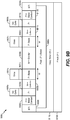
- FIG. 5 particular illustrative embodiments 510, 520 of an inverter mixer that includes dual mode transistors are shown.
- a first embodiment 510 of the inverter mixer includes a first dual mode transistor 512 and a second dual mode transistor 514.
- the first dual mode transistor 512 and the second dual mode transistor 514 may each correspond to the dual mode transistor 100 of FIG. 1 .
- the first dual mode transistor 512 and the second dual mode transistor 514 may each correspond to any of the embodiments 310-340 of FIG. 3 and the corresponding embodiments 410-440 of FIG. 4 .
- a first body region of the first dual mode transistor 512 may be coupled to a second body region of the second dual mode transistor 514.
- the first body region and the second body region may also be coupled to receive a first input signal 516.
- the first input signal 516 may correspond to a local oscillator (LO) signal.
- a first gate of the first dual mode transistor 512 may be coupled to a second gate of the second dual mode transistor 514.
- the first gate and the second gate may also be coupled to receive a second input signal 518.
- the second input signal 518 may correspond to a radio frequency (RF) signal.
- RF radio frequency
- a first source (e.g., a first emitter) of the first dual mode transistor 512 may be coupled to receive a supply voltage (V dd ), and a second source (e.g., a second emitter) of the second dual mode transistor 514 may be coupled to ground (V ss ).
- a first drain (e.g., a first collector) of the first dual mode transistor 512 may be coupled to a second drain (e.g., a second collector) of the second dual mode transistor 514.
- the first drain and the second drain may generate an output signal 519.
- the output signal 519 may correspond to a sum of the RF signal and the LO signal.
- the first dual mode transistor 512 may be a PMOS (PNP) transistor, and the second dual mode transistor 514 may be an NMOS (NPN) transistor.
- the first embodiment 510 may invert the second input signal 518 (e.g., the RF signal) and mix the inverted second input signal with the first input signal 516 (e.g., the LO signal) applied to the first body region. For example, when the second input signal 518 has a logic low voltage level, the first dual mode transistor 512 may be activated and a RF signal (e.g., 518) is inverted from the second input signal 518 to output 519 according to concurrent bipolar and unipolar operation, as described above.
- a RF signal e.g., 518
- the logic low voltage level of the second input signal 518 may enable a unipolar current (e.g., holes) to flow from the first source to the first drain and tuned by the second input signal 518, and the first input signal 516 (having a logic voltage level that is less than a negative forward junction voltage (V j ) of the first dual mode transistor 512) may enable a bipolar current to flow and tuned by the first input signal 516.
- a unipolar current e.g., holes
- V j negative forward junction voltage
- the second dual mode transistor 514 may be activated and a RF signal (e.g., 518) is inverted from the second input signal 518 to output 519 according to concurrent bipolar and unipolar operation, as described above.
- a RF signal e.g., 518
- the logic high voltage level of the second input signal 518 may enable a unipolar current (e.g., electrons) to flow from the second source to the second drain and tuned by the second input signal 518
- the first input signal 516 (having a logic voltage level that is greater than a forward junction voltage (V j ) of the second dual mode transistor 514) may enable a bipolar current to flow and tuned by the first input signal 516.
- a second embodiment 520 of the inverter mixer includes a first dual mode transistor 522 and a second dual mode transistor 524.
- the first dual mode transistor 522 and the second dual mode transistor 524 may each correspond to the dual mode transistor 100 of FIG. 1 .
- the first dual mode transistor 522 and the second dual mode transistor 524 may each correspond to any of the embodiments 310-340 of FIG. 3 and the corresponding embodiments 410-440 of FIG. 4 .
- a first body region of the first dual mode transistor 522 may be coupled to receive a first input signal 516.
- the first input signal 526 may be a first LO signal having a voltage ranging approximately from a relatively high range (e.g., 0.4 V to 1.5 V).
- a second body region of the second dual mode transistor 524 may be coupled to receive a second input signal 527.
- the second input signal 527 may be a second LO signal having a voltage ranging approximately from a relatively low range (e.g., 0 V to 1.2 V).
- a first gate of the first dual mode transistor 522 may be coupled to a second gate of the second dual mode transistor 524.
- the first gate and the second gate may also be coupled to receive a third input signal 528.
- the third input signal 528 may correspond to an RF signal.
- a first source (e.g., a first emitter) of the first dual mode transistor 522 may be coupled to receive a supply voltage (V dd ), and a second source (e.g., a second emitter) of the second dual mode transistor 524 may be coupled to ground (V ss ).
- a first drain (e.g., a first collector) of first dual mode transistor 522 may be coupled to a second drain (e.g., a second collector) of the second dual mode transistor 524.
- the first drain and the second drain may generate an output signal 529.
- the output signal 529 may correspond to a sum of the RF signal and the LO signals.
- the first dual mode transistor 522 may be a PMOS (PNP) transistor, and the second dual mode transistor 524 may be an NMOS (NPN) transistor.
- the second embodiment 520 may invert the third input signal 528 (e.g., the RF signal) and mix the inverted third input signal with the first input signal 526 (e.g., the LO signal) applied to the first body region (and/or with the second input signal 527 applied to the second body region).
- the third input signal 528 has a logic low voltage level
- the first dual mode transistor 522 may be activated and a RF signal (e.g., 528) is inverted from the third input signal 528 to output signal 529 according to concurrent bipolar and unipolar operation, as described above.
- the logic low voltage level of the third input signal 528 may enable a unipolar current (e.g., holes) to flow from the first source to the first drain and tuned by the third input signal 528, and the first input signal 526 (having a logic voltage level that is less than a negative forward junction voltage (V j ) of the first dual mode transistor 522) may enable a bipolar current to flow and tuned by the first input signal 526.
- a unipolar current e.g., holes
- V j negative forward junction voltage
- the second dual mode transistor 524 may be activated and a RF signal (e.g., 528) is inverted from the third input signal 528 to output signal 529 according to concurrent bipolar and unipolar operation, as described above.
- a RF signal e.g., 528
- the logic high voltage level of the third input signal 528 may enable a unipolar current (e.g., electrons) to flow from the second source to the second drain and tuned by the third input signal 528
- the second input signal 527 (having a logic voltage level that is greater than a forward junction voltage (V j ) of the second dual mode transistor 524) may enable a bipolar current to flow and tuned by the second input signal 527.
- the differential mixer 600 includes a first dual mode transistor 602 and a second dual mode transistor 604.
- the first dual mode transistor 602 and the second dual mode transistor 604 may each correspond to the dual mode transistor 100 of FIG. 1 .
- the first dual mode transistor 602 and the second dual mode transistor 604 may each correspond to any of the embodiments 310-340 of FIG. 3 and the corresponding embodiments 410-440 of FIG. 4 .
- a first gate of the first dual mode transistor 602 may be coupled to receive a first signal of a first differential signal.
- the first differential signal may be a radio frequency (RF) signal.
- a second gate of the second dual mode transistor 604 may be coupled to receive a second (e.g., complementary) signal of the first differential signal.
- a first body region of the first dual mode transistor 602 may be coupled to receive a second signal of a second differential signal.
- the second differential signal may be a local oscillator (LO) signal.
- a second body region of the second dual mode transistor 604 may be coupled to receive a first (e.g., complementary) signal of the second differential signal.
- a first source (e.g., a first emitter) of the first dual mode transistor 602 may be coupled to a second source (e.g., a second emitter) of the second dual mode transistor 604.
- the first drain and the second drain may generate a differential output signal.
- the output signal may be an intermediate frequency signal.
- the differential mixer 600 of FIG. 6 may include two dual mode transistors 602, 604 that are differentially driven.
- the differential mixer 600 may enable a relatively high native small-signal gain from NMOS and BJT modulation, which may lead to a relatively high conversion gain. Due to a single-stage operation and the relatively high conversion gain, the differential mixer 600 may generate less noise and better gain and linearity than a conventional Gilbert differential mixer (not shown).
- the (two transistor) dual mode differential mixer 600 reduces stages from two to one and improves delay, power efficiency and gain.
- the differential mixer 600 has two dual mode transistors and one stage in comparison with the six traditional transistors and two stages of the Gilbert differential mixer.
- the differential mixer 600 may also operate in a lower power mode and may enable single direct-current (DC) bias for mixing operations.
- DC direct-current
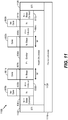
- a first embodiment 710 of the inverter driver includes a first dual mode transistor 712 and a second dual mode transistor 714.
- first dual mode transistor 712 and the second dual mode transistor 714 may each correspond to the dual mode transistor 100 of FIG. 1 .
- the first dual mode transistor 712 and the second dual mode transistor 714 may each correspond to any of the embodiments 310-340 of FIG. 3 and the corresponding embodiments 410-440 of FIG. 4 .
- a first body region of the first dual mode transistor 712 may be coupled to a second body region of the second dual mode transistor 714.
- the first body region and the second body region may also be coupled to receive a first input signal 716.
- a first gate of the first dual mode transistor 712 may be coupled to a second gate of the second dual mode transistor 714.
- the first gate and the second gate may also be coupled to receive the first input signal 516.
- a first source (e.g., a first emitter) of the first dual mode transistor 712 may be coupled to receive a supply voltage (V dd ), and a second source (e.g., a second emitter) of the second dual mode transistor 714 may be coupled to ground (V ss ).
- a first drain (e.g., a first collector) of first dual mode transistor 712 may be coupled to a second drain (e.g., a second collector) of the second dual mode transistor 714. The first drain and the second drain may generate an output signal 719.
- the first dual mode transistor 712 may be a PMOS (PNP) transistor, and the second dual mode transistor 714 may be an NMOS (NPN) transistor.
- the first embodiment 710 may invert the first input signal 716 and drive the inverted first input signal to an output. For example, when the first input signal 716 has a logic low voltage level, the first dual mode transistor 712 may be activated and a logic low voltage level signal (e.g., 716) is inverted from the first input signal 716 to the output signal 719 according to concurrent bipolar and unipolar operation, as described above.
- a logic low voltage level signal e.g., 716
- the logic low voltage level of the first input signal 716 may enable a unipolar current (e.g., holes) to flow from the first source to the first drain and tuned by the first input signal 716.
- the low voltage level of the first input signal 716 may be less than a negative forward junction voltage (Vj) of the first dual mode transistor 712, enabling a bipolar current to flow when applied to the first body region and tuned by the first input signal 716.
- the second dual mode transistor 714 may be activated and a logic high voltage level signal (e.g., 716) is inverted from the first input signal 716 to the output signal 719 according to concurrent bipolar and unipolar operation, as described above.
- a logic high voltage level of the first input signal 716 may enable a unipolar current (e.g., electrons) to flow from the second source to the second drain and tuned by the first input signal 716.
- the high voltage level of the first input signal 716 may be greater than a forward junction voltage (V j ) of the second dual mode transistor 714, enabling a bipolar current to flow when applied to the first body region and tuned by the first input signal 716.
- a second embodiment 720 of the inverter driver includes a first dual mode transistor 722 and a second dual mode transistor 724.
- the first dual mode transistor 722 and the second dual mode transistor 724 may each correspond to the dual mode transistor 100 of FIG. 1 .
- the first dual mode transistor 722 and the second dual mode transistor 724 may each correspond to any of the embodiments 310-340 of FIG. 3 and the corresponding embodiments 410-440 of FIG. 4 .
- a first body region of the first dual mode transistor 722 may be coupled to receive a first input signal 726.
- a first gate of the first dual mode transistor 722 may be coupled to a second gate of the second dual mode transistor 724.
- the first gate and the second gate may also be coupled to receive a second input signal 727.
- a second body region of the second dual mode transistor 724 may be coupled to receive a third input signal 728.
- a first source (e.g., a first emitter) of the first dual mode transistor 722 may be coupled to receive a supply voltage (V dd ), and a second source (e.g., a second emitter) of the second dual mode transistor 724 may be coupled to ground (V ss ).
- a first drain (e.g., a first collector) of first dual mode transistor 722 may be coupled to a second drain (e.g., a second collector) of the second dual mode transistor 724. The first drain and the second drain may generate an output signal 729.
- the first dual mode transistor 722 may be a PMOS (PNP) transistor, and the second dual mode transistor 724 may be an NMOS (NPN) transistor.
- the second embodiment 720 may invert the second input signal 727 and drive the inverted second input signal to an output. For example, when the second input signal 727 has a logic low voltage level, the first dual mode transistor 722 may be activated and a logic low voltage level signal (e.g., 727) is inverted from the second input signal 727 to the output signal 729 according to concurrent bipolar and unipolar operation, as described above.
- the logic low voltage level of the second input signal 727 may enable a unipolar current (e.g., holes) to flow from the first source to the first drain and tuned by the second input signal 727.
- the first input signal 726 may have a logic low voltage level that is less than a negative forward junction voltage (Vj) of the first dual mode transistor 722, enabling a bipolar current to flow when applied to the first body region and tuned by the first input signal
- the second dual mode transistor 724 may be activated and a logic high voltage level signal (e.g., 727) is inverted from the second input signal 727 to the output signal 729 according to concurrent bipolar and unipolar operation, as described above.
- a logic high voltage level of the second input signal 727 may enable a unipolar current (e.g., electrons) to flow from the second source to the second drain.
- the third input signal 728 may have a logic high voltage level that is greater than a forward junction voltage (V j ) of the second dual mode transistor 724, enabling a bipolar current to flow when applied to the first body region and tuned by the third input signal 728.
- FIG. 8a a particular illustrative embodiment of a PNP dual mode transistor 800a is shown.
- the PNP dual mode transistor 800a may correspond to the dual mode transistor 100 of FIG. 1 .
- the PNP dual mode transistor 800a includes a first N- base region 807a and a second N- base region 808a. Each N- base region 807a, 808a may have a particular width (W).
- the first N- base region 807a and the second N- base region 808a may be coupled to (or include) an N- base well 809a.
- An N++ base contact 812a, 836a may also be coupled to the N- base regions 807a, 808a via the N- base well 809a.
- the N++ base contact 812a, 836a may correspond to the first terminal 112 of FIG. 1 .
- the PNP dual mode transistor 800a also includes an emitter region 806a, a first collector region 804a, and a second collector region 832a.
- the emitter region 806a, the first collector region 804a, and the second collector region 832a may each be doped with a P++ concentration.
- a first STI area 822a may prevent (or reduce) current leakage (from N++ base to P++ collector) from affecting the PNP dual mode transistor 800a.
- a second STI area 826a may prevent (or reduce) current leakage between the first collector region 804a and the N++ base contact 812a.
- a first gate 801a may be coupled to the first N- base region 807a via a dielectric layer, and a second gate 802a may be coupled to the second N- base region 808a via a dielectric layer.
- a current gain of the PNP dual mode transistor 800a may be controlled by a gate voltage applied to the gates 801a, 802a.
- the PNP dual mode transistor 800a may also include a P- substrate 810a.
- the PNP dual mode transistor 800a may operate in a digital MOS mode (e.g., a unipolar operation mode) and an analog gate control BJT mode (e.g., bipolar operation mode).
- the gate voltages may be biased so that a gate-source-voltage enables formation of an inversion layer within the second N- base region 808a.
- a unipolar current e.g., holes
- the N++ base contact 812a, 836a may be biased such that an absolute value of a voltage difference between the N- base well 809a and the first collector region 804a, second collector region 832a is greater than a forward junction voltage (Vj) of the PNP dual mode transistor 800a.
- Vj forward junction voltage
- the N++ base contact may be biased to a voltage that is less than a negative forward junction voltage (e.g., -0.7 V) of the PNP dual mode transistor 800a. Biasing the N++ base contact may enable the PNP dual mode transistor 800a to operate according to a PNP BJT (e.g., generate a bipolar current including holes and electrons).
- a particular illustrative embodiment of a PNP dual mode transistor 800b is shown.
- the PNP dual mode transistor 800b may correspond to the dual mode transistor 100 of FIG. 1 .
- the PNP dual mode transistor 800b includes a first N- base region 807b and a second N- base region 808b. Each N- base region 807b, 808b may have a particular width (W).
- the first N- base region 807b and the second N- base region 808b may be coupled to (or include) an N- base well 809b.
- An N++ base contact 812b, 836b may also be coupled to the N- base regions 807b, 808b via the N- base well 809b.
- the N++ base contact 812b, 836b may correspond to the first terminal 112 of FIG. 1 .
- the PNP dual mode transistor 800b also includes an emitter region 806b, a first collector region 804b, and a second collector region 832b.
- the emitter region 806b, the first collector region 804b, and the second collector region 832b may each be doped with a P++ concentration.
- a first STI area 822b may prevent (or reduce) current leakage (from other transistors) from affecting the PNP dual mode transistor 800b.
- a second STI area 826b may prevent (or reduce) current leakage from other transistors.
- a first gate 801b may be coupled to the first N- base region 807b via a dielectric layer, and a second gate 802b may be coupled to the second N- base region 808b via a dielectric layer.
- Isolate gates 803b, 805b may be coupled to the third and fourth N- base region 811b, 835b via a dielectric layer.
- the isolate gates 803b, 805b may be used to isolate N++ base contact from P++ collector.
- a current gain of the PNP dual mode transistor 800b may be controlled by a gate voltage applied to the gates 801b, 802b.
- the PNP dual mode transistor 800b may also include a P- substrate 810b.
- the PNP dual mode transistor 800b may operate in a digital MOS mode (e.g., a unipolar operation mode) and an analog gate control BJT mode (e.g., bipolar operation mode).
- the gate voltages may be biased so that a gate-source-voltage enables formation of an inversion layer within the first and second N- base region 807b, 808b.
- a unipolar current e.g., holes
- the N++ base contact 812b, 836b may be biased such that an absolute value of a voltage difference between the N- base well 809b and the first collector region 804b, second collector region 832b is greater than a forward junction voltage (Vj) of the PNP dual mode transistor 800b.
- Vj forward junction voltage
- the N++ base contact may be biased to a voltage that is less than a negative forward junction voltage (e.g., -0.7 V) of the PNP dual mode transistor 800b. Biasing the N++ base contact may enable the PNP dual mode transistor 800b to operate according to a PNP BJT (e.g., generate a bipolar current including holes and electrons).
- NPN dual mode transistor 900a a particular illustrative embodiment of an NPN dual mode transistor 900a is shown.
- the NPN dual mode transistor 900a may correspond to the dual mode transistor 100 of FIG. 1 .
- the NPN dual mode transistor 900a includes a first p- base region 907a and a second P- base region 908a. Each P- base region 907a, 908a may have a particular width (W).
- the first P- base region 907a and the second P- base region 908a may be coupled to (or include) a P- base well 909a.
- a P++ base contact 912a, 936a may also be coupled to the P- base regions 907a, 908a via the P- base well 909a.
- the P++ base contact 912a, 936a may correspond to the first terminal 112 of FIG. 1 .
- the NPN dual mode transistor 900a also includes an emitter region 906a, a first collector region 904a, and a second collector region 932a.
- the emitter region 906a, the first collector region 904a, and the second collector region 932a may each be doped with an N++ concentration.
- a first STI area 922a may prevent (or reduce) current leakage (from P++ base contact 936a).
- a second STI area 926a may prevent (or reduce) current leakage between the first collector region 904a and the P++ base contact 912a.
- a first gate 901a may be coupled to the first P- base region 907a via a dielectric layer, and a second gate 902a may be coupled to the second P- base region 907a via a dielectric layer.
- a current gain of the NPN dual mode transistor 900a may be controlled by a gate voltage applied to the gates 901a, 902a.
- the NPN dual mode transistor 900a may also include a P- base well 910a and an N- base well 911a.
- the NPN dual mode transistor 900a may operate in a digital MOS mode (e.g., a unipolar operation mode) and an analog gate control BJT mode (e.g., bipolar operation mode).
- the gate voltages may be biased so that a gate-source-voltage enables formation of an inversion layer within the first and second N- base regions 907a and 908a.
- a unipolar current e.g., electrons
- the P++ base contact 912a and 936a may be biased such that an absolute value of a voltage difference between the P- base well 909a and the first and second collector regions 932a,904a is greater than the junction voltage (V j ) of the NPN dual mode transistor 900a. Biasing the P++ base contact may enable the NPN dual mode transistor 900a to operate according to a NPN BJT (e.g., generate a bipolar current including holes and electrons).
- NPN dual mode transistor 900b may correspond to the dual mode transistor 100 of FIG. 1 .
- the NPN dual mode transistor 900b includes a first p- base region 907b and a second P- base region 908b. Each P- base region 907b, 908b may have a particular width (W).
- the first P- base region 907b and the second P- base region 908b may be coupled to (or include) a P- base well 909b.
- a P++ base contact 912b and 936b may also be coupled to the P- base regions 907b, 908b via the P- base well 909b.
- the P++ base contact 912b and 936b may correspond to the first terminal 112 of FIG. 1 .
- the NPN dual mode transistor 900b also includes an emitter region 906b, a first collector region 904b, and a second collector region 932b.
- the emitter region 906b, the first collector region 904b, and the second collector region 932b may each be doped with an N++ concentration.
- a first STI area 922b may prevent (or reduce) current leakage (from P++ base contact 936b).
- a second STI area 926b may prevent (or reduce) current leakage between the first collector region 904b and the P++ base contact 912b.
- a first gate 901b may be coupled to the first P- base region 907b via a dielectric layer, and a second gate 902b may be coupled to the second P- base region 907b via a dielectric layer.
- Isolate gates 903b, 905b may be coupled to the third and fourth N- base region 911b, 935b via a dielectric layer.
- the isolate gates 903b, 905b used to isolate N++ base contact from P++ collector.
- a current gain of the NPN dual mode transistor 900b may be controlled by a gate voltage applied to the gates 901b, 902b.
- the NPN dual mode transistor 900b may also include a P- base well 910b and an N- base well 911b.
- the NPN dual mode transistor 900b may operate in a digital MOS mode (e.g., a unipolar operation mode) and an analog gate control BJT mode (e.g., bipolar operation mode).
- the gate voltages may be biased so that a gate-source-voltage enables formation of an inversion layer within the first and second N- base regions 907b and 908b.
- a unipolar current e.g., electrons
- the P++ base contact 912b and 936b may be biased such that an absolute value of a voltage difference between the P- base well 909b and the first and second collector region 932b and 904b is greater than the junction voltage (V j ) of the NPN dual mode transistor 900b. Biasing the P++ base contact may enable the NPN dual mode transistor 900b to operate according to a NPN BJT (e.g., generate a bipolar current including holes and electrons).
- FIG. 10a a particular illustrative chart 1000-la depicting a change in drain current of a dual mode transistor based on biasing characteristics is shown. Values and results depicted in the chart 1000-la are provided for illustrative purposes and should not be construed as limiting. Values may vary based on external conditions (e.g., temperature), gate widths of the dual mode transistor, gate lengths of the dual mode transistors, doping concentrations associated with the dual mode transistor, biasing voltages, etc.
- the chart 1000-la illustrates operating results that correspond to an NPN-type configuration of the dual mode transistor 100 of FIG. 1 .
- the second voltage (V 2 ) applied to the first terminal 112 may correspond to the base voltage (V B ) depicted in the chart 1000.
- the first voltage (V 1 ) applied to the first gate region 102 of FIG. 1 may be approximately 1.5 V, as depicted in the chart 1000-la.
- the chart 1000-la illustrates that a drain current (e.g., a collector current) may increase as the base voltage (V B ) increases for a particular drain voltage.
- the drain current may be approximately 540 uA/um when a 0.8 V signal is applied to the first terminal 112 and a 1.5 V signal is applied to the drain.
- the drain current may be reduced to approximately 240 uA/um.
- the drain current increases when both the unipolar operation (e.g., the FET operation) associated with unipolar current and the bipolar operation (e.g., the BJT operation) associated with the bipolar current are active as opposed to when only a single operation (e.g., unipolar or bipolar) is active.
- the base voltage (V B ) is 0.2 V (e.g., when the bipolar operation is inactive and the unipolar operation is active) the drain current is approximately 450 uA/um when a 1.5 voltage signal is applied to the drain.
- the base voltage (V B ) is 1.2 V (e.g., when the bipolar operation and the unipolar operation are active)
- the drain current increases to approximately 650 uA/um when the 1.5 voltage signal is applied to the drain.
- FIG.1 Another particular illustrative chart 1000-2a depicts the first gate region 102 controlling drain current at different the first terminal 112 (base) voltage of FIG.1 .
- the base voltage between 0.6V ⁇ 1.2V has higher NPN efficiency.
- FIG. 10b a particular illustrative chart 1000-lb depicting a change in current gain (beta) of a dual mode transistor based on biasing characteristics of the first gate region 102 and the first terminal 112 voltage of FIG.1 is shown.
- an NPN activated region e.g., where the first terminal voltage of FIG. 1 is 0.6V-1.2V
- the current gain (beta) of the NPN is controlled by the first gate region voltage 102 and the first terminal region 112 voltage of FIG.1 .
- FIG. 1000-2b Another particular illustrative chart 1000-2b depicting a change in transconductance (gm) of a dual mode transistor based on biasing characteristics of the first gate region 102 and the first terminal 112 voltage of FIG.1 is shown.
- an NPN activated region e.g., where the first terminal voltage of FIG. 1 is 0.6V ⁇ 1.2V
- the transconductance (gm) of the NPN is controlled by the first gate region voltage 102 and the first terminal region 112 voltage of FIG.1 .
- the SOI PNP dual mode transistor 1100 may correspond to the dual mode transistor 100 of FIG. 1 .
- the SOI PNP dual mode transistor 1100 may include a similar configuration as the PNP dual mode transistor 800b of FIG. 8b ; however, STIs 1122, 1126 may be extended through an Nwell base 1109 and may be coupled with an oxide substrate 1110.
- the oxide substrate 1110 may be different from the P- substrate 810b of FIG. 8b .
- the SOI PNP dual mode transistor 1100 may have a PMOS/PNP silicon-on-insulator configuration and the PNP dual mode transistor 800b of FIG. 8b may have a PMOS/PNP bulk silicon configuration.
- the SOI NPN dual mode transistor 1200 may correspond to the dual mode transistor 100 of FIG. 1 .
- the SOI NPN dual mode transistor 1200 may include a similar configuration as the NPN dual mode transistor 900b of FIG. 9b ; however, STIs 1222, 1226 may be extended through a Pwell base 1209 and may be coupled with an oxide substrate 1210.
- the oxide substrate 1210 may be different from the P- base well 910b and the N- base well 911b.
- the SOI NPN dual mode transistor 1200 may have a NMOS/NPN silicon-on-insulator configuration and the NPN dual mode transistor 900b of FIG. 9b may have a NMOS/NPN bulk silicon configuration.
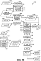
- the method 1300 may be performed with respect to the dual mode transistor 100 of FIG. 1 , at least one of the embodiments 310-340 of the FET-type configurations of FIG. 3 , at least one of the embodiments 410-440 of the BJT-type configurations of FIG. 4 , at least one of the embodiments 510, 520 of the inverter mixer of FIG. 5 , the differential mixer 600 of FIG. 6 , at least one of the embodiments 710, 720 of the inverter driver of FIG. 7 , the PNP dual mode transistors 800a, 800b of FIG.
- the NPN dual mode transistors 900a, 900b of FIG. 9a and 9b the NPN dual mode transistors 900a, 900b of FIG. 9a and 9b , the SOI PNP dual mode transistor 1100 of FIG. 11 , the SOI NPN dual mode transistor 1200 of FIG. 12 , or any combination thereof.
- the method 1100 includes biasing a first gate voltage to enable unipolar current to flow from a first region of a transistor to a second region of the transistor according to a FET-type operation, at 1302.
- the first gate voltage of the first gate region 102 may be biased to a first voltage (V 1 ).
- Biasing the first gate voltage may enable unipolar current to flow from the first region 104 to the second region 106 according to a FET-type operation.
- the source voltage (V s ) may be applied to the first region 104.
- the first gate region 102 may be biased such that the first voltage (V 1 ) is lower than the source voltage (V s ).
- the supply voltage (V dd ) may be applied to the first region 104 (e.g., the source), and the first voltage (V 1 ) may range from ground (e.g., zero volts) to the supply voltage (V dd ) such that the gate voltage is lower than the source voltage (V s ).
- Biasing the first gate region 102 with the first voltage (V 1 ) may enable channel formation (e.g., formation of an inversion layer) within the first body region 108 between the first region 104 and the second region 106.
- the unipolar current (e.g., holes) according to a PFET operation may flow from the first region 104 to the second region 106.
- the first gate region 102 may be biased such that the first voltage (V 1 ) is greater than a source voltage.
- a ground voltage e.g., zero volts
- the second region 106 e.g., the source
- the first voltage (V 1 ) may range from ground to the supply voltage (V dd ) such that the first voltage (V 1 ) is greater than the source voltage.
- Biasing the first gate region 102 with the first voltage (V 1 ) may enable channel formation (e.g., formation of an inversion layer) within the first body region 108 between the first region 104 and the second region 106.
- the unipolar current e.g., electrons
- an NFET operation may flow from the first region 104 to the second region 106.
- a body terminal may be biased to enable bipolar current to flow from the first region to the second region according to a BJT-type operation, at 1304.
- the first terminal 112 (coupled to the first body region 108) may be biased to the second voltage (V 2 ).
- the first terminal 112 may be biased such that an absolute value of a body-to-source voltage (e.g., a voltage difference between the second voltage (V 2 ) and the source voltage (V s )) is greater than a junction voltage (Vj) of the dual mode transistor 100. Biasing the first terminal 112 may enable bipolar current to flow between the first region 104 and the second region 106 concurrently with the unipolar current.
- the second voltage (V 2 ) applied to the first terminal 112 (coupled to the first body region 108) may be biased to a voltage that is less than a negative forward junction voltage (e.g., -0.7 V) of the dual mode transistor 100.
- the second voltage (V 2 ) applied to the first terminal 112 (coupled to the first body region 108) may be biased to a voltage that is greater than a forward junction voltage (e.g., 0.7 V) of the dual mode transistor 100.
- a bipolar current (including electrons and holes) according to a BJT-type operation may flow between the first region 104 and the second region 106 in response to biasing the first terminal 112 to the second voltage (V 2 ).
- the method 1300 of FIG. 13 may enable a concurrent digital MOS operation mode (e.g., a unipolar operation mode corresponding to a unipolar current) and an analog gate control BJT operation mode (e.g., bipolar operation mode corresponding to a bipolar current).
- a concurrent digital MOS operation mode e.g., a unipolar operation mode corresponding to a unipolar current
- an analog gate control BJT operation mode e.g., bipolar operation mode corresponding to a bipolar current.
- V dd supply voltage
- the dual mode transistor enables the gate control BJT operation and provides high performance BJT transistor in logic CMOS process.
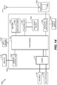
- the device 1400 includes a processor 1410, such as a digital signal processor (DSP), coupled to a memory 1432.
- DSP digital signal processor
- FIG. 14 also shows a display controller 1426 that is coupled to the processor 1410 and to a display 1428.
- a coder/decoder (CODEC) 1434 can also be coupled to the processor 1410.
- a speaker 1436 and a microphone 1438 can be coupled to the CODEC 1434.
- FIG. 14 also indicates that a wireless controller 1440 can be coupled to the processor 1410 and to an antenna 1442 via a radio-frequency (RF) interface 1490 disposed between the wireless controller 1440 and the antenna 1442.
- the RF interface 1490 may include a dual mode transistor device 1460 (or a component that includes one or more dual mode transistor devices).
- the dual mode transistor device 1460 may include, or correspond to, the dual mode transistor 100 of FIG.
- a controller 1402 may also be coupled to the processor 1410 and to a dual mode transistor device 1450 (or a component that includes one or more dual mode transistor devices).
- the dual mode transistor device 1450 may include, or correspond to, the dual mode transistor 100 of FIG. 1 , at least one of the embodiments 310-340 of the FET-type configurations of FIG. 3 , at least one of the embodiments 410-440 of the BJT-type configurations of FIG. 4 , at least one of the embodiments 510, 520 of the inverter mixer of FIG. 5 , the differential mixer 600 of FIG. 6 , at least one of the embodiments 710, 720 of the inverter driver of FIG. 7 , the PNP dual mode transistor 800a, 800b of FIG.
- the controller 1402 may be a hardware controller, a firmware, or a combination thereof.
- the memory 1432 may be a tangible non-transitory processor-readable storage medium that includes executable instructions 1456.
- the instructions 1456 may be executed by a processor, such as the controller 1402, to perform the method 1300 of FIG. 13 .
- the instructions 1456 may be executable by the controller 1402 to bias the gate of the dual mode transistor device 1450 and/or the dual mode transistor device 1460.
- the instructions 1456 may also be executable by the controller 1402 to bias the terminal coupled to a body region of the dual mode transistor device 1450 and/or the dual mode transistor device 1460.
- the instructions 1456 may also be executable by an alternative processor (not shown) coupled to the processor 1410.
- the processor 1410, the display controller 1426, the memory 1432, the CODEC 1434, and the wireless controller 1440 are included in a system-in-package or system-on-chip device 1422.
- an input device 1430 and a power supply 1444 are coupled to the system-on-chip device 1422.
- the display 1428, the input device 1430, the speaker 1436, the microphone 1438, the antenna 1442, and the power supply 1444 are external to the system-on-chip device 1422.
- each of the display 1428, the input device 1430, the speaker 1436, the microphone 1438, the antenna 1442, and the power supply 1444 can be coupled to a component of the system-on-chip device 1422, such as an interface or a controller.
- an apparatus includes means for biasing a first gate voltage to enable unipolar current to flow from a first region of a transistor to a second region of the transistor according to a FET-type operation.
- the means for biasing the first gate voltage may include the controller 1402 operable to execute the instructions 1462 of FIG. 14 , one or more other devices, circuits, modules, or any combination thereof.
- the apparatus may also include means for biasing a body terminal to enable bipolar current to flow from the first region to the second region according to a BJT-type operation.
- the unipolar current may flow concurrently with the bipolar current.
- the means for biasing the body terminal may include the controller 1402 operable to execute the instructions 1462 of FIG. 14 , one or more other devices, circuits, modules, or any combination thereof.
- FIG. 13 depicts a particular illustrative embodiment of an electronic device manufacturing process 1300.
- Physical device information 1302 is received at the manufacturing process 1300, such as at a research computer 1306.
- the physical device information 1302 may include design information representing at least one physical property of a semiconductor device, such as a device that includes the dual mode transistor 100 of FIG. 1 , at least one of the embodiments 310-340 of the FET-type configurations of FIG. 3 , at least one of the embodiments 410-440 of the BJT-type configurations of FIG. 4 , at least one of the embodiments 510, 520 of the inverter mixer of FIG. 5 , the differential mixer 600 of FIG. 6 , at least one of the embodiments 710, 720 of the inverter driver of FIG. 7 , the PNP dual mode transistor 800a, 800b of FIG.
- the physical device information 1502 may include physical parameters, material characteristics, and structure information that is entered via a user interface 1504 coupled to the research computer 1506.
- the research computer 1506 includes a processor 1508, such as one or more processing cores, coupled to a computer readable medium such as a memory 1510.
- the memory 1510 may store computer readable instructions that are executable to cause the processor 1508 to transform the physical device information 1502 to comply with a file format and to generate a library file 1512.
- the library file 1512 includes at least one data file including the transformed design information.
- the library file 1512 may include a library of semiconductor devices including the dual mode transistor 100 of FIG. 1 , at least one of the embodiments 310-340 of the FET-type configurations of FIG. 3 , at least one of the embodiments 410-440 of the BJT-type configurations of FIG. 4 , at least one of the embodiments 510, 520 of the inverter mixer of FIG. 5 , the differential mixer 600 of FIG. 6 , at least one of the embodiments 710, 720 of the inverter driver of FIG. 7 , the PNP dual mode transistor 800a, 800b of FIG.
- the NPN dual mode transistor 900a, 900b of FIG. 9a and 9b the NPN dual mode transistor 900a, 900b of FIG. 9a and 9b , the SOI PNP dual mode transistor 1100 of FIG. 11 , the SOI NPN dual mode transistor 1200 of FIG. 12 , the dual mode transistor device 1450 of FIG. 14 , the dual mode transistor device 1460 of FIG. 14 , or any combination thereof, that is provided for use with an electronic design automation (EDA) tool 1520.
- EDA electronic design automation
- the library file 1512 may be used in conjunction with the EDA tool 1520 at a design computer 1514 including a processor 1516, such as one or more processing cores, coupled to a memory 1518.
- the EDA tool 1520 may be stored as processor executable instructions at the memory 1518 to enable a user of the design computer 1514 to design a device that includes the dual mode transistor 100 of FIG. 1 , at least one of the embodiments 310-340 of the FET-type configurations of FIG. 3 , at least one of the embodiments 410-440 of the BJT-type configurations of FIG. 4 , at least one of the embodiments 510, 520 of the inverter mixer of FIG. 5 , the differential mixer 600 of FIG.
- the circuit design property may include identification of particular circuits and relationships to other elements in a circuit design, positioning information, feature size information, interconnection information, or other information representing a physical property of a semiconductor device.
- the design computer 1514 may be configured to transform the design information, including the circuit design information 1522, to comply with a file format.
- the file formation may include a database binary file format representing planar geometric shapes, text labels, and other information about a circuit layout in a hierarchical format, such as a Graphic Data System (GDSII) file format.
- the design computer 1514 may be configured to generate a data file including the transformed design information, such as a GDSII file 1526 that includes information describing a device that includes the dual mode transistor 100 of FIG. 1 , at least one of the embodiments 310-340 of the FET-type configurations of FIG. 3 , at least one of the embodiments 410-440 of the BJT-type configurations of FIG.
- the GDSII file 1526 may be received at a fabrication process 1528 to manufacture a semiconductor device that includes the dual mode transistor 100 of FIG. 1 , at least one of the embodiments 310-340 of the FET-type configurations of FIG. 3 , at least one of the embodiments 410-440 of the BJT-type configurations of FIG. 4 , at least one of the embodiments 510, 520 of the inverter mixer of FIG. 5 , the differential mixer 600 of FIG. 6 , at least one of the embodiments 710, 720 of the inverter driver of FIG. 7 , the PNP dual mode transistor 800 of FIG. 8 , the NPN dual mode transistor 900 of FIG. 9 , the dual mode transistor device 1250 of FIG.
- a device manufacture process may include providing the GDSII file 1526 to a mask manufacturer 1530 to create one or more masks, such as masks to be used with photolithography processing, illustrated as a representative mask 1532.
- the mask 1532 may be used during the fabrication process to generate one or more wafers 1534, which may be tested and separated into dies, such as a representative die 1536.
- the die 1536 includes a circuit including the dual mode transistor 100 of FIG. 1 , at least one of the embodiments 310-340 of the FET-type configurations of FIG.
- the fabrication process 1428 may be initiated by or controlled by a processor 1434.
- the processor 1434 may access a memory 1435 that includes executable instructions 1437, such as computer-readable instructions or processor-readable instructions.
- the executable instructions may include one or more instructions that are executable by a computer, such as the processor 1434.
- the fabrication process 1428 may be implemented by a fabrication system that is fully automated or partially automated. For example, the fabrication process 1428 may be automated and may perform processing steps according to a schedule.
- the fabrication system may include fabrication equipment (e.g., processing tools) to perform one or more operations to form an electronic device.
- the fabrication system may have a distributed architecture (e.g., a hierarchy).
- the fabrication system may include one or more processors, such as the processor 1434, one or more memories, such as the memory 1435, and/or controllers that are distributed according to the distributed architecture.
- the distributed architecture may include a high-level processor that controls and/or initiates operations of one or more low-level systems.
- a high-level portion of the fabrication process 1428 may include one or more processors, such as the processor 1434, and the low-level systems may each include or may be controlled by one or more corresponding controllers.
- a particular controller of a particular low-level system may receive one or more instructions (e.g., commands) from a high-level system, may issue sub-commands to subordinate modules or process tools, and may communicate status data back to the high-level system.
- Each of the one or more low-level systems may be associated with one or more corresponding pieces of fabrication equipment (e.g., processing tools).
- the fabrication system may include multiple processors that are distributed in the fabrication system.
- a controller of a low-level system component of the fabrication system may include a processor, such as the processor 1434.
- the processor 1434 may be a part of a high-level system, subsystem, or component of the fabrication system. In another embodiment, the processor 1434 includes distributed processing at various levels and components of a fabrication system.
- the die 1536 may be provided to a packaging process 1538 where the die 1536 is incorporated into a representative package 1540.
- the package 1540 may include the single die 1536 or multiple dies, such as a system-in-package (SiP) arrangement.
- the package 1540 may be configured to conform to one or more standards or specifications, such as Joint Electron Device Engineering Council (JEDEC) standards.
- JEDEC Joint Electron Device Engineering Council
- Information regarding the package 1540 may be distributed to various product designers, such as via a component library stored at a computer 1546.
- the computer 1546 may include a processor 1548, such as one or more processing cores, coupled to a memory 1550.
- a printed circuit board (PCB) tool may be stored as processor executable instructions at the memory 1550 to process PCB design information 1542 received from a user of the computer 1546 via a user interface 1544.
- the PCB design information 1542 may include physical positioning information of a packaged semiconductor device on a circuit board, the packaged semiconductor device corresponding to the package 1540 including the a device that includes the dual mode transistor 100 of FIG. 1 , at least one of the embodiments 310-340 of the FET-type configurations of FIG.
- the computer 1546 may be configured to transform the PCB design information 1542 to generate a data file, such as a GERBER file 1552 with data that includes physical positioning information of a packaged semiconductor device on a circuit board, as well as layout of electrical connections such as traces and vias, where the packaged semiconductor device corresponds to the package 1540 including the dual mode transistor 100 of FIG. 1 , at least one of the embodiments 310-340 of the FET-type configurations of FIG. 3 , at least one of the embodiments 410-440 of the BJT-type configurations of FIG. 4 , at least one of the embodiments 510, 520 of the inverter mixer of FIG. 5 , the differential mixer 600 of FIG.
- a data file such as a GERBER file 1552 with data that includes physical positioning information of a packaged semiconductor device on a circuit board, as well as layout of electrical connections such as traces and vias
- the packaged semiconductor device corresponds to the package 1540 including the dual mode transistor 100 of FIG. 1 , at least one of the embodiments
- the data file generated by the transformed PCB design information may have a format other than a GERBER format.
- the GERBER file 1552 may be received at a board assembly process 1554 and used to create PCBs, such as a representative PCB 1556, manufactured in accordance with the design information stored within the GERBER file 1552.
- the GERBER file 1552 may be uploaded to one or more machines to perform various steps of a PCB production process.
- the PCB 1556 may be populated with electronic components including the package 1540 to form a representative printed circuit assembly (PCA) 1558.
- PCA printed circuit assembly
- the PCA 1558 may be received at a product manufacture process 1560 and integrated into one or more electronic devices, such as a first representative electronic device 1562 and a second representative electronic device 1564.
- the first representative electronic device 1562, the second representative electronic device 1564, or both may be selected from the group of a set top box, a music player, a video player, an entertainment unit, a navigation device, a communications device, a personal digital assistant (PDA), a fixed location data unit, and a computer, into which the dual mode transistor 100 of FIG. 1 , at least one of the embodiments 310-340 of the FET-type configurations of FIG.
- one or more of the electronic devices 1562 and 1564 may be remote units such as mobile phones, hand-held personal communication systems (PCS) units, portable data units such as personal data assistants, global positioning system (GPS) enabled devices, navigation devices, fixed location data units such as meter reading equipment, or any other device that stores or retrieves data or computer instructions, or any combination thereof.
- remote units such as mobile phones, hand-held personal communication systems (PCS) units, portable data units such as personal data assistants, global positioning system (GPS) enabled devices, navigation devices, fixed location data units such as meter reading equipment, or any other device that stores or retrieves data or computer instructions, or any combination thereof.
- PCS personal communication systems
- GPS global positioning system
- navigation devices fixed location data units such as meter reading equipment, or any other device that stores or retrieves data or computer instructions, or any combination thereof.
- embodiments of the disclosure may be suitably employed in any device which includes active integrated circuitry including memory and on-chip circuitry.
- the SOI NPN dual mode transistor 1200 of FIG. 12 may be fabricated, processed, and incorporated into an electronic device, as described in the illustrative process 1500.
- the dual mode transistor device 1450 of FIG. 14 may be fabricated, processed, and incorporated into an electronic device, as described in the illustrative process 1500.
- 1-15 may be included at various processing stages, such as within the library file 1512, the GDSII file 1526, and the GERBER file 1552, as well as stored at the memory 1510 of the research computer 1506, the memory 1518 of the design computer 1514, the memory 1550 of the computer 1546, the memory of one or more other computers or processors (not shown) used at the various stages, such as at the board assembly process 1554, and also incorporated into one or more other physical embodiments such as the mask 1532, the die 1536, the package 1540, the PCA 1558, other products such as prototype circuits or devices (not shown), or any combination thereof.
- process 1500 may be performed by a single entity or by one or more entities performing various stages of the process 1500.
- a software module may reside in random access memory (RAM), flash memory, read-only memory (ROM), programmable read-only memory (PROM), erasable programmable read-only memory (EPROM), electrically erasable programmable read-only memory (EEPROM), registers, hard disk, a removable disk, a compact disc read-only memory (CD-ROM), or any other form of non-transient storage medium known in the art.
- An exemplary storage medium is coupled to the processor such that the processor can read information from, and write information to, the storage medium.
- the storage medium may be integral to the processor.
- the processor and the storage medium may reside in an application-specific integrated circuit (ASIC).
- ASIC application-specific integrated circuit
- the ASIC may reside in a computing device or a user terminal.
- the processor and the storage medium may reside as discrete components in a computing device or user terminal.
Landscapes
- Engineering & Computer Science (AREA)
- Physics & Mathematics (AREA)
- Automation & Control Theory (AREA)
- Electromagnetism (AREA)
- General Physics & Mathematics (AREA)
- Radar, Positioning & Navigation (AREA)
- Nonlinear Science (AREA)
- Metal-Oxide And Bipolar Metal-Oxide Semiconductor Integrated Circuits (AREA)
- Bipolar Integrated Circuits (AREA)
- Semiconductor Integrated Circuits (AREA)
- Junction Field-Effect Transistors (AREA)
- Bipolar Transistors (AREA)
- Thin Film Transistor (AREA)
- Insulated Gate Type Field-Effect Transistor (AREA)
Applications Claiming Priority (3)
| Application Number | Priority Date | Filing Date | Title |
|---|---|---|---|
| US201361909533P | 2013-11-27 | 2013-11-27 | |
| US14/225,836 US9601607B2 (en) | 2013-11-27 | 2014-03-26 | Dual mode transistor |
| PCT/US2014/065539 WO2015080873A1 (en) | 2013-11-27 | 2014-11-13 | Dual mode transistor |
Publications (2)
| Publication Number | Publication Date |
|---|---|
| EP3075010A1 EP3075010A1 (en) | 2016-10-05 |
| EP3075010B1 true EP3075010B1 (en) | 2018-01-10 |
Family
ID=53182135
Family Applications (1)
| Application Number | Title | Priority Date | Filing Date |
|---|---|---|---|
| EP14815124.4A Not-in-force EP3075010B1 (en) | 2013-11-27 | 2014-11-13 | Dual mode transistor |
Country Status (5)
| Country | Link |
|---|---|
| US (1) | US9601607B2 (enExample) |
| EP (1) | EP3075010B1 (enExample) |
| JP (1) | JP6219521B2 (enExample) |
| CN (1) | CN105793986B (enExample) |
| WO (1) | WO2015080873A1 (enExample) |
Families Citing this family (7)
| Publication number | Priority date | Publication date | Assignee | Title |
|---|---|---|---|---|
| US10319662B2 (en) | 2017-02-01 | 2019-06-11 | Indian Institute Of Science | Non-planar electrostatic discharge (ESD) protection devices with nano heat sinks |
| US10483258B2 (en) | 2017-02-25 | 2019-11-19 | Indian Institute Of Science | Semiconductor devices and methods to enhance electrostatic discharge (ESD) robustness, latch-up, and hot carrier immunity |
| TWI655772B (zh) * | 2017-05-05 | 2019-04-01 | 旺宏電子股份有限公司 | 半導體元件 |
| US10256307B2 (en) | 2017-05-08 | 2019-04-09 | Macronix International Co., Ltd. | Semiconductor device |
| CN108878418B (zh) * | 2017-05-12 | 2021-02-09 | 中芯国际集成电路制造(上海)有限公司 | 半导体装置、检测器件发热的方法及制造方法 |
| US10325824B2 (en) * | 2017-06-13 | 2019-06-18 | Globalfoundries Inc. | Methods, apparatus and system for threshold voltage control in FinFET devices |
| CN108038274B (zh) * | 2017-11-27 | 2021-08-20 | 深圳市兴森快捷电路科技股份有限公司 | 一种pcb与ic封装协同设计方法及装置 |
Family Cites Families (41)
| Publication number | Priority date | Publication date | Assignee | Title |
|---|---|---|---|---|
| JPS61289658A (ja) * | 1985-06-18 | 1986-12-19 | Fujitsu Ltd | 半導体集積回路 |
| EP0251682A3 (en) * | 1986-06-25 | 1989-12-06 | Hewlett-Packard Company | Integrated bipolar-mos device |
| JPH02294063A (ja) | 1989-05-08 | 1990-12-05 | Nec Ic Microcomput Syst Ltd | 半導体集積回路 |
| US5101257A (en) | 1991-07-01 | 1992-03-31 | Motorola, Inc. | Semiconductor device having merged bipolar and MOS transistors and process for making the same |
| US5892264A (en) * | 1993-10-04 | 1999-04-06 | Harris Corporation | High frequency analog transistors, method of fabrication and circuit implementation |
| US5717241A (en) * | 1993-12-09 | 1998-02-10 | Northern Telecom Limited | Gate controlled lateral bipolar junction transistor |
| US5498885A (en) * | 1994-09-26 | 1996-03-12 | Northern Telecom Limited | Modulation circuit |
| JPH1027859A (ja) * | 1996-07-09 | 1998-01-27 | Yamaha Corp | 複合半導体素子 |
| US6191451B1 (en) * | 1998-01-30 | 2001-02-20 | International Business Machines Corporation | Semiconductor device with decoupling capacitance |
| US6137142A (en) * | 1998-02-24 | 2000-10-24 | Sun Microsystems, Inc. | MOS device structure and method for reducing PN junction leakage |
| JP3255147B2 (ja) * | 1998-06-19 | 2002-02-12 | 株式会社デンソー | 絶縁ゲート型トランジスタのサージ保護回路 |
| US6429491B1 (en) * | 1999-10-20 | 2002-08-06 | Transmeta Corporation | Electrostatic discharge protection for MOSFETs |
| US6693331B2 (en) * | 1999-11-18 | 2004-02-17 | Intel Corporation | Method of fabricating dual threshold voltage n-channel and p-channel MOSFETS with a single extra masked implant operation |
| JP3475237B2 (ja) * | 2000-07-24 | 2003-12-08 | 東京大学長 | 電力制御装置及び方法並びに電力制御プログラムを記録した記録媒体 |
| US6498357B2 (en) * | 2001-02-09 | 2002-12-24 | United Microelectronics Corp. | Lateral SCR device for on-chip ESD protection in shallow-trench-isolation CMOS process |
| JP4761644B2 (ja) * | 2001-04-18 | 2011-08-31 | 三菱電機株式会社 | 半導体装置 |
| KR100456526B1 (ko) * | 2001-05-22 | 2004-11-09 | 삼성전자주식회사 | 식각저지막을 갖는 에스오아이 기판, 그 제조방법, 그위에 제작된 에스오아이 집적회로 및 그것을 사용하여에스오아이 집적회로를 제조하는 방법 |
| US6770918B2 (en) * | 2001-09-11 | 2004-08-03 | Sarnoff Corporation | Electrostatic discharge protection silicon controlled rectifier (ESD-SCR) for silicon germanium technologies |
| KR100854077B1 (ko) * | 2002-05-28 | 2008-08-25 | 페어차일드코리아반도체 주식회사 | 웨이퍼 본딩을 이용한 soi 기판 제조 방법과 이 soi기판을 사용한 상보형 고전압 바이폴라 트랜지스터 제조방법 |
| US7173310B2 (en) | 2002-12-03 | 2007-02-06 | International Business Machines Corporation | Lateral lubistor structure and method |
| EP1599904A4 (en) * | 2002-12-03 | 2006-04-26 | Ibm | STRUCTURE AND METHOD FOR LATERAL LUBISTOR |
| US7582938B2 (en) * | 2003-10-01 | 2009-09-01 | Lsi Corporation | I/O and power ESD protection circuits by enhancing substrate-bias in deep-submicron CMOS process |
| US6979869B2 (en) * | 2003-10-01 | 2005-12-27 | Lsi Logic Corporation | Substrate-biased I/O and power ESD protection circuits in deep-submicron twin-well process |
| US7095092B2 (en) * | 2004-04-30 | 2006-08-22 | Freescale Semiconductor, Inc. | Semiconductor device and method of forming the same |
| TWI233688B (en) * | 2004-08-30 | 2005-06-01 | Ind Tech Res Inst | Diode structure with low substrate leakage current and applications thereof |
| US20060131606A1 (en) * | 2004-12-18 | 2006-06-22 | Amberwave Systems Corporation | Lattice-mismatched semiconductor structures employing seed layers and related fabrication methods |
| US7566914B2 (en) * | 2005-07-07 | 2009-07-28 | Intersil Americas Inc. | Devices with adjustable dual-polarity trigger- and holding-voltage/current for high level of electrostatic discharge protection in sub-micron mixed signal CMOS/BiCMOS integrated circuits |
| US7468617B1 (en) * | 2005-11-30 | 2008-12-23 | Altera Corporation | Electrostatic discharge (ESD) protection device for use with multiple I/O standards |
| ITMI20070353A1 (it) * | 2007-02-23 | 2008-08-24 | Univ Padova | Transistore ad effetto di campo con giunzione metallo-semiconduttore. |
| TWI402594B (zh) * | 2007-04-27 | 2013-07-21 | Chunghwa Picture Tubes Ltd | 主動元件陣列基板 |
| US7808039B2 (en) | 2008-04-09 | 2010-10-05 | International Business Machines Corporation | SOI transistor with merged lateral bipolar transistor |
| US8564079B2 (en) * | 2008-04-21 | 2013-10-22 | Qualcomm Incorporated | STT MRAM magnetic tunnel junction architecture and integration |
| US8030151B2 (en) * | 2009-03-27 | 2011-10-04 | National Semiconductor Corporation | Configuration and fabrication of semiconductor structure having bipolar junction transistor in which non-monocrystalline semiconductor spacing portion controls base-link length |
| JP2012209339A (ja) * | 2011-03-29 | 2012-10-25 | Citizen Holdings Co Ltd | フィン型電界効果トランジスタ |
| US8304838B1 (en) * | 2011-08-23 | 2012-11-06 | Amazing Microelectronics Corp. | Electrostatic discharge protection device structure |
| TWI455274B (zh) * | 2011-11-09 | 2014-10-01 | 威盛電子股份有限公司 | 靜電放電保護裝置 |
| KR101207919B1 (ko) | 2011-11-30 | 2012-12-04 | 숭실대학교산학협력단 | 결합형 트랜지스터 및 그 제조 방법 |
| US20130270508A1 (en) * | 2012-04-11 | 2013-10-17 | Agency For Science, Technology And Research | Non-Volatile Memory Device and Method of Forming the Same |
| US9019667B2 (en) * | 2012-11-08 | 2015-04-28 | Freescale Semiconductor Inc. | Protection device and related fabrication methods |
| US9330961B2 (en) * | 2013-09-23 | 2016-05-03 | Freescale Semiconductor, Inc. | Stacked protection devices and related fabrication methods |
| US10483257B2 (en) * | 2014-02-18 | 2019-11-19 | Nxp Usa, Inc. | Low voltage NPN with low trigger voltage and high snap back voltage for ESD protection |
-
2014
- 2014-03-26 US US14/225,836 patent/US9601607B2/en not_active Expired - Fee Related
- 2014-11-13 WO PCT/US2014/065539 patent/WO2015080873A1/en not_active Ceased
- 2014-11-13 EP EP14815124.4A patent/EP3075010B1/en not_active Not-in-force
- 2014-11-13 JP JP2016532522A patent/JP6219521B2/ja not_active Expired - Fee Related
- 2014-11-13 CN CN201480065013.5A patent/CN105793986B/zh not_active Expired - Fee Related
Also Published As
| Publication number | Publication date |
|---|---|
| WO2015080873A1 (en) | 2015-06-04 |
| EP3075010A1 (en) | 2016-10-05 |
| US9601607B2 (en) | 2017-03-21 |
| JP6219521B2 (ja) | 2017-10-25 |
| CN105793986A (zh) | 2016-07-20 |
| JP2017505530A (ja) | 2017-02-16 |
| US20150145592A1 (en) | 2015-05-28 |
| CN105793986B (zh) | 2019-03-05 |
Similar Documents
| Publication | Publication Date | Title |
|---|---|---|
| EP3075010B1 (en) | Dual mode transistor | |
| CN107452798B (zh) | 用于fd-soi装置的后栅极偏置的方法、装置及系统 | |
| JP2010278521A (ja) | 電力増幅器 | |
| EP2954530B1 (en) | System and method of programming a memory cell | |
| US9263522B2 (en) | Transistor with a diffusion barrier | |
| EP2954531A1 (en) | System and method of programming a memory cell | |
| Shopov et al. | Characterization of the high frequency performance of 28-nm UTBB FDSOI MOSFETs as a function of backgate bias | |
| WO2006011364A1 (ja) | 発振器 | |
| US20160126240A1 (en) | Methods and apparatuses for forming multiple radio frequency (rf) components associated with different rf bands on a chip | |
| Uygur et al. | A very compact, 0.4 V DTMOS CCII employed in an audio-frequency filter | |
| Parvais et al. | Scaling CMOS beyond Si FinFET: an analog/RF perspective | |
| JP2012023583A (ja) | 差動増幅回路、レギュレータモジュール及びハイパワーアンプ | |
| Silva et al. | A test chip for characterization of the series association of mosfets | |
| Sohn et al. | Effect of fin height of tapered FinFETs on the sub-22-nm system on chip (SoC) application using TCAD simulation | |
| US20140253088A1 (en) | Fixed voltage generating circuit | |
| Banchuin et al. | Analytical analysis and modelling of variation in maximum frequency of oscillation of subthreshold MOSFET | |
| US9520398B1 (en) | Including low and high-voltage CMOS devices in CMOS process | |
| Hamed et al. | Low voltage programmable double-gate MOSFETs current mirror and its application as programmable-gain current amplifier | |
| US10651796B2 (en) | Resistorless power amplifier | |
| Karimi et al. | An ultra low voltage amplifier design using forward body bias folded cascode topology for 5GHz application | |
| Halauko et al. | Low voltage LNA implementations in 28 nm FD-SOI technology for GNSS applications | |
| Mitsunaga et al. | Integration of E-mode P-channel JFET into GaAs E/D-mode JPHEMT technology for multi-band/mode antenna switch application | |
| Arvidsson | Effect of active load on III-V NWFET Double-Balanced Gilbert Cells | |
| Imthurn | Silicon-on-sapphire, a replacement for gallium arsenide? | |
| Mohd-Yasin et al. | 1. Materials Developing Designs For RFID Transponder Using DTMOS April 12, 2007 The use of DTMOS as part of a standard CMOS process shows great promise for fabricating low-power, low-cost analog and digital circuitry for UHF RFID transponders. |
Legal Events
| Date | Code | Title | Description |
|---|---|---|---|
| PUAI | Public reference made under article 153(3) epc to a published international application that has entered the european phase |
Free format text: ORIGINAL CODE: 0009012 |
|
| 17P | Request for examination filed |
Effective date: 20160426 |
|
| AK | Designated contracting states |
Kind code of ref document: A1 Designated state(s): AL AT BE BG CH CY CZ DE DK EE ES FI FR GB GR HR HU IE IS IT LI LT LU LV MC MK MT NL NO PL PT RO RS SE SI SK SM TR |
|
| AX | Request for extension of the european patent |
Extension state: BA ME |
|
| DAX | Request for extension of the european patent (deleted) | ||
| GRAP | Despatch of communication of intention to grant a patent |
Free format text: ORIGINAL CODE: EPIDOSNIGR1 |
|
| STAA | Information on the status of an ep patent application or granted ep patent |
Free format text: STATUS: GRANT OF PATENT IS INTENDED |
|
| RIC1 | Information provided on ipc code assigned before grant |
Ipc: G05F 3/16 20060101ALI20170613BHEP Ipc: H01L 29/739 20060101ALI20170613BHEP Ipc: H01L 27/07 20060101AFI20170613BHEP |
|
| INTG | Intention to grant announced |
Effective date: 20170713 |
|
| GRAS | Grant fee paid |
Free format text: ORIGINAL CODE: EPIDOSNIGR3 |
|
| GRAA | (expected) grant |
Free format text: ORIGINAL CODE: 0009210 |
|
| STAA | Information on the status of an ep patent application or granted ep patent |
Free format text: STATUS: THE PATENT HAS BEEN GRANTED |
|
| AK | Designated contracting states |
Kind code of ref document: B1 Designated state(s): AL AT BE BG CH CY CZ DE DK EE ES FI FR GB GR HR HU IE IS IT LI LT LU LV MC MK MT NL NO PL PT RO RS SE SI SK SM TR |
|
| REG | Reference to a national code |
Ref country code: CH Ref legal event code: EP Ref country code: AT Ref legal event code: REF Ref document number: 963294 Country of ref document: AT Kind code of ref document: T Effective date: 20180115 |
|
| REG | Reference to a national code |
Ref country code: IE Ref legal event code: FG4D |
|
| REG | Reference to a national code |
Ref country code: DE Ref legal event code: R096 Ref document number: 602014019917 Country of ref document: DE |
|
| REG | Reference to a national code |
Ref country code: NL Ref legal event code: MP Effective date: 20180110 |
|
| REG | Reference to a national code |
Ref country code: AT Ref legal event code: MK05 Ref document number: 963294 Country of ref document: AT Kind code of ref document: T Effective date: 20180110 |
|
| PG25 | Lapsed in a contracting state [announced via postgrant information from national office to epo] |
Ref country code: NL Free format text: LAPSE BECAUSE OF FAILURE TO SUBMIT A TRANSLATION OF THE DESCRIPTION OR TO PAY THE FEE WITHIN THE PRESCRIBED TIME-LIMIT Effective date: 20180110 |
|
| PG25 | Lapsed in a contracting state [announced via postgrant information from national office to epo] |
Ref country code: ES Free format text: LAPSE BECAUSE OF FAILURE TO SUBMIT A TRANSLATION OF THE DESCRIPTION OR TO PAY THE FEE WITHIN THE PRESCRIBED TIME-LIMIT Effective date: 20180110 Ref country code: LT Free format text: LAPSE BECAUSE OF FAILURE TO SUBMIT A TRANSLATION OF THE DESCRIPTION OR TO PAY THE FEE WITHIN THE PRESCRIBED TIME-LIMIT Effective date: 20180110 Ref country code: CY Free format text: LAPSE BECAUSE OF FAILURE TO SUBMIT A TRANSLATION OF THE DESCRIPTION OR TO PAY THE FEE WITHIN THE PRESCRIBED TIME-LIMIT Effective date: 20180110 Ref country code: FI Free format text: LAPSE BECAUSE OF FAILURE TO SUBMIT A TRANSLATION OF THE DESCRIPTION OR TO PAY THE FEE WITHIN THE PRESCRIBED TIME-LIMIT Effective date: 20180110 Ref country code: NO Free format text: LAPSE BECAUSE OF FAILURE TO SUBMIT A TRANSLATION OF THE DESCRIPTION OR TO PAY THE FEE WITHIN THE PRESCRIBED TIME-LIMIT Effective date: 20180410 Ref country code: HR Free format text: LAPSE BECAUSE OF FAILURE TO SUBMIT A TRANSLATION OF THE DESCRIPTION OR TO PAY THE FEE WITHIN THE PRESCRIBED TIME-LIMIT Effective date: 20180110 |
|
| PG25 | Lapsed in a contracting state [announced via postgrant information from national office to epo] |
Ref country code: AT Free format text: LAPSE BECAUSE OF FAILURE TO SUBMIT A TRANSLATION OF THE DESCRIPTION OR TO PAY THE FEE WITHIN THE PRESCRIBED TIME-LIMIT Effective date: 20180110 Ref country code: GR Free format text: LAPSE BECAUSE OF FAILURE TO SUBMIT A TRANSLATION OF THE DESCRIPTION OR TO PAY THE FEE WITHIN THE PRESCRIBED TIME-LIMIT Effective date: 20180411 Ref country code: BG Free format text: LAPSE BECAUSE OF FAILURE TO SUBMIT A TRANSLATION OF THE DESCRIPTION OR TO PAY THE FEE WITHIN THE PRESCRIBED TIME-LIMIT Effective date: 20180410 Ref country code: PL Free format text: LAPSE BECAUSE OF FAILURE TO SUBMIT A TRANSLATION OF THE DESCRIPTION OR TO PAY THE FEE WITHIN THE PRESCRIBED TIME-LIMIT Effective date: 20180110 Ref country code: IS Free format text: LAPSE BECAUSE OF FAILURE TO SUBMIT A TRANSLATION OF THE DESCRIPTION OR TO PAY THE FEE WITHIN THE PRESCRIBED TIME-LIMIT Effective date: 20180510 Ref country code: SE Free format text: LAPSE BECAUSE OF FAILURE TO SUBMIT A TRANSLATION OF THE DESCRIPTION OR TO PAY THE FEE WITHIN THE PRESCRIBED TIME-LIMIT Effective date: 20180110 Ref country code: LV Free format text: LAPSE BECAUSE OF FAILURE TO SUBMIT A TRANSLATION OF THE DESCRIPTION OR TO PAY THE FEE WITHIN THE PRESCRIBED TIME-LIMIT Effective date: 20180110 Ref country code: RS Free format text: LAPSE BECAUSE OF FAILURE TO SUBMIT A TRANSLATION OF THE DESCRIPTION OR TO PAY THE FEE WITHIN THE PRESCRIBED TIME-LIMIT Effective date: 20180110 |
|
| REG | Reference to a national code |
Ref country code: DE Ref legal event code: R097 Ref document number: 602014019917 Country of ref document: DE |
|
| REG | Reference to a national code |
Ref country code: FR Ref legal event code: PLFP Year of fee payment: 5 |
|
| PG25 | Lapsed in a contracting state [announced via postgrant information from national office to epo] |
Ref country code: RO Free format text: LAPSE BECAUSE OF FAILURE TO SUBMIT A TRANSLATION OF THE DESCRIPTION OR TO PAY THE FEE WITHIN THE PRESCRIBED TIME-LIMIT Effective date: 20180110 Ref country code: AL Free format text: LAPSE BECAUSE OF FAILURE TO SUBMIT A TRANSLATION OF THE DESCRIPTION OR TO PAY THE FEE WITHIN THE PRESCRIBED TIME-LIMIT Effective date: 20180110 Ref country code: EE Free format text: LAPSE BECAUSE OF FAILURE TO SUBMIT A TRANSLATION OF THE DESCRIPTION OR TO PAY THE FEE WITHIN THE PRESCRIBED TIME-LIMIT Effective date: 20180110 Ref country code: IT Free format text: LAPSE BECAUSE OF FAILURE TO SUBMIT A TRANSLATION OF THE DESCRIPTION OR TO PAY THE FEE WITHIN THE PRESCRIBED TIME-LIMIT Effective date: 20180110 |
|
| PLBE | No opposition filed within time limit |
Free format text: ORIGINAL CODE: 0009261 |
|
| STAA | Information on the status of an ep patent application or granted ep patent |
Free format text: STATUS: NO OPPOSITION FILED WITHIN TIME LIMIT |
|
| PG25 | Lapsed in a contracting state [announced via postgrant information from national office to epo] |
Ref country code: DK Free format text: LAPSE BECAUSE OF FAILURE TO SUBMIT A TRANSLATION OF THE DESCRIPTION OR TO PAY THE FEE WITHIN THE PRESCRIBED TIME-LIMIT Effective date: 20180110 Ref country code: SM Free format text: LAPSE BECAUSE OF FAILURE TO SUBMIT A TRANSLATION OF THE DESCRIPTION OR TO PAY THE FEE WITHIN THE PRESCRIBED TIME-LIMIT Effective date: 20180110 Ref country code: CZ Free format text: LAPSE BECAUSE OF FAILURE TO SUBMIT A TRANSLATION OF THE DESCRIPTION OR TO PAY THE FEE WITHIN THE PRESCRIBED TIME-LIMIT Effective date: 20180110 Ref country code: SK Free format text: LAPSE BECAUSE OF FAILURE TO SUBMIT A TRANSLATION OF THE DESCRIPTION OR TO PAY THE FEE WITHIN THE PRESCRIBED TIME-LIMIT Effective date: 20180110 |
|
| 26N | No opposition filed |
Effective date: 20181011 |
|
| PG25 | Lapsed in a contracting state [announced via postgrant information from national office to epo] |
Ref country code: SI Free format text: LAPSE BECAUSE OF FAILURE TO SUBMIT A TRANSLATION OF THE DESCRIPTION OR TO PAY THE FEE WITHIN THE PRESCRIBED TIME-LIMIT Effective date: 20180110 |
|
| REG | Reference to a national code |
Ref country code: CH Ref legal event code: PL |
|
| PG25 | Lapsed in a contracting state [announced via postgrant information from national office to epo] |
Ref country code: MC Free format text: LAPSE BECAUSE OF FAILURE TO SUBMIT A TRANSLATION OF THE DESCRIPTION OR TO PAY THE FEE WITHIN THE PRESCRIBED TIME-LIMIT Effective date: 20180110 Ref country code: LU Free format text: LAPSE BECAUSE OF NON-PAYMENT OF DUE FEES Effective date: 20181113 |
|
| REG | Reference to a national code |
Ref country code: BE Ref legal event code: MM Effective date: 20181130 |
|
| REG | Reference to a national code |
Ref country code: IE Ref legal event code: MM4A |
|
| PG25 | Lapsed in a contracting state [announced via postgrant information from national office to epo] |
Ref country code: LI Free format text: LAPSE BECAUSE OF NON-PAYMENT OF DUE FEES Effective date: 20181130 Ref country code: CH Free format text: LAPSE BECAUSE OF NON-PAYMENT OF DUE FEES Effective date: 20181130 |
|
| PG25 | Lapsed in a contracting state [announced via postgrant information from national office to epo] |
Ref country code: IE Free format text: LAPSE BECAUSE OF NON-PAYMENT OF DUE FEES Effective date: 20181113 |
|
| PG25 | Lapsed in a contracting state [announced via postgrant information from national office to epo] |
Ref country code: BE Free format text: LAPSE BECAUSE OF NON-PAYMENT OF DUE FEES Effective date: 20181130 |
|
| PG25 | Lapsed in a contracting state [announced via postgrant information from national office to epo] |
Ref country code: MT Free format text: LAPSE BECAUSE OF NON-PAYMENT OF DUE FEES Effective date: 20181113 |
|
| PG25 | Lapsed in a contracting state [announced via postgrant information from national office to epo] |
Ref country code: TR Free format text: LAPSE BECAUSE OF FAILURE TO SUBMIT A TRANSLATION OF THE DESCRIPTION OR TO PAY THE FEE WITHIN THE PRESCRIBED TIME-LIMIT Effective date: 20180110 |
|
| PG25 | Lapsed in a contracting state [announced via postgrant information from national office to epo] |
Ref country code: PT Free format text: LAPSE BECAUSE OF FAILURE TO SUBMIT A TRANSLATION OF THE DESCRIPTION OR TO PAY THE FEE WITHIN THE PRESCRIBED TIME-LIMIT Effective date: 20180110 |
|
| PG25 | Lapsed in a contracting state [announced via postgrant information from national office to epo] |
Ref country code: HU Free format text: LAPSE BECAUSE OF FAILURE TO SUBMIT A TRANSLATION OF THE DESCRIPTION OR TO PAY THE FEE WITHIN THE PRESCRIBED TIME-LIMIT; INVALID AB INITIO Effective date: 20141113 Ref country code: MK Free format text: LAPSE BECAUSE OF NON-PAYMENT OF DUE FEES Effective date: 20180110 |
|
| PGFP | Annual fee paid to national office [announced via postgrant information from national office to epo] |
Ref country code: DE Payment date: 20201013 Year of fee payment: 7 Ref country code: FR Payment date: 20201023 Year of fee payment: 7 Ref country code: GB Payment date: 20201029 Year of fee payment: 7 |
|
| REG | Reference to a national code |
Ref country code: DE Ref legal event code: R119 Ref document number: 602014019917 Country of ref document: DE |
|
| GBPC | Gb: european patent ceased through non-payment of renewal fee |
Effective date: 20211113 |
|
| PG25 | Lapsed in a contracting state [announced via postgrant information from national office to epo] |
Ref country code: GB Free format text: LAPSE BECAUSE OF NON-PAYMENT OF DUE FEES Effective date: 20211113 Ref country code: DE Free format text: LAPSE BECAUSE OF NON-PAYMENT OF DUE FEES Effective date: 20220601 |
|
| PG25 | Lapsed in a contracting state [announced via postgrant information from national office to epo] |
Ref country code: FR Free format text: LAPSE BECAUSE OF NON-PAYMENT OF DUE FEES Effective date: 20211130 |