EP3070845B1 - Comparison circuit - Google Patents
Comparison circuit Download PDFInfo
- Publication number
- EP3070845B1 EP3070845B1 EP14860009.1A EP14860009A EP3070845B1 EP 3070845 B1 EP3070845 B1 EP 3070845B1 EP 14860009 A EP14860009 A EP 14860009A EP 3070845 B1 EP3070845 B1 EP 3070845B1
- Authority
- EP
- European Patent Office
- Prior art keywords
- voltage
- switch
- comparator
- input terminal
- input
- Prior art date
- Legal status (The legal status is an assumption and is not a legal conclusion. Google has not performed a legal analysis and makes no representation as to the accuracy of the status listed.)
- Active
Links
Images


Classifications
-
- H—ELECTRICITY
- H03—ELECTRONIC CIRCUITRY
- H03K—PULSE TECHNIQUE
- H03K5/00—Manipulating of pulses not covered by one of the other main groups of this subclass
- H03K5/125—Discriminating pulses
- H03K5/1252—Suppression or limitation of noise or interference
-
- H—ELECTRICITY
- H03—ELECTRONIC CIRCUITRY
- H03K—PULSE TECHNIQUE
- H03K5/00—Manipulating of pulses not covered by one of the other main groups of this subclass
- H03K5/22—Circuits having more than one input and one output for comparing pulses or pulse trains with each other according to input signal characteristics, e.g. slope, integral
- H03K5/24—Circuits having more than one input and one output for comparing pulses or pulse trains with each other according to input signal characteristics, e.g. slope, integral the characteristic being amplitude
- H03K5/2472—Circuits having more than one input and one output for comparing pulses or pulse trains with each other according to input signal characteristics, e.g. slope, integral the characteristic being amplitude using field effect transistors
- H03K5/2481—Circuits having more than one input and one output for comparing pulses or pulse trains with each other according to input signal characteristics, e.g. slope, integral the characteristic being amplitude using field effect transistors with at least one differential stage
-
- H—ELECTRICITY
- H03—ELECTRONIC CIRCUITRY
- H03F—AMPLIFIERS
- H03F3/00—Amplifiers with only discharge tubes or only semiconductor devices as amplifying elements
- H03F3/45—Differential amplifiers
- H03F3/45071—Differential amplifiers with semiconductor devices only
- H03F3/45479—Differential amplifiers with semiconductor devices only characterised by the way of common mode signal rejection
- H03F3/45928—Differential amplifiers with semiconductor devices only characterised by the way of common mode signal rejection using IC blocks as the active amplifying circuit
- H03F3/45932—Differential amplifiers with semiconductor devices only characterised by the way of common mode signal rejection using IC blocks as the active amplifying circuit by using feedback means
- H03F3/45937—Measuring at the loading circuit of the differential amplifier
- H03F3/45941—Controlling the input circuit of the differential amplifier
-
- H—ELECTRICITY
- H03—ELECTRONIC CIRCUITRY
- H03F—AMPLIFIERS
- H03F3/00—Amplifiers with only discharge tubes or only semiconductor devices as amplifying elements
- H03F3/70—Charge amplifiers
-
- H—ELECTRICITY
- H03—ELECTRONIC CIRCUITRY
- H03K—PULSE TECHNIQUE
- H03K5/00—Manipulating of pulses not covered by one of the other main groups of this subclass
- H03K5/003—Changing the DC level
-
- H—ELECTRICITY
- H03—ELECTRONIC CIRCUITRY
- H03K—PULSE TECHNIQUE
- H03K5/00—Manipulating of pulses not covered by one of the other main groups of this subclass
- H03K5/22—Circuits having more than one input and one output for comparing pulses or pulse trains with each other according to input signal characteristics, e.g. slope, integral
- H03K5/24—Circuits having more than one input and one output for comparing pulses or pulse trains with each other according to input signal characteristics, e.g. slope, integral the characteristic being amplitude
Definitions
- the present invention relates to a comparison circuit that compares the magnitudes of voltages, and particularly to a circuit that suppresses an influence due to a leak current or noise of a circuit element at a high temperature and performs a highly accurate voltage comparison.
- the invention is described by the content of the independent claim.
- a comparison circuit has been used as a circuit that compares a plurality of voltages and determines the magnitudes thereof (refer to, for example, a Patent Document 1).
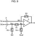
- FIG. 9 A circuit diagram of one example of a conventional comparison circuit is shown in FIG. 9 .
- the conventional comparison circuit uses a comparator (comparator) and determines whether a voltage of a difference between two input voltages is larger or smaller than a predetermined voltage.
- a problem arises in that an offset voltage (input offset voltage) or noise included in the comparator becomes a factor of an error and the accuracy is degraded.
- the above input offset voltage is generated due to variations in the characteristics of each element that configures an input circuit of the comparator by way of example. Further, the above noise is generated due to flicker noise of a single transistor that configures a circuit, or thermal noise of a single transistor or a resistance element.
- the comparison circuit shown in FIG. 9 takes the following configuration.
- the comparison circuit has a comparator 5, a switch S3 connected between an inversion input terminal N3 of the comparator 5 and an output terminal, a capacitor 3 connected between the inversion input terminal N3 of the comparator 5 and an input terminal N1, a switch S4 connected between a non-inversion input terminal N4 of the comparator 5 and a comparison voltage input terminal Nref, a switch S1 connected between the non-inversion input terminal N4 of the comparator 5 and a connection point N41, a capacitor 4 connected between an input terminal N2 and the connection point N41, and a switch S2 connected between the connection point N41 and a comparison voltage input terminal N0.
- a voltage of the comparison voltage input terminal N0 is taken to be V0
- a voltage of the comparison voltage input terminal Nref is taken to be Vref
- a voltage of the input terminal N1 is taken to be V1
- a voltage of the input terminal N2 is taken to be V2
- a voltage of the inversion input terminal N3 of the comparator 5 is taken to be V3
- a voltage of the non-inversion input terminal N4 of the comparator 5 is taken to be V4
- a voltage of the output terminal of the comparator 5 is taken to be Vo.
- the input offset voltage of the comparator 5 is taken to be Voa.
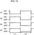
- the comparison circuit of FIG. 9 is operated with the switches S1 to S4 being controlled as shown in FIG. 10 .
- One cycle for the operation consists of a sample phase ⁇ 1 and a comparison phase ⁇ 2.
- the switch S1 is turned off and the switches S2 to S4 are turned on.
- the comparison phase ⁇ 2 the switch S1 is turned on and the switches S2 to S4 are turned off.
- ⁇ 1 or ⁇ 2 attached to the ends of the voltages of each connection point and each terminal is taken to indicate the voltages in the sample phase ⁇ 1 or the comparison phase ⁇ 2 respectively.
- V4 ⁇ 1 Vref since the switch S4 is on.
- the voltage V3 expressed in the equation (45) and the voltage V4 expressed in the equation (46) are compared by the comparator 5, and a high level or a low level is output from the output terminal.
- the comparator 5 compares the input voltage component ⁇ (V2 ⁇ 2-V1 ⁇ 2)-(V2 ⁇ 1-V1 ⁇ 1) ⁇ and the reference voltage component (Vref-V0).
- Vref-V0 the reference voltage component
- Patent Document 1 Japanese Patent Application Laid-Open No. 2008-236737
- US2008/266231 discloses a digital-to-analog conversion circuit includes a gradation voltage generation circuit, a most-significant-bits decoder circuit, a least-significant-bits decoder circuit and a calculation circuit.
- the gradation voltage generation circuit generates multiple main voltages corresponding to most significant bits of the inputted data, and multiple sub voltages corresponding to least significant bits of the inputted data.
- the most-significant-bits decoder circuit selects one of the main voltages in accordance with the most significant bits, and the least-significant-bits decoder circuit selects one of the sub voltages in accordance with the least significant bits.
- the calculator circuit performs calculation processing by use of a first main voltage selected by the most-significant-bits decoder circuit, a first sub voltage selected by the least-significant-bits decoder circuit, and a reference voltage.
- the amount of fluctuation in the voltage at the input of the comparator differs on the inversion input terminal N3 side and the non-inversion input terminal N4 side, and an error has been generated in the comparison result.
- the leak current of the transistor that configures each switch increases as the temperature rises, the higher the temperature becomes, the more the error becomes remarkable.
- the transistor is a MOS transistor, since a leak current between channels depends on the difference in voltage between the drain and source thereof, the flowing direction or magnitude of the leak current of each switch differs due to the voltage on the side not connected to the capacitor in the turned-off switch, and an error has been generated in a comparison result.
- the conventional comparison circuit was accompanied by a problem that since the connections of the switches to the respective capacitors were asymmetrical even as for the influence of noise components (e.g., channel charge injection and clock feed-through) generated when the transistor element that configures each switch was transitioned from on to off, the amount of fluctuation in the voltage at the input of the comparator due to the noise component of each switch differs on the inversion input terminal N3 side and the non-inversion input terminal N4 side, thus resulting in the factor of causing the error.
- noise components e.g., channel charge injection and clock feed-through
- the present invention has been made in view of such points, and aims to provide a comparison circuit capable of removing the influence of an input offset voltage of a comparator with a simple circuit configuration, suppress the influence of an error due to an off-leak current or a noise component of a switch and obtain a highly accurate comparison/determination result.
- switches, capacitors and a comparator are effectively utilized to thereby make it possible to remove with a simple circuit configuration, errors generated due to an offset component generated in the comparator, an off-leak current component of the switch and an noise component of the switch, and perform a highly accurate comparison over a wide temperature region.
- a comparison circuit of the present invention can widely be used as a high accuracy comparison circuit in a semiconductor circuit.
- the comparison circuit of the present invention will hereinafter be described with reference to the drawings.
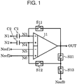
- FIG. 1 is a circuit diagram of a comparison circuit of a first embodiment.
- the comparison circuit of the first embodiment includes a comparator 11, capacitors C1 and C2, and switches S11, S12, S13 and S21.
- the comparator 11 has four input terminals and one output terminal. Specifically, it has a first input terminal N3 of a first differential input pair, a second input terminal N4 of the first differential input pair, a first input terminal N5 of a second differential input pair, a second input terminal N6 of the second differential input pair and an output terminal OUT.
- the capacitor C1 has two terminals, one terminal of which is connected to the first input terminal N3 of the first differential input pair of the comparator 11 and the other terminal thereof is connected to an input terminal N1.
- the capacitor C2 has two terminals, one terminal of which is connected to the second input terminal N4 of the first differential input pair of the comparator 11 and the other terminal thereof is connected to an input terminal N2.
- the switch S11 has two terminals, one terminal of which is connected to the first input terminal N3 of the first differential input pair of the comparator 11 and the other terminal thereof is connected to the output terminal OUT of the comparator 11.
- the switch S12 has two terminals, one terminal of which is connected to the second input terminal N4 of the first differential input pair of the comparator 11.
- the switch S13 has two terminals, one terminal of which is connected to a reference voltage input terminal NrefO.
- the switch S21 has two terminals, one terminal of which is connected to the output terminal OUT of the comparator 11. The other terminals of the switches S12, S13 and S21 are respectively connected in common.
- Each of the switches S11, S12, S13 and S21 is controlled in on/off by a switch control signal (not shown in the circuit diagram).
- a first reference voltage input terminal Nref1 is connected to the first input terminal N5 of the second differential input pair of the comparator 11.
- a second reference voltage input terminal Nref2 is connected to the second input terminal N6 of the second differential input pair of the comparator 11.
- the comparator 11 has the function of outputting the sum of a value obtained by amplifying the difference between a pair of input voltages and a value obtained by amplifying the difference between another pair of input voltages.
- a diagram that conceptually shows this amplifying function is illustrated in FIG. 3 .
- FIG. 3 is a conceptual diagram illustrating the function of the comparator 11.
- the comparator 11 of FIG. 3 has differential amplifiers 111 and 112 and an adder 113 and is connected and configured as follows.
- the first input terminal N3 of the first differential input pair of the comparator 11 is connected to an inversion input terminal of the differential amplifier 111, and the second input terminal N4 of the first differential input pair is connected to a non-inversion input terminal of the differential amplifier 111.
- the first input terminal N5 of the second differential input pair is connected to an inversion input terminal of the differential amplifier 112, and the second input terminal N6 of the second differential input pair is connected to a non-inversion input terminal of the differential amplifier 112.
- the output of the differential amplifier 111 and the output of the differential amplifier 112 are respectively connected to the inputs of the adder 113.
- the output of the adder 113 is connected to the output terminal OUT of the comparator 11.
- the comparator 11 is connected as above and operated as follows.
- the differential amplifier 111 amplifies the difference between the voltages of the two input terminals N3 and N4 and inputs the same to the adder 113.
- the differential amplifier 112 amplifies the difference between the voltages of the two input terminals N5 and N6 and inputs the same to the adder 113.
- the adder 113 outputs the sum of the outputs of the differential amplifier 111 and the differential amplifier 112.
- Vo A 1 / 1 + A 1 ⁇ V 4 + A 2 / 1 + A 1 ⁇ V 6 ⁇ V 5
- Vo V 4 + A 2 / A 1 ⁇ V 6 ⁇ V 5
- the output terminal OUT of the comparator 11 and the first input terminal N3 of the first differential input pair i.e., the inversion input terminal of the differential comparator 111 are electrically connected to each other to form a feedback loop, which performs an operation like a kind of voltage follower that the output voltage Vo not only follows the input voltage V4 but also outputs even a sum with a voltage obtained by amplifying the difference between the voltages of input V6 and V5 with the ratio between the amplification factors A2 and A1.
- the comparator 11 since no feedback loop is formed in the comparator 11 in a state in which the switch S11 is off, the comparator 11 is operated as a comparator itself.
- Vo A 1 ⁇ V 4 ⁇ V 3 + A 2 / A 1 ⁇ V 6 ⁇ V 5 Therefore, in other words, the comparator 11 performs, in the off state of the switch S11, a comparison operation of amplifying, with the sufficiently large amplification factor A1, a voltage of the sum of a voltage of a difference between V4 and V3 and a voltage obtained by amplifying the difference between V6 and V5 with the ratio between the amplification factors A2 and A1, and outputting a high level signal (positive power supply voltage level in general) or a low level signal (negative power supply voltage level or GND level in general) from the output terminal OUT.
- FIG. 2 is a diagram illustrating the operation of each switch.
- One cycle for the comparison operation consists of two phases of a sample phase ⁇ 1 and a comparison phase ⁇ 2.
- the switches S11, S12, S13 and S21 are respectively controlled by switch control signals shown in FIG. 2 .
- the switches S11, S12 and S13 are respectively turned on in the sample phase ⁇ 1 and turned off in the comparison phase ⁇ 2. Further, the switch S21 is turned off in the sample phase ⁇ 1 and turned on in the comparison phase ⁇ 2.
- the sample phase ⁇ 1 is a phase for storing in the capacitors C1 and C2, a voltage V1 of the input terminal N1, a voltage V2 of the input terminal N2, a voltage Vref1 of the first reference voltage input terminal Nref1, a voltage Vref2 of the second reference voltage input terminal Nref2, and an offset voltage of the comparator 11.
- the comparison phase ⁇ 2 is a phase for comparing the difference in voltage between the input terminal N1 and the input terminal N2 and the voltage difference between the first reference voltage Vref1 and the second reference voltage Vref2 while canceling each offset component of the comparator 11 in the sample phase ⁇ 1.
- the switches S11, S12 and S13 are on and the switch S21 is turned off.
- the respective input terminals of the comparator 11 are supplied with the following voltages.
- a voltage Vo of the output terminal OUT is applied to the first input terminal N3 of the first differential input pair of the comparator 11.
- a reference voltage Vref0 is applied to the second input terminal N4 of the first differential input pair.
- the first reference voltage Vref1 is applied to the first input terminal N5 of the second differential input pair.
- the second reference voltage Vref2 is applied to the second input terminal N6 of the second differential input pair.
- V 3 ⁇ ⁇ 1 Vref 0 ⁇ ⁇ 1 + Voa 1 ⁇ ⁇ 1 + A 2 / A 1 ⁇ Vref 2 ⁇ 1 + Voa 2 ⁇ 1 ⁇ Vref 1 ⁇ 1
- the input offset voltages Voa1 and Voa2 of the comparator 11 are not constant values because they strictly indicate a temporal change and a change in temperature (temperature drift). If, however, the times taken for the sample phase ⁇ 1 and the comparison phase ⁇ 2 are times sufficiently short relative to the temporal and temperature changes in the input offset voltages, the values of the input offset voltages can be assumed to be approximately equal values in the sample phase ⁇ 1 and the comparison phase ⁇ 2. Accordingly, in the equation (18), Voa1 ⁇ 2-Voa1 ⁇ 1 and Voa2 ⁇ 2-Voa2 ⁇ 1 become values of almost zero, and the offset components of the comparator 11 are removed upon the comparison operation by the comparator 11 in the comparison phase ⁇ 2.
- a result of comparison between the voltage components ⁇ Vin supplied from the input terminal N1 and the input terminal N2 and the voltage components ⁇ Vref supplied from the first reference voltage input terminal Nref1 and the second reference voltage input terminal Nref2 is amplified with a sufficiently large amplification factor A1 and eventually outputted as a high level signal or a low level signal from the output terminal OUT of the comparator 11.
- Vref0 When attention is paid to the equation (17) here, the term of Vref0 is not included in this equation. This is because the term of Vref0 ⁇ 1 is included in both of the voltage ⁇ VC1 ⁇ 1 charged in the capacitor C1 and ⁇ VC2 ⁇ 1 charged in the capacitor C2, and the term of Vref0 is cancelled in the process of deriving Vo ⁇ 2. This indicates that in the comparison circuit of the present embodiment, the comparison result does not depend on the voltage of Vref0 even if the voltage applied to the reference voltage input terminal Nref0 takes any value. In an actual circuit, there is a restriction of an in-phase input voltage range on the range of voltages inputtable to the comparator 11.
- a comparison circuit-magnetic sensor device of the present embodiment has an advantage in that the highly accurate comparison is made possible by selecting the voltage of the reference voltage input terminal Nref0 to fall within the in-phase input voltage range of the comparator 11. If another expression is taken, it can be said that it has an advantage in that the in-phase input voltage range required for the comparator 11 can remarkably be relaxed.
- the switch S13 is turned off and the switch S21 is turned off to perform an operation so as to make the voltage of the other terminal of the switch S12 equal to the voltage Vo of the output terminal OUT of the comparator 11. Accordingly, the voltages of the other terminals of the switches S11 and S12 held in an off state become equal to the voltage Vo of the output terminal OUT of the comparator 11.
- the switch S13 remains on in the comparison phase ⁇ 2 similarly to the sample phase ⁇ 1, and the switch S21 remains off in the comparison phase ⁇ 2 similarly to the sample phase ⁇ 1, in other words, the switches S13 and S21 do not exist and the other terminal of the switch S12 is directly connected to the reference voltage input terminal Nref0.
- the other voltage of the switch S11 becomes equal to the voltage Vo of the output terminal OUT of the comparator 11 and becomes a voltage of a high level signal (positive power supply voltage level in general) or a low level signal (negative power supply voltage level or GND level in general) according to the result of comparison.
- the other voltage of the switch S12 becomes equal to the voltage of the reference voltage input terminal NrefO.
- the voltage of the reference voltage input terminal Nref0 is preferably selected to fall within the in-phase input voltage range of the comparator 11.
- the voltage of the reference voltage input terminal Nref0 is set to a voltage between the positive power supply voltage level and the negative power supply level (or GND level), for example, an intermediate voltage. Accordingly, in the comparison phase ⁇ 2, the voltage of the other terminal of the switch S11 and the voltage of the other terminal of the switch S21 become voltages very large in difference.
- the voltages of one terminals of the switches S11 and S12 are the voltages expressed by the equations (13) and (15) respectively.
- both become voltages based on the voltage of the reference voltage input terminal Nref0 in the sample phase ⁇ 1 and become voltages approximately close to each other particularly near a boundary condition under which a comparison/determination result of the comparator 11 is switched (at least there no occurs a voltage difference of such an extent that one of the voltages becomes a positive or negative power supply voltage and the other thereof becomes an intermediate voltage between the positive and negative power supply voltages).
- the voltage of one terminal corresponds to the voltage based on the Vref0 ⁇ 1 expressed in the equation (13), and the voltage of the other terminal is equal to the voltage Vo of the output terminal OUT of the comparator 11 and corresponds to the voltage of the high level signal (positive power supply voltage level in general) or the low level signal (negative power supply voltage level or GND level in general), a current leak current larger than the leak current of the switch S12 flows.
- the leak currents that flow in the capacitor C1 and the capacitor C2 differ from each other, and the amount of fluctuation in the voltage of the first input terminal N3 of the first differential input pair and the amount of fluctuation in the voltage of the second input terminal N4 of the first differential input pair differ from each other, thus resulting in a factor that an error occurs in the result of comparison.
- the leak current tends to increase with raising of the temperature, the error of the comparison circuit increases as the temperature becomes higher.
- the switch S13 in the comparison phase ⁇ 2, the switch S13 is turned off and the switch S21 is turned on to control the voltage of the other terminal of the switch S12 to be equal to the voltage Vo of the output terminal OUT of the comparator 11. Therefore, the difference between the difference in voltage between both terminals of the switch S11 and the difference in voltage between both terminals of the switch S12 is improved so as to be small, so that the difference between the leak currents becomes small.
- the difference between the leak currents that flow in the capacitor C1 and the capacitor C2 is improved so as to be small, and as a result, the error that occurs in the result of comparison can be reduced. Accordingly, the influence of the error caused by the leak current of each switch can be suppressed by the switches S13 and S21, and a highly accurate comparison/determination result can hence be obtained.
- the nonideal components of the switch include, in addition to the above leak current, a noise component generated when a transistor element that configures each switch is transitioned from on to off, e.g., channel charge injection and clock feed-through.
- the present embodiment is operated in such a manner that since the switches S11 and S12 are connected to a connection point of one terminal of the capacitor C1 and the first input terminal N3 of the first differential input pair of the comparator 11, and a connection point of one terminal of the capacitor C2 and the second input terminal N4 of the first differential input pair of the comparator 11 such that they become symmetrical with respect to each other respectively, electrical charges generated due to the noise components of the switches are approximately equally injected to the respective connection points, and the amounts of fluctuations in the voltage of the first input terminal N3 of the first differential input pair and the voltage of the second input terminal N4 of the first differential input pair become approximately equal to each other though both voltages fluctuate. Accordingly, it is possible to suppress the influence of errors due to the noise components generated when the switch is transitioned from
- comparator 11 being an element that configures the magnetic sensor device of FIG. 1
- the function of the comparator 11 shown by the conceptual diagram of FIG. 3 can more specifically be realized by such a circuit configuration as shown in FIG. 4 by way of example.
- FIG. 4 is one example of the circuit configuration of the comparator 11.
- the comparator 11 has a constant current circuit I1, NMOS transistors M13, M14A, M14B, M15A, M16B, M15B and M16B, and PMOS transistors M11 and M12 and is connected and configured as follows.
- One of the constant current I1 is connected to a power supply voltage terminal VDD, and the other thereof is connected to a drain and gate of the NMOS transistor M13. This connection point is taken to be Nb.
- Nb is connected to a gate of the NMOS transistor M14A and a gate of the NMOS transistor M14B.
- Sources of the NMOS transistors M13, M14A and M14B are connected to a ground terminal VSS.
- Sources of the NMOS transistors M15A and M16A are connected to a drain of M14A.
- Sources of the NMOS transistors M15B and M16B are connected to a drain of M14B.
- Drains of the NMOS transistors M15A and M15B are connected to a drain of the PMOS transistor M11. This connection point is taken to be Na.
- Drains of the NMOS transistors M16A and M16B are connected to a drain of the PMOS transistor M12. This connection point is connected to an output terminal OUT of the comparator 11.
- Gates of the PMOS transistors M11 and M12 are connected to the connection point Na, and sources thereof are connected to the power supply voltage terminal VDD.
- Gates of the NMOS transistors M15A and M16A are respectively connected to the second input terminal N4 and first input terminal N3 of the first differential input pair.
- Gates of the NMOS transistors M15B and M16B are respectively connected to the second input terminal N6 and first input terminal N5 of the second differential input pair.
- the comparator 11 is connected as described above and operated as follows.
- the constant current circuit I1 generates a constant current and supplies it to the NMOS transistor M13.
- the NMOS transistors M13, M14A and M14B configure a current mirror circuit. A current based on a current that flows between the drain and source of M13 flows between the drains and sources of the NMOS transistors M14A and M14B.
- the five transistors comprised of the NMOS transistors M14A, M15A and M16A and the PMOS transistors M11 and M12 configure a differential amplifier and are operated to amplify the difference in voltage between the gates of the NMOS transistors M15A and M16A that configure the first differential input pair, i.e., the difference in voltage between the second input terminal N4 of the first differential input pair and the first input terminal N3 of the first differential input pair and output it to the output terminal OUT.
- This amplification factor is taken to be A1.
- the operations of the current mirror circuit configuration and the differential amplifier configuration have been described in detail in a document of a CMOS analog circuit or the like. A detail description thereof will be omitted here.
- the five transistors comprised of the NMOS transistors M14B, M15B and M16B and the PMOS transistors M11 and M12 also configure a differential amplifier and are operated to amplify the difference in voltage between the gates of the NMOS transistors M15B and M16B that configure the second differential input pair, i.e., the difference in voltage between the second input terminal N6 of the second differential input pair and the first input terminal N5 of the second differential input pair and output it to the output terminal OUT.
- This amplification factor is taken to be A2.
- the drain of the NMOS transistor M15A that configures the first differential input pair, and the drain of the NMOS transistor M15B that configures the second differential input pair are connected to the drain of the PMOS transistor M11 at the connection point Na
- the drain of the NMOS transistor M16A that configures the first differential input pair and the drain of the NMOS transistor M16B that configure the second differential input pair are connected to the drain of the PMOS transistor M12 at the output terminal OUT, whereby the voltages amplified by the respective differential input pairs of the first differential input pair and the second differential input pair are operated so as to be added at the connection point Na and the output terminal OUT.
- the comparator 11 is not necessarily limited to this configuration if a configuration is adopted which performs the operations described in the present description. While the timings at which the on or off of the switches is switched upon transition from the sample phase ⁇ 1 to the comparison phase ⁇ 2 or the reverse transition have been described to be provided simultaneously in FIG. 2 , for example, each timing may be controlled to be shifted such that the switch S12 is turned off after turning off of the switch S11 and further, thereafter S13 is turned off and S21 is turned on.
- the timing at which the switch S12 is turned off is more preferably delayed than the timing at which the switch S11 is turned off.
- the present description includes one example of the input voltages applied to the input terminal N1 and the input terminal N2, and one example of the voltages applied to the first reference voltage input terminal Nref1 and the second reference voltage input terminal Nref2, but is not necessarily limited thereto.
- Vcm is an in-phase voltage component of a signal voltage of the sensor element
- Vsig is a signal voltage component of the sensor element
- Voff is an offset voltage component (error factor) of the sensor element.
- the offset voltage components of the sensor element indicate values approximately equal to each other in the sample phase ⁇ 1 and the comparison phase ⁇ 2, they are cancelled. Accordingly, only the signal voltage components of the sensor element are input to the comparator 11 as the input voltage components. Even such a case of input voltage components will not depart from the viewpoint corresponding to the gist of the present invention, of removing the influence of the input offset voltages of the comparator and suppressing the influence of the error due to the off-leak current or noise component of the switch, and obtaining the highly accurate comparison/determination result.
- FIG. 5 is a circuit diagram of a comparison circuit of a second embodiment.
- a difference from the first embodiment shown in FIG. 1 resides in that the switches S13 and S21 are omitted and switches S14 and S22 are added.
- the added elements are configured and connected as follows. The following connections differ from the first embodiment due to the omitted elements.
- the other terminal of a switch S12 is connected to a reference voltage input terminal NrefO.
- the switch S14 has two terminals, one terminal of which is connected to an output terminal OUT of a comparator 11 and the other terminal thereof is connected to the other terminal of a switch S11.
- the switch S22 has two terminals, one terminal of which is connected to the other terminal of the switch S11 and the other terminal thereof is connected to the other terminal of the switch S12. This other connection and configuration are the same as the first embodiment.
- the switches S14 and S22 are controlled in on/off by switch control signals (not shown in the circuit diagram) in a manner similar to the switches S11 and S12.
- FIG. 6 is a diagram illustrating the operation of each switch in the comparison circuit of the second embodiment.
- the switches S11, S12 and S14 are controlled to be turned on in a sample phase ⁇ 1 and turned off in a comparison phase ⁇ 2.
- the switch S22 is controlled to be turned off in the sample phase ⁇ 1 and turned on in the comparison phase ⁇ 2.
- the switches S11, S12 and S14 are on and the switch S22 is turned off. Accordingly, the following voltages are supplied to each input terminal of the comparator 11.
- a voltage Vo of the output terminal OUT is applied to a first input terminal N3 of a first differential input pair of the comparator 11.
- a voltage of the reference voltage input terminal NrefO is applied to a second input terminal N4 of the first differential input pair.
- a voltage of a first reference voltage input terminal Nref1 is applied to a first input terminal N5 of a second differential input pair.
- a voltage of a second reference voltage input terminal Nref2 is applied to a second input terminal N6 of the second differential input pair. That is, since the above is similar to the comparison circuit of the first embodiment, the operation also becomes similar to the comparison circuit of the first embodiment.
- the switches S11, S12 and S14 are off and the switch S22 is turned on. Since the switches S11 and S12 are off, a voltage V3 is determined by a voltage V1 and ⁇ VC1 ⁇ 1, and a voltage V4 is determined by a voltage V2 and ⁇ VC2 ⁇ 1. That is, since the above is similar to the comparison circuit of the first embodiment, the operation also becomes similar to the comparison circuit of the first embodiment.
- the switch S14 Since in the comparison phase ⁇ 2, the switch S14 is turned off and the switch S22 is on, the voltages of the other terminals of the switches S11 and S12 become equal to the voltage of the reference voltage input terminal NrefO. In the case of the comparison circuit of the first embodiment, the voltages of the other terminals of the switches S11 and S12 are equal to the voltage Vo of the output terminal OUT of the comparator 11. This point therefore differs from the first embodiment. In the present embodiment, the switch S14 is turned off and the switch S22 is turned on in the comparison phase ⁇ 2. Thus, since the voltage of one terminal of the switch S12 becomes a voltage based on the Vref0 ⁇ 1 expressed in the equation (15), and the voltage of the other terminal thereof becomes the voltage of Vref0 ⁇ 1.
- the leak current becomes a relatively small leak current although it flows. Since, in regard to the switch S11, the voltage of one terminal thereof becomes a voltage based on Vref0 ⁇ 1 expressed in the equation (13), and the voltage of the other terminal thereof becomes the voltage of Vref0 ⁇ 1, the leak current becomes a relatively small leak current although it flows as with the switch S12. Thus, the difference between the difference in voltage between both terminals of the switch S11 and the difference in voltage between both terminals of the switch S12 is improved so as to be small. As with the case of the comparison circuit of the first embodiment, an error that occurs in a comparison/determination result can be reduced as a result. Accordingly, the switches S14 and S22 make it possible to suppress the influence of an error generated by the leak current of each switch and obtain a highly accurate comparison/determination result.
- the nonideal components of the switch include, in addition to the above leak current, a noise component generated when a transistor element that configures a switch is transitioned from on to off, e.g., channel charge injection and clock feed-through.
- the present embodiment is operated in such a manner that since the switches S11 and S12 are connected to a connection point of one terminal of the capacitor C1 and the first input terminal N3 of the first differential input pair of the comparator 11, and a connection point of one terminal of the capacitor C2 and the second input terminal N4 of the first differential input pair of the comparator 11 such that they become symmetrical with respect to each other respectively, electrical charges generated due to the noise components of the switches are approximately equally injected to the respective connection points, and the amounts of fluctuations in the voltage of the first input terminal N3 of the first differential input pair and the voltage of the second input terminal N4 of the first differential input pair become approximately equal to each other though both voltages fluctuate.
- FIG. 7 is a circuit diagram of a comparison circuit of a third embodiment. Differences from the first embodiment shown in FIG. 1 reside in that the comparator 11 is replaced with a comparator 12, and the first reference voltage input terminal Nref1 and the second reference voltage input terminal Nref2 connected to the input of the comparator 11 are omitted.
- the replaced element is configured and connected as follows.
- the comparator 12 has two input terminals and an output terminal. Specifically, the comparator 12 has a first input terminal N3 of a differential input pair, a second input terminal N4 of the differential input pair, and an output terminal OUT.
- the first input terminal N3 of the differential input pair of the comparator 12 is connected to one terminal of a capacitor C1
- the second input terminal N4 of the differential input pair is connected to one terminal of a capacitor C2
- the output terminal OUT is connected to the other terminal of a switch S11.
- This other connection and configuration are the same as the first embodiment.
- the switches S11, S12, S13 and S21 are controlled in on/off by switch control signals (not shown in the circuit diagram) as with the comparison circuit of the first embodiment.
- the comparator 12 has the function of outputting a value obtained by amplifying a difference between input voltages.
- the output terminal OUT of the comparator 12 and the first input terminal N3 of the differential input pair are electrically connected to form a feedback loop, which performs a voltage follower operation by following the output voltage Vo to the input voltage V4.
- the comparator 11 since no feedback loop is formed in the comparator 12 in a state in which the switch S11 is off, the comparator 11 is operated as a comparator (comparator) itself.
- each switch is also controlled in a manner similar to the first embodiment and is made active in accordance with the diagram showing the operation of each switch in FIG. 2 .
- the outline of operation of the comparison circuit of FIG. 7 in each phase will be described.
- the sample phase ⁇ 1 is a phase for storing in the capacitors C1 and C2, respective terminal voltage of the input terminal N1 and the input terminal N2 and an offset voltage of the comparator 12.
- the comparison phase ⁇ 2 is a phase for performing a comparison of the difference in voltage between the input terminal N1 and the input terminal N2 while canceling an offset component of the comparator 12 in the sample phase ⁇ 1. Details thereof will be described below.
- the input offset voltage Voa3 of the comparator 12 can be assumed to be approximately equal values in the sample phase ⁇ 1 and the comparison phase ⁇ 2 if the times taken for the sample phase ⁇ 1 and the comparison phase ⁇ 2 are times sufficiently short relative to temporal and temperature changes in the input offset voltage. Accordingly, in the equation (41), Voa3 ⁇ 2-Voa3 ⁇ 1 become a value of almost zero, and the offset component of the comparator 12 is removed upon the comparison operation by the comparator 12 in the comparison phase ⁇ 2.
- A3 sufficiently large amplification factor
- Vref0 is not included in the equation (42). As with the first embodiment, this is advantageous in that a highly accurate comparison is made possible by selecting the voltage of the reference voltage input terminal Nref0 to fall within the in-phase input voltage range of the comparator 12 even if the voltages of the input terminal N1 and the input terminal N2 fall outside the in-phase input voltage range of the comparator 12. If another expression is taken, it can be said that it is advantageous in that the in-phase input voltage range required for the comparator 12 can remarkably be relaxed.
- the switch S13 and S21 the switch S13 is turned off and the switch S21 is turned on in the comparison phase ⁇ 2 to perform an operation in such a manner that the voltages of the other terminals of the switch S11 and the switch S12 become equal to the voltage Vo of the output terminal OUT of the comparator 11. Accordingly, as with the first embodiment, the switches S13 and S21 make it possible to suppress the influence of an error generated by a leak current of each switch and obtain a highly accurate comparison/determination result.
- the influence of an error due to a noise component generated when the switch is transitioned from an on state to an off state can be suppressed, and a highly accurate comparison/determination result can be obtained.
- comparison circuit of the third embodiment has been described as above. It has been shown that it is possible to remove the influence of the input offset voltage of the comparator with a simple circuit configuration, suppress the influence of an error due to an off-leak current or a noise component of each switch and obtain a highly accurate comparison/determination result.
- FIG. 8 is a circuit diagram of a comparison circuit of a fourth embodiment. Differences from the third embodiment shown in FIG. 7 reside in that the switches S13 and S21 are omitted and switches S14 and S22 are added. The added elements are configured and connected as follows. The following connections differ from the third embodiment due to the omitted elements.
- the other terminal of a switch S12 is connected to a reference voltage input terminal Nref0.
- the switch S14 has two terminals, one terminal of which is connected to an output terminal OUT of a comparator 12 and the other terminal thereof is connected to the other terminal of a switch S11.
- the switch S22 has two terminals, one terminal of which is connected to the other terminal of the switch S11, and the other terminal thereof is connected to the other terminal of the switch S12, This other connection and configuration are the same as the third embodiment.
- differences between the present embodiment and the second embodiment shown in FIG. 5 reside in that as with the differences between the third embodiment shown in FIG. 7 and the first embodiment shown in FIG. 1 , the comparator 11 is replaced with a comparator 12, and the first reference voltage input terminal Nref1 and the second reference voltage input terminal Nref2 connected to the input of the comparator 11 are omitted.
- the switches S14 and S22 are controlled in on/off by switch control signals (not shown in the circuit diagram) in a manner similar to the switches S11 and S12.
- the operation of each switch is controlled as with the second embodiment and is made active in accordance with the diagram showing the operation of each switch in FIG. 6 .
- each input terminal of the comparator 12 is supplied with the following voltages.
- a voltage Vo of the output terminal OUT is applied to a first input terminal N3 of a differential input pair of the comparator 12.
- a voltage of the reference voltage input terminal NrefO is applied to a second input terminal N4 of the differential input pair. That is, since the above is similar to the comparison circuit of the third embodiment, the operation also becomes similar to the comparison circuit of the third embodiment.
- a comparison phase ⁇ 2 the switches S11, S12 and S14 are on and the switch S22 is turned on. Since the switches S11 and S12 are off, a voltage V3 is determined by a voltage V1 and ⁇ VC1 ⁇ 1, and a voltage V4 is determined by a voltage V2 and ⁇ VC2 ⁇ 1. That is, there is provided the comparison circuit capable of obtaining a highly accurate comparison/determination result, which becomes similar even in operation to the comparison circuit of the third embodiment since the above is similar to the comparison circuit of the third embodiment and which has an advantage that it is possible to remove an offset component of the comparator 12 and remarkably relax an in-phase input voltage range required for the comparator 12.
- the comparison circuit capable of suppressing the influence of an error due to a leak current of each of the switches S11 and S12 and obtaining a highly accurate comparison/determination result since the above is similar to the comparison circuit of the second embodiment.
- comparison circuit of the fourth embodiment has been described as above. It has been shown that it is possible to remove the influence of an input offset voltage of the comparator with a simple circuit configuration, suppress the influence of an error due to an off-leak current or a noise component of each switch and obtain a highly accurate comparison/determination result in a manner similar to the third embodiment.
Landscapes
- Physics & Mathematics (AREA)
- Nonlinear Science (AREA)
- Engineering & Computer Science (AREA)
- Power Engineering (AREA)
- Manipulation Of Pulses (AREA)
Applications Claiming Priority (2)
| Application Number | Priority Date | Filing Date | Title |
|---|---|---|---|
| JP2013233408A JP6454065B2 (ja) | 2013-11-11 | 2013-11-11 | 比較回路 |
| PCT/JP2014/076908 WO2015068517A1 (ja) | 2013-11-11 | 2014-10-08 | 比較回路 |
Publications (3)
| Publication Number | Publication Date |
|---|---|
| EP3070845A1 EP3070845A1 (en) | 2016-09-21 |
| EP3070845A4 EP3070845A4 (en) | 2017-11-22 |
| EP3070845B1 true EP3070845B1 (en) | 2019-12-18 |
Family
ID=53041300
Family Applications (1)
| Application Number | Title | Priority Date | Filing Date |
|---|---|---|---|
| EP14860009.1A Active EP3070845B1 (en) | 2013-11-11 | 2014-10-08 | Comparison circuit |
Country Status (7)
| Country | Link |
|---|---|
| US (1) | US9768758B2 (zh) |
| EP (1) | EP3070845B1 (zh) |
| JP (1) | JP6454065B2 (zh) |
| KR (1) | KR102153872B1 (zh) |
| CN (1) | CN105960757B (zh) |
| TW (1) | TWI637600B (zh) |
| WO (1) | WO2015068517A1 (zh) |
Families Citing this family (2)
| Publication number | Priority date | Publication date | Assignee | Title |
|---|---|---|---|---|
| JP6998741B2 (ja) * | 2017-11-20 | 2022-01-18 | エイブリック株式会社 | センサ装置 |
| JP2022146999A (ja) | 2021-03-23 | 2022-10-06 | エイブリック株式会社 | 半導体装置 |
Family Cites Families (14)
| Publication number | Priority date | Publication date | Assignee | Title |
|---|---|---|---|---|
| JPH043520A (ja) * | 1990-04-20 | 1992-01-08 | Nec Corp | 比較回路 |
| JP3454689B2 (ja) * | 1997-09-30 | 2003-10-06 | 三洋電機株式会社 | 電圧比較器、演算増幅器、アナログ−デジタル変換器およびアナログ−デジタル変換回路 |
| JP4901720B2 (ja) * | 2005-02-08 | 2012-03-21 | ローム株式会社 | 磁気センサ回路、及び、その磁気センサ回路を有する携帯端末 |
| JP5334366B2 (ja) * | 2006-12-15 | 2013-11-06 | 三菱電機株式会社 | 半導体集積回路 |
| US7570044B2 (en) * | 2007-02-19 | 2009-08-04 | Kabushiki Kaisha Toshiba | Signal detecting circuit |
| US8242944B2 (en) * | 2007-04-26 | 2012-08-14 | Renesas Electronics Corporation | Digital-to-analog converter circuit including adder drive circuit and display |
| CN101330284B (zh) * | 2007-06-19 | 2011-05-04 | 智原科技股份有限公司 | 时间常数校正装置及其相关方法 |
| CN101431233B (zh) * | 2008-08-21 | 2012-05-23 | 艾默生网络能源有限公司 | 恒功率输出电源的检测保护电路 |
| JP4956573B2 (ja) * | 2009-03-19 | 2012-06-20 | 株式会社東芝 | 増幅回路及び磁気センサ |
| TWI480526B (zh) * | 2009-12-24 | 2015-04-11 | Seiko Epson Corp | 紅外線檢測電路、感測器裝置及電子機器 |
| TWI443969B (zh) * | 2010-11-17 | 2014-07-01 | Ind Tech Res Inst | 以動態比較器為基礎的比較系統 |
| CN102914734B (zh) * | 2011-08-04 | 2015-04-08 | 台达电子企业管理(上海)有限公司 | 气体放电灯寿终检测电路及其所适用的安定器 |
| JP5926081B2 (ja) * | 2012-03-22 | 2016-05-25 | エスアイアイ・セミコンダクタ株式会社 | センサ装置 |
| JP6180752B2 (ja) * | 2012-04-27 | 2017-08-16 | エスアイアイ・セミコンダクタ株式会社 | センサ装置 |
-
2013
- 2013-11-11 JP JP2013233408A patent/JP6454065B2/ja active Active
-
2014
- 2014-10-08 KR KR1020167012230A patent/KR102153872B1/ko active IP Right Grant
- 2014-10-08 WO PCT/JP2014/076908 patent/WO2015068517A1/ja active Application Filing
- 2014-10-08 CN CN201480061760.1A patent/CN105960757B/zh active Active
- 2014-10-08 EP EP14860009.1A patent/EP3070845B1/en active Active
- 2014-10-21 TW TW103136293A patent/TWI637600B/zh active
-
2016
- 2016-04-27 US US15/139,777 patent/US9768758B2/en active Active
Non-Patent Citations (1)
| Title |
|---|
| None * |
Also Published As
| Publication number | Publication date |
|---|---|
| KR102153872B1 (ko) | 2020-09-09 |
| JP6454065B2 (ja) | 2019-01-16 |
| EP3070845A1 (en) | 2016-09-21 |
| JP2015095727A (ja) | 2015-05-18 |
| EP3070845A4 (en) | 2017-11-22 |
| CN105960757B (zh) | 2019-07-09 |
| KR20160085262A (ko) | 2016-07-15 |
| TW201539983A (zh) | 2015-10-16 |
| TWI637600B (zh) | 2018-10-01 |
| US20160241222A1 (en) | 2016-08-18 |
| CN105960757A (zh) | 2016-09-21 |
| US9768758B2 (en) | 2017-09-19 |
| WO2015068517A1 (ja) | 2015-05-14 |
Similar Documents
| Publication | Publication Date | Title |
|---|---|---|
| US9166541B2 (en) | Signal processing circuit, resolver digital converter, and multipath nested mirror amplifier | |
| JP5412639B2 (ja) | 比較器及びアナログデジタル変換器 | |
| US8836376B2 (en) | Comparator and A/D converter | |
| US7864093B2 (en) | Pulse phase difference detecting circuit and A/D converter using the same | |
| US8836375B2 (en) | Continuously self-calibrated latched comparator | |
| KR100940475B1 (ko) | A/d 변환기 | |
| EP2829889B1 (en) | Sensor device | |
| JP2017526247A (ja) | Dcオフセット自動ゼロ化を有するシングルオペアンプを使用した電流感知回路 | |
| KR101562898B1 (ko) | Op 앰프 | |
| US20150115925A1 (en) | A/d converter and semiconductor integrated circuit | |
| US8456343B2 (en) | Switched capacitor type D/A converter | |
| Xu et al. | Offset-corrected 5GHz CMOS dynamic comparator using bulk voltage trimming: Design and analysis | |
| EP3070845B1 (en) | Comparison circuit | |
| US10985721B2 (en) | Switched capacitor amplifier circuit, voltage amplification method, and infrared sensor device | |
| US20100289936A1 (en) | Buffer circuit, image sensor chip comprising the same, and image pickup device | |
| US9837997B2 (en) | Comparison circuit and sensor device | |
| US8232904B2 (en) | Folding analog-to-digital converter | |
| KR101295190B1 (ko) | 스위치드 캐패시터 연산증폭기 | |
| US10630278B2 (en) | Electronic circuit and control method for electronic circuit | |
| JP2013207697A (ja) | サンプル・ホールド回路 |
Legal Events
| Date | Code | Title | Description |
|---|---|---|---|
| PUAI | Public reference made under article 153(3) epc to a published international application that has entered the european phase |
Free format text: ORIGINAL CODE: 0009012 |
|
| 17P | Request for examination filed |
Effective date: 20160613 |
|
| AK | Designated contracting states |
Kind code of ref document: A1 Designated state(s): AL AT BE BG CH CY CZ DE DK EE ES FI FR GB GR HR HU IE IS IT LI LT LU LV MC MK MT NL NO PL PT RO RS SE SI SK SM TR |
|
| AX | Request for extension of the european patent |
Extension state: BA ME |
|
| DAX | Request for extension of the european patent (deleted) | ||
| A4 | Supplementary search report drawn up and despatched |
Effective date: 20171019 |
|
| RIC1 | Information provided on ipc code assigned before grant |
Ipc: H03K 5/08 20060101AFI20171013BHEP |
|
| RAP1 | Party data changed (applicant data changed or rights of an application transferred) |
Owner name: ABLIC INC. |
|
| GRAP | Despatch of communication of intention to grant a patent |
Free format text: ORIGINAL CODE: EPIDOSNIGR1 |
|
| STAA | Information on the status of an ep patent application or granted ep patent |
Free format text: STATUS: GRANT OF PATENT IS INTENDED |
|
| INTG | Intention to grant announced |
Effective date: 20190814 |
|
| GRAS | Grant fee paid |
Free format text: ORIGINAL CODE: EPIDOSNIGR3 |
|
| GRAA | (expected) grant |
Free format text: ORIGINAL CODE: 0009210 |
|
| STAA | Information on the status of an ep patent application or granted ep patent |
Free format text: STATUS: THE PATENT HAS BEEN GRANTED |
|
| AK | Designated contracting states |
Kind code of ref document: B1 Designated state(s): AL AT BE BG CH CY CZ DE DK EE ES FI FR GB GR HR HU IE IS IT LI LT LU LV MC MK MT NL NO PL PT RO RS SE SI SK SM TR |
|
| REG | Reference to a national code |
Ref country code: CH Ref legal event code: EP |
|
| REG | Reference to a national code |
Ref country code: IE Ref legal event code: FG4D |
|
| REG | Reference to a national code |
Ref country code: AT Ref legal event code: REF Ref document number: 1215686 Country of ref document: AT Kind code of ref document: T Effective date: 20200115 |
|
| REG | Reference to a national code |
Ref country code: DE Ref legal event code: R096 Ref document number: 602014058738 Country of ref document: DE |
|
| REG | Reference to a national code |
Ref country code: NL Ref legal event code: MP Effective date: 20191218 |
|
| PG25 | Lapsed in a contracting state [announced via postgrant information from national office to epo] |
Ref country code: LT Free format text: LAPSE BECAUSE OF FAILURE TO SUBMIT A TRANSLATION OF THE DESCRIPTION OR TO PAY THE FEE WITHIN THE PRESCRIBED TIME-LIMIT Effective date: 20191218 Ref country code: GR Free format text: LAPSE BECAUSE OF FAILURE TO SUBMIT A TRANSLATION OF THE DESCRIPTION OR TO PAY THE FEE WITHIN THE PRESCRIBED TIME-LIMIT Effective date: 20200319 Ref country code: NO Free format text: LAPSE BECAUSE OF FAILURE TO SUBMIT A TRANSLATION OF THE DESCRIPTION OR TO PAY THE FEE WITHIN THE PRESCRIBED TIME-LIMIT Effective date: 20200318 Ref country code: LV Free format text: LAPSE BECAUSE OF FAILURE TO SUBMIT A TRANSLATION OF THE DESCRIPTION OR TO PAY THE FEE WITHIN THE PRESCRIBED TIME-LIMIT Effective date: 20191218 Ref country code: SE Free format text: LAPSE BECAUSE OF FAILURE TO SUBMIT A TRANSLATION OF THE DESCRIPTION OR TO PAY THE FEE WITHIN THE PRESCRIBED TIME-LIMIT Effective date: 20191218 Ref country code: BG Free format text: LAPSE BECAUSE OF FAILURE TO SUBMIT A TRANSLATION OF THE DESCRIPTION OR TO PAY THE FEE WITHIN THE PRESCRIBED TIME-LIMIT Effective date: 20200318 Ref country code: FI Free format text: LAPSE BECAUSE OF FAILURE TO SUBMIT A TRANSLATION OF THE DESCRIPTION OR TO PAY THE FEE WITHIN THE PRESCRIBED TIME-LIMIT Effective date: 20191218 |
|
| REG | Reference to a national code |
Ref country code: LT Ref legal event code: MG4D |
|
| PG25 | Lapsed in a contracting state [announced via postgrant information from national office to epo] |
Ref country code: RS Free format text: LAPSE BECAUSE OF FAILURE TO SUBMIT A TRANSLATION OF THE DESCRIPTION OR TO PAY THE FEE WITHIN THE PRESCRIBED TIME-LIMIT Effective date: 20191218 Ref country code: HR Free format text: LAPSE BECAUSE OF FAILURE TO SUBMIT A TRANSLATION OF THE DESCRIPTION OR TO PAY THE FEE WITHIN THE PRESCRIBED TIME-LIMIT Effective date: 20191218 |
|
| PG25 | Lapsed in a contracting state [announced via postgrant information from national office to epo] |
Ref country code: AL Free format text: LAPSE BECAUSE OF FAILURE TO SUBMIT A TRANSLATION OF THE DESCRIPTION OR TO PAY THE FEE WITHIN THE PRESCRIBED TIME-LIMIT Effective date: 20191218 |
|
| PG25 | Lapsed in a contracting state [announced via postgrant information from national office to epo] |
Ref country code: PT Free format text: LAPSE BECAUSE OF FAILURE TO SUBMIT A TRANSLATION OF THE DESCRIPTION OR TO PAY THE FEE WITHIN THE PRESCRIBED TIME-LIMIT Effective date: 20200513 Ref country code: EE Free format text: LAPSE BECAUSE OF FAILURE TO SUBMIT A TRANSLATION OF THE DESCRIPTION OR TO PAY THE FEE WITHIN THE PRESCRIBED TIME-LIMIT Effective date: 20191218 Ref country code: RO Free format text: LAPSE BECAUSE OF FAILURE TO SUBMIT A TRANSLATION OF THE DESCRIPTION OR TO PAY THE FEE WITHIN THE PRESCRIBED TIME-LIMIT Effective date: 20191218 Ref country code: CZ Free format text: LAPSE BECAUSE OF FAILURE TO SUBMIT A TRANSLATION OF THE DESCRIPTION OR TO PAY THE FEE WITHIN THE PRESCRIBED TIME-LIMIT Effective date: 20191218 Ref country code: NL Free format text: LAPSE BECAUSE OF FAILURE TO SUBMIT A TRANSLATION OF THE DESCRIPTION OR TO PAY THE FEE WITHIN THE PRESCRIBED TIME-LIMIT Effective date: 20191218 |
|
| PG25 | Lapsed in a contracting state [announced via postgrant information from national office to epo] |
Ref country code: IS Free format text: LAPSE BECAUSE OF FAILURE TO SUBMIT A TRANSLATION OF THE DESCRIPTION OR TO PAY THE FEE WITHIN THE PRESCRIBED TIME-LIMIT Effective date: 20200418 Ref country code: SK Free format text: LAPSE BECAUSE OF FAILURE TO SUBMIT A TRANSLATION OF THE DESCRIPTION OR TO PAY THE FEE WITHIN THE PRESCRIBED TIME-LIMIT Effective date: 20191218 Ref country code: SM Free format text: LAPSE BECAUSE OF FAILURE TO SUBMIT A TRANSLATION OF THE DESCRIPTION OR TO PAY THE FEE WITHIN THE PRESCRIBED TIME-LIMIT Effective date: 20191218 |
|
| REG | Reference to a national code |
Ref country code: DE Ref legal event code: R097 Ref document number: 602014058738 Country of ref document: DE |
|
| REG | Reference to a national code |
Ref country code: AT Ref legal event code: MK05 Ref document number: 1215686 Country of ref document: AT Kind code of ref document: T Effective date: 20191218 |
|
| PLBE | No opposition filed within time limit |
Free format text: ORIGINAL CODE: 0009261 |
|
| STAA | Information on the status of an ep patent application or granted ep patent |
Free format text: STATUS: NO OPPOSITION FILED WITHIN TIME LIMIT |
|
| PG25 | Lapsed in a contracting state [announced via postgrant information from national office to epo] |
Ref country code: DK Free format text: LAPSE BECAUSE OF FAILURE TO SUBMIT A TRANSLATION OF THE DESCRIPTION OR TO PAY THE FEE WITHIN THE PRESCRIBED TIME-LIMIT Effective date: 20191218 Ref country code: ES Free format text: LAPSE BECAUSE OF FAILURE TO SUBMIT A TRANSLATION OF THE DESCRIPTION OR TO PAY THE FEE WITHIN THE PRESCRIBED TIME-LIMIT Effective date: 20191218 |
|
| 26N | No opposition filed |
Effective date: 20200921 |
|
| PG25 | Lapsed in a contracting state [announced via postgrant information from national office to epo] |
Ref country code: SI Free format text: LAPSE BECAUSE OF FAILURE TO SUBMIT A TRANSLATION OF THE DESCRIPTION OR TO PAY THE FEE WITHIN THE PRESCRIBED TIME-LIMIT Effective date: 20191218 Ref country code: AT Free format text: LAPSE BECAUSE OF FAILURE TO SUBMIT A TRANSLATION OF THE DESCRIPTION OR TO PAY THE FEE WITHIN THE PRESCRIBED TIME-LIMIT Effective date: 20191218 |
|
| PG25 | Lapsed in a contracting state [announced via postgrant information from national office to epo] |
Ref country code: IT Free format text: LAPSE BECAUSE OF FAILURE TO SUBMIT A TRANSLATION OF THE DESCRIPTION OR TO PAY THE FEE WITHIN THE PRESCRIBED TIME-LIMIT Effective date: 20191218 |
|
| PG25 | Lapsed in a contracting state [announced via postgrant information from national office to epo] |
Ref country code: PL Free format text: LAPSE BECAUSE OF FAILURE TO SUBMIT A TRANSLATION OF THE DESCRIPTION OR TO PAY THE FEE WITHIN THE PRESCRIBED TIME-LIMIT Effective date: 20191218 |
|
| REG | Reference to a national code |
Ref country code: CH Ref legal event code: PL |
|
| GBPC | Gb: european patent ceased through non-payment of renewal fee |
Effective date: 20201008 |
|
| PG25 | Lapsed in a contracting state [announced via postgrant information from national office to epo] |
Ref country code: MC Free format text: LAPSE BECAUSE OF FAILURE TO SUBMIT A TRANSLATION OF THE DESCRIPTION OR TO PAY THE FEE WITHIN THE PRESCRIBED TIME-LIMIT Effective date: 20191218 Ref country code: LU Free format text: LAPSE BECAUSE OF NON-PAYMENT OF DUE FEES Effective date: 20201008 |
|
| REG | Reference to a national code |
Ref country code: BE Ref legal event code: MM Effective date: 20201031 |
|
| PG25 | Lapsed in a contracting state [announced via postgrant information from national office to epo] |
Ref country code: CH Free format text: LAPSE BECAUSE OF NON-PAYMENT OF DUE FEES Effective date: 20201031 Ref country code: BE Free format text: LAPSE BECAUSE OF NON-PAYMENT OF DUE FEES Effective date: 20201031 Ref country code: GB Free format text: LAPSE BECAUSE OF NON-PAYMENT OF DUE FEES Effective date: 20201008 Ref country code: LI Free format text: LAPSE BECAUSE OF NON-PAYMENT OF DUE FEES Effective date: 20201031 |
|
| PG25 | Lapsed in a contracting state [announced via postgrant information from national office to epo] |
Ref country code: IE Free format text: LAPSE BECAUSE OF NON-PAYMENT OF DUE FEES Effective date: 20201008 |
|
| PGFP | Annual fee paid to national office [announced via postgrant information from national office to epo] |
Ref country code: FR Payment date: 20210913 Year of fee payment: 8 |
|
| PGFP | Annual fee paid to national office [announced via postgrant information from national office to epo] |
Ref country code: DE Payment date: 20210831 Year of fee payment: 8 |
|
| PG25 | Lapsed in a contracting state [announced via postgrant information from national office to epo] |
Ref country code: TR Free format text: LAPSE BECAUSE OF FAILURE TO SUBMIT A TRANSLATION OF THE DESCRIPTION OR TO PAY THE FEE WITHIN THE PRESCRIBED TIME-LIMIT Effective date: 20191218 Ref country code: MT Free format text: LAPSE BECAUSE OF FAILURE TO SUBMIT A TRANSLATION OF THE DESCRIPTION OR TO PAY THE FEE WITHIN THE PRESCRIBED TIME-LIMIT Effective date: 20191218 Ref country code: CY Free format text: LAPSE BECAUSE OF FAILURE TO SUBMIT A TRANSLATION OF THE DESCRIPTION OR TO PAY THE FEE WITHIN THE PRESCRIBED TIME-LIMIT Effective date: 20191218 |
|
| PG25 | Lapsed in a contracting state [announced via postgrant information from national office to epo] |
Ref country code: MK Free format text: LAPSE BECAUSE OF FAILURE TO SUBMIT A TRANSLATION OF THE DESCRIPTION OR TO PAY THE FEE WITHIN THE PRESCRIBED TIME-LIMIT Effective date: 20191218 |
|
| REG | Reference to a national code |
Ref country code: DE Ref legal event code: R119 Ref document number: 602014058738 Country of ref document: DE |
|
| PG25 | Lapsed in a contracting state [announced via postgrant information from national office to epo] |
Ref country code: FR Free format text: LAPSE BECAUSE OF NON-PAYMENT OF DUE FEES Effective date: 20221031 Ref country code: DE Free format text: LAPSE BECAUSE OF NON-PAYMENT OF DUE FEES Effective date: 20230503 |