EP3048486B1 - Projektionsbelichtungsanlage mit manipulator sowie verfahren zum steuern einer projektionsbelichtungsanlage - Google Patents
Projektionsbelichtungsanlage mit manipulator sowie verfahren zum steuern einer projektionsbelichtungsanlage Download PDFInfo
- Publication number
- EP3048486B1 EP3048486B1 EP16000098.0A EP16000098A EP3048486B1 EP 3048486 B1 EP3048486 B1 EP 3048486B1 EP 16000098 A EP16000098 A EP 16000098A EP 3048486 B1 EP3048486 B1 EP 3048486B1
- Authority
- EP
- European Patent Office
- Prior art keywords
- travel
- zones
- vector
- optical
- manipulator
- Prior art date
- Legal status (The legal status is an assumption and is not a legal conclusion. Google has not performed a legal analysis and makes no representation as to the accuracy of the status listed.)
- Active
Links
Images


Classifications
-
- G—PHYSICS
- G03—PHOTOGRAPHY; CINEMATOGRAPHY; ANALOGOUS TECHNIQUES USING WAVES OTHER THAN OPTICAL WAVES; ELECTROGRAPHY; HOLOGRAPHY
- G03F—PHOTOMECHANICAL PRODUCTION OF TEXTURED OR PATTERNED SURFACES, e.g. FOR PRINTING, FOR PROCESSING OF SEMICONDUCTOR DEVICES; MATERIALS THEREFOR; ORIGINALS THEREFOR; APPARATUS SPECIALLY ADAPTED THEREFOR
- G03F7/00—Photomechanical, e.g. photolithographic, production of textured or patterned surfaces, e.g. printing surfaces; Materials therefor, e.g. comprising photoresists; Apparatus specially adapted therefor
- G03F7/70—Microphotolithographic exposure; Apparatus therefor
- G03F7/70483—Information management; Active and passive control; Testing; Wafer monitoring, e.g. pattern monitoring
- G03F7/70605—Workpiece metrology
- G03F7/70616—Monitoring the printed patterns
-
- G—PHYSICS
- G03—PHOTOGRAPHY; CINEMATOGRAPHY; ANALOGOUS TECHNIQUES USING WAVES OTHER THAN OPTICAL WAVES; ELECTROGRAPHY; HOLOGRAPHY
- G03F—PHOTOMECHANICAL PRODUCTION OF TEXTURED OR PATTERNED SURFACES, e.g. FOR PRINTING, FOR PROCESSING OF SEMICONDUCTOR DEVICES; MATERIALS THEREFOR; ORIGINALS THEREFOR; APPARATUS SPECIALLY ADAPTED THEREFOR
- G03F7/00—Photomechanical, e.g. photolithographic, production of textured or patterned surfaces, e.g. printing surfaces; Materials therefor, e.g. comprising photoresists; Apparatus specially adapted therefor
- G03F7/70—Microphotolithographic exposure; Apparatus therefor
- G03F7/70216—Mask projection systems
- G03F7/70258—Projection system adjustments, e.g. adjustments during exposure or alignment during assembly of projection system
- G03F7/70266—Adaptive optics, e.g. deformable optical elements for wavefront control, e.g. for aberration adjustment or correction
-
- G—PHYSICS
- G03—PHOTOGRAPHY; CINEMATOGRAPHY; ANALOGOUS TECHNIQUES USING WAVES OTHER THAN OPTICAL WAVES; ELECTROGRAPHY; HOLOGRAPHY
- G03F—PHOTOMECHANICAL PRODUCTION OF TEXTURED OR PATTERNED SURFACES, e.g. FOR PRINTING, FOR PROCESSING OF SEMICONDUCTOR DEVICES; MATERIALS THEREFOR; ORIGINALS THEREFOR; APPARATUS SPECIALLY ADAPTED THEREFOR
- G03F7/00—Photomechanical, e.g. photolithographic, production of textured or patterned surfaces, e.g. printing surfaces; Materials therefor, e.g. comprising photoresists; Apparatus specially adapted therefor
- G03F7/70—Microphotolithographic exposure; Apparatus therefor
- G03F7/70058—Mask illumination systems
- G03F7/70191—Optical correction elements, filters or phase plates for controlling intensity, wavelength, polarisation, phase or the like
-
- G—PHYSICS
- G03—PHOTOGRAPHY; CINEMATOGRAPHY; ANALOGOUS TECHNIQUES USING WAVES OTHER THAN OPTICAL WAVES; ELECTROGRAPHY; HOLOGRAPHY
- G03F—PHOTOMECHANICAL PRODUCTION OF TEXTURED OR PATTERNED SURFACES, e.g. FOR PRINTING, FOR PROCESSING OF SEMICONDUCTOR DEVICES; MATERIALS THEREFOR; ORIGINALS THEREFOR; APPARATUS SPECIALLY ADAPTED THEREFOR
- G03F7/00—Photomechanical, e.g. photolithographic, production of textured or patterned surfaces, e.g. printing surfaces; Materials therefor, e.g. comprising photoresists; Apparatus specially adapted therefor
- G03F7/70—Microphotolithographic exposure; Apparatus therefor
- G03F7/70216—Mask projection systems
- G03F7/70308—Optical correction elements, filters or phase plates for manipulating imaging light, e.g. intensity, wavelength, polarisation, phase or image shift
-
- G—PHYSICS
- G03—PHOTOGRAPHY; CINEMATOGRAPHY; ANALOGOUS TECHNIQUES USING WAVES OTHER THAN OPTICAL WAVES; ELECTROGRAPHY; HOLOGRAPHY
- G03F—PHOTOMECHANICAL PRODUCTION OF TEXTURED OR PATTERNED SURFACES, e.g. FOR PRINTING, FOR PROCESSING OF SEMICONDUCTOR DEVICES; MATERIALS THEREFOR; ORIGINALS THEREFOR; APPARATUS SPECIALLY ADAPTED THEREFOR
- G03F7/00—Photomechanical, e.g. photolithographic, production of textured or patterned surfaces, e.g. printing surfaces; Materials therefor, e.g. comprising photoresists; Apparatus specially adapted therefor
- G03F7/70—Microphotolithographic exposure; Apparatus therefor
- G03F7/70483—Information management; Active and passive control; Testing; Wafer monitoring, e.g. pattern monitoring
- G03F7/70491—Information management, e.g. software; Active and passive control, e.g. details of controlling exposure processes or exposure tool monitoring processes
- G03F7/705—Modelling or simulating from physical phenomena up to complete wafer processes or whole workflow in wafer productions
-
- G—PHYSICS
- G03—PHOTOGRAPHY; CINEMATOGRAPHY; ANALOGOUS TECHNIQUES USING WAVES OTHER THAN OPTICAL WAVES; ELECTROGRAPHY; HOLOGRAPHY
- G03F—PHOTOMECHANICAL PRODUCTION OF TEXTURED OR PATTERNED SURFACES, e.g. FOR PRINTING, FOR PROCESSING OF SEMICONDUCTOR DEVICES; MATERIALS THEREFOR; ORIGINALS THEREFOR; APPARATUS SPECIALLY ADAPTED THEREFOR
- G03F7/00—Photomechanical, e.g. photolithographic, production of textured or patterned surfaces, e.g. printing surfaces; Materials therefor, e.g. comprising photoresists; Apparatus specially adapted therefor
- G03F7/70—Microphotolithographic exposure; Apparatus therefor
- G03F7/70483—Information management; Active and passive control; Testing; Wafer monitoring, e.g. pattern monitoring
- G03F7/70591—Testing optical components
- G03F7/706—Aberration measurement
Definitions
- the invention relates to a method for controlling a projection exposure apparatus for microlithography with a projection objective and at least one arranged in a beam path of the projection lens optical manipulator having a plurality of distributed over a cross section of the beam path zones with individually adjustable optical effect in the beam path.
- the invention relates to a projection exposure apparatus for microlithography with a projection objective for imaging a pattern from an object plane of the projection objective into an image plane of the projection objective and at least one optical manipulator in a beam path of the projection objective, wherein the optical manipulator distributes a multiplicity of over a cross section of the beam path Has zones with individually adjustable optical effect in the beam path.
- Microlithographic projection exposure apparatuses are particularly used in the fabrication of integrated circuits or other micro- or nanostructured devices and serve to image a pattern of a mask or reticle onto a photosensitive layer of a substrate.
- a conventional projection exposure apparatus includes a light source and a lighting system, the electromagnetic energy emitted by the light source Radiation processed and directed to the pattern.
- a projection objective of the projection exposure apparatus With a projection objective of the projection exposure apparatus, a section of the pattern illuminated by the illumination system is imaged onto the photosensitive layer of the substrate.
- wafers made of semiconductor material are usually used.
- the progressive miniaturization of the structures of semiconductor devices and the need for faster manufacturing processes with shorter exposure times leads to ever higher demands on the imaging properties of the projection exposure systems and in particular of the projection objectives.
- the image of the pattern on the photosensitive layer should be made during the entire operating life of the projection exposure apparatus with the smallest possible aberrations.
- optical manipulators As the ability to dynamically correct for aberrations occurring or changing in operation becomes increasingly important, modern projection exposure machines include a variety of optical manipulators. In these optical manipulators, the optical effect can be changed by appropriate actuators in a certain way during operation. Depending on the measured or extrapolated wavefront error, a wavefront deformation can be induced with the manipulators during operation, which wavefront deformation is at least partially suitable for compensating the currently occurring wavefront error.
- Various optical manipulators for microlithography are known, which have a multiplicity of zones which are distributed over the cross section of the beam path and have individually adjustable optical power.
- a manipulator which acts on an optical element in the form of a lens with infrared radiation.
- the lens is variably irradiated two-dimensionally. Due to absorption of the infrared radiation, a corresponding heating of the irradiated lens sections takes place.
- adaptive mirrors are known as manipulators for a microlithographic projection exposure apparatus.
- a mirror is shown with a piezoelectric layer and a reflective coating disposed above. Via a large number of control electrodes distributed over the piezoelectric layer, a different local deformation of the reflective coating can be effected depending on the applied voltage.
- Such a configured mirror is also in WO 2011/074319 described.
- JP 2013-161992 A or JP 2013-106014 A Adaptive mirror known in which actuators in the form of piezo actuators or ultrasonic motors attack at various points on the back of the mirror. The mirror can thus be presented as divided or individually actuated zones.
- WO 2008/034636 A2 a current-driven thermal manipulator with a plane-parallel quartz plate described.
- the plate contains a two-dimensional matrix of heating zones, which can be individually heated via conductor tracks and ohmic structures. By adjusting the introduced electrical power, an individual temperature and thus a specific refractive index can be set for each zone.
- each zone of the described manipulators In order to compensate for wavefront errors occurring or changing during the operation of a projection exposure apparatus, each zone of the described manipulators must be controlled with a suitable travel command in such a way that the best possible correction is achieved. In this case, the positioning possibilities of other manipulators of the projection exposure apparatus must also be taken into account when determining the adjustment paths. In addition, a number of boundary conditions must be considered. For example, the travel for one zone may also affect neighboring zones or limit their travel. For thermal manipulators, thermal neutrality must also be maintained across all zones to avoid damaging adjacent structures. The determination of the adjustment paths for the compensation of a measured wavefront error therefore leads to a very complex optimization problem, which as a rule can no longer be solved in real time during the operation of the projection exposure apparatus.
- the travel paths of all zones and also the other manipulators provided in the projection exposure apparatus for specific wavefront errors are calculated in advance and provided as travel vectors in a memory for a control unit of the projection exposure apparatus.
- the control unit then generates during operation for a measured or extrapolated wavefront error with the aid of the stored travel vectors a travel path vector suitable for compensating the wavefront error with travel paths for all zones.
- a disadvantage of this approach is that the previously calculated and provided Stellwegvektoren require a manipulator with a travel characteristic within a certain target value. If, during operation, a malfunction results in a travel characteristic that deviates from the target specification in one or more zones, this can not be taken into account when generating a travel vector. A wavefront error is therefore no longer optimally corrected. Since a re-calculation of all provided travel vectors is too time-consuming taking into account the deviating travel characteristic, the defective components must ultimately be replaced.
- An example of such a disturbance is an electrical short between two adjacent zones of a thermal manipulator, whereby both zones are always operated with the same electrical power.
- optical elements e.g. deformable mirrors or heatable plates, in which the travel characteristic of one or more zones deviates too much from the target specifications already after production, are not used for a manipulator.
- Another example of the above disturbance is the failure of a channel of a manipulator that applies infrared light to an optical element, with the result that locally the correction capability of the manipulator breaks down.
- mechanical components that exert pressure or strain on an adaptive mirror may be affected by a failure.
- the contacting of an adaptive mirror with a piezoelectric layer are damaged, so that individual actuatable zones can no longer be controlled.
- the above object can be achieved according to the invention, for example, by a method for controlling a projection exposure system for microlithography with a projection lens and at least one arranged in a beam path of the projection lens optical manipulator, which has a plurality of distributed over a cross section of the beam path zones with individually adjustable optical effect Beam path has.
- the method comprises the following steps: determining a wavefront error in an image field of the projection exposure apparatus, generating a for correcting the wavefront error, suitable travel vector with travel paths for each zone of the optical manipulator by means of a travel-generating optimization algorithm based on the determined wavefront error, determining a restriction parameter with respect to the travel for at least one zone of the optical manipulator, and checking the travel of the generated travel vector for feasibility taking into account determined restriction parameter.
- the following steps are performed in the case of a feasibility constraint: obtaining a correction value vector with correction values for a plurality of the zones of the optical manipulator based on the restriction parameter and the generated travel vector, determining a corrected travel vector by correcting the travel of the generated travel vector based on the corresponding correction values of the correction value vector, such as by scaling the correction values of the correction value vector to the respective travel ranges of the generated travel vector, and adjusting the optical effect of all zones of the optical manipulator using the corrected travel path vector to compensate for the wavefront error.
- the object can be achieved according to the invention by the projection exposure apparatus for microlithography described below.
- the projection exposure apparatus includes a projection objective for imaging a pattern from an object plane of the projection objective into an image plane of the projection objective, and at least one optical manipulator in a beam path of the projection objective, wherein the optical manipulator comprises a plurality of zones with individually adjustable optical effects distributed over a cross section of the beam path has in the beam path.
- the projection exposure apparatus comprises a determination module for determining a wavefront error in an image field of the projection exposure apparatus, a positioning signal generator for generating an adjustment path vector suitable for correcting the wavefront error with adjustment paths for each zone of the optical manipulator by means of a positioning-path-generating optimization algorithm on the basis of the determined wavefront error, a test device for determining a restriction parameter with respect to the travel for at least one zone of the optical manipulator and for checking the travel paths of the generated travel vector for executability taking into account the determined restriction parameter, and a correction device for correcting the generated travel vector in a restriction of Executability of at least one travel.
- the correction means is for obtaining a correction value vector with correction values for a plurality of the zones of the optical manipulator based on the restriction parameter and the generated travel vector and for determining a corrected travel vector by correcting the travel paths of the generated travel vector based on the corresponding correction values of the correction vector, such as by scaling adding Correction values of the correction value vector to the corresponding adjustment paths of the generated travel vector, formed.
- the projection exposure system comprises an actuation device for setting all zones of the optical manipulator with the aid of the corrected travel vector for compensating the wavefront error.
- the projection exposure apparatus according to the invention can in particular comprise a memory for storing the generated travel vector and in particular a further memory for storing correction value vectors.
- the invention is based on the principle of compensating for a travel path generated during operation of the projection exposure apparatus by means of an optimization algorithm and not completely executable for at least one zone of the optical manipulator by means of corrected travel ranges for other zones.
- the faulty optical effect of the manipulator caused by the non-executable travel is to be compensated for by the optical effect of the other zones produced with the corrected travel ranges.
- a check of the generated travel paths takes place on the basis of a determined restriction parameter.
- the restriction parameter specifies travel restrictions for at least one zone. Will for a or several zones a restriction in the feasibility of the generated travel and thus determined a not fully executable travel, there is a correction of the generated travel vector with travel for all zones by a correction value vector.
- the correction value vector contains correction values for a plurality, in particular for all zones of the optical manipulator, and is determined with the aid of the travel restriction prescribed by the restriction parameter and the generated travel vector, in particular the non-executable travel paths contained therein.
- the correction is performed, for example, by component-wise adding the correction value vector to the generated travel vector.
- the corrected displacement vector determined by the correction is used instead of the generated displacement vector for adjusting all zones of the optical manipulator and generates an optical action of the manipulator which should be generated by the generated displacement vector.
- Stellweg is understood here not only a spatial displacement or rotation of an optical element, but in particular a local or areal exposure of an optical element with heat, cold, forces, moments, light of a particular wavelength or electrical currents.
- a modification of a state variable of an optical element or manipulator by means of a manipulator path which is carried out by manipulator actuation changes its optical effect in a specific manner.
- travel path vector or correction value vector is understood to be a summary of a plurality of travel paths or correction values for respectively different zones of the optical manipulator.
- a control value vector or correction value vector can additionally also contain adjustment paths or correction values for other manipulators of the projection exposure apparatus.
- both an optical manipulator with one or more faulty zones and also generated actuator vectors can continue to be used for use a compensation of wavefront errors.
- an adaptation of the optimization algorithm for the actual generation of manipulated variable vectors is not necessary, which would require a considerable amount of time.
- an override of one or more zones of the optical manipulator can be compensated for by adjusting paths lying outside a travel range and a resulting travel path clipping.
- obtaining the correction value vector comprises selecting a correction value vector from a plurality of correction value vectors provided for the projection exposure apparatus in a memory.
- a previously determined correction value vector is activated.
- This correction value vector can be pre-set, i. be calculated before the exposure operation of the projection exposure apparatus, inside or outside the projection exposure apparatus. This particularly quickly feasible procurement of the correction value vector makes it easier to correct the generated travel vector during operation in real time.
- acquiring the correction value vector comprises the steps of: determining a base correction vector with base locations based on the restriction parameter, determining a scale factor based on the generated displacement vector and the determined base correction vector, and calculating the correction value vector by scaling the base correction vector with the determined scale factor ,
- the above-mentioned step of determining a base correction vector with base adjustment paths based on the restriction parameter may also be performed in advance, i. be carried out before the exposure operation of the projection exposure apparatus, inside or outside the projection exposure apparatus.
- the base correction vector can be determined, for example, for a not fully executable travel of a zone and can be scaled with the scaling factor also for many other not completely feasible travel paths of the zone to correct the generated travel vector. The same applies to travel restrictions imposed by the restriction parameter in the case of several zones.
- the use of a base correction vector thus substantially simplifies the determination of correction value vectors for a multiplicity of different generated travel vectors.
- the determination of the base correction vector comprises a selection of a base correction vector from a plurality of base correction vectors provided for the projection exposure apparatus in a memory.
- the base correction vectors may be previously determined with a different zone computer and different range limiting interferences, and then stored in the memory. The determination of the base correction vector and thus also the correction of a generated travel vector can thus be carried out directly even in the case of newly occurring, travel-limiting interferences of one or more zones of the optical manipulator.
- the restriction parameter specifies a maximum allowable travel for at least one zone of the optical manipulator.
- the limit of a travel range for a zone corresponding to the target specifications can be used as the maximum travel. In this way, an override of a zone can be corrected by a faulty travel generated during operation and a resulting travel path truncation.
- An embodiment of the method according to the invention comprises checking an actuator characteristic of the zones of the optical manipulator for compliance with a target specification for a travel range and setting the restriction parameter to a maximum allowable travel for a faulty zone with an actuator characteristic deviating from the target specification.
- a resistance characteristic of the electrically heatable zones of a plate or other optical element for a thermal manipulator the available or currently used radiation power of an IR radiation manipulator or the deformation characteristic of the zones of an adaptive mirror is tested.
- a manipulator with an actuator characteristic deviating from the target specification in one or more zones can continue to be used for compensation of wavefront errors.
- the determination of the base correction vector in the presence of a faulty zone of the optical manipulator with a Stellweg Scheme deviating from a target specification comprises the following steps: determining a maximum correction travel path for the faulty zone based on the target specification and the actual manipulated variable range, determining maximum travel ranges for all other zones of the manipulator, and solving an optimization problem with the maximum correction travel of the failed zone, the maximum travel ranges of all other zones and a minimum or predetermined aberration as constraints for determining the base travel paths of the base correction vector.
- the base correction vector contains base travel paths for all zones except the faulty zone whose combined optical effect corresponds to the optical effect of the maximum correction travel path that can not actually be implemented.
- the base correction vector can be quickly adapted for further faulty zone travel paths that can not be fully executed. In this way, a real-time during operation feasible determination of a correction value vector for a plurality of different travel vectors is made possible with a due to a faulty zone not fully executable travel.
- an actuator characteristic of the zones of the optical manipulator for detecting a faulty zone and, in the presence of a faulty zone, the calculation of a base correction vector during the manufacture of the optical manipulator is performed and the optical manipulator is combined provided with the calculated base correction vector for the projection exposure equipment.
- the determination of the scaling factor in the presence of a faulty zone of the optical manipulator with a travel range deviating from a target specification is based on an exceeding value of the travel range by the generated travel and a nominal design of the base correction vector determined for the faulty zone. For example, with a base overshoot value that the base correction vector is designed to correct, the ratio of overshoot value to base overshoot value can be determined as the scale factor. Together with the base correction vector for the faulty zone, the scaling factor so determined enables a rapid determination of a plurality of different correction value vectors for excess travel range in a faulted zone.
- the optical manipulator comprises an irradiation device and an optical element arranged in a beam path of the projection objective.
- the zones on the optical element are each irradiated separately by the irradiation device with radiation having a wavelength which deviates from an exposure wavelength of the projection exposure apparatus in such a way that due to a Heating the zones the optical effect is achieved to compensate for the wavefront error.
- the radiation used to heat the zones can also be referred to as heating radiation.
- the heating radiation has a wavelength which deviates from the exposure wavelength of the projection exposure apparatus.
- the exposure wavelength is the wavelength of the exposure radiation used to image mask structures into the image plane of the projection exposure equipment.
- the wavelength of the heating radiation preferably deviates from the exposure wavelength in such a way that a large part, in particular at least 80% or 90% of the heating radiation radiated onto the optical element is absorbed by the latter.
- the optical element to which the heating radiation is irradiated may be e.g. a lens, a radiolucent plate or a mirror.
- the optical element can be one of the optical elements of the projection lens, which define the beam path of the projection objective. That is, in this case, the optical element encompassed by the optical manipulator basically serves to guide the exposure radiation in the beam path.
- the irradiation of the heating radiation causes a change in refractive index in the lens material.
- the zone-dependent heating of the lens material leads to a locally varying refractive index change in the lens, which results in wavefront manipulation.
- the operation of a radiation-transmissive plate is analog.
- the zone-dependent irradiation of the heating radiation causes a deformation of the mirror surface due to the resulting location-dependent heating, which likewise results in wavefront manipulation.
- the respective optical effect of the zones can be adjusted by means of respective control signals, and furthermore a check is made for a faulty synchronization of the control signals of two zones. If a faulty DC connection is present, the restriction parameter specifies a uniform travel for the two affected zones.
- the optical manipulator is configured as a deformable mirror, in which the optical effect of the zones is individually adjustable by means of control electrodes applied to a piezoelectric layer, and the erroneous DC switching of the control signals of two zones is effected by a short circuit between two adjacent control electrodes.
- the optical manipulator is configured as a current-driven thermal manipulator, in which the control signals for adjusting the optical effect of the zones are generated by individual electrical heating of the zones, further checking for faulty synchronization of the control signals of two zones electrical short circuit in the heating of two adjacent zones, which causes both zones are heated equally strong, and the restriction parameter in the presence of a short circuit specifies a uniform travel for the two adjacent zones.
- the optical manipulator according to this embodiment is configured as a current-driven thermal manipulator, in which the optical effect of the zones is set individually by electric heating, further checking for an electrical short circuit in the heating of two adjacent zones, which causes Both zones are heated equally strong, and the restriction parameter in the presence of a short circuit specifies a uniform travel for the two adjacent zones. Testing for an electrical short circuit can be carried out in particular after the manipulator has been put into operation. This makes it possible to correct the interference induced by the uniform travel.
- the manipulator can also work with one Short shot between two adjacent zones continue to be used by means of the corrected adjustment paths.
- the optical manipulator is configured as a current-driven thermal manipulator in which the optical effect of the zones is individually adjusted by electric heating
- further determining the base correction vector comprises: calculating a base correction vector for two adjacent, short-circuited zones of the current-driven thermal manipulator by solving an optimization problem with predetermined difference between different travel paths for the two shorted zones, maximum travel ranges for all other zones of the thermal manipulator and minimum aberration as constraints for determining the base travel paths of the base correction vector.
- different travel paths for example, two travel paths can be used with a basic difference.
- the base correction vector contains base travel paths for all zones except for the two shorted adjacent zones whose common optical effect corresponds to the optical effects of the two real non-executable, different travel paths for the shorted zones.
- the base correction vector can be quickly adapted to other actuator path differences that are not executable in the shorted zones.
- the respective optical effect of the zones is adjustable by means of respective control signals
- the determination of the base correction vector further comprises: calculating a basic correction vector for two zones of the manipulator whose control signals are synchronized. This calculation is done by solving an optimization problem with a given difference between different control paths for the two zones with control signals being the same, maximum travel ranges for all other zones of the optical manipulator and minimum aberration as constraints for determining the base travel paths of the base correction vector.
- the optical manipulator is configured as a deformable mirror in which the optical effect of the zones is individually adjustable by means of control electrodes applied to a piezoelectric layer, or as a current-driven thermal manipulator in which the optical effect of the zones can be set individually by electric heating ,
- the calculation of the base correction vector takes place for two adjacent, electrically short-circuited zones of the optical manipulator.
- the optical manipulator is thus configured as a current-driven thermal manipulator in which the optical effect of the zones is set individually by electrical heating.
- the determination of the base correction vector further comprises calculating a base correction vector for a resistance deviation of one or more zones of the current-driven thermal manipulator by solving an optimization problem with predetermined maximum possible travel ranges for the affected zones, maximum travel ranges for all other zones of the thermal manipulator and minimum aberration Constraints for determining the base travel paths of the base correction vector.
- Another embodiment of the invention includes calculating and providing base correction vectors for a plurality of possible short circuits between two adjacent zones of a current driven thermal manipulator.
- a base correction vector is calculated and provided for the projection exposure apparatus.
- the determination of the scaling factor is based on the difference of the generated travel paths for the two zones with control signals connected in the same way, in particular the two adjacent, short-circuited zones, and a nominal design of the zone determined for the zones with control signals, in particular the short-circuited zones base correction vector.
- the ratio of the difference of the travel paths to the base difference can be determined as a scaling factor.
- the scaling factor thus determined simplifies detection of a plurality of different correction value vectors for generated travel vectors having different non-executable travel paths for the shorted zones.
- the optical manipulator contains a transparent plate for the exposure radiation of the projection exposure apparatus whose optical effect is temperature-dependent, the zones being separate, electrically heatable areas of the plate, and adjusting the optical effect for each zone the transparent plate by heating according to the control paths of the corrected Stellwegvektors.
- a transparent plate for the exposure radiation of the projection exposure apparatus whose optical effect is temperature-dependent, the zones being separate, electrically heatable areas of the plate, and adjusting the optical effect for each zone the transparent plate by heating according to the control paths of the corrected Stellwegvektors.
- the optical manipulator contains a second plate which is transparent to the exposure radiation of the projection exposure apparatus and whose optical effect is temperature-dependent, further zones of the manipulator being separate, electrically heatable regions of the second plate, respectively Setting the optical effect for each zone of both plates by heating according to the travel paths of the corrected travel vector.
- the optical manipulator comprises a deformable mirror, wherein the zones are each deformable regions of a reflective coating of the mirror, and adjusting the optical effect for each zone of the deformable mirror by a deformation corresponding to the adjustment paths of the corrected Stellwegvektors.
- the deformation can be effected by means of piezoelectric layers, by pressure or train of actuators in the form of plungers or by the application of heating light.
- Manipulators with such an adaptive mirror are used in particular in projection exposure systems with exposure radiation in the deep ultraviolet spectral range (DUV and VUV) and in the extreme ultraviolet spectral range (EUV). These manipulators can now continue to be used for correcting wavefront errors with one or more zones having a displacement-limiting disturbance.
- the generated travel vector additionally comprises travel paths for at least one further optical manipulator of the projection exposure apparatus, the determined correction value vector contains correction values for the travel ranges of the further manipulator, and the further manipulator is set with the aid of the corrected travel vector.
- the adjustable optical effect of the at least one further optical manipulator is also taken into account.
- a memory for storing a multiplicity of correction value vectors for the correction device.
- the acquisition of a correction value vector by the correction device can be carried out quickly by accessing the stored correction value vectors and makes it possible to correct the generated travel vector during operation.
- the correction device is designed for determining a base correction vector with base positioning paths on the basis of the restriction parameter, for determining a scaling factor on the basis of the generated travel vector and for calculating the correction value vector by scaling the base correction vector with the determined scaling factor.
- the base correction determined as specified by the constraint parameter for a non-fully executable travel can also be used for scaling with the scaling factor for many other travel paths that are not completely feasible to correct the generated travel vector.
- the provision of correction value vectors for a plurality of generated travel vectors is substantially simplified by the use of a base correction vector.
- a memory for storing a multiplicity of base correction vectors for the correction device.
- Base correction vectors determined for different zones and different range-limiting disturbances may be stored in the memory and provided to the correction device. As a result, the determination of a base correction vector by the correction unit is accelerated and simplified.
- exemplary embodiments or variants, etc. of the method according to the invention specified features can according to the inventive Projection exposure system to be transferred.
- the features specified with regard to the above-described embodiments, exemplary embodiments or embodiment variants of the projection exposure apparatus according to the invention can be correspondingly transferred to the method according to the invention.
- Fig. 1 3 shows a schematic view of a microlithographic projection exposure apparatus 10 for producing microstructured components, eg integrated circuits.
- a mask 12 also called a reticle
- a photosensitive layer of a substrate 14 As a substrate so-called wafers made of silicon or other semiconductor material are usually used.
- the projection exposure apparatus 10 contains a radiation source 16 for generating electromagnetic radiation for this purpose.
- a radiation source 16 for example, a laser or the like is used, which generates electromagnetic radiation in the UV range with a wavelength of in particular about 365 nm, 248 nm or 193 nm.
- the radiation source 16 also produce radiation with a smaller wavelength, for example radiation in the extreme ultraviolet wavelength range (EUV) with a wavelength of less than 100 nm, in particular about 13.5 nm or about 6.8 nm.
- EUV extreme ultraviolet wavelength range
- the electromagnetic radiation 16, also called exposure radiation, generated by the light source 16 first passes through an illumination system 18 of the projection exposure apparatus 10.
- the illumination system 18 contains a multiplicity of optical elements 20, for example lenses or mirrors, of which FIG Fig. 1 next to a deflecting mirror only one is shown symbolically.
- the illumination system 18 serves to illuminate the mask 12 with a suitable illumination beam.
- the illumination system 18 forms the radiation by means of the optical elements 20 such that it has the desired properties with regard to the shape of the beam cross section, shape of the wavefront, polarization and the like.
- the illumination system includes a scanner slot for continuously scanning the mask 12 through a rectangular cross-section illumination beam and allows for dipole, quadrupole, or multipole illumination, with the individual spots on the mask 12 being illuminated from different directions, respectively.
- the mask 12 is formed in this embodiment as a transmission mask.
- the mask may alternatively be designed as a reflection mask.
- a projection objective 22 of the projection exposure apparatus 10 images the structures of the mask 12 arranged in an object plane 24 of the projection objective 22 into an image plane 26 in which the photosensitive layer of the substrate 14 is positioned.
- the projection lens 22 includes a plurality of optical elements defining a beam path 48 of the projection lens, which are designed as lenses, mirrors or the like depending on the design of the projection lens 22 and the radiation wavelength.
- Fig. 1 For example, an optical element in the form of a lens 28 and an optical element in the form of a mirror 70 are shown.
- the projection illumination system 10 includes a positioning device 30 for receiving and exact positioning of the mask and a positioning device 32 for fixing, movement and exact positioning of the substrate 14.
- the positioning device 30 for the mask 12 also allows during operation by means of actuators spatial displacement, Rotation or inclination of the mask 12.
- the positioning device 30 may be formed for a scanning operation for moving the mask 12 perpendicular to an optical axis 34 of the projection lens 22.
- the positioning device 32 for the substrate 14 is also formed by means of actuators for the spatial displacement, rotation or inclination of the substrate 14 during operation. Furthermore, the positioning device 32 enables a process of the substrate 14 perpendicular to the optical axis 34 for a stepper or scanner operation.
- aberrations of the projection objective 22 should be kept as small as possible.
- aberrations due to manufacturing and assembly tolerances 10 aberrations in the projection lens 22 may occur only during operation of the projection exposure system.
- the occurrence of aging effects for example, compaction or a reduction in the density of the material and thus to a localized shape change come.
- Another cause of operational aberrations is local heating of individual optical elements, such as lenses 28, by unavoidably absorbing a portion of the transmitted electromagnetic radiation. This can cause local changes in the surface geometry due to expansion or mechanical stress. It can also lead to a change in the material properties, such as the refractive index.
- Objective aberrations are often described as a deviation of a measured real optical wavefront from an ideal optical wavefront. The deviation is also referred to as wavefront deformation or wavefront error and can be decomposed by a series development into individual components.
- a decomposition according to Zernike polynomials has proved to be particularly suitable since the individual terms of the decomposition can each be assigned to specific aberrations such as, for example, astigmatism or coma. For example, a definition of the Zernike functions is given in US 2011/0216303 A1 shown.
- the projection objective 22 contains at least one optical manipulator 136, 236 or 336 with a multiplicity of zones with a separately adjustable optical effect distributed over a cross section of the beam path 48 in order to compensate for such wavefront errors occurring or changing during operation.
- an optical manipulator 136 having a deformable mirror 70, a thermal manipulator 236 heated by infrared light irradiation, and a current heated thermal manipulator 336 are exemplarily provided in the projection lens 22.
- the optical manipulator 136 comprises the deformable mirror 70 and a manipulation device 138.
- the optical manipulator 136 can be arranged in a field or pupil plane of the projection objective 22 or intermediately, ie between field and pupil plane.
- the mirror 70 of the optical manipulator 136 is designed as an adaptive mirror with a plurality of separately deformable regions of a reflective coating as individually adjustable in their optical effects zones. Deformation of a zone takes place by the manipulation device 138.
- An optical manipulator 136 with such a mirror is particularly suitable for electromagnetic exposure radiation in the EUV spectral range.
- FIG. 2 A first exemplary embodiment 136a of the optical manipulator 136 with a deformable concave mirror 70 and actuators 140 which act perpendicularly (in -Y direction) against the rear side 142 of the mirror 70 is shown.
- Such an optical manipulator 136 is eg in the JP 2013-161992 A described.
- the mirror 70 has a reflective coating 144 on its front side and is fixed by a mirror holder 145.
- the manipulator 136 further includes a manipulation device 138 having a housing 148 and a plurality of actuators 140 attached thereto.
- Each actuator 140 includes a pressure sensor 150, a drive element 152, a spring 154, and a contact element 156.
- the drive element 152 is in the Y direction formed expandable and contractible and may, for example, have a piezoelectric element or an ultrasonic motor for this purpose. Depending on the extent of the drive element 152 acts via the spring 154 and the contact element 156, a corresponding force in the contact area on the back 142 of the mirror 70. This results in a local deformation of the reflective coating 144.
- the applied force is detected by the pressure sensor 150 and can from a controller, not shown, for setting a predetermined deformation are processed.
- Fig. 3 shows a cross section of the optical manipulator 136a along the line AA in Fig. 2 ,
- the actuators 140 are arranged symmetrically to the optical axis 158 of the mirror 70 at its rear side 142.
- Each actuator 140 can be controlled individually and causes a local deformation of the mirror 70 at its printing area.
- These printing areas thus represent individually adjustable zones 146 of the optical manipulator 136a in terms of their optical effect.
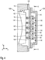
- FIG. 4 A second embodiment 136b of the optical manipulator 136 is shown with a deformable concave mirror 70, as shown for example in US Pat JP 2013-106014 is disclosed.
- the mirror 70 is of
- the optical manipulator 136b includes a manipulation device 138 with a plurality of actuators 140.
- the actuators 140 are fixed to a support plate 160 and act on mirror posts 164, which at the Rear side 142 of the mirror 70 are fixed and extending in the Y direction through recesses 162 in the support plate 160.
- the actuators 140 exert a force in the X and Z directions, ie parallel to the rear side 142 of the mirror 70, and thus laterally on the mirror posts 164, thus causing a local deformation of the reflective coating 144 of the mirror 70.
- the optical manipulator contains 136b, a housing 148 on which position sensors 166 for determining the XZ deflection of the mirror posts 164 are arranged.
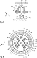
- Fig. 5 shows an actuator 140 of the optical manipulator 136 after Fig. 4 in a detailed schematic view.
- the actuator 140 includes a drive member 152.
- the drive member 152 is fixed to the support plate 160 and may expand or contract in the Y direction.
- a moving end of the drive member 152 acts on an arm of an L-shaped lever 168 which is pivotally attached to the support plate 160.
- Another arm of the lever 168 thereby moves in the X direction in this actuator 140 and acts on the mirror post 164 via a connecting member 170.
- the mirror post 164 is biased by a spring 172 and extends through the recess in the direction of mirror 70.
- With a fastener 174 of the mirror post 164 is attached to a protruding from the back 142 portion 176 of the mirror 70.
- the actuator 140 includes a further drive element, a correspondingly arranged lever with a connecting element and a further spring.
- Fig. 6 shows a cross section of the optical manipulator 136b according to Fig. 4 along the line AA in Fig. 4 , It can be clearly seen that each actuator 140 each having a spring 172 and a drive element 152 for a deflection of the mirror post 164 in the X direction and in the Z direction. The actuators are arranged partially symmetrical to the optical axis 158 of the mirror 70 at the rear side 142 thereof. Each actuator 140 can be individually driven and causes a local deformation of the reflective coating 144 of the mirror 70. These local areas in the actuators 140 represent separately in their optical action adjustable zones 146 of the optical manipulator 136b.
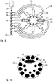
- FIG. 7 A third exemplary embodiment 136c of an optical manipulator 136 with a deformable concave mirror 70 is shown in a schematic cross section.
- the optical manipulator 136c contains, under a reflective coating 144, a piezoelectric layer 180 with which local deformation of the reflective coating 144 can be effected by local application of an electrical voltage.
- Such an optical manipulator 136c is used in the DE 10 2011 081 603 A1 described.
- the optical manipulator 136c includes a concave shaped substrate 182 on which a plurality of electrical leads 184 are disposed.
- FIG. 8 FIG. 10 shows a top view of an exemplary arrangement of the electrical leads 184 on the substrate 182.
- Each electrical lead 184 includes a first contact surface 185 proximate the periphery of the substrate 182.
- each electrical lead 184 includes a second contact surface 186 which, at a via in FIG an insulating layer 190 provided over the electrical leads 184 is arranged.
- the insulation layer 190 carries a layer of areal control electrodes 192 which are each electrically connected to the corresponding electrical line 184 via a via 188.
- the piezoelectric layer 180 is arranged, which in turn carries a counter electrode 194.
- the counter electrode 194 extends over the entire piezoelectric layer 180 and carries a protective layer 196.
- the protective layer 196 finally the reflective coating 144 is arranged.
- the in Fig. 1 illustrated thermal manipulator 236 with an infrared light irradiation of local areas of the lens 28 includes a plurality of irradiation units 238, which radiate from an infrared light source 240 provided infrared light each with an adjustable intensity to a specific area or a zone of the lens 28.
- the thermal manipulator 236 can be arranged in a field or pupil plane of the projection objective 22 or intermediately, ie between field and pupil plane.
- a thermal manipulator 236, which irradiates infrared light to a specific area or a zone of the lens 28, is suitable in particular for electromagnetic exposure radiation in the deep ultraviolet spectral range (DUV) or in the VUV spectral range.
- DUV deep ultraviolet spectral range
- FIG. 9 an embodiment of such a thermal manipulator 236 is shown schematically, as shown for example in the US 2008/0204682 A1 is disclosed.
- the infrared light source 240 generates infrared radiation 244 as heating radiation.
- the IR radiation 244 propagates in the direction of a photoelectronic sensor 245.
- a plurality of pivotable deflection mirrors 248 is arranged one behind the other. In a first rotational position, a respective one of the pivotable deflecting mirrors 248 is located outside the beam path of the IR radiation 244 and can be passed in the direction of the photoelectric sensor 245.
- each of the deflection mirrors 248 deflects the IR radiation 244 in such a way that it is coupled into a respective optical waveguide 250.
- the IR radiation 244 led to an irradiation unit 238.
- a deflection mirror 248 and an optical waveguide 250 are provided for each irradiation unit 238, a deflection mirror 248 and an optical waveguide 250 are provided.
- the IR radiation 244 first passes through a first condenser lens 252 and then a beam splitter 254.
- the beam splitter 254 directs a small portion of the IR radiation 244 onto a photoelectric sensor 256
- IR radiation 244 exits the irradiation unit 238 through a second condenser lens 258 and irradiates a certain area of the lens 28.
- all the irradiation units 238 are held aligned by a suitably formed holder 260.
- the intensity of the irradiation and thus the temperature increase is directly dependent on the duration and frequency for each area or zone on the lens 28, with which the respective deflection mirror 248 couples the IR radiation 244 into the corresponding optical waveguide 250.
- the intensity of the IR radiation can be detected by the photoelectric sensors 256 for each zone.
- Fig. 10 shows a schematic view of the irradiation of the lens 28 by the irradiation units 238 according to Fig. 9 for generating a temperature distribution with different temperatures in different local zones 246 of the lens 28. Large circles symbolize a high intensity of the irradiation and smaller circles a lower intensity. Also shown is an exemplary cross-section 264 of the exposure beam path 48, which is asymmetric in the illustrated case.
- the exposure radiation also leads to a, in this case, undesired, temperature increase in the region of the cross section 264. Temperature increases cause the temperature-dependent optical properties of the lens material, such as the refractive index, to change.
- suitable irradiation of the lens 28 with the irradiation units 2308 changes in the optical properties of the lens 28 induced by the exposure radiation can be compensated.
- the optical manipulator 336 is designed as a current-heated or thermally-driven thermal manipulator and contains as optical elements a transparent first optical disk 338 and a transparent second optical disk 340.
- the optical disks 338, 340 are perpendicular to the optical axis 34 in the optical path of the Projection lens 22 arranged and can be heated locally via very small electrically conductive and ohmic structures. Between the optical plates 338, 340, a gap 342 is formed through which an air flow 344 is guided for cooling.
- Fig. 11 shows the first optical disk 338 in a schematic view.
- the plate 338 includes a two-dimensional array of separately heatable zones 346.
- the first optical plate 338 has a 14x14 matrix of zones 346.
- Ninety-six separately heatable zones 346 are optically effectively arranged in the beam path 48 of the projection lens 22.
- the second optical plate 340 is designed accordingly, so that the optical manipulator 336 has a total of one hundred and ninety-two heatable zones 346 in the beam path 48.
- a different number, arrangement and shape of the zones 346 is possible, for example, the zones may be arranged radially or formed as a strip or circular arc.
- the first optical disk 338 has a matrix with at least 5x5 zones, in particular a matrix with at least 10x10 zones, for example a matrix with 10x10 zones or a matrix with 21x21 zones.
- zones 346 always takes place so that compared to the ambient temperature colder and warmer areas compensate in total.
- zones 346 at the edge of the optical disks 338, 340 are actively heated to ambient temperature with thermal contact with other components of the projection lens 22. In this way, a thermal neutrality of the optical manipulator 336 is ensured.
- the optical disks 338, 340 of the optical manipulator 336 are formed in this embodiment as a plane-parallel quartz plates.
- the optical manipulator may be e.g. only one optical disk, more than two optical disks, non-plane parallel disks or one or more lenses or the like with a plurality of heatable zones included.
- the optical manipulator 336 further includes an actuator 350 for setting a predetermined temperature profile for both optical disks 338, 340.
- a temperature profile gives for each zone 346 of both optical disks 338, 340 temperature values or corresponding values, such as a heat output in W / m 2 as a travel.
- the temperature profiles thus represent travel vectors.
- the actuation device 350 supplies each zone 346 of the optical manipulator 336 with a corresponding heating current for setting the predetermined travel vector and can additionally control the cooling by the air flow 344.
- the projection exposure apparatus 10 further includes a manipulator controller 52 for controlling one or more of the optical manipulators 136, 236 and 336 to compensate for wavefront errors that occur or change during operation.
- the manipulator control 52 comprises a present wavefront error determination module 54 and a travel path generator 56 for generating a travel path vector suitable for correcting the present wavefront error.
- the generated Stellwegwegvektor can next to travel for one or more of in Fig. 1 illustrated optical manipulators 136, 236 and 336 also include travel paths for other manipulators of the projection exposure system 10, for example, for not in Fig. 1 Positioning devices or deformation devices of optical elements 28 of the projection lens 22 are shown below.
- the generation of a travel vector is illustrated below using the example of the optical manipulator 336 with reference to FIGS Fig. 11 illustrated optical disk 338 described.
- the described principle can be analogously transferred to the generation of a travel vector for the optical manipulator 136, the optical manipulator 236 or another optical manipulator.
- the determination module 54 either performs a measurement to determine a currently present wavefront error or performs extrapolation based on previously measured wavefront errors and other parameters such as ambient pressure and the like. Such extrapolation can also be done, for example, based on previously measured wavefront errors as well as a model that predicts lens heating or mirror heating.
- the measurement of a wavefront error takes place, in particular, interferometrically with a wavefront sensor 58, which is integrated into the positioning device 32.
- An apparatus for the interferometric determination of wavefronts is eg in the US 2002/0001088 A1 described.
- the displacement generator 56 generates, according to one embodiment, based on the Zernike coefficients or other suitable parameters of a measured or extrapolated wavefront error, a travel vector with travel ranges for each zone 346 of the optical manipulator 336 and for further manipulators of the projection exposure tool 10, such as for each zone 146 of the optical Manipulator 136 or for each zone 246 of the optical manipulator 236.
- the Stellwegvektor is thereby configured by Stellweggenerator such that the wavefront of the projection lens 22 is approximated to a desired wavefront.
- the desired wavefront may be defined by spherical wavefronts present at the individual field points in the image plane 26, the envelope of these wavefronts along the image plane 26 giving a planar wavefront. Such a desired wavefront is referred to in the context of this application as a reference wavefront.
- the approximation of the actual wavefront to the reference wavefront means a minimization of the wavefront error of the projection objective 22.
- the desired wavefront, to which the wavefront of the projection objective 22 is approximated using the travel vector is defined by a wavefront deviating from the reference wavefront.
- a deliberately deviating desired wavefront can be determined by means of the so-called imaging enhancement method.
- adjusted wavefront deviations are specifically determined for the mask structures to be imaged in the individual case, which make it possible to image the corresponding mask structures with a higher resolution.
- the generation of the travel vector is carried out by an adjustment algorithm generating the optimization algorithm, for example, based on basic functions for each zone 346 with a 3x3 matrix, 5x5 matrix or 7x7 matrix to account for a Heat conduction into adjacent zones 346 is based.
- the optimization algorithm can be based on algorithms known to those skilled in the art, eg, singular value decomposition (SVD) or Tikhonov regularization.
- the thermal neutrality of the optical manipulator 336 leads to a very complex optimization problem, which in itself can not be solved in real time during the exposure operation of the projection exposure apparatus 10 as a rule. Therefore, 56 previously determined Stellwegvektoren for certain wavefront errors, for example for certain Zernike coefficients are stored in a memory 60 of the Stellweggenerators. These are taken into account when generating a travel path from the optimization algorithm for solving the optimization problem. In this way, a Stellweggeneration by the Stellweggenerator 56 in real time during the exposure operation of the projection exposure apparatus 10 is possible.
- the projection exposure apparatus 10 furthermore contains a zone checking unit 62 for checking the functioning of each zone 346 of the optical manipulator 336.
- the zone checking unit 62 checks whether the adjustment paths and therefore the temperature within each zone 346 can be set within a predetermined nominal setting range.
- a cause for a travel restriction in the heatable zones 346 may be a faulty Gleichsciens the control signals of two adjacent zones 346a, 346b in the form of an electrical short circuit between the two adjacent zones 346a, 346b. As a result, both zones 346a, 346b are always operated with the same heating power. Only a single travel for zones 346a, 346b can be set.
- Another cause for a travel restriction may be a faulty resistance characteristic of a zone 346c occurring during operation or already present prior to startup. The out-of-tolerance resistance characteristic can in particular lead to a limited travel range.
- the zone check unit 62 detects a short circuit between the zones 346a, 346b, it provides a uniform travel as a restriction parameter for the shorted zones 346a, 346b. This applies analogously to that with reference to the in Fig. 7 If the zone check unit 62 detects a restricted travel range due to a faulty resistance characteristic, it sets a maximum allowable travel as a restriction parameter for the failed zone 346b.
- the zone check unit 62 may be configured to appropriately test the actuator characteristic of each zone of the deformable mirror 70. Also, the zone check unit 62 may be configured to check the actuator characteristic of each zone of the optical manipulator 236 with infrared heating.
- Travel restrictions due to defective zones 346a, 346b, 346c result in a generated travel vector with a not fully executable travel for one or more of these zones 346a, 346b, 346c to a faulty setting of the optical manipulator 336 and thus to a poor compensation of an existing wavefront error , New wavefront errors can also be induced.
- An adaptation of the optimization algorithm for the actuating path generation to the travel restrictions would be associated with a very large amount of time.
- the large amount of time required for adapting the optimization algorithm to the travel restrictions is due, in particular, to the fact that the travel vectors used by the optimization algorithm, which are predetermined for specific wavefront errors no longer have any validity and would have to be completely redetermined by time-consuming solution of a complex optimization problem.
- a checking device 64 of the projection exposure apparatus 10 therefore first determines whether a restriction parameter is available for one or more zones 346 is predetermined and then checked for each generated travel vector the travel paths for zones 346a, 346b, 346c with predetermined restriction parameters on feasibility. If the verification device 64 determines a non-executable travel for one or more of the zones with a predetermined restriction, a corresponding correction of the generated travel vector is triggered. Examples of incompletely executable travel paths are, for example, different travel paths for the short-circuited zones 346a, 346b or an adjustment path beyond the restricted travel range for the faulty zone 346c. In addition, with each generated travel vector, the checking device 64 can check all travel paths for fully functional zones 346 for compliance with the nominal travel range.
- the checking device 64 can check the travel ranges that are valid with respect to the zones 146 and 246, respectively, for compliance with the corresponding desired travel range.
- the zone checking unit 62 and the checking device 64 can also be combined to form a so-called checking device.
- the projection exposure apparatus 10 further includes a correction device 66 for correcting the generated travel vector in the presence of one or more incompletely executable travel paths.
- the correction device 66 first checks whether a correction value vector for the one or more non-executable travel paths is already present in a memory 68. If one exists, it will be used to correct the generated travel vector.
- the correction device 66 checks whether there is a base correction vector in the memory 68 for the restriction and the zone or zones specified by the restriction parameter.
- the base correction vector represents a correction value vector for a base disturbance with respect to the zone and the present constraint. If a base correction vector is present, the correction device 66 determines a suitable scaling factor on the basis of the generated travel vector, in particular the one or more non-executable travel paths. Subsequently, the correction device 66 calculates the correction value vector by scaling the base correction vector with the determined scaling factor. In addition, the correction device can be designed to calculate a base correction vector.
- Both the correction value vector and the base correction vector contain values for all travel paths of the generated travel vector.
- the correction device 66 By adding the respective correction value of the correction value vector to the corresponding travel of the generated travel vector, the correction device 66 generates a corrected travel vector.
- the actuation device 50 sets the heating power for all zones 346 of the optical manipulator 336 in accordance with the adjustment paths of the corrected manipulated variable vector. In this way, in the case of the optical manipulator 336, despite one or more defective zones, the optical effect predefined by the generated travel vector is set. In the case of the other manipulators of the projection exposure apparatus 10, such as the optical manipulator 136 or the optical manipulator 236, an adjustment takes place in accordance with corresponding travel ranges of the corrected travel vector.
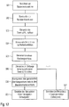
- Fig. 12 a flow chart illustrating a first embodiment of the method for controlling the projection exposure apparatus 10 is shown.
- the method is used to control the projection exposure apparatus 10 in the presence of an electrical short between two adjacent zones 346a, 346b of the current-heated optical manipulator 336. Due to the short circuit, both zones 346a, 346b can only be operated with the same heating power or the same travel.
- the method can thus also be applied to other manipulators having a plurality of separately adjustable zones and a disordered uniform travel for two adjacent zones, e.g. at the manipulator 136 with an adaptive mirror 70 or at the manipulator 236 with a heating by infrared light.
- a base correction vector for a short circuit takes place in a computer. For example, short circuits between certain zones 346 may be excluded or more likely than others due to the structure of the tracks .
- a base difference between the two zones 346 involved is first determined. For example, for the first zone, the average value of the setpoint travel range is used as the travel range, and the maximum possible travel range is used for the second zone.
- travel paths for all other zones 346 are determined by solving the following optimization problem: maintaining the specified maximum adjustment ranges for all other zones 346 of both optical disks 338, 340, setting the predetermined values for the first and second zones according to the base difference, and minimum Aberration by the two optical disks 338, 340.
- the positioning capabilities of other manipulators of the projection exposure apparatus 10 can be taken into account.
- the Base correction vector then also contains correction values for the other manipulators.
- a quadratic programming algorithm for example, a quadratic programming algorithm (QuadProg), sequential quadratic programming (SQP: Sequential Quadratic Programming), Tikhonov regularization and / or Hansen L-curve method can be used.
- base differences such as a difference formed around the mean of the target travel range, such as -1 W / m 2 for the first zone and +1 W / m 2 for the second zone may be used.
- a difference formed around the mean of the target travel range such as -1 W / m 2 for the first zone and +1 W / m 2 for the second zone
- the base correction vector thus determined can be used directly as a correction value vector using the average value (s1 + s2) / 2 as the travel range for the first and second zones. With these specifications, a correction value vector can thus also be calculated directly.
- the travel ranges thus determined for the other zones 346 compensate for the optical effect of the predetermined travel ranges for the first and second zones. Conversely, the travel paths of the other zones with the same travel for the first and second zones induce an optical effect, which corresponds to the non-adjustable due to the short circuit base difference.
- the determined base correction vector can be adjusted by appropriately scaling for other differences between the first and second zones.
- the determined base correction values for the projection exposure apparatus 10 are provided in the memory 68 of the projection exposure apparatus 10. They can thus be used immediately after the occurrence of a short circuit for a correction of the generated travel vector. Alternatively, the base correction values may also be stored in another memory and provided over a network.
- the zone checking unit 62 sets a uniform adjustment path as a restriction parameter for the short-circuited zones 346a, 346b.
- the correction of generated travel vectors is activated.
- the calculation of the base correction vector can take place only now, for example by the correction device 66.
- a measurement or an extrapolation of the currently present wavefront error by the determination module 54 is carried out during the operation of the projection exposure apparatus 10.
- the measured or extrapolated wavefront error is then forwarded to the Stellweggenerator 56.
- a generation S05 of a travel vector with travel paths for each zone 346 of the optical manipulator 336 and for further manipulators of the projection exposure system 10 by the Stellweggenerator 56 is generated. Generating the travel is based on the measured or extrapolated instantaneous wavefront error of the projection lens 22 in the above described Wise.
- a sixth step S06 the checking device 64 first determines whether there is a restriction parameter relating to a short circuit between two zones 346. If a short circuit for two zones 346a, 346b is specified, then a check of the adjustment paths generated for the short-circuited zones 346a, 346b for equality by the checking device 64 takes place.
- correction of the generated travel vector is effected by the correction device 66.
- the base correction vector for the short-circuited zones 346a, 346b provided in the memory 68 is determined.
- the nominal value corresponds to that used for the calculation of the base correction vector based Period.
- the correction value vector is determined.
- a corrected travel vector is calculated by component-wise adding the correction values of the correction value vector to the travel paths of the generated travel vector.
- the travel value in the corrected travel vector is either the average value (s1 + s2) / 2 of the generated travel ranges for a base difference of travel ranges around the mean value of the desired travel range, or the generated travel for the first region 346a at a base difference from the mean value and the maximum value of the set travel range.
- step S09 an adjustment of all zones 346 of the optical manipulator 336 and also of other manipulators of the projection exposure apparatus 10 takes place corresponding to the adjustment paths of the corrected adjustment path vector for compensation of the measured or extrapolated wavefront error.
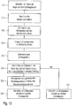
- Fig. 13 a flow chart illustrating a second embodiment of the method for controlling the projection exposure apparatus 10 is shown.
- the method is used to control the projection exposure apparatus 10 in the presence of a defective zone 346c with an out of tolerance resistance characteristic.
- a limited travel range of the zone 346c is caused, whereby certain generated travel paths for the zone 346c are not completely executable.
- the method can thus also be applied to other manipulators with a plurality of separately adjustable zones and a faulty zone with limited travel range, such as manipulator 136 with an adaptive mirror or manipulator 236 with heating by infrared light.
- a check of all takes place already during the production of the optical disks 338, 340 or the optical manipulator 336 Zones 346 on the presence of a limited Stellweg Suites due to a lying outside the desired range resistance characteristic.
- a calculation of a base correction vector for the faulty zone 346c takes place in a second step S12.
- a maximum correction travel is first determined.
- the non-executable portion of a maximum nominal travel is defined as the maximum correction travel.
- maximum travel ranges are set by both optical disks 338, 340, eg +/- 20 W / m 2 and +/- 0.1 K for each zone.
- travel paths for all other zones 346 are determined by solving the following optimization problem: maintaining the specified maximum adjustment ranges for all other zones 346 of both optical disks 338, 340, setting the maximum correction travel for the defective zone 346c, and minimum aberration through the two optical ones Plates 338, 340.
- the base correction vector then also contains correction values for the other manipulators.
- a quadratic programming algorithm for example, a quadratic programming algorithm (QuadProg), sequential quadratic programming (SQP: Sequential Quadratic Programming), Tikhonov regularization and / or Hansen L-curve method can be used.
- the adjustment paths of the base correction vector thus determined generate an optical effect of the optical manipulator 336, which corresponds to the non-executable portion of a maximum travel range for the faulty zone.
- the base correction vector can be adjusted by appropriate scaling to other incompletely executable travel paths for the faulty zone 346c.
- a third step S13 the optical manipulator 336 is provided together with the determined basic correction vector for the projection exposure apparatus.
- the basic correction vector is stored in the memory 68 of the projection exposure apparatus 10.
- a restricted, maximum possible adjustment path for the zone 346c is set as the restriction parameter. This can e.g. be performed by the zone check unit 62. There is thus an activation of the correction of generated travel vectors.
- a check is first made for the presence of a restriction parameter with a restricted maximum travel for a zone 346 by the checking device 64. If there is a restriction regarding the maximum travel for a zone 346c, then a check is made for the faulty zone 346c generated travel path vector to exceed the limited maximum travel for zone 346c instead.
- the generated travel vector is corrected by the correction device 66.
- S18 Memory 68 provided base correction vector for the faulty zone 346c determined.
- the nominal value corresponds to the maximum correction travel used in the calculation of the base correction vector.
- a corrected travel vector is calculated by component-wise adding the correction values of the correction value vector to the manipulated values of the generated travel vector.
- the limited maximum travel is determined as the travel in the corrected travel vector.
- step S19 all zones 346 of the optical manipulator 336 and also other manipulators of the projection exposure apparatus 10 are adjusted in accordance with the adjustment paths of the corrected adjustment path vector for compensation of the measured or extrapolated wavefront error.
- the basic correction vectors calculated after step S12 can also be used in a further exemplary embodiment of the method for compensating a travel path cutoff as a result of an override by a generated travel that exceeds the maximum target travel path.
- a check of all travel paths of the generated travel path vector takes place on exceeding the maximum nominal travel travel. If there is an overshoot, a basic correction vector for the affected zone 346 is determined analogously to step S18, a scaling factor is determined and a correction value vector is calculated.
- the maximum nominal travel is now used instead of the restricted maximum travel. Subsequently, an adjustment of all zones 346 of the optical manipulator 336 and further manipulators according to step S19.
Landscapes
- Physics & Mathematics (AREA)
- General Physics & Mathematics (AREA)
- Optics & Photonics (AREA)
- Exposure And Positioning Against Photoresist Photosensitive Materials (AREA)
- Exposure Of Semiconductors, Excluding Electron Or Ion Beam Exposure (AREA)
- Mounting And Adjusting Of Optical Elements (AREA)
Applications Claiming Priority (1)
| Application Number | Priority Date | Filing Date | Title |
|---|---|---|---|
| DE102015201020.1A DE102015201020A1 (de) | 2015-01-22 | 2015-01-22 | Projektionsbelichtungsanlage mit Manipulator sowie Verfahren zum Steuern einer Projektionsbelichtungsanlage |
Publications (3)
| Publication Number | Publication Date |
|---|---|
| EP3048486A2 EP3048486A2 (de) | 2016-07-27 |
| EP3048486A3 EP3048486A3 (de) | 2016-08-31 |
| EP3048486B1 true EP3048486B1 (de) | 2018-06-06 |
Family
ID=55174529
Family Applications (1)
| Application Number | Title | Priority Date | Filing Date |
|---|---|---|---|
| EP16000098.0A Active EP3048486B1 (de) | 2015-01-22 | 2016-01-15 | Projektionsbelichtungsanlage mit manipulator sowie verfahren zum steuern einer projektionsbelichtungsanlage |
Country Status (4)
| Country | Link |
|---|---|
| US (1) | US9760019B2 (enExample) |
| EP (1) | EP3048486B1 (enExample) |
| JP (1) | JP6266028B2 (enExample) |
| DE (1) | DE102015201020A1 (enExample) |
Families Citing this family (15)
| Publication number | Priority date | Publication date | Assignee | Title |
|---|---|---|---|---|
| DE102013204391B3 (de) | 2013-03-13 | 2014-05-28 | Carl Zeiss Smt Gmbh | Projektionsobjektiv mit Wellenfrontmanipulator |
| KR101668984B1 (ko) * | 2013-09-14 | 2016-10-24 | 칼 짜이스 에스엠티 게엠베하 | 마이크로리소그래피 투영 장치의 동작 방법 |
| DE102017208364A1 (de) * | 2017-05-18 | 2018-11-22 | Carl Zeiss Smt Gmbh | Optisches system sowie verfahren |
| DE102019219289A1 (de) | 2019-12-11 | 2021-06-17 | Carl Zeiss Smt Gmbh | Optisches System, sowie Heizanordnung und Verfahren zum Heizen eines optischen Elements in einem optischen System |
| DE102020201723A1 (de) | 2020-02-12 | 2021-08-12 | Carl Zeiss Smt Gmbh | Projektionsbelichtungsanlage mit einem thermischen Manipulator |
| JP7486335B2 (ja) * | 2020-03-30 | 2024-05-17 | キヤノン株式会社 | インプリント装置、インプリント方法、および物品製造方法 |
| DE102020207752A1 (de) | 2020-06-23 | 2021-12-23 | Carl Zeiss Smt Gmbh | Heizanordnung und Verfahren zum Heizen eines optischen Elements |
| DE102020207748A1 (de) * | 2020-06-23 | 2021-03-25 | Carl Zeiss Smt Gmbh | Optisches System, insbesondere in einermikrolithographischen Projektionsbelichtungsanlage |
| JP2022022911A (ja) * | 2020-07-10 | 2022-02-07 | キヤノン株式会社 | 結像光学系、露光装置、および物品製造方法 |
| DE102020209784A1 (de) * | 2020-08-04 | 2022-02-10 | Carl Zeiss Smt Gmbh | Verfahren zur herstellung oder einstellung einer projektionsbelichtungsanlage |
| US12321099B2 (en) * | 2021-08-30 | 2025-06-03 | Taiwan Semiconductor Manufacturing Company, Ltd. | Method for generating EUV radiation |
| DE102022204015A1 (de) | 2022-04-26 | 2023-10-26 | Carl Zeiss Smt Gmbh | Aktuator und Deformationsspiegel |
| DE102022114974A1 (de) | 2022-06-14 | 2023-12-14 | Carl Zeiss Smt Gmbh | Verfahren zum Heizen eines optischen Elements sowie optisches System |
| DE102022116700A1 (de) * | 2022-07-05 | 2024-01-11 | Carl Zeiss Smt Gmbh | Optische Baugruppe, Projektionsbelichtungsanlage für die Halbleiterlithographie und Verfahren |
| DE102022212380A1 (de) | 2022-11-21 | 2023-11-23 | Carl Zeiss Smt Gmbh | Verfahren und Vorrichtung zum Heizen eines EUV-Spiegels, mikrolithographische Projektionsbelichtungsanlage |
Family Cites Families (23)
| Publication number | Priority date | Publication date | Assignee | Title |
|---|---|---|---|---|
| TW550377B (en) | 2000-02-23 | 2003-09-01 | Zeiss Stiftung | Apparatus for wave-front detection |
| US6398373B1 (en) * | 2000-08-09 | 2002-06-04 | Asml Us, Inc. | Pneumatic control system and method for shaping deformable mirrors in lithographic projection systems |
| DE10046379A1 (de) * | 2000-09-20 | 2002-03-28 | Zeiss Carl | System zur gezielten Deformation von optischen Elementen |
| DE10146499B4 (de) * | 2001-09-21 | 2006-11-09 | Carl Zeiss Smt Ag | Verfahren zur Optimierung der Abbildungseigenschaften von mindestens zwei optischen Elementen sowie Verfahren zur Optimierung der Abbildungseigenschaften von mindestens drei optischen Elementen |
| US6803994B2 (en) | 2002-06-21 | 2004-10-12 | Nikon Corporation | Wavefront aberration correction system |
| US8111378B2 (en) | 2004-02-13 | 2012-02-07 | Nikon Corporation | Exposure method and apparatus, and device production method |
| DE102004035595B4 (de) | 2004-04-09 | 2008-02-07 | Carl Zeiss Smt Ag | Verfahren zur Justage eines Projektionsobjektives |
| US7423765B2 (en) * | 2004-07-31 | 2008-09-09 | Carl Zeiss Smt Ag | Optical system of a microlithographic projection exposure apparatus |
| US20080204682A1 (en) | 2005-06-28 | 2008-08-28 | Nikon Corporation | Exposure method and exposure apparatus, and device manufacturing method |
| DE102006045075A1 (de) | 2006-09-21 | 2008-04-03 | Carl Zeiss Smt Ag | Steuerbares optisches Element |
| US20100033704A1 (en) * | 2008-08-11 | 2010-02-11 | Masayuki Shiraishi | Deformable mirror, mirror apparatus, and exposure apparatus |
| DE102008042356A1 (de) * | 2008-09-25 | 2010-04-08 | Carl Zeiss Smt Ag | Projektionsbelichtungsanlage mit optimierter Justagemöglichkeit |
| WO2011074319A1 (ja) | 2009-12-14 | 2011-06-23 | 株式会社ニコン | デフォーマブルミラー、照明光学系、露光装置、およびデバイス製造方法 |
| WO2012013751A1 (en) | 2010-07-30 | 2012-02-02 | Carl Zeiss Smt Gmbh | Euv exposure apparatus |
| DE102011077784A1 (de) | 2011-06-20 | 2012-12-20 | Carl Zeiss Smt Gmbh | Projektionsanordnung |
| DE102011081603A1 (de) | 2011-08-26 | 2012-10-25 | Carl Zeiss Smt Gmbh | Adaptiver Spiegel und Verfahren zu dessen Herstellung |
| JP2013106014A (ja) | 2011-11-16 | 2013-05-30 | Nikon Corp | 変形可能な反射光学素子及びその駆動方法、光学系、並びに露光装置 |
| JP5861973B2 (ja) * | 2012-02-04 | 2016-02-16 | カール・ツァイス・エスエムティー・ゲーエムベーハー | マイクロリソグラフィ投影露光装置を作動させる方法及びそのような装置の投影対物系 |
| JP2013161992A (ja) | 2012-02-06 | 2013-08-19 | Nikon Corp | 変形可能な反射光学素子、光学系、及び露光装置 |
| DE102012205096B3 (de) * | 2012-03-29 | 2013-08-29 | Carl Zeiss Smt Gmbh | Projektionsbelichtungsanlage mit mindestens einem Manipulator |
| DE102012212757A1 (de) * | 2012-07-20 | 2014-01-23 | Carl Zeiss Smt Gmbh | Verfahren zum betreiben einer mikrolithographischen projektionsbelichtungsanlage |
| US9651872B2 (en) | 2013-03-13 | 2017-05-16 | Carl Zeiss Smt Gmbh | Projection lens with wavefront manipulator |
| DE102013204391B3 (de) * | 2013-03-13 | 2014-05-28 | Carl Zeiss Smt Gmbh | Projektionsobjektiv mit Wellenfrontmanipulator |
-
2015
- 2015-01-22 DE DE102015201020.1A patent/DE102015201020A1/de not_active Ceased
-
2016
- 2016-01-15 EP EP16000098.0A patent/EP3048486B1/de active Active
- 2016-01-20 JP JP2016009061A patent/JP6266028B2/ja active Active
- 2016-01-21 US US15/002,564 patent/US9760019B2/en active Active
Non-Patent Citations (1)
| Title |
|---|
| None * |
Also Published As
| Publication number | Publication date |
|---|---|
| EP3048486A2 (de) | 2016-07-27 |
| US9760019B2 (en) | 2017-09-12 |
| DE102015201020A1 (de) | 2016-07-28 |
| US20160216616A1 (en) | 2016-07-28 |
| JP6266028B2 (ja) | 2018-01-24 |
| EP3048486A3 (de) | 2016-08-31 |
| JP2016136253A (ja) | 2016-07-28 |
Similar Documents
| Publication | Publication Date | Title |
|---|---|---|
| EP3048486B1 (de) | Projektionsbelichtungsanlage mit manipulator sowie verfahren zum steuern einer projektionsbelichtungsanlage | |
| DE102012205096B3 (de) | Projektionsbelichtungsanlage mit mindestens einem Manipulator | |
| DE102015206448B4 (de) | Steuerungsvorrichtung zur Steuerung mindestens eines Manipulators eines Projektionsobjektives, Justieranlage und Verfahren zum Steuern mindestens eines Manipulators | |
| EP2621662B1 (de) | Vorrichtung und verfahren für die bearbeitung von material mit fokussierter elektromagnetischer strahlung | |
| WO2021160583A1 (de) | Projektionsbelichtungsanlage mit einem thermischen manipulator | |
| EP4133589B1 (de) | Verfahren, ansteuereinrichtung, optisches system und lithographieanlage | |
| DE102017217695A1 (de) | Verfahren zum Modifizieren des Deformationsverhaltens eines deformierbaren Spiegels | |
| DE102014206765A1 (de) | Spiegelanordnung, Projektionsobjektiv und EUV-Lithographieanlage | |
| DE102015220537A1 (de) | Projektionsbelichtungsanlage mit mindestens einem Manipulator | |
| WO2021224036A1 (de) | Verfahren zum betreiben eines deformierbaren spiegels, sowie optisches system mit einem deformierbaren spiegel | |
| WO2012041589A1 (de) | Projektionsbelichtungsanlage mit optimierter justagemöglichkeit | |
| WO2023099308A1 (de) | Verfahren zum erzeugen einer lokalen dickenänderung einer beschichtung, spiegel und euv-lithographiesystem | |
| DE102006039895A1 (de) | Verfahren zur Korrektur von durch Intensitätsverteilungen in optischen Systemen erzeugten Abbildungsveränderungen sowie entsprechendes optisches System | |
| DE102012213794A1 (de) | Maskeninspektionsverfahren und Maskeninspektionssystem für EUV-Masken | |
| DE102018215727A1 (de) | Projektionsbelichtungsanlage mit einem kompaktierten optischen Element | |
| DE102020131389B4 (de) | Projektionsbelichtungsanlage und Verfahren zur Korrektur von Temperatureinflüssen durch Beeinflussung der Oberflächenform eines optischen Elements | |
| DE102021211975A1 (de) | Verfahren zur Nachbildung einer Ziel-Wellenfront eines abbildenden optischen Produktions-Systems sowie Metrologiesystem zur Durchführung des Verfahrens | |
| WO2022156926A1 (de) | Verfahren sowie vorrichtung zum bestimmen des erwärmungszustandes eines optischen elements in einem optischen system | |
| DE102008006687A1 (de) | Verfahren zum Verbessern von Abbildungseigenschaften eines optischen Systems sowie optisches System | |
| WO2021140157A1 (de) | Verfahren zur kompensation einer bewegung und projektionsbelichtungsanlage für die halbleiterlithographie | |
| WO2024256376A1 (de) | Verfahren zur herstellung eines projektionsobjektivs, projektionsobjektiv, projektionsbelichtungsanlage und projektionsbelichtungsverfahren | |
| WO2024227706A2 (de) | Verfahren zum auswerten von messwerten einer aberration eines projektionsobjektivs | |
| EP4445220A1 (de) | Verfahren zum kalibrieren eines manipulierbaren optischen moduls | |
| DE102024204314A1 (de) | Verfahren zum Herstellen eines Spiegels | |
| DE102024201765A1 (de) | Verfahren zum Betreiben einer Projektionsbelichtungsanlage für die Mikrolithographie |
Legal Events
| Date | Code | Title | Description |
|---|---|---|---|
| PUAI | Public reference made under article 153(3) epc to a published international application that has entered the european phase |
Free format text: ORIGINAL CODE: 0009012 |
|
| AK | Designated contracting states |
Kind code of ref document: A2 Designated state(s): AL AT BE BG CH CY CZ DE DK EE ES FI FR GB GR HR HU IE IS IT LI LT LU LV MC MK MT NL NO PL PT RO RS SE SI SK SM TR |
|
| AX | Request for extension of the european patent |
Extension state: BA ME |
|
| PUAL | Search report despatched |
Free format text: ORIGINAL CODE: 0009013 |
|
| AK | Designated contracting states |
Kind code of ref document: A3 Designated state(s): AL AT BE BG CH CY CZ DE DK EE ES FI FR GB GR HR HU IE IS IT LI LT LU LV MC MK MT NL NO PL PT RO RS SE SI SK SM TR |
|
| AX | Request for extension of the european patent |
Extension state: BA ME |
|
| RIC1 | Information provided on ipc code assigned before grant |
Ipc: G03F 7/20 20060101AFI20160725BHEP |
|
| STAA | Information on the status of an ep patent application or granted ep patent |
Free format text: STATUS: REQUEST FOR EXAMINATION WAS MADE |
|
| 17P | Request for examination filed |
Effective date: 20170228 |
|
| RBV | Designated contracting states (corrected) |
Designated state(s): AL AT BE BG CH CY CZ DE DK EE ES FI FR GB GR HR HU IE IS IT LI LT LU LV MC MK MT NL NO PL PT RO RS SE SI SK SM TR |
|
| GRAP | Despatch of communication of intention to grant a patent |
Free format text: ORIGINAL CODE: EPIDOSNIGR1 |
|
| STAA | Information on the status of an ep patent application or granted ep patent |
Free format text: STATUS: GRANT OF PATENT IS INTENDED |
|
| INTG | Intention to grant announced |
Effective date: 20180104 |
|
| GRAS | Grant fee paid |
Free format text: ORIGINAL CODE: EPIDOSNIGR3 |
|
| GRAA | (expected) grant |
Free format text: ORIGINAL CODE: 0009210 |
|
| STAA | Information on the status of an ep patent application or granted ep patent |
Free format text: STATUS: THE PATENT HAS BEEN GRANTED |
|
| AK | Designated contracting states |
Kind code of ref document: B1 Designated state(s): AL AT BE BG CH CY CZ DE DK EE ES FI FR GB GR HR HU IE IS IT LI LT LU LV MC MK MT NL NO PL PT RO RS SE SI SK SM TR |
|
| REG | Reference to a national code |
Ref country code: GB Ref legal event code: FG4D Free format text: NOT ENGLISH |
|
| REG | Reference to a national code |
Ref country code: CH Ref legal event code: EP Ref country code: AT Ref legal event code: REF Ref document number: 1006766 Country of ref document: AT Kind code of ref document: T Effective date: 20180615 |
|
| REG | Reference to a national code |
Ref country code: IE Ref legal event code: FG4D Free format text: LANGUAGE OF EP DOCUMENT: GERMAN |
|
| REG | Reference to a national code |
Ref country code: DE Ref legal event code: R096 Ref document number: 502016001113 Country of ref document: DE |
|
| REG | Reference to a national code |
Ref country code: NL Ref legal event code: FP |
|
| REG | Reference to a national code |
Ref country code: LT Ref legal event code: MG4D |
|
| PG25 | Lapsed in a contracting state [announced via postgrant information from national office to epo] |
Ref country code: LT Free format text: LAPSE BECAUSE OF FAILURE TO SUBMIT A TRANSLATION OF THE DESCRIPTION OR TO PAY THE FEE WITHIN THE PRESCRIBED TIME-LIMIT Effective date: 20180606 Ref country code: CY Free format text: LAPSE BECAUSE OF FAILURE TO SUBMIT A TRANSLATION OF THE DESCRIPTION OR TO PAY THE FEE WITHIN THE PRESCRIBED TIME-LIMIT Effective date: 20180606 Ref country code: BG Free format text: LAPSE BECAUSE OF FAILURE TO SUBMIT A TRANSLATION OF THE DESCRIPTION OR TO PAY THE FEE WITHIN THE PRESCRIBED TIME-LIMIT Effective date: 20180906 Ref country code: ES Free format text: LAPSE BECAUSE OF FAILURE TO SUBMIT A TRANSLATION OF THE DESCRIPTION OR TO PAY THE FEE WITHIN THE PRESCRIBED TIME-LIMIT Effective date: 20180606 Ref country code: FI Free format text: LAPSE BECAUSE OF FAILURE TO SUBMIT A TRANSLATION OF THE DESCRIPTION OR TO PAY THE FEE WITHIN THE PRESCRIBED TIME-LIMIT Effective date: 20180606 Ref country code: NO Free format text: LAPSE BECAUSE OF FAILURE TO SUBMIT A TRANSLATION OF THE DESCRIPTION OR TO PAY THE FEE WITHIN THE PRESCRIBED TIME-LIMIT Effective date: 20180906 Ref country code: SE Free format text: LAPSE BECAUSE OF FAILURE TO SUBMIT A TRANSLATION OF THE DESCRIPTION OR TO PAY THE FEE WITHIN THE PRESCRIBED TIME-LIMIT Effective date: 20180606 |
|
| PG25 | Lapsed in a contracting state [announced via postgrant information from national office to epo] |
Ref country code: LV Free format text: LAPSE BECAUSE OF FAILURE TO SUBMIT A TRANSLATION OF THE DESCRIPTION OR TO PAY THE FEE WITHIN THE PRESCRIBED TIME-LIMIT Effective date: 20180606 Ref country code: GR Free format text: LAPSE BECAUSE OF FAILURE TO SUBMIT A TRANSLATION OF THE DESCRIPTION OR TO PAY THE FEE WITHIN THE PRESCRIBED TIME-LIMIT Effective date: 20180907 Ref country code: RS Free format text: LAPSE BECAUSE OF FAILURE TO SUBMIT A TRANSLATION OF THE DESCRIPTION OR TO PAY THE FEE WITHIN THE PRESCRIBED TIME-LIMIT Effective date: 20180606 Ref country code: HR Free format text: LAPSE BECAUSE OF FAILURE TO SUBMIT A TRANSLATION OF THE DESCRIPTION OR TO PAY THE FEE WITHIN THE PRESCRIBED TIME-LIMIT Effective date: 20180606 |
|
| PG25 | Lapsed in a contracting state [announced via postgrant information from national office to epo] |
Ref country code: PL Free format text: LAPSE BECAUSE OF FAILURE TO SUBMIT A TRANSLATION OF THE DESCRIPTION OR TO PAY THE FEE WITHIN THE PRESCRIBED TIME-LIMIT Effective date: 20180606 Ref country code: SK Free format text: LAPSE BECAUSE OF FAILURE TO SUBMIT A TRANSLATION OF THE DESCRIPTION OR TO PAY THE FEE WITHIN THE PRESCRIBED TIME-LIMIT Effective date: 20180606 Ref country code: CZ Free format text: LAPSE BECAUSE OF FAILURE TO SUBMIT A TRANSLATION OF THE DESCRIPTION OR TO PAY THE FEE WITHIN THE PRESCRIBED TIME-LIMIT Effective date: 20180606 Ref country code: RO Free format text: LAPSE BECAUSE OF FAILURE TO SUBMIT A TRANSLATION OF THE DESCRIPTION OR TO PAY THE FEE WITHIN THE PRESCRIBED TIME-LIMIT Effective date: 20180606 Ref country code: EE Free format text: LAPSE BECAUSE OF FAILURE TO SUBMIT A TRANSLATION OF THE DESCRIPTION OR TO PAY THE FEE WITHIN THE PRESCRIBED TIME-LIMIT Effective date: 20180606 Ref country code: IS Free format text: LAPSE BECAUSE OF FAILURE TO SUBMIT A TRANSLATION OF THE DESCRIPTION OR TO PAY THE FEE WITHIN THE PRESCRIBED TIME-LIMIT Effective date: 20181006 |
|
| PG25 | Lapsed in a contracting state [announced via postgrant information from national office to epo] |
Ref country code: IT Free format text: LAPSE BECAUSE OF FAILURE TO SUBMIT A TRANSLATION OF THE DESCRIPTION OR TO PAY THE FEE WITHIN THE PRESCRIBED TIME-LIMIT Effective date: 20180606 Ref country code: SM Free format text: LAPSE BECAUSE OF FAILURE TO SUBMIT A TRANSLATION OF THE DESCRIPTION OR TO PAY THE FEE WITHIN THE PRESCRIBED TIME-LIMIT Effective date: 20180606 |
|
| REG | Reference to a national code |
Ref country code: DE Ref legal event code: R097 Ref document number: 502016001113 Country of ref document: DE |
|
| PLBE | No opposition filed within time limit |
Free format text: ORIGINAL CODE: 0009261 |
|
| STAA | Information on the status of an ep patent application or granted ep patent |
Free format text: STATUS: NO OPPOSITION FILED WITHIN TIME LIMIT |
|
| 26N | No opposition filed |
Effective date: 20190307 |
|
| PG25 | Lapsed in a contracting state [announced via postgrant information from national office to epo] |
Ref country code: SI Free format text: LAPSE BECAUSE OF FAILURE TO SUBMIT A TRANSLATION OF THE DESCRIPTION OR TO PAY THE FEE WITHIN THE PRESCRIBED TIME-LIMIT Effective date: 20180606 Ref country code: DK Free format text: LAPSE BECAUSE OF FAILURE TO SUBMIT A TRANSLATION OF THE DESCRIPTION OR TO PAY THE FEE WITHIN THE PRESCRIBED TIME-LIMIT Effective date: 20180606 |
|
| PG25 | Lapsed in a contracting state [announced via postgrant information from national office to epo] |
Ref country code: MC Free format text: LAPSE BECAUSE OF FAILURE TO SUBMIT A TRANSLATION OF THE DESCRIPTION OR TO PAY THE FEE WITHIN THE PRESCRIBED TIME-LIMIT Effective date: 20180606 |
|
| REG | Reference to a national code |
Ref country code: CH Ref legal event code: PL |
|
| PG25 | Lapsed in a contracting state [announced via postgrant information from national office to epo] |
Ref country code: LU Free format text: LAPSE BECAUSE OF NON-PAYMENT OF DUE FEES Effective date: 20190115 |
|
| REG | Reference to a national code |
Ref country code: BE Ref legal event code: MM Effective date: 20190131 |
|
| REG | Reference to a national code |
Ref country code: IE Ref legal event code: MM4A |
|
| PG25 | Lapsed in a contracting state [announced via postgrant information from national office to epo] |
Ref country code: FR Free format text: LAPSE BECAUSE OF NON-PAYMENT OF DUE FEES Effective date: 20190131 |
|
| PG25 | Lapsed in a contracting state [announced via postgrant information from national office to epo] |
Ref country code: BE Free format text: LAPSE BECAUSE OF NON-PAYMENT OF DUE FEES Effective date: 20190131 Ref country code: AL Free format text: LAPSE BECAUSE OF FAILURE TO SUBMIT A TRANSLATION OF THE DESCRIPTION OR TO PAY THE FEE WITHIN THE PRESCRIBED TIME-LIMIT Effective date: 20180606 |
|
| PG25 | Lapsed in a contracting state [announced via postgrant information from national office to epo] |
Ref country code: LI Free format text: LAPSE BECAUSE OF NON-PAYMENT OF DUE FEES Effective date: 20190131 Ref country code: CH Free format text: LAPSE BECAUSE OF NON-PAYMENT OF DUE FEES Effective date: 20190131 |
|
| PG25 | Lapsed in a contracting state [announced via postgrant information from national office to epo] |
Ref country code: IE Free format text: LAPSE BECAUSE OF NON-PAYMENT OF DUE FEES Effective date: 20190115 |
|
| PG25 | Lapsed in a contracting state [announced via postgrant information from national office to epo] |
Ref country code: TR Free format text: LAPSE BECAUSE OF FAILURE TO SUBMIT A TRANSLATION OF THE DESCRIPTION OR TO PAY THE FEE WITHIN THE PRESCRIBED TIME-LIMIT Effective date: 20180606 |
|
| PG25 | Lapsed in a contracting state [announced via postgrant information from national office to epo] |
Ref country code: PT Free format text: LAPSE BECAUSE OF FAILURE TO SUBMIT A TRANSLATION OF THE DESCRIPTION OR TO PAY THE FEE WITHIN THE PRESCRIBED TIME-LIMIT Effective date: 20181008 Ref country code: MT Free format text: LAPSE BECAUSE OF FAILURE TO SUBMIT A TRANSLATION OF THE DESCRIPTION OR TO PAY THE FEE WITHIN THE PRESCRIBED TIME-LIMIT Effective date: 20180606 |
|
| GBPC | Gb: european patent ceased through non-payment of renewal fee |
Effective date: 20200115 |
|
| PG25 | Lapsed in a contracting state [announced via postgrant information from national office to epo] |
Ref country code: GB Free format text: LAPSE BECAUSE OF NON-PAYMENT OF DUE FEES Effective date: 20200115 |
|
| PG25 | Lapsed in a contracting state [announced via postgrant information from national office to epo] |
Ref country code: HU Free format text: LAPSE BECAUSE OF FAILURE TO SUBMIT A TRANSLATION OF THE DESCRIPTION OR TO PAY THE FEE WITHIN THE PRESCRIBED TIME-LIMIT; INVALID AB INITIO Effective date: 20160115 |
|
| REG | Reference to a national code |
Ref country code: AT Ref legal event code: MM01 Ref document number: 1006766 Country of ref document: AT Kind code of ref document: T Effective date: 20210115 |
|
| PG25 | Lapsed in a contracting state [announced via postgrant information from national office to epo] |
Ref country code: AT Free format text: LAPSE BECAUSE OF NON-PAYMENT OF DUE FEES Effective date: 20210115 |
|
| PG25 | Lapsed in a contracting state [announced via postgrant information from national office to epo] |
Ref country code: MK Free format text: LAPSE BECAUSE OF FAILURE TO SUBMIT A TRANSLATION OF THE DESCRIPTION OR TO PAY THE FEE WITHIN THE PRESCRIBED TIME-LIMIT Effective date: 20180606 |
|
| P01 | Opt-out of the competence of the unified patent court (upc) registered |
Effective date: 20230525 |
|
| PGFP | Annual fee paid to national office [announced via postgrant information from national office to epo] |
Ref country code: NL Payment date: 20260121 Year of fee payment: 11 |
|
| PGFP | Annual fee paid to national office [announced via postgrant information from national office to epo] |
Ref country code: DE Payment date: 20260121 Year of fee payment: 11 |