EP3017079B2 - Verfahren zur herstellung von tixsi1-xn schichten - Google Patents
Verfahren zur herstellung von tixsi1-xn schichten Download PDFInfo
- Publication number
- EP3017079B2 EP3017079B2 EP14737148.8A EP14737148A EP3017079B2 EP 3017079 B2 EP3017079 B2 EP 3017079B2 EP 14737148 A EP14737148 A EP 14737148A EP 3017079 B2 EP3017079 B2 EP 3017079B2
- Authority
- EP
- European Patent Office
- Prior art keywords
- layer
- coating
- workpiece
- sputtering
- target
- Prior art date
- Legal status (The legal status is an assumption and is not a legal conclusion. Google has not performed a legal analysis and makes no representation as to the accuracy of the status listed.)
- Active
Links
- 238000000034 method Methods 0.000 title claims description 34
- 238000004519 manufacturing process Methods 0.000 title claims description 4
- 238000000576 coating method Methods 0.000 claims description 31
- 239000011248 coating agent Substances 0.000 claims description 28
- 238000004544 sputter deposition Methods 0.000 claims description 20
- 239000000758 substrate Substances 0.000 claims description 19
- 229910010037 TiAlN Inorganic materials 0.000 claims description 12
- 229910052710 silicon Inorganic materials 0.000 claims description 12
- 230000007704 transition Effects 0.000 claims description 11
- XUIMIQQOPSSXEZ-UHFFFAOYSA-N Silicon Chemical compound [Si] XUIMIQQOPSSXEZ-UHFFFAOYSA-N 0.000 claims description 10
- 239000010703 silicon Substances 0.000 claims description 10
- 229910052751 metal Inorganic materials 0.000 claims description 7
- 239000002159 nanocrystal Substances 0.000 claims description 5
- 238000005477 sputtering target Methods 0.000 claims description 4
- 229910008602 TixSi1-x Inorganic materials 0.000 claims 10
- 239000010410 layer Substances 0.000 description 83
- 239000010936 titanium Substances 0.000 description 33
- 239000007789 gas Substances 0.000 description 7
- 239000011651 chromium Substances 0.000 description 5
- 239000000463 material Substances 0.000 description 5
- 238000005259 measurement Methods 0.000 description 5
- 238000005520 cutting process Methods 0.000 description 3
- 230000003247 decreasing effect Effects 0.000 description 3
- 230000008020 evaporation Effects 0.000 description 3
- 238000001704 evaporation Methods 0.000 description 3
- 238000001755 magnetron sputter deposition Methods 0.000 description 3
- IJGRMHOSHXDMSA-UHFFFAOYSA-N Atomic nitrogen Chemical compound N#N IJGRMHOSHXDMSA-UHFFFAOYSA-N 0.000 description 2
- 229910000831 Steel Inorganic materials 0.000 description 2
- 229910052782 aluminium Inorganic materials 0.000 description 2
- XAGFODPZIPBFFR-UHFFFAOYSA-N aluminium Chemical compound [Al] XAGFODPZIPBFFR-UHFFFAOYSA-N 0.000 description 2
- 150000002500 ions Chemical class 0.000 description 2
- 238000003754 machining Methods 0.000 description 2
- 239000002184 metal Substances 0.000 description 2
- 150000004767 nitrides Chemical class 0.000 description 2
- 239000007787 solid Substances 0.000 description 2
- 239000010959 steel Substances 0.000 description 2
- 239000013077 target material Substances 0.000 description 2
- VYZAMTAEIAYCRO-UHFFFAOYSA-N Chromium Chemical compound [Cr] VYZAMTAEIAYCRO-UHFFFAOYSA-N 0.000 description 1
- 229910007991 Si-N Inorganic materials 0.000 description 1
- 229910006294 Si—N Inorganic materials 0.000 description 1
- 229910008484 TiSi Inorganic materials 0.000 description 1
- 229910008482 TiSiN Inorganic materials 0.000 description 1
- RTAQQCXQSZGOHL-UHFFFAOYSA-N Titanium Chemical compound [Ti] RTAQQCXQSZGOHL-UHFFFAOYSA-N 0.000 description 1
- NRTOMJZYCJJWKI-UHFFFAOYSA-N Titanium nitride Chemical compound [Ti]#N NRTOMJZYCJJWKI-UHFFFAOYSA-N 0.000 description 1
- 239000012790 adhesive layer Substances 0.000 description 1
- 238000000889 atomisation Methods 0.000 description 1
- 229910052729 chemical element Inorganic materials 0.000 description 1
- 229910052804 chromium Inorganic materials 0.000 description 1
- 238000000151 deposition Methods 0.000 description 1
- 230000008021 deposition Effects 0.000 description 1
- 230000001627 detrimental effect Effects 0.000 description 1
- 230000000694 effects Effects 0.000 description 1
- 238000005516 engineering process Methods 0.000 description 1
- 239000002360 explosive Substances 0.000 description 1
- 238000010438 heat treatment Methods 0.000 description 1
- 238000000168 high power impulse magnetron sputter deposition Methods 0.000 description 1
- 238000010849 ion bombardment Methods 0.000 description 1
- QRXWMOHMRWLFEY-UHFFFAOYSA-N isoniazide Chemical compound NNC(=O)C1=CC=NC=C1 QRXWMOHMRWLFEY-UHFFFAOYSA-N 0.000 description 1
- 230000008018 melting Effects 0.000 description 1
- 238000002844 melting Methods 0.000 description 1
- 239000000203 mixture Substances 0.000 description 1
- 229910052757 nitrogen Inorganic materials 0.000 description 1
- 239000002245 particle Substances 0.000 description 1
- 230000036962 time dependent Effects 0.000 description 1
- 229910052719 titanium Inorganic materials 0.000 description 1
Images
Classifications
-
- C—CHEMISTRY; METALLURGY
- C23—COATING METALLIC MATERIAL; COATING MATERIAL WITH METALLIC MATERIAL; CHEMICAL SURFACE TREATMENT; DIFFUSION TREATMENT OF METALLIC MATERIAL; COATING BY VACUUM EVAPORATION, BY SPUTTERING, BY ION IMPLANTATION OR BY CHEMICAL VAPOUR DEPOSITION, IN GENERAL; INHIBITING CORROSION OF METALLIC MATERIAL OR INCRUSTATION IN GENERAL
- C23C—COATING METALLIC MATERIAL; COATING MATERIAL WITH METALLIC MATERIAL; SURFACE TREATMENT OF METALLIC MATERIAL BY DIFFUSION INTO THE SURFACE, BY CHEMICAL CONVERSION OR SUBSTITUTION; COATING BY VACUUM EVAPORATION, BY SPUTTERING, BY ION IMPLANTATION OR BY CHEMICAL VAPOUR DEPOSITION, IN GENERAL
- C23C14/00—Coating by vacuum evaporation, by sputtering or by ion implantation of the coating forming material
- C23C14/02—Pretreatment of the material to be coated
- C23C14/027—Graded interfaces
-
- B—PERFORMING OPERATIONS; TRANSPORTING
- B23—MACHINE TOOLS; METAL-WORKING NOT OTHERWISE PROVIDED FOR
- B23B—TURNING; BORING
- B23B27/00—Tools for turning or boring machines; Tools of a similar kind in general; Accessories therefor
- B23B27/14—Cutting tools of which the bits or tips or cutting inserts are of special material
-
- C—CHEMISTRY; METALLURGY
- C23—COATING METALLIC MATERIAL; COATING MATERIAL WITH METALLIC MATERIAL; CHEMICAL SURFACE TREATMENT; DIFFUSION TREATMENT OF METALLIC MATERIAL; COATING BY VACUUM EVAPORATION, BY SPUTTERING, BY ION IMPLANTATION OR BY CHEMICAL VAPOUR DEPOSITION, IN GENERAL; INHIBITING CORROSION OF METALLIC MATERIAL OR INCRUSTATION IN GENERAL
- C23C—COATING METALLIC MATERIAL; COATING MATERIAL WITH METALLIC MATERIAL; SURFACE TREATMENT OF METALLIC MATERIAL BY DIFFUSION INTO THE SURFACE, BY CHEMICAL CONVERSION OR SUBSTITUTION; COATING BY VACUUM EVAPORATION, BY SPUTTERING, BY ION IMPLANTATION OR BY CHEMICAL VAPOUR DEPOSITION, IN GENERAL
- C23C14/00—Coating by vacuum evaporation, by sputtering or by ion implantation of the coating forming material
- C23C14/06—Coating by vacuum evaporation, by sputtering or by ion implantation of the coating forming material characterised by the coating material
- C23C14/0641—Nitrides
-
- C—CHEMISTRY; METALLURGY
- C23—COATING METALLIC MATERIAL; COATING MATERIAL WITH METALLIC MATERIAL; CHEMICAL SURFACE TREATMENT; DIFFUSION TREATMENT OF METALLIC MATERIAL; COATING BY VACUUM EVAPORATION, BY SPUTTERING, BY ION IMPLANTATION OR BY CHEMICAL VAPOUR DEPOSITION, IN GENERAL; INHIBITING CORROSION OF METALLIC MATERIAL OR INCRUSTATION IN GENERAL
- C23C—COATING METALLIC MATERIAL; COATING MATERIAL WITH METALLIC MATERIAL; SURFACE TREATMENT OF METALLIC MATERIAL BY DIFFUSION INTO THE SURFACE, BY CHEMICAL CONVERSION OR SUBSTITUTION; COATING BY VACUUM EVAPORATION, BY SPUTTERING, BY ION IMPLANTATION OR BY CHEMICAL VAPOUR DEPOSITION, IN GENERAL
- C23C14/00—Coating by vacuum evaporation, by sputtering or by ion implantation of the coating forming material
- C23C14/06—Coating by vacuum evaporation, by sputtering or by ion implantation of the coating forming material characterised by the coating material
- C23C14/0682—Silicides
-
- C—CHEMISTRY; METALLURGY
- C23—COATING METALLIC MATERIAL; COATING MATERIAL WITH METALLIC MATERIAL; CHEMICAL SURFACE TREATMENT; DIFFUSION TREATMENT OF METALLIC MATERIAL; COATING BY VACUUM EVAPORATION, BY SPUTTERING, BY ION IMPLANTATION OR BY CHEMICAL VAPOUR DEPOSITION, IN GENERAL; INHIBITING CORROSION OF METALLIC MATERIAL OR INCRUSTATION IN GENERAL
- C23C—COATING METALLIC MATERIAL; COATING MATERIAL WITH METALLIC MATERIAL; SURFACE TREATMENT OF METALLIC MATERIAL BY DIFFUSION INTO THE SURFACE, BY CHEMICAL CONVERSION OR SUBSTITUTION; COATING BY VACUUM EVAPORATION, BY SPUTTERING, BY ION IMPLANTATION OR BY CHEMICAL VAPOUR DEPOSITION, IN GENERAL
- C23C14/00—Coating by vacuum evaporation, by sputtering or by ion implantation of the coating forming material
- C23C14/22—Coating by vacuum evaporation, by sputtering or by ion implantation of the coating forming material characterised by the process of coating
- C23C14/34—Sputtering
- C23C14/3407—Cathode assembly for sputtering apparatus, e.g. Target
-
- C—CHEMISTRY; METALLURGY
- C23—COATING METALLIC MATERIAL; COATING MATERIAL WITH METALLIC MATERIAL; CHEMICAL SURFACE TREATMENT; DIFFUSION TREATMENT OF METALLIC MATERIAL; COATING BY VACUUM EVAPORATION, BY SPUTTERING, BY ION IMPLANTATION OR BY CHEMICAL VAPOUR DEPOSITION, IN GENERAL; INHIBITING CORROSION OF METALLIC MATERIAL OR INCRUSTATION IN GENERAL
- C23C—COATING METALLIC MATERIAL; COATING MATERIAL WITH METALLIC MATERIAL; SURFACE TREATMENT OF METALLIC MATERIAL BY DIFFUSION INTO THE SURFACE, BY CHEMICAL CONVERSION OR SUBSTITUTION; COATING BY VACUUM EVAPORATION, BY SPUTTERING, BY ION IMPLANTATION OR BY CHEMICAL VAPOUR DEPOSITION, IN GENERAL
- C23C14/00—Coating by vacuum evaporation, by sputtering or by ion implantation of the coating forming material
- C23C14/22—Coating by vacuum evaporation, by sputtering or by ion implantation of the coating forming material characterised by the process of coating
- C23C14/34—Sputtering
- C23C14/3485—Sputtering using pulsed power to the target
-
- C—CHEMISTRY; METALLURGY
- C23—COATING METALLIC MATERIAL; COATING MATERIAL WITH METALLIC MATERIAL; CHEMICAL SURFACE TREATMENT; DIFFUSION TREATMENT OF METALLIC MATERIAL; COATING BY VACUUM EVAPORATION, BY SPUTTERING, BY ION IMPLANTATION OR BY CHEMICAL VAPOUR DEPOSITION, IN GENERAL; INHIBITING CORROSION OF METALLIC MATERIAL OR INCRUSTATION IN GENERAL
- C23C—COATING METALLIC MATERIAL; COATING MATERIAL WITH METALLIC MATERIAL; SURFACE TREATMENT OF METALLIC MATERIAL BY DIFFUSION INTO THE SURFACE, BY CHEMICAL CONVERSION OR SUBSTITUTION; COATING BY VACUUM EVAPORATION, BY SPUTTERING, BY ION IMPLANTATION OR BY CHEMICAL VAPOUR DEPOSITION, IN GENERAL
- C23C14/00—Coating by vacuum evaporation, by sputtering or by ion implantation of the coating forming material
- C23C14/22—Coating by vacuum evaporation, by sputtering or by ion implantation of the coating forming material characterised by the process of coating
- C23C14/34—Sputtering
- C23C14/35—Sputtering by application of a magnetic field, e.g. magnetron sputtering
- C23C14/352—Sputtering by application of a magnetic field, e.g. magnetron sputtering using more than one target
Definitions
- the present invention relates to a coating method.
- Silicon is a chemical element that is sometimes used in connection with hard material layers to increase the layer stress. If the layer tension increases, this usually leads to a greater hardness of the layer. This is also used, for example, in connection with titanium nitride. This results in layers which can be chemically described by the structural formula Ti x Si 1-x N, where x is the concentration of Ti expressed in at% if only the metallic elements are taken into account. With this notation, the atomic concentrations given in percent add up to 100%.
- Such layers can be produced in a very hard form using what is known as cathodic spark evaporation.
- a spark is ignited between a target that supplies the metallic elements, which is used as a cathode, and an anode, via which a high-density electron current is drawn out of the target surface. Due to the very localized very high current density on the target surface, the target surface is locally heated strongly and the material evaporates in ionized form.
- the material vaporized and ionized in this way is then accelerated onto the substrates with the aid of a negative voltage applied to the substrates. If a reactive gas is additionally admitted into the coating chamber, the evaporated ions combine with the reactive gas and form a corresponding layer on the substrate surface.
- HiPIMS High Power Impulse Magnetron Sputtering
- a pulse generator is therefore required as a power source for the HiPIMS process. This pulse generator must be able to deliver very high power pulses, which are, however, very short.
- the pulse generators available today show little flexibility in terms of pulse height and / or pulse duration, for example. Ideally, a square pulse should be emitted. In most cases, however, the power output within a pulse is strongly time-dependent, which has a direct influence on the layer properties, such as hardness, adhesion, internal stress, etc. In addition, the coating rate is negatively influenced by the deviation from the rectangular profile.
- the layers are produced by means of a sputtering process in which there is a constantly high output of the power source.
- Several sputtering cathodes are used here.
- no pulse generator is used, but only a first sputter cathode is initially charged with the full power of the power source and thus with a high power density.
- a second sputtering cathode is then connected to the outputs of the power source. Little happens at first because the impedance of the second sputter cathode to it Time is much higher than the impedance of the first sputtering cathode.
- the power source is typically in the order of 60 kW.
- Typical outputs to which the sputter cathodes are exposed on average over time are of the order of magnitude of 8kW.
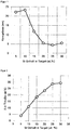
- the inventors have now completely surprisingly found that if such a method is operated with TiSi targets which contain a silicon content greater than or equal to 15 at%, it is possible to produce reproducible nanocrystalline layers with very good mechanical properties. It is particularly interesting that from a Si concentration in the target of 15at% the nanocrystals have an average grain size of less than 15 nm, as in FIG Figure 1 shown. That the concentration ratios in the target used for the coating are almost directly reflected in the coated layer is shown in Figure 2 shown. It should be noted at this point that as soon as a target with a certain Si concentration has been selected, the grain size can be finely adjusted via the nitrogen consumption, such as Figure 7 shows.
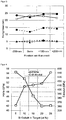
- the layers then have an increasing hardness and a decreasing modulus of elasticity as the silicon content increases, as in FIG Figure 4 shown. There, it is not the concentration ratios in the layers but the concentration ratios Ti / Si in the targets used for the production of the layers that are given.
- the Ti x Si 1-x N layer with at least 15at% Si content of the metallic components is not applied directly to the substrate to be coated but a TiAlN layer as an intermediate layer between the substrate and the layer according to the invention intended.
- This intermediate layer has the advantage, among other things, that it mediates between the less brittle substrate and the extremely hard Ti x Si 1-x N layer, which is loaded with very high internal stresses, with regard to the stress and / or pressure conditions. This means that there is much less flaking and the layer adhesion is improved accordingly.
- Figure 5 shows a series of such two - layer layers according to the invention, the different targets already discussed in accordance with the information in the figure being used for the coating of the Ti x Si 1-x layers.
- a target was used to produce the intermediate layer which comprises 40at% titanium and 60at% aluminum. It has been found that it is particularly advantageous if both layers TiAlN and TiSiN have a (200) texture.
- Such double layers with different Si contents were tested on tools.
- the machining tests were carried out under the following conditions: workpiece steel DIN 1.2344 hardened to 45HRC, tool diameter 10mm solid carbide cutter, cutting speed 220m / min, feed per tooth 0.1mm, axial infeed 10mm, radial infeed 0.5mm. It was measured through how many meters a corresponding tool can work without being damaged.
- Tool which is coated with a commercially available layer survives for a little more than 200m.
- Tools coated with the double layer described above survive for about the same time, with the outer layer only containing 5% silicon. In contrast, the tests showed that the tool survives more than 500m if the outer layer contains at least 15% silicon.
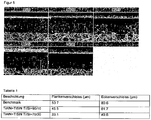
- Table 1 lists the wear values measured for the tools after a cutting path of 140 m. It can be clearly seen that the wear is lowest when coated with 30% silicon.
- a transition layer is provided between the TiAlN intermediate layer and the Ti x Si 1-x layer, which was produced by means of co-sputtering.
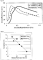
- cosputterning can be carried out reliably in such a way that, for example, the pulse lengths for the different targets are selected in such a way that the maxima of the reactive gas consumption curves are essentially superimposed depending on the pressure prevailing in the coating chamber. This is possible because the pulse duration has a direct influence on the position of the corresponding maxima. This is for an example in Figure 6 shown, where with 3 different pulse durations (0.05ms, 0.2ms and 2ms) it was sputtered in this way it is possible to operate both targets optimally with the same pressure and gas flow conditions prevailing in the chamber.
- the transition layer is implemented as a gradient layer which, with increasing distance from the substrate surface, has a decreasing proportion of TiAlN and an increasing proportion of Ti x Si 1-x N.
- the final Ti x Si 1-x N layer is not a pure Ti x Si 1-x N layer but rather still contains proportions of TiAlN.
- a first Ti x Si 1-x target and a second Ti z Si 1-z target are used for the coating, where 0 x 1 and 0 z 1 , but e.g. ⁇ x, ie first and second target differ in their composition and (x + z) / 2 ⁇ 0.85, so that layers with a Si concentration of ⁇ 15 at% can still be produced.
- both targets can then be operated using the co-sputtering method described above. This allows the Si concentration to be varied during the coating, ie to realize a Si concentration profile.
- the Ti x Si 1-x N layer with at least 15at% Si content of the metallic components is not applied directly to the substrate to be coated, but rather a Cr y Al 1- y N-layer provided as an intermediate layer.
- a chromium content of 40at% and an aluminum content of 60at% have proven to be advantageous.
- This intermediate layer has the advantage, among other things, that it mediates between the less brittle substrate and the extremely hard Ti x Si 1-x N layer, which is loaded with very high internal stresses, with regard to the stress and / or pressure conditions. This means that there is much less flaking and the layer adhesion is improved accordingly.
- x indicates the concentration of Ti expressed in at% and y indicates the concentration of Cr expressed in at% if only the metallic elements are taken into account.
- Such double layers with different Si contents were tested on tools. It was measured by how many meters a corresponding tool can work without being significantly damaged.
- the machining tests were carried out under the following conditions: workpiece steel DIN 1.2379 hardened to 69HRC, tool diameter 2mm solid carbide ball end mill, cutting speed 110m / min, feed per tooth 0.04mm, axial infeed 0.1mm, radial infeed 0.04mm.
- Tool coated with a commercially available layer survives for a little more than 60m.
- tools coated with the double layer described above, with the outer layer containing at least 10% silicon survive for more than 100m. It is interesting that the CrAlN layer should be kept relatively thin. This indicates that the CrAlN layer essentially takes on the function of an adhesive layer.
- a transition layer is provided between the CrAlN intermediate layer and the Ti x Si 1-x layer, which was produced by means of co-sputtering.
- cosputterning can be carried out reliably in such a way that, for example, the pulse lengths for the different targets are selected in such a way that the maxima of the reactive gas consumption curves are essentially superimposed depending on the pressure prevailing in the coating chamber. This is possible because the pulse duration has a direct influence on the position of the corresponding maxima. This is for an example in Figure 6 shown where 3 different pulse durations (0.05ms, 0.2ms and 2ms) were sputtered. In this way it is possible to operate both targets optimally with the same pressure and gas flow conditions prevailing in the chamber.
- the transition layer is implemented as a gradient layer which, with increasing distance from the substrate surface, has a decreasing proportion of CrAlN and an increasing proportion of Ti x Si 1-x N.
- the final Ti x Si 1-x N layer is not a pure Ti x Si 1-x N layer but rather still contains proportions of CrAlN.
- An intermediate layer which comprises TiAlN or CrAlN or TiAlN and CrAlN, is preferably provided between the Ti x Si 1-x N layer and the substrate body of the workpiece.
- the transition layer is produced by means of co-sputtering.
- the Ti x Si 1-x N layer obtained with the coating method according to the invention can be used according to the present invention Invention still contain proportions of TiAlN or CrAlN or TiAlN and CrAlN.
Landscapes
- Chemical & Material Sciences (AREA)
- Engineering & Computer Science (AREA)
- Mechanical Engineering (AREA)
- Chemical Kinetics & Catalysis (AREA)
- Materials Engineering (AREA)
- Metallurgy (AREA)
- Organic Chemistry (AREA)
- Physical Vapour Deposition (AREA)
- Cutting Tools, Boring Holders, And Turrets (AREA)
- Coating By Spraying Or Casting (AREA)
Priority Applications (1)
| Application Number | Priority Date | Filing Date | Title |
|---|---|---|---|
| PL14737148T PL3017079T5 (pl) | 2013-07-03 | 2014-07-01 | Sposób wytwarzania warstw tixsi1-xn |
Applications Claiming Priority (3)
| Application Number | Priority Date | Filing Date | Title |
|---|---|---|---|
| DE201310011071 DE102013011071A1 (de) | 2013-07-03 | 2013-07-03 | TixSi1-xN Schichten mit CryAl1-yN Haftschicht und ihre Herstellung |
| DE102013011073.4A DE102013011073A1 (de) | 2013-07-03 | 2013-07-03 | TlxSi1-xN Schichten und ihre Herstellung |
| PCT/EP2014/001792 WO2015000581A1 (de) | 2013-07-03 | 2014-07-01 | Tixsi1-xn schichten und ihre herstellung |
Publications (3)
| Publication Number | Publication Date |
|---|---|
| EP3017079A1 EP3017079A1 (de) | 2016-05-11 |
| EP3017079B1 EP3017079B1 (de) | 2017-04-12 |
| EP3017079B2 true EP3017079B2 (de) | 2020-09-09 |
Family
ID=51167846
Family Applications (1)
| Application Number | Title | Priority Date | Filing Date |
|---|---|---|---|
| EP14737148.8A Active EP3017079B2 (de) | 2013-07-03 | 2014-07-01 | Verfahren zur herstellung von tixsi1-xn schichten |
Country Status (18)
| Country | Link |
|---|---|
| US (1) | US9840768B2 (pl) |
| EP (1) | EP3017079B2 (pl) |
| JP (1) | JP6122975B2 (pl) |
| KR (2) | KR102178189B1 (pl) |
| CN (1) | CN105392911B (pl) |
| BR (1) | BR112015032169B1 (pl) |
| CA (1) | CA2916784C (pl) |
| ES (1) | ES2630316T5 (pl) |
| HK (1) | HK1219516A1 (pl) |
| IL (1) | IL243136A (pl) |
| MX (1) | MX361325B (pl) |
| MY (1) | MY187100A (pl) |
| PH (1) | PH12015502753A1 (pl) |
| PL (1) | PL3017079T5 (pl) |
| PT (1) | PT3017079T (pl) |
| RU (1) | RU2674179C2 (pl) |
| SG (1) | SG11201510417RA (pl) |
| WO (1) | WO2015000581A1 (pl) |
Families Citing this family (3)
| Publication number | Priority date | Publication date | Assignee | Title |
|---|---|---|---|---|
| KR102345375B1 (ko) * | 2016-03-30 | 2021-12-29 | 가부시키가이샤 몰디노 | 피복 절삭 공구 |
| KR102336097B1 (ko) * | 2017-09-27 | 2021-12-06 | 가부시키가이샤 몰디노 | 피복 절삭 공구 |
| CN115125486B (zh) * | 2022-07-27 | 2024-01-02 | 安徽工业大学 | 一种含有多层结构的高强韧纳米复合涂层及其制备方法 |
Citations (10)
| Publication number | Priority date | Publication date | Assignee | Title |
|---|---|---|---|---|
| EP1174528A2 (en) † | 2000-07-13 | 2002-01-23 | Hitachi Tool Engineering Ltd. | Multilayer-coated cutting tool |
| US20060147728A1 (en) † | 2004-05-03 | 2006-07-06 | Yaogen Shen | Multi-layered superhard nanocomposite coatings |
| WO2007129021A1 (en) † | 2006-05-02 | 2007-11-15 | Sheffield Hallam University | High power impulse magnetron sputtering vapour deposition |
| EP2072637A2 (en) † | 2007-12-21 | 2009-06-24 | Sandvik Intellectual Property AB | Coated cutting tool and a method of making a coated cutting tool |
| EP2336382A1 (en) † | 2009-12-04 | 2011-06-22 | Sandvik Intellectual Property AB | Multilayer coated cutting tool |
| WO2011149580A1 (en) † | 2010-05-28 | 2011-12-01 | Kennametal Inc. | Multilayer nitride hard coatings |
| WO2012143087A1 (de) † | 2011-04-20 | 2012-10-26 | Oerlikon Trading Ag, Trübbach | Hochleistungszerstäubungsquelle |
| WO2012143110A1 (en) † | 2011-04-20 | 2012-10-26 | Oerlikon Trading Ag, Trübbach | High power impulse magnetron sputtering method providing enhanced ionization of the sputtered particles and apparatus for its implementation |
| WO2013060415A1 (de) † | 2011-10-28 | 2013-05-02 | Oerlikon Trading AG,Trübbach | Verfahren zur bereitstellung sequenzieller leistungspulse |
| DE102012209293B3 (de) † | 2012-06-01 | 2013-06-20 | Helmholtz-Zentrum Dresden - Rossendorf E.V. | Sputterverfahren |
Family Cites Families (32)
| Publication number | Priority date | Publication date | Assignee | Title |
|---|---|---|---|---|
| JPH07197246A (ja) * | 1993-12-28 | 1995-08-01 | Mitsubishi Materials Corp | 成膜中にパーティクル発生の少ないスパッタリング用Tiシリサイド焼結ターゲット材 |
| JPH0867971A (ja) * | 1994-08-30 | 1996-03-12 | Mitsubishi Materials Corp | モザイク状Tiシリサイドターゲット材 |
| DE19625577A1 (de) | 1996-06-27 | 1998-01-02 | Vaw Motor Gmbh | Aluminium-Gußteil und Verfahren zu seiner Herstellung |
| JP3996809B2 (ja) | 2002-07-11 | 2007-10-24 | 住友電工ハードメタル株式会社 | 被覆切削工具 |
| US6906295B2 (en) * | 2003-02-20 | 2005-06-14 | National Material L.P. | Foodware with multilayer stick resistant ceramic coating and method of making |
| AU2003903853A0 (en) | 2003-07-25 | 2003-08-07 | Antoine Bittar | Barriers, materials and processes for solar selective surfaces |
| JP2005344148A (ja) * | 2004-06-01 | 2005-12-15 | Sumitomo Electric Ind Ltd | 耐摩耗性被膜およびこれを用いた表面被覆切削工具 |
| US7790003B2 (en) * | 2004-10-12 | 2010-09-07 | Southwest Research Institute | Method for magnetron sputter deposition |
| US7348074B2 (en) * | 2005-04-01 | 2008-03-25 | Oc Oerlikon Balzers Ag | Multilayer hard coating for tools |
| SE0500994L (sv) * | 2005-04-29 | 2006-10-30 | Seco Tools Ab | Tunt slitstarkt skikt |
| US8034459B2 (en) * | 2005-10-18 | 2011-10-11 | Southwest Research Institute | Erosion resistant coatings |
| CA2885593C (en) * | 2006-05-17 | 2018-03-06 | G & H Technologies Llc | Wear resistant coating |
| RU2327811C1 (ru) * | 2006-11-14 | 2008-06-27 | Государственное образовательное учреждение высшего профессионального образования "Ульяновский государственный технический университет" | Способ получения многослойного покрытия для режущего инструмента |
| SE0602814L (sv) * | 2006-12-27 | 2008-06-28 | Sandvik Intellectual Property | Skärverktyg med multiskiktbeläggning |
| EP2156912B1 (en) | 2007-05-30 | 2011-08-17 | Sumitomo Electric Hardmetal Corp. | Surface-coated cutting tool |
| JP5246165B2 (ja) * | 2007-10-12 | 2013-07-24 | 日立ツール株式会社 | 硬質皮膜被覆部材の製造方法 |
| PT2310549T (pt) | 2008-07-09 | 2018-02-08 | Oerlikon Surface Solutions Ltd Pfaeffikon | Sistema de revestimento, peça de trabalho revestida e método para produzir a mesma |
| EP2157205B1 (en) * | 2008-07-29 | 2011-11-30 | Sulzer Metaplas GmbH | A high-power pulsed magnetron sputtering process as well as a high-power electrical energy source |
| JP5156971B2 (ja) | 2009-03-17 | 2013-03-06 | Smc株式会社 | 溶損防止用被覆部材 |
| SE533883C2 (sv) | 2009-06-01 | 2011-02-22 | Seco Tools Ab | Nanolaminerat belagt skärverktyg |
| US8784977B2 (en) * | 2009-06-22 | 2014-07-22 | Tungaloy Corporation | Coated cubic boron nitride sintered body tool |
| JP5190971B2 (ja) * | 2009-12-16 | 2013-04-24 | 住友電気工業株式会社 | 被膜、切削工具および被膜の製造方法 |
| JP5896918B2 (ja) | 2010-01-11 | 2016-03-30 | イスカーリミテッド | 被覆切削工具 |
| JP2011167793A (ja) * | 2010-02-18 | 2011-09-01 | Mitsubishi Materials Corp | 表面被覆切削工具 |
| RU2428509C1 (ru) * | 2010-04-13 | 2011-09-10 | Государственное образовательное учреждение высшего профессионального образования "Ульяновский государственный технический университет" | Способ получения многослойного покрытия для режущего инструмента |
| RU2419680C1 (ru) * | 2010-04-20 | 2011-05-27 | Государственное образовательное учреждение высшего профессионального образования "Ульяновский государственный технический университет" | Способ получения многослойного покрытия для режущего инструмента |
| BR112012027155A2 (pt) * | 2010-04-23 | 2019-09-24 | Seco Tools Ab | revestimento por deposição física de vapor para usinagem de metal |
| JP5392408B2 (ja) * | 2010-07-06 | 2014-01-22 | 株式会社タンガロイ | 被覆cBN焼結体工具 |
| DE102010034321B4 (de) | 2010-08-09 | 2017-04-06 | Technische Universität Dresden | Verfahren zur Herstellung einer Hartstoffbeschichtung auf metallischen, keramischen oder hartmetallischen Bauteilen sowie eine mit dem Verfahren hergestellte Hartstoffbeschichtung |
| WO2012070290A1 (ja) | 2010-11-26 | 2012-05-31 | 住友電工ハードメタル株式会社 | 表面被覆焼結体 |
| DE102011053372A1 (de) | 2011-09-07 | 2013-03-07 | Walter Ag | Werkzeug mit chromhaltiger Funktionsschicht |
| CN104272429B (zh) | 2011-12-05 | 2016-08-24 | 欧瑞康表面解决方案股份公司,普费菲孔 | 用于反应溅射的方法 |
-
2014
- 2014-07-01 SG SG11201510417RA patent/SG11201510417RA/en unknown
- 2014-07-01 CA CA2916784A patent/CA2916784C/en not_active Expired - Fee Related
- 2014-07-01 EP EP14737148.8A patent/EP3017079B2/de active Active
- 2014-07-01 KR KR1020177026135A patent/KR102178189B1/ko active IP Right Grant
- 2014-07-01 MX MX2015017033A patent/MX361325B/es active IP Right Grant
- 2014-07-01 ES ES14737148T patent/ES2630316T5/es active Active
- 2014-07-01 RU RU2016102845A patent/RU2674179C2/ru active
- 2014-07-01 MY MYPI2015704719A patent/MY187100A/en unknown
- 2014-07-01 JP JP2015563197A patent/JP6122975B2/ja active Active
- 2014-07-01 PT PT147371488T patent/PT3017079T/pt unknown
- 2014-07-01 CN CN201480037761.2A patent/CN105392911B/zh active Active
- 2014-07-01 BR BR112015032169-0A patent/BR112015032169B1/pt active IP Right Grant
- 2014-07-01 KR KR1020167002703A patent/KR101891900B1/ko active IP Right Grant
- 2014-07-01 WO PCT/EP2014/001792 patent/WO2015000581A1/de active Application Filing
- 2014-07-01 PL PL14737148T patent/PL3017079T5/pl unknown
- 2014-07-01 US US14/902,826 patent/US9840768B2/en active Active
-
2015
- 2015-12-09 PH PH12015502753A patent/PH12015502753A1/en unknown
- 2015-12-15 IL IL243136A patent/IL243136A/en active IP Right Grant
-
2016
- 2016-06-29 HK HK16107568.9A patent/HK1219516A1/zh unknown
Patent Citations (11)
| Publication number | Priority date | Publication date | Assignee | Title |
|---|---|---|---|---|
| EP1174528A2 (en) † | 2000-07-13 | 2002-01-23 | Hitachi Tool Engineering Ltd. | Multilayer-coated cutting tool |
| US20060147728A1 (en) † | 2004-05-03 | 2006-07-06 | Yaogen Shen | Multi-layered superhard nanocomposite coatings |
| WO2007129021A1 (en) † | 2006-05-02 | 2007-11-15 | Sheffield Hallam University | High power impulse magnetron sputtering vapour deposition |
| EP2072637A2 (en) † | 2007-12-21 | 2009-06-24 | Sandvik Intellectual Property AB | Coated cutting tool and a method of making a coated cutting tool |
| EP2336382A1 (en) † | 2009-12-04 | 2011-06-22 | Sandvik Intellectual Property AB | Multilayer coated cutting tool |
| WO2011149580A1 (en) † | 2010-05-28 | 2011-12-01 | Kennametal Inc. | Multilayer nitride hard coatings |
| WO2012143087A1 (de) † | 2011-04-20 | 2012-10-26 | Oerlikon Trading Ag, Trübbach | Hochleistungszerstäubungsquelle |
| WO2012143110A1 (en) † | 2011-04-20 | 2012-10-26 | Oerlikon Trading Ag, Trübbach | High power impulse magnetron sputtering method providing enhanced ionization of the sputtered particles and apparatus for its implementation |
| WO2013060415A1 (de) † | 2011-10-28 | 2013-05-02 | Oerlikon Trading AG,Trübbach | Verfahren zur bereitstellung sequenzieller leistungspulse |
| DE102011117177A1 (de) † | 2011-10-28 | 2013-05-02 | Oerlikon Trading Ag, Trübbach | Verfahren zur Bereitstellung sequenzieller Leistungspulse |
| DE102012209293B3 (de) † | 2012-06-01 | 2013-06-20 | Helmholtz-Zentrum Dresden - Rossendorf E.V. | Sputterverfahren |
Non-Patent Citations (7)
| Title |
|---|
| BOBZIN K. ET AL: "Advantages of nanocomposite coatings deposited by high power pulse magnetron sputtering technology", JOURNAL OF MATERIALS PROCESSING TECHNOLOGY , vol. 209, no. 1, 1 January 2009 (2009-01-01), pages 165 - 170, DOI: 10.1016/j.jmatprotec.2008.01.035 † |
| BOBZIN K. ET AL: "Properties of (Ti,Al,Si)N Coatings for High Demanding Metal Cutting Applications Deposited by HPPMS in an Industrial Coating Unit", PLASMA PROCESS. POLYM. , vol. 6, 1 January 2009 (2009-01-01), pages S124 - S128, DOI: 10.1002/ppap.200930408 † |
| EHIASARIAN A.P. ET AL: "Influence of high power impulse magnetron sputtering plasma ionization on the microstructure of TiN thin films", JOURNAL OF APPLIED PHYSICS, vol. 109, 1 January 2011 (2011-01-01), pages 104314-1 - 104314-15, DOI: 10.1063/1.3579443 † |
| EHIASARIAN A.P.: "High-power impulse magnetron sputtering and its applications", PURE APPL. CHEM., vol. 82, no. 6, 1 January 2010 (2010-01-01), pages 1247 - 1258, DOI: 10.1351/PAC-CON-09-10-43 † |
| SHTANSKY D.V. ET AL: "Comparative investigation of Ti–Si–N films magnetron sputtered using Ti5Si3+Ti and Ti5Si3+TiN targets", SURFACE AND COATINGS TECHNOLOGY, vol. 182, no. 2-3, 22 April 2004 (2004-04-22), pages 204 - 214, DOI: 10.1016/j.surfcoat.2003.08.052 † |
| VAZ F ET AL: "Structural analysis of Ti1-xSixNy nanocomposite films prepared by reactive magnetron sputtering", SURFACE AND COATINGS TECHNOLOGY, ELSEVIER, AMSTERDAM, NL, vol. 120-121, 1 November 1999 (1999-11-01), pages 166 - 172, ISSN: 0257-8972, [retrieved on 19991101] † |
| Wikipedia Article on High-power impulse Magnetron sputtering (revision of page edited 20-02-2013) † |
Also Published As
Similar Documents
| Publication | Publication Date | Title |
|---|---|---|
| EP3215651B1 (de) | Pvd verfahren zur herstellung eines schneidwerkzeugs mit mehrlagiger beschichtung | |
| DE102005063536B4 (de) | Hartstoff - Schichtsystem | |
| EP0798399B1 (de) | Verfahren zum Beschichten von metallischen und keramischen substraten | |
| DE19517120C2 (de) | Beschichtetes Teil mit ausgezeichneter Härte und Haftung, seine Verwendung und Verfahren zur Herstellung | |
| EP2893053B1 (de) | Verfahren zur herstellung einer metallborocarbidschicht auf einem substrat | |
| EP3056587B1 (de) | VHM-Schaftfräser mit TiAlN-ZrN-Beschichtung | |
| WO2009127344A1 (de) | Beschichtungsverfahren, werkstück oder werkzeug und dessen verwendung | |
| DE3825399C2 (de) | PVD- oder Plasma- CVD-Beschichtung und Verfahren zu ihrer Herstellung | |
| EP2653583A1 (de) | Beschichtungsverfahren zur Abscheidung eines Schichtsystems auf einem Substrat, sowie Substrat mit einem Schichtsystem | |
| EP2912207A1 (de) | Bauteil mit einer beschichtung und verfahren zu seiner herstellung | |
| DE102013011075A1 (de) | TiB2 Schichten und ihre Herstellung | |
| EP3017079B2 (de) | Verfahren zur herstellung von tixsi1-xn schichten | |
| DE102010034321B4 (de) | Verfahren zur Herstellung einer Hartstoffbeschichtung auf metallischen, keramischen oder hartmetallischen Bauteilen sowie eine mit dem Verfahren hergestellte Hartstoffbeschichtung | |
| DE102011117994A1 (de) | HIPIMS-Schichten | |
| EP2872666A1 (de) | Hochleistungsimpulsbeschichtungsverfahren | |
| EP2286643B1 (de) | Vorrichtung und verfahren zum hochleistungs-puls-gasfluss-sputtern | |
| DE102013011073A1 (de) | TlxSi1-xN Schichten und ihre Herstellung | |
| EP2989654B1 (de) | Lichtbogenverdampfungs-beschichtungsquelle mit permanentmagnet | |
| EP3445890B1 (de) | Ticn mit reduzierten wachstumsdefekten mittels hipims | |
| EP3019640B1 (de) | Target zur reaktiven sputter-abscheidung elektrisch-isolierender schichten | |
| DE102013011071A1 (de) | TixSi1-xN Schichten mit CryAl1-yN Haftschicht und ihre Herstellung | |
| WO2019223959A1 (de) | Magnetronsputtervorrichtung | |
| DE102011108088B4 (de) | Werkzeug mit einer nitridischen Hartstoffschicht sowie Verfahren zu dessen Herstellung | |
| Kurapov et al. | Ti x Si 1-x N layers and their production | |
| WO2024068155A1 (de) | Verfahren zur beschichtung eines werkzeugteils eines spanabhebenden werkzeugs |
Legal Events
| Date | Code | Title | Description |
|---|---|---|---|
| PUAI | Public reference made under article 153(3) epc to a published international application that has entered the european phase |
Free format text: ORIGINAL CODE: 0009012 |
|
| 17P | Request for examination filed |
Effective date: 20160129 |
|
| AK | Designated contracting states |
Kind code of ref document: A1 Designated state(s): AL AT BE BG CH CY CZ DE DK EE ES FI FR GB GR HR HU IE IS IT LI LT LU LV MC MK MT NL NO PL PT RO RS SE SI SK SM TR |
|
| AX | Request for extension of the european patent |
Extension state: BA ME |
|
| RIN1 | Information on inventor provided before grant (corrected) |
Inventor name: KURAPOV, DENIS Inventor name: KRASSNITZER, SIEGFRIED |
|
| GRAP | Despatch of communication of intention to grant a patent |
Free format text: ORIGINAL CODE: EPIDOSNIGR1 |
|
| INTG | Intention to grant announced |
Effective date: 20160623 |
|
| GRAJ | Information related to disapproval of communication of intention to grant by the applicant or resumption of examination proceedings by the epo deleted |
Free format text: ORIGINAL CODE: EPIDOSDIGR1 |
|
| DAX | Request for extension of the european patent (deleted) | ||
| RAP1 | Party data changed (applicant data changed or rights of an application transferred) |
Owner name: OERLIKON SURFACE SOLUTIONS AG, PFAEFFIKON |
|
| GRAP | Despatch of communication of intention to grant a patent |
Free format text: ORIGINAL CODE: EPIDOSNIGR1 |
|
| INTG | Intention to grant announced |
Effective date: 20161019 |
|
| GRAS | Grant fee paid |
Free format text: ORIGINAL CODE: EPIDOSNIGR3 |
|
| STAA | Information on the status of an ep patent application or granted ep patent |
Free format text: STATUS: GRANT OF PATENT IS INTENDED |
|
| GRAA | (expected) grant |
Free format text: ORIGINAL CODE: 0009210 |
|
| STAA | Information on the status of an ep patent application or granted ep patent |
Free format text: STATUS: THE PATENT HAS BEEN GRANTED |
|
| AK | Designated contracting states |
Kind code of ref document: B1 Designated state(s): AL AT BE BG CH CY CZ DE DK EE ES FI FR GB GR HR HU IE IS IT LI LT LU LV MC MK MT NL NO PL PT RO RS SE SI SK SM TR |
|
| REG | Reference to a national code |
Ref country code: GB Ref legal event code: FG4D Free format text: NOT ENGLISH |
|
| REG | Reference to a national code |
Ref country code: CH Ref legal event code: EP |
|
| REG | Reference to a national code |
Ref country code: IE Ref legal event code: FG4D Free format text: LANGUAGE OF EP DOCUMENT: GERMAN |
|
| REG | Reference to a national code |
Ref country code: AT Ref legal event code: REF Ref document number: 883965 Country of ref document: AT Kind code of ref document: T Effective date: 20170515 |
|
| REG | Reference to a national code |
Ref country code: DE Ref legal event code: R096 Ref document number: 502014003430 Country of ref document: DE |
|
| REG | Reference to a national code |
Ref country code: RO Ref legal event code: EPE |
|
| REG | Reference to a national code |
Ref country code: NL Ref legal event code: FP Ref country code: PT Ref legal event code: SC4A Ref document number: 3017079 Country of ref document: PT Date of ref document: 20170719 Kind code of ref document: T Free format text: AVAILABILITY OF NATIONAL TRANSLATION Effective date: 20170712 |
|
| REG | Reference to a national code |
Ref country code: SE Ref legal event code: TRGR |
|
| REG | Reference to a national code |
Ref country code: FR Ref legal event code: PLFP Year of fee payment: 4 |
|
| REG | Reference to a national code |
Ref country code: ES Ref legal event code: FG2A Ref document number: 2630316 Country of ref document: ES Kind code of ref document: T3 Effective date: 20170821 |
|
| REG | Reference to a national code |
Ref country code: LT Ref legal event code: MG4D |
|
| PG25 | Lapsed in a contracting state [announced via postgrant information from national office to epo] |
Ref country code: LT Free format text: LAPSE BECAUSE OF FAILURE TO SUBMIT A TRANSLATION OF THE DESCRIPTION OR TO PAY THE FEE WITHIN THE PRESCRIBED TIME-LIMIT Effective date: 20170412 Ref country code: HR Free format text: LAPSE BECAUSE OF FAILURE TO SUBMIT A TRANSLATION OF THE DESCRIPTION OR TO PAY THE FEE WITHIN THE PRESCRIBED TIME-LIMIT Effective date: 20170412 Ref country code: NO Free format text: LAPSE BECAUSE OF FAILURE TO SUBMIT A TRANSLATION OF THE DESCRIPTION OR TO PAY THE FEE WITHIN THE PRESCRIBED TIME-LIMIT Effective date: 20170712 Ref country code: GR Free format text: LAPSE BECAUSE OF FAILURE TO SUBMIT A TRANSLATION OF THE DESCRIPTION OR TO PAY THE FEE WITHIN THE PRESCRIBED TIME-LIMIT Effective date: 20170713 |
|
| PG25 | Lapsed in a contracting state [announced via postgrant information from national office to epo] |
Ref country code: BG Free format text: LAPSE BECAUSE OF FAILURE TO SUBMIT A TRANSLATION OF THE DESCRIPTION OR TO PAY THE FEE WITHIN THE PRESCRIBED TIME-LIMIT Effective date: 20170712 Ref country code: IS Free format text: LAPSE BECAUSE OF FAILURE TO SUBMIT A TRANSLATION OF THE DESCRIPTION OR TO PAY THE FEE WITHIN THE PRESCRIBED TIME-LIMIT Effective date: 20170812 Ref country code: LV Free format text: LAPSE BECAUSE OF FAILURE TO SUBMIT A TRANSLATION OF THE DESCRIPTION OR TO PAY THE FEE WITHIN THE PRESCRIBED TIME-LIMIT Effective date: 20170412 Ref country code: RS Free format text: LAPSE BECAUSE OF FAILURE TO SUBMIT A TRANSLATION OF THE DESCRIPTION OR TO PAY THE FEE WITHIN THE PRESCRIBED TIME-LIMIT Effective date: 20170412 |
|
| REG | Reference to a national code |
Ref country code: SK Ref legal event code: T3 Ref document number: E 24736 Country of ref document: SK |
|
| REG | Reference to a national code |
Ref country code: DE Ref legal event code: R026 Ref document number: 502014003430 Country of ref document: DE |
|
| PLBI | Opposition filed |
Free format text: ORIGINAL CODE: 0009260 |
|
| REG | Reference to a national code |
Ref country code: HU Ref legal event code: AG4A Ref document number: E033853 Country of ref document: HU |
|
| PG25 | Lapsed in a contracting state [announced via postgrant information from national office to epo] |
Ref country code: EE Free format text: LAPSE BECAUSE OF FAILURE TO SUBMIT A TRANSLATION OF THE DESCRIPTION OR TO PAY THE FEE WITHIN THE PRESCRIBED TIME-LIMIT Effective date: 20170412 Ref country code: DK Free format text: LAPSE BECAUSE OF FAILURE TO SUBMIT A TRANSLATION OF THE DESCRIPTION OR TO PAY THE FEE WITHIN THE PRESCRIBED TIME-LIMIT Effective date: 20170412 |
|
| PLAX | Notice of opposition and request to file observation + time limit sent |
Free format text: ORIGINAL CODE: EPIDOSNOBS2 |
|
| 26 | Opposition filed |
Opponent name: IHI IONBOND AG Effective date: 20180112 |
|
| PG25 | Lapsed in a contracting state [announced via postgrant information from national office to epo] |
Ref country code: SM Free format text: LAPSE BECAUSE OF FAILURE TO SUBMIT A TRANSLATION OF THE DESCRIPTION OR TO PAY THE FEE WITHIN THE PRESCRIBED TIME-LIMIT Effective date: 20170412 |
|
| REG | Reference to a national code |
Ref country code: IE Ref legal event code: MM4A |
|
| PG25 | Lapsed in a contracting state [announced via postgrant information from national office to epo] |
Ref country code: IE Free format text: LAPSE BECAUSE OF NON-PAYMENT OF DUE FEES Effective date: 20170701 |
|
| PG25 | Lapsed in a contracting state [announced via postgrant information from national office to epo] |
Ref country code: SI Free format text: LAPSE BECAUSE OF FAILURE TO SUBMIT A TRANSLATION OF THE DESCRIPTION OR TO PAY THE FEE WITHIN THE PRESCRIBED TIME-LIMIT Effective date: 20170412 |
|
| PLAF | Information modified related to communication of a notice of opposition and request to file observations + time limit |
Free format text: ORIGINAL CODE: EPIDOSCOBS2 |
|
| PLBB | Reply of patent proprietor to notice(s) of opposition received |
Free format text: ORIGINAL CODE: EPIDOSNOBS3 |
|
| REG | Reference to a national code |
Ref country code: FR Ref legal event code: PLFP Year of fee payment: 5 |
|
| PG25 | Lapsed in a contracting state [announced via postgrant information from national office to epo] |
Ref country code: MT Free format text: LAPSE BECAUSE OF FAILURE TO SUBMIT A TRANSLATION OF THE DESCRIPTION OR TO PAY THE FEE WITHIN THE PRESCRIBED TIME-LIMIT Effective date: 20170412 |
|
| PG25 | Lapsed in a contracting state [announced via postgrant information from national office to epo] |
Ref country code: MC Free format text: LAPSE BECAUSE OF FAILURE TO SUBMIT A TRANSLATION OF THE DESCRIPTION OR TO PAY THE FEE WITHIN THE PRESCRIBED TIME-LIMIT Effective date: 20170412 |
|
| PG25 | Lapsed in a contracting state [announced via postgrant information from national office to epo] |
Ref country code: CY Free format text: LAPSE BECAUSE OF FAILURE TO SUBMIT A TRANSLATION OF THE DESCRIPTION OR TO PAY THE FEE WITHIN THE PRESCRIBED TIME-LIMIT Effective date: 20170412 |
|
| PG25 | Lapsed in a contracting state [announced via postgrant information from national office to epo] |
Ref country code: MK Free format text: LAPSE BECAUSE OF FAILURE TO SUBMIT A TRANSLATION OF THE DESCRIPTION OR TO PAY THE FEE WITHIN THE PRESCRIBED TIME-LIMIT Effective date: 20170412 |
|
| APBM | Appeal reference recorded |
Free format text: ORIGINAL CODE: EPIDOSNREFNO |
|
| APBP | Date of receipt of notice of appeal recorded |
Free format text: ORIGINAL CODE: EPIDOSNNOA2O |
|
| APAH | Appeal reference modified |
Free format text: ORIGINAL CODE: EPIDOSCREFNO |
|
| APBU | Appeal procedure closed |
Free format text: ORIGINAL CODE: EPIDOSNNOA9O |
|
| PG25 | Lapsed in a contracting state [announced via postgrant information from national office to epo] |
Ref country code: AL Free format text: LAPSE BECAUSE OF FAILURE TO SUBMIT A TRANSLATION OF THE DESCRIPTION OR TO PAY THE FEE WITHIN THE PRESCRIBED TIME-LIMIT Effective date: 20170412 |
|
| PGFP | Annual fee paid to national office [announced via postgrant information from national office to epo] |
Ref country code: PT Payment date: 20200629 Year of fee payment: 7 Ref country code: TR Payment date: 20200630 Year of fee payment: 7 |
|
| PUAH | Patent maintained in amended form |
Free format text: ORIGINAL CODE: 0009272 |
|
| STAA | Information on the status of an ep patent application or granted ep patent |
Free format text: STATUS: PATENT MAINTAINED AS AMENDED |
|
| REG | Reference to a national code |
Ref country code: CH Ref legal event code: AELC |
|
| PGFP | Annual fee paid to national office [announced via postgrant information from national office to epo] |
Ref country code: SK Payment date: 20200630 Year of fee payment: 7 |
|
| 27A | Patent maintained in amended form |
Effective date: 20200909 |
|
| AK | Designated contracting states |
Kind code of ref document: B2 Designated state(s): AL AT BE BG CH CY CZ DE DK EE ES FI FR GB GR HR HU IE IS IT LI LT LU LV MC MK MT NL NO PL PT RO RS SE SI SK SM TR |
|
| REG | Reference to a national code |
Ref country code: DE Ref legal event code: R102 Ref document number: 502014003430 Country of ref document: DE |
|
| PGFP | Annual fee paid to national office [announced via postgrant information from national office to epo] |
Ref country code: RO Payment date: 20200701 Year of fee payment: 7 Ref country code: ES Payment date: 20200807 Year of fee payment: 7 Ref country code: FI Payment date: 20200721 Year of fee payment: 7 |
|
| REG | Reference to a national code |
Ref country code: CH Ref legal event code: NV Representative=s name: VALIPAT S.A. C/O BOVARD SA NEUCHATEL, CH |
|
| REG | Reference to a national code |
Ref country code: NL Ref legal event code: FP |
|
| PG25 | Lapsed in a contracting state [announced via postgrant information from national office to epo] |
Ref country code: SK Free format text: LAPSE BECAUSE OF FAILURE TO SUBMIT A TRANSLATION OF THE DESCRIPTION OR TO PAY THE FEE WITHIN THE PRESCRIBED TIME-LIMIT Effective date: 20200909 |
|
| PG25 | Lapsed in a contracting state [announced via postgrant information from national office to epo] |
Ref country code: PT Free format text: LAPSE BECAUSE OF FAILURE TO SUBMIT A TRANSLATION OF THE DESCRIPTION OR TO PAY THE FEE WITHIN THE PRESCRIBED TIME-LIMIT Effective date: 20210121 |
|
| REG | Reference to a national code |
Ref country code: ES Ref legal event code: DC2A Ref document number: 2630316 Country of ref document: ES Kind code of ref document: T5 Effective date: 20210618 |
|
| REG | Reference to a national code |
Ref country code: FI Ref legal event code: MAE |
|
| PG25 | Lapsed in a contracting state [announced via postgrant information from national office to epo] |
Ref country code: FI Free format text: LAPSE BECAUSE OF NON-PAYMENT OF DUE FEES Effective date: 20210701 |
|
| PG25 | Lapsed in a contracting state [announced via postgrant information from national office to epo] |
Ref country code: RO Free format text: LAPSE BECAUSE OF NON-PAYMENT OF DUE FEES Effective date: 20210701 |
|
| REG | Reference to a national code |
Ref country code: ES Ref legal event code: FD2A Effective date: 20220905 |
|
| PG25 | Lapsed in a contracting state [announced via postgrant information from national office to epo] |
Ref country code: ES Free format text: LAPSE BECAUSE OF NON-PAYMENT OF DUE FEES Effective date: 20210702 |
|
| PGFP | Annual fee paid to national office [announced via postgrant information from national office to epo] |
Ref country code: PL Payment date: 20230630 Year of fee payment: 10 Ref country code: NL Payment date: 20230726 Year of fee payment: 10 Ref country code: LU Payment date: 20230726 Year of fee payment: 10 |
|
| PGFP | Annual fee paid to national office [announced via postgrant information from national office to epo] |
Ref country code: IT Payment date: 20230721 Year of fee payment: 10 Ref country code: GB Payment date: 20230725 Year of fee payment: 10 Ref country code: CZ Payment date: 20230630 Year of fee payment: 10 Ref country code: CH Payment date: 20230801 Year of fee payment: 10 Ref country code: AT Payment date: 20230718 Year of fee payment: 10 |
|
| PGFP | Annual fee paid to national office [announced via postgrant information from national office to epo] |
Ref country code: SE Payment date: 20230726 Year of fee payment: 10 Ref country code: HU Payment date: 20230629 Year of fee payment: 10 Ref country code: FR Payment date: 20230725 Year of fee payment: 10 Ref country code: DE Payment date: 20230726 Year of fee payment: 10 Ref country code: BE Payment date: 20230726 Year of fee payment: 10 |