EP3004903B1 - Schaltung und layouttechniken für bereichs- und leistungsoptimierung für flop-tray - Google Patents
Schaltung und layouttechniken für bereichs- und leistungsoptimierung für flop-tray Download PDFInfo
- Publication number
- EP3004903B1 EP3004903B1 EP14733455.1A EP14733455A EP3004903B1 EP 3004903 B1 EP3004903 B1 EP 3004903B1 EP 14733455 A EP14733455 A EP 14733455A EP 3004903 B1 EP3004903 B1 EP 3004903B1
- Authority
- EP
- European Patent Office
- Prior art keywords
- scan
- flop
- flip
- input
- signal
- Prior art date
- Legal status (The legal status is an assumption and is not a legal conclusion. Google has not performed a legal analysis and makes no representation as to the accuracy of the status listed.)
- Active
Links
Images


Classifications
-
- G—PHYSICS
- G01—MEASURING; TESTING
- G01R—MEASURING ELECTRIC VARIABLES; MEASURING MAGNETIC VARIABLES
- G01R31/00—Arrangements for testing electric properties; Arrangements for locating electric faults; Arrangements for electrical testing characterised by what is being tested not provided for elsewhere
- G01R31/28—Testing of electronic circuits, e.g. by signal tracer
- G01R31/317—Testing of digital circuits
- G01R31/3177—Testing of logic operation, e.g. by logic analysers
-
- G—PHYSICS
- G01—MEASURING; TESTING
- G01R—MEASURING ELECTRIC VARIABLES; MEASURING MAGNETIC VARIABLES
- G01R31/00—Arrangements for testing electric properties; Arrangements for locating electric faults; Arrangements for electrical testing characterised by what is being tested not provided for elsewhere
- G01R31/28—Testing of electronic circuits, e.g. by signal tracer
- G01R31/317—Testing of digital circuits
- G01R31/3181—Functional testing
- G01R31/3185—Reconfiguring for testing, e.g. LSSD, partitioning
- G01R31/318533—Reconfiguring for testing, e.g. LSSD, partitioning using scanning techniques, e.g. LSSD, Boundary Scan, JTAG
- G01R31/318541—Scan latches or cell details
Definitions
- aspects of the present disclosure relate generally to scannable flop trays, and more particularly, to reducing the scan overhead of a scannable flop tray.
- Flip-flops may be used in a system to capture (latch) data values from one or more data signals for processing by various components of the system.
- the system may include scan circuitry to verify that the flip-flops are functioning correctly during testing. To do this, the scan circuitry receives a scan signal having a known test pattern, and scans the scan signal through the flip-flops. After the scan signal has been scanned through the flip-flops, the output scan signal is compared with an expected output scan signal to determine whether the flip-flops are functioning correctly. The expected output scan signal may be based on the known test pattern of the input scan signal and the expected functionality of the flip-flops.
- the scan circuitry adds overhead to the system due to the chip area and/power consumed by the scan circuitry.
- the area optimized flip-flop also provides a bypass mode:
- the bypass mode allows the area optimized flip-flops to act like a buffer. This allows the area optimized flip-flop to provide the basic functionality of a flip-flop during standard operation, but also allows the area optimized flip-flop to act like a buffer when desirable, such as during modes of testing of the design.
- the area optimized flip-flop provides most of the functionality of a typical flip-flop, while reducing the total area and power consumption of the design.
- a scan flip-flop circuit including a data input, a scan input, a data output, a flip-flop, a multiplexer and a delay element.
- the multiplexer allows selection of either the scan input or the data input for presentation at the input of the flip-flop.
- the flip-flop provides an output signal at the output of the scan flip-flop.
- the delay element is in a signal path between the scan input and the input of the flip-flop, and provides a signal propagation delay between the scan input and the input of the flip-flop. The delay between the scan input and the input of the flip-flop is substantially larger than the signal propagation delay between the data input and the input of the flip-flop.
- the delay in the scan path reduces the need for external buffers to avoid hold-time violations during scan testing of integrated circuits.
- a self-resetting dynamic circuit also known as a fireball circuit, contains a scan circuit and at least one Set Dominant Latches ("SDL") where each SDL includes a keeper node.
- SDL Set Dominant Latches
- a scan circuit and a method for scanning a flop tray as set forth in the independent claims, is provided.
- Embodiments of the invention are claimed in the dependent claims.
- the following presents a simplified summary of one or more embodiments in order to provide a basic understanding of such embodiments. This summary is not an extensive overview of all contemplated embodiments, and is intended to neither identify key or critical elements of all embodiments nor delineate the scope of any or all embodiments. Its sole purpose is to present some concepts of one or more embodiments in a simplified form as a prelude to the more detailed description that is presented later.
- a scan circuit for a flop tray comprises a tri-state circuit configured to invert an input data signal and output the inverted data signal to an input of a flip-flop of the flop tray in a normal mode, and to block the data signal from the input of the flip-flop in a scan mode.
- the scan circuit also comprises a pass gate configured to pass a scan signal to the input of the flip-flop in the scan mode, and to block the scan signal from the input of the flip-flop in the normal mode.
- a second aspect relates to a scan circuit for a flop tray.
- the scan circuit comprises a first tri-state circuit configured to invert a first data signal and output the inverted first data signal to an input of a first flip-flop of the flop tray in a normal mode, and to block the first data signal from the input of the first flip-flop in a scan mode.
- the scan circuit also comprises a first pass gate configured to pass a scan signal to the input of the first flip-flop in the scan mode, and to block the scan signal from the input of the first flip-flop in the normal mode.
- the scan circuit also comprises a second tri-state circuit configured to invert a second data signal and output the inverted second data signal to an input of a second flip-flop of the flop tray in the normal mode, and to block the second data signal from the input of the second flip-flop in the scan mode.
- the circuit further comprises a second pass gate configured to pass the scan signal from an output of the first flip-flop to the input of the second flip-flop in the scan mode, and to block the scan signal from the output of the first flip-flop from the input of the second flip-flop in the normal mode.
- a third aspect relates to a method for scanning a flop tray.
- the method comprises inverting an input data signal and outputting the inverted data signal to an input of a flip-flop of the flop tray in a normal mode using a tri-state circuit, and blocking the data signal from the input of the flip-flop in a scan mode using the tri-state circuit.
- the method also comprises passing a scan signal to the input of the flip-flop in the scan mode using a pass gate, and blocking the scan signal from the input of the flip-flop in the normal mode using the pass gate.
- a fourth aspect relates to an apparatus for scanning a flop tray.
- the apparatus comprises means for inverting an input data signal and outputting the inverted data signal to an input of a flip-flop of the flop tray in a normal mode, and means for blocking the data signal from the input of the flip-flop in a scan mode.
- the apparatus also comprises means for passing a scan signal to the input of the flip-flop in the scan mode, and means for blocking the scan signal from the input of the flip-flop in the normal mode.
- the one or more embodiments comprise the features hereinafter fully described and particularly pointed out in the claims.
- the following description and the annexed drawings set forth in detail certain illustrative aspects of the one or more embodiments. These aspects are indicative, however, of but a few of the various ways in which the principles of various embodiments may be employed and the described embodiments are intended to include all such aspects and their equivalents.
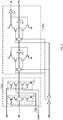
- FIG. 1 shows an example of a scannable flop tray 100.
- the flop tray 100 can operate in a normal mode or a scan mode.
- the flop tray 100 is operated in the scan mode during testing to test the correct functionality of the flop tray 100.
- the flop tray 100 comprises a first D flip-flop 120a, a second D flip-flop 120b, a third D flip-flop 120c, a fourth D flip-flop 120d, and scan circuitry 115.
- the scan circuitry 115 is used to operate the flop tray 100 in the scan mode during testing, as discussed further below.
- the scan circuitry 115 comprises a first scan multiplexer 110a, a second scan multiplexer 110b, a third scan multiplexer 110c, a fourth scan multiplexer 110d, and an inverted-polarity NAND gate 130.
- Each scan multiplexer 110a-110d is coupled to a respective one of the D flip-flops 120a-120d, in which the first scan multiplexer 110a is coupled to the input of the first D flip-flop 120a, the second scan multiplexer 110b is coupled to the input of the second D flip-flop 120b, and so forth.
- the scan circuitry 115 constitutes the scan overhead of the flop tray 100.
- the flop tray 100 receives a plurality of data signals d0-d3 in parallel.
- Each scan multiplexer 110a-110d receives one of the parallel data signals d0-d3 at a data input (labeled "0" in FIG. 1 ), and passes the respective data signal d0-d3 to the input of the respective D flip-flop 120a-120d.
- Each D flip-flop 120a-120d captures a data value (e.g., a bit) from the respective data signal d0-d3 on a rising or falling edge of a clock signal clk, and outputs the captured data value q0-q3.
- the flop tray 100 captures a plurality of data values (e.g., bits) in parallel from the data signals d0-d3 on a rising or falling edge of the clock signal clk, and outputs the captured data values q0-q3 in parallel.
- FIG. 1 shows an example of a four-bit flop tray comprising four flip-flops. However, it is to be appreciated that the present disclosure is not limited to this example, and can be applied to a flop tray comprising any number of flip-flops.
- the first scan multiplexer 110a couples a scan input of the flop tray 100 (labeled "sin" in FIG. 1 ) to the input of the first flip-flop 120a.
- Each of the remaining scan multiplexers 110b-110d couples the nq output of the previous D flip-flop to the input of the respective D flip-flop.
- the second scan multiplexer 110b couples the nq output of the first D flip-flop 120a to the input of the second D flip-flop 120b
- the third multiplexer 110c couples the nq output of the second D flip-flop 120b to the input of the third D flip-flop 120c, and so forth.
- the scan input of each multiplexer is labeled "1" in FIG. 1 .
- the nq output of the fourth D flip-flop 120d (last flip-flop) is coupled to an inverting input of the NAND gate 130.
- the scan signal propagates sequentially through the D flip-flops 120a-120d of the flop tray 100.
- the scan signal is finally output at the output of the NAND gate 130 (labeled "sout").
- the output scan signal may be inverted or non-inverted relative to the input scan signal depending on the number of inversions in the scan path from the scan input ("sin") of the flop tray 100 to the scan output ("sout").
- a scan signal is scanned through the D flip-flops 120a-120d of the flop tray 100.
- the scan signal may comprise a known test pattern, and the functionality of the flop tray 100 may be evaluated by comparing the output scan signal from the flop tray 100 with an expected output scan signal based on the known test pattern.
- the operating mode of the flop tray 100 is controlled by a scan mode signal received at a scan mode input (labeled "scan" in FIG. 1 ).
- the scan mode signal is input to each scan multiplexer 110a-110d to control whether the scan multiplexer couples the respective input data signal or scan signal to the respective flip-flop. For example, when the scan mode signal is logic zero, each scan multiplexer 110a-110d couples the respective input data signal to the respective flip-flop. Thus, the flop tray operates in the normal mode when the scan mode signal is zero. When the scan mode signal is logic one, each scan multiplexer 110a-110d couples the scan signal to the respective flip-flop. Thus, the flop tray operates in the scan mode when the scan mode signal is one.
- the scan mode signal may also be coupled to a noninverting input of the NAND gate 130, as shown in FIG. 1 . When the scan mode signal is zero (normal mode), the output of the NAND gate 130 is fixed at one.
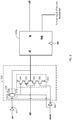
- FIG. 2 shows an exemplary implementation of the first scan multiplexer 110a and the first D flip-flip 120a.
- the first scan multiplexer 110a comprises a first tri-state circuit 215 and a second tri-state circuit 220, in which each tri-state circuit includes four transistors (e.g., metal-oxide-semiconductor (MOS) transistors).
- MOS metal-oxide-semiconductor
- the first and second tri-state circuits 215 and 220 are controlled by the scan mode signal received at the scan mode input (labeled "scan" in FIG. 2 ).
- the tri-state circuits 215 and 220 operate in the normal mode when the scan mode signal is zero, and operate in the scan mode when the scan mode signal is one.
- the first tri-state circuit 215 inverts the respective input data signal
- the second tri-state circuit 220 passes the inverted data signal to the input of the respective D flip-flop 120a.
- the D flip-flop 120a has an odd number of inverters (i.e., inverters 232, 234 and 236) between its input and q output.
- the odd number of inverters undoes the logical inversion by the first tri-state circuit 215.
- the first tri-state circuit 215 blocks the respective data input.
- the second tri-state circuit 220 inverts the respective input scan signal, and inputs the inverted scan signal to the respective D flip-flop 120a.
- the D flip-flop 120a has an even number of inverters (i.e., inverters 232 and 234) between its input and nq output. As a result, there is a logical inversion from the scan input of the multiplexer 110a to the nq output of the D flip-flop 120a.
- the scan multiplexer 110a in FIG. 2 inverts the input data signal before outputting the data signal to the respective flip-flop 120a.
- the scan multiplexer 110a in the scan mode inverts the input scan signal before outputting the scan signal to the respective flip-flop 120a.
- the scan multiplexer 110a in FIG. 2 is an example of an inverting multiplexer.
- Each of the remaining scan multiplexers 110b-110d in the flop tray 100 can also be implemented using the circuit shown in FIG. 2 .
- the scan input of the multiplexer (labeled "1" in FIG. 1 ) is coupled to the nq output of the previous D flip-flop 120a-120c.
- the transistors making up the first and second tri-state circuits 215 and 220 of each scan multiplexer 110a-110d take up chip area and consume power. Accordingly, it is desirable to reduce the number of transistors in the multiplexers in order to reduce the area and/or power consumption of the scan circuitry 115.
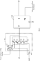
- FIG. 3 shows a scan multiplexer 310 according to an embodiment of the present disclosure.
- FIG. 3 shows an example in which the scan multiplexer 310 is used to implement the first scan multiplexer in a flop tray, which is coupled between the scan input ("sin") of the flop tray and the first flip-flop 120a of the flop tray.
- An example of a flop tray including scan multiplexers implemented using the scan multiplexer 310 shown in FIG. 3 is discussed below with reference to FIG. 5 .
- the second tri-state circuit 220 in the scan multiplexer 110a shown in FIG. 2 is replaced by a pass gate 320.
- the pass gate 320 comprises two transistors compared with four transistors for the second tri-state circuit 220, resulting in a reduction of two transistors in the scan multiplexer 310.
- the pass gate 320 comprises an n-type transistor 322 and a p-type transistor 324 coupled in parallel, in which the gate of the n-type transistor 322 is coupled to the scan mode input (“scan”) and the gate of the p-type transistor 324 is coupled to the scan mode input ("scan") through a scan mode inverter 360.
- the gate of the n-type transistor 322 is driven by the scan mode signal and the gate of the p-type transistor 324 is driven by the inverse of the scan mode signal. Both transistors 322 and 324 are turned on in the scan mode and both transistors 322 and 324 are turned off in the normal mode.
- the first tri-state circuit 215 When the scan mode signal is zero (normal mode), the first tri-state circuit 215 inverts the input data signal, and outputs the inverted data signal to the input of the first flip-flop 120a of the flop tray.
- the first tri-state circuit 215 is described in more detail below.
- the pass gate 320 blocks the input scan signal from the input of the first D flip-flop 120a.
- the scan multiplexer 310 is functionally equivalent to the first scan multiplexer 110a shown in FIG. 2 .
- the first tri-state circuit 215 blocks the input data signal from the input of the first D flip-flop 120a.
- the pass gate 320 passes the input scan signal to the input of the first D flip-flop 120a.
- the pass gate 320 does not invert the input scan signal unlike the second tri-state circuit 220 in the first multiplexer 110a shown in FIG. 2 .
- the scan multiplexer 310 passes the scan signal to the first flip-flop 120a without inversion.
- an inverter 315 may be coupled between the scan input ("sin") of the flop tray and the scan multiplexer 310 to invert the scan signal prior to being input to the scan multiplexer 310.
- the combination of the inverter 315 and the pass gate 320 in the scan multiplexer 310 may be functionally equivalent to the second tri-state circuit 220 shown in FIG. 2 .
- Each of the remaining scan multiplexers in the flop tray can also be implemented using the multiplexer 310 shown in FIG. 3 .
- the input of the pass gate 320 may be coupled to the nq output of the previous D flip-flop without an intervening inverter.
- FIG. 4 shows an example in which the scan multiplexer 310 is used to implement the second scan multiplexer in a flop tray.
- the pass gate 320 is coupled to the nq output of the first D flip-flop 120a (shown in FIG. 3 ) without an intervening inverter. As discussed above, the pass gate 320 replaces the second tri-state circuit 220 shown in FIG. 2 , resulting in a reduction of two transistors in the multiplexer 310.
- the first tri-state circuit 215 Inverts the input data signal, and outputs the inverted data signal to the input of the second D flip-flop 120b of the flop tray.
- the pass gate 320 blocks the scan signal from the input of the second D flip-flop 120b.
- the first tri-state circuit 215 blocks the input data signal from the input of the second D flip-flop 120b.
- the pass gate 320 passes the scan signal from the nq output of the first D flip-flop 120a (shown in FIG. 3 ) to the input of the second D flip-flop 120b.
- the scan signal from the nq output of the second D flip-flop 120b is coupled to the third scan multiplexer in the flop tray.
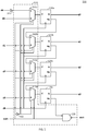
- FIG. 5 shows an example of a scannable flop tray 500, in which the scan circuitry 115 in FIG. 1 is replaced by scan circuitry 515 according to an embodiment of the present disclosure.
- the scan circuitry 515 comprises a first scan multiplexer 310a, a second scan multiplexer 310b, a third scan multiplexer 310c, and a fourth scan multiplexer 310d, in which each of the scan multiplexers 310a-310d is implemented using the scan multiplexer 310 shown in FIG. 3 .
- the scan circuitry 515 also comprises the scan mode inverter 360, which is shared by the scan multiplexers 310a-310d.
- the scan mode inverter 360 provides each scan multiplexer 310a-310d with the inverse of the scan mode signal.
- the flop tray 500 also comprises the inverter 315 coupled between the scan input (“sin") of the flop tray 500 and the scan input (labeled "1") of the first scan multiplexer 310a.
- the scan input (labeled “1") of the first scan multiplexer 310 is coupled to the inverter 315.
- the scan input (labeled "1") of each of the remaining scan multiplexers 310b-310d is coupled to the nq output of the previous D flip-flop 120a-120c without an intervening inverter.
- the data input (labeled "0") of each of the scan multiplexers 310a-310d is coupled to the respective data signal d0-d3, and the output of each of the scan multiplexers 310a-310d is coupled to the input of the respective flip-flop 120a-120d.
- each scan multiplexer 310a-310d inverts the respective data signal d0-d3 using the respective tri-state circuit 215, and outputs the inverted data signal to the input of the respective D flip-flop 120a-120d.
- Each D flip-flop 120a-120d captures a data value (e.g., a bit) from the respective data signal d0-d3 on a rising or falling edge of a clock signal clk, and outputs the captured data value q0-q3.
- the inverter 315 inverts the scan signal at the scan input ("sin") of the flop tray 500 to generate an inverted input scan signal.
- the first scan multiplexer 310a passes the inverted input scan signal to the input of the first D flip-flop 120a.
- Each of the remaining scan multiplexers 310b-310c couples the scan signal output from the previous flip-flop 120a-120c to the input of the respective flip-flop 120b-120d without inversion.
- the scan signal is finally output at the output of the NAND gate 130 (labeled "sout”).
- the output scan signal may be inverted or non-inverted relative to the input scan signal depending on the number of inversions in the scan path from the scan input ("sin") of the flop tray 500 to the scan output ("sout").
- a scan signal is scanned through the D flip-flops 120a-120d of the flop tray 500.
- the scan signal may comprise a known test pattern, and the functionality of the flop tray 500 may be evaluated by comparing the output scan signal from the flop tray 500 with an expected output scan signal based on the known test pattern.
- the expected output scan signal for the flop tray 500 in FIG. 5 may differ from the expected output scan signal for the flop tray 100 in FIG. 1 for a given test pattern. This is because the flop tray 500 in FIG. 5 has a different number of inversions in the scan path due to the fact that the scan multiplexers 310a-310d do not invert the scan signal.
- each scan multiplexer 310a-310d of the flop tray 500 using the multiplexer 310 shown in FIG. 3 can lead to a significant reduction in the number of transistors in the flop tray 500.
- the first scan multiplexer 310a in the flop tray 500 may not contribute to a reduction in the number of transistors because of the inverter 315 coupled between the scan input ("sin") of the flop tray 500 and the first scan multiplexer 310a.
- each of the remaining scan multiplexers 310b-310d in the flop tray 500 reduces the transistor count by two. This is because, for each of the remaining scan multiplexers 310b-310d, the respective pass gate 320 uses two transistors compared with four transistors for the second tri-state circuit 220 shown in FIG.
- each D flip-flop 120a-120d In order for each D flip-flop 120a-120d to properly capture a value from a signal (e.g., the respective data signal d0-d3 or scan signal) at its input, the value needs to stable for a period of time after a rising or falling edge of the clock clk (referred to as hold time). If the signal changes value during the hold time, then a hold time violation occurs and the flip-flop may enter into a metastable state. To prevent a hold time violation in the normal mode, the delay in the data path to the flip-flop may be adjusted to provide a sufficient hold time margin at the input of the flip-flop.
- the hold time margin may be the difference between an expected time for a change in the signal after the rising or falling edge of the clock clk and the hold time. A larger hold time margin improves the robustness of the flip-flop by providing a larger margin for process and operating variations.
- the hold time margin for each of the second, third and fourth flip-flops 120b-120d in FIG. 5 is reduced by approximately one inverter delay compared with the second, third and fourth flip-flops 120b-120d in FIG. 1 .
- each of the respective multiplexers 310b-310d in FIG. 5 does not invert the scan signal unlike the respective multiplexers 110b-110d in FIG. 1 .
- the hold time margin may remain sufficiently large to prevent hold time violations during testing.
- the hold time margin for the first flip-flop 120a may be approximately the same since the inverter 315 coupled to the first multiplexer 110a adds an inverter delay.
- the first tri-state circuit 215 is an example of a tri-state inverter, and comprises a first p-type transistor 330, a second p-type transistor 335, a first n-type transistor 350, and a second n-type transistor 340.
- the transistors 330, 335, 340 and 350 are stacked on top of one another between a power supply and ground.
- the source of the first p-type transistor 330 is coupled to the power supply
- the source of the second p-type transistor 335 is coupled to the drain of the first p-type transistor 330
- the drain of the second n-type transistor 340 is coupled to the drain of the second p-type transistor 335
- the drain of the first n-type transistor 350 is coupled to the source of the second n-type transistor 340
- the source of the first n-type transistor 350 is coupled to ground.
- the gate of the first p-type transistor 330 is coupled to the scan mode input ("scan") and the gate of the first n-type transistor 350 is coupled to the scan mode input (“scan") through the scan mode inverter 360, which may be shared by the scan multiplexers 310a-310d, as shown in FIG. 5 .
- the gate of the first p-type transistor 330 is driven by the scan mode signal
- the gate of the first n-type transistor 350 is driven by the inverse of the scan mode signal.
- the gates of the second p-type transistor 335 and the second n-type transistor 340 are coupled to the data input of the multiplexer 310.
- the first p-type transistor 330 and the first n-type transistor 350 are both turned on.
- the first p-type transistor 330 couples the source of the second p-type transistor 335 to the power supply
- the first n-type 350 couples the source of the second n-type transistor 340 to ground.
- the second p-type transistor 335 and the second n-type transistor 340 act as a complimentary inverter, in which the input of the inverter is located at the gates of the second p-type transistor 335 and the second n-type transistor 340, and the output of the inverter is located at the drains of the second p-type transistor 335 and the second n-type transistor 340.
- the inverter inverts the respective data signal and outputs the inverted data signal to the respective flip-flop.
- the first p-type transistor 330 and the first n-type transistor 350 are both turned off. This disconnects the source of the second p-type transistor 335 from the power supply, and disconnects the source of the second n-type transistor 340 from ground. As a result, the respective data signal is blocked from the input of the respective flip-flop.
- FIG. 6 is a flow diagram of a method 600 for scanning a flop tray with reduced scan overhead according to an embodiment of the present disclosure.
- step 610 an input data signal is inverted and outputted to an input of a flip-flop in a normal mode using a tri-state circuit.
- step 610 may be performed using the tri-state circuit 215 in FIG. 3 , in which the tri-state circuit 215 is operated in the normal mode by inputting a scan mode signal of zero to the scan mode input ("scan").
- step 620 the input data signal is blocked from the input of the flip-flop in a scan mode using the tri-state circuit.
- step 620 may be performed using the tri-state circuit 215 in FIG. 3 , in which the tri-state circuit 215 is operated in the scan mode by inputting a scan mode signal of one to the scan mode input ("scan").
- step 630 a scan signal is passed to the input of the flip-flop in the scan mode using a pass gate.
- step 630 may be performed using the pass gate 320 in FIG. 3 , in which the pass gate 320 is operated in the scan mode by inputting a scan mode signal of one to the scan mode input ("scan").
- the pass gate 320 may be implemented using fewer transistors than a tri-state circuit, and therefore reduce the scan overhead.
- step 640 the scan signal is blocked from the input of the flip-flop in the normal mode using the pass gate.
- step 640 may be performed using the pass gate 320 in FIG. 3 , in which the pass gate 320 is operated in the normal mode by inputting a scan mode signal of zero to the scan mode input ("scan").
- embodiments of the present disclosure are not limited to the examples described herein.
- the scan input of a scan multiplexer may be coupled to the q output of the previous flip-flop instead of the nq output.
- embodiments of the present disclosure may be used in flop trays comprising various types of flip-flops, and therefore are not limited to the exemplary flip-flop shown in FIG. 2 .
- embodiments of the present disclosure may be used in flop trays comprising any number of flip-flops, including, for example, two flip-flops, four flip-flops, 8 flip-flops, 16 flip-flops, etc.
- circuits described herein may be realized using a variety of transistor types, and are therefore not limited to the particular transistor types shown in the figures.
- transistor types such as bipolar junction transistors, junction field effect transistor or any other transistor type may be used.
- circuits described herein may be fabricated with various IC process technologies such as CMOS, bipolar junction transistor (BJT), bipolar-CMOS (BiCMOS), silicon germanium (SiGe), gallium arsenide (GaAs), etc.
Claims (15)
- Eine Scan-Schaltung (515) für ein Flop-Tray (500), die Folgendes aufweist:eine Tri-State-Schaltung bzw. Schaltung (215) mit drei Zuständen, die konfiguriert ist zum Invertieren eines Eingangsdatensignals und zum Ausgeben des invertierten Datensignals an einen Eingang eines Flip-Flops (120b) in einem normalen Modus, und zum Blockieren des Datensignals von dem Eingang des Flipflop des Flop-Tray in einem Scan-Modus; undein Pass- bzw. Durchlass-Gate (320), das konfiguriert ist zum Durchlassen bzw. Weiterleiten eines Scan-Signals an den Eingang des Flip-Flops in dem Scan-Modus und zum Blockieren des Scan-Signals hinsichtlich des Eingangs des Flip-Flops in dem normalen Modus.
- Scan-Schaltung (515) nach Anspruch 1, wobei das Durchlass-Gate (320) Folgendes aufweist:einen n-Typ-Transistor (322); undeinen p-Typ-Transistor (324), der parallel zu dem n-Typ-Transistor gekoppelt ist, wobei der p-Typ-Transistor und der n-Typ-Transistor konfiguriert sind zum Anschalten in dem Scan-Modus und zum Abschalten in dem normalen Modus.
- Scan-Schaltung (515) nach Anspruch 1, die weiter einen Inverter (360) aufweist, der zwischen einen Scan-Eingang des Flop-Tray (500) und das Durchlass-Gate (320) gekoppelt ist.
- Scan-Schaltung (515) nach Anspruch 1, wobei das Durchlass-Gate (320) zwischen einen Ausgang eines weiteren Flip-Flops (120a) des Flop-Tray und den Eingang des Flip-Flops (120b) gekoppelt ist.
- Scan-Schaltung (515) nach Anspruch 4, wobei es keinen Inverter (315) zwischen dem Ausgang des weiteren Flipflop und dem Durchlass-Gate gibt.
- Scan-Schaltung (515) nach Anspruch 1, die weiter Folgendes aufweist:eine zweite Tri-State-Schaltung bzw. Schaltung mit drei Zuständen, die konfiguriert ist zum Invertieren eines zweiten Datensignals und Ausgeben des invertierten zweiten Datensignals an einen Eingang eines zweiten Flip-Flop (120c) des Flop-Tray in dem normalen Modus und zum Blockieren des zweiten Datensignals von dem Eingang des zweiten Flip-Flop in dem Scan-Modus; undein zweites Pass- bzw. Durchlass-Gate, das konfiguriert ist zum Durchlassen bzw. Weiterleiten des Scan-Signals von einem Ausgang des Flip-Flop an den Eingang des zweiten Flip-Flop in dem Scan-Modus und zum Blockieren des Scan-Signals von dem Ausgang des Flip-Flops hinsichtlich des Eingangs des zweiten Flip-Flop in den normalen Modus.
- Scan-Schaltung (515) nach Anspruch 6, wobei es keinen Inverter zwischen dem Ausgang des Flip-Flops und dem zweiten Durchlass-Gate gibt.
- Scan-Schaltung (515) nach Anspruch 6, die weiter einen Inverter aufweist, der zwischen einen Scan-Eingang des Flop-Tray (500) und das Durchlass-Gate gekoppelt ist.
- Scan-Schaltung (515) nach Anspruch 8, wobei es keinen Inverter zwischen dem Ausgang des Flip-Flops und dem zweiten Durchlass-Gate gibt.
- Scan-Schaltung (515) nach Anspruch 9, wobei das zweite Durchlass-Gate Folgendes aufweist:einen n-Typ-Transistor; undeinen p-Typ-Transistor, der parallel zu dem n-Typ-Transistor gekoppelt ist,wobei der p-Typ-Transistor und der n-Typ-Transistor konfiguriert sind zum Anschalten in dem Scan-Modus und zum Abschalten in dem normalen Modus.
- Ein Verfahren (600) zum Scannen eines Flop-Tray (500), das Folgendes aufweist.
Invertieren (610) eines Eingangsdatensignals und Ausgeben des invertierten Datensignals an einen Eingang eines Flip-Flops (120a) des Flop-Tray in einem normalen Modus unter Verwendung einer Tri-State-Schaltung bzw. Schaltung (215) mit drei Zuständen;
Blockieren (620) des Datensignals von dem Eingang des Flip-Flops (120a) in einem Scan-Modus unter Verwendung der Schaltung (215) mit drei Zuständen;
Durchlassen bzw. Weiterleiten (630) eines Scan-Signals an den Eingang des Flip-Flops (120a) in dem Scan-Modus unter Verwendung eines Pass- bzw. Durchlass-Gates (320); und
Blockieren (640) des Scan-Signals von dem Eingang des Flip-Flops (120a) in dem normalen Modus unter Verwendung des Durchlass-Gates (320). - Verfahren (600) nach Anspruch 11, das weiter Durchlassen der Scan-Signalausgabe von dem Flip-Flop (120a) an einen Eingang eines weiteren Flip-Flops (120b) des Flop-Tray in dem Scan-Modus unter Verwendung eines weiteren Durchlass-Gates aufweist.
- Verfahren (600) nach Anspruch 12, wobei die Scan-Signalausgabe von dem Flip-Flop an den Eingang des weiteren Flip-Flops (120b) ohne Invertieren der Scan-Signalausgabe von dem Flip-Flop durchgelassen bzw. weitergeleitet wird.
- Verfahren (600) nach Anspruch 11, das weiter Invertieren des Scan-Signals vor dem Durchlassen bzw. Weiterleiten des Scan-Signals an den Eingang des Flipflop-Flops unter Verwendung des Durchlass-Gates (320) aufweist.
- Verfahren (600) nach Anspruch 14, das weiter Durchlassen bzw. Weiterleiten der Scan-Signalausgabe von dem Flip-Flop an einen Eingang eines weiteren Flip-Flops des Flop-Tray in dem Scan-Modus unter Verwendung eines weiteren Durchlass-Gates aufweist, wobei die Scan-Signalausgabe von dem Flip-Flop an den Eingang des weiteren Flip-Flops ohne Invertieren der Scan-Signalausgabe von dem Flip-Flop durchgelassen bzw. weitergeleitet wird.
Applications Claiming Priority (2)
| Application Number | Priority Date | Filing Date | Title |
|---|---|---|---|
| US13/905,060 US9024658B2 (en) | 2013-05-29 | 2013-05-29 | Circuit and layout techniques for flop tray area and power otimization |
| PCT/US2014/039856 WO2014193998A1 (en) | 2013-05-29 | 2014-05-28 | Circuit and layout techniques for flop tray area and power optimization |
Publications (2)
| Publication Number | Publication Date |
|---|---|
| EP3004903A1 EP3004903A1 (de) | 2016-04-13 |
| EP3004903B1 true EP3004903B1 (de) | 2017-05-03 |
Family
ID=51022458
Family Applications (1)
| Application Number | Title | Priority Date | Filing Date |
|---|---|---|---|
| EP14733455.1A Active EP3004903B1 (de) | 2013-05-29 | 2014-05-28 | Schaltung und layouttechniken für bereichs- und leistungsoptimierung für flop-tray |
Country Status (6)
| Country | Link |
|---|---|
| US (1) | US9024658B2 (de) |
| EP (1) | EP3004903B1 (de) |
| JP (1) | JP6337099B2 (de) |
| KR (1) | KR20160016890A (de) |
| CN (1) | CN105247377B (de) |
| WO (1) | WO2014193998A1 (de) |
Families Citing this family (6)
| Publication number | Priority date | Publication date | Assignee | Title |
|---|---|---|---|---|
| JP6268461B2 (ja) | 2013-03-28 | 2018-01-31 | セイコーエプソン株式会社 | 半導体装置、物理量センサー、電子機器及び移動体 |
| US9685141B2 (en) * | 2014-01-31 | 2017-06-20 | Samsung Display Co., Ltd. | MDLL/PLL hybrid design with uniformly distributed output phases |
| US10033359B2 (en) | 2015-10-23 | 2018-07-24 | Qualcomm Incorporated | Area efficient flip-flop with improved scan hold-margin |
| US9966953B2 (en) | 2016-06-02 | 2018-05-08 | Qualcomm Incorporated | Low clock power data-gated flip-flop |
| US11092646B1 (en) * | 2020-02-18 | 2021-08-17 | Qualcomm Incorporated | Determining a voltage and/or frequency for a performance mode |
| US11500016B2 (en) * | 2020-12-07 | 2022-11-15 | Taiwan Semiconductor Manufacturing Company Ltd. | Circuit screening system and circuit screening method |
Family Cites Families (32)
| Publication number | Priority date | Publication date | Assignee | Title |
|---|---|---|---|---|
| US5444404A (en) | 1994-03-03 | 1995-08-22 | Vlsi Technology, Inc. | Scan flip-flop with power saving feature |
| AU2204695A (en) * | 1994-04-28 | 1995-11-29 | Apple Computer, Inc. | Scannable d-flip-flop with system independent clocking |
| JPH09270677A (ja) * | 1995-09-05 | 1997-10-14 | Mitsubishi Electric Corp | フリップフロップ回路及びスキャンパス並びに記憶回路 |
| US5719878A (en) | 1995-12-04 | 1998-02-17 | Motorola Inc. | Scannable storage cell and method of operation |
| JPH1052073A (ja) * | 1996-07-31 | 1998-02-20 | Seiko Kurotsuku Kk | 超音波モータの駆動回路 |
| JPH1194914A (ja) | 1997-09-22 | 1999-04-09 | Matsushita Electric Ind Co Ltd | スキャンパス制御回路 |
| US6708303B1 (en) | 1998-03-06 | 2004-03-16 | Texas Instruments Incorporated | Method and apparatus for controlling a seperate scan output of a scan circuit |
| US6289477B1 (en) * | 1998-04-28 | 2001-09-11 | Adaptec, Inc. | Fast-scan-flop and integrated circuit device incorporating the same |
| US6420894B1 (en) | 1999-12-29 | 2002-07-16 | Intel Corporation | Implementation of iscan cell for self-resetting dynamic circuit |
| JP3928938B2 (ja) * | 2002-05-28 | 2007-06-13 | シャープ株式会社 | 電圧変換回路および半導体装置 |
| JP2004069492A (ja) * | 2002-08-06 | 2004-03-04 | Renesas Technology Corp | フリップフロップ回路 |
| US7237164B1 (en) | 2004-04-15 | 2007-06-26 | Marvell International Ltd. | Area optimized edge-triggered flip-flop for high-speed memory dominated design |
| JP2006005661A (ja) * | 2004-06-17 | 2006-01-05 | Matsushita Electric Ind Co Ltd | フリップフロップ回路 |
| KR101076809B1 (ko) * | 2004-06-18 | 2011-10-25 | 삼성전자주식회사 | 불필요한 전력소모를 줄일 수 있는 스캔 플립플롭 회로 |
| US20060085707A1 (en) * | 2004-09-28 | 2006-04-20 | Texas Instruments Incorporated | High speed energy conserving scan architecture |
| KR100604904B1 (ko) | 2004-10-02 | 2006-07-28 | 삼성전자주식회사 | 스캔 입력을 갖는 플립 플롭 회로 |
| US7315191B2 (en) * | 2005-06-30 | 2008-01-01 | Texas Instruments Incorporated | Digital storage element architecture comprising dual scan clocks and reset functionality |
| US7543205B2 (en) * | 2006-04-27 | 2009-06-02 | Texas Instruments Incorporated | Control signal synchronization of a scannable storage circuit |
| US7793178B2 (en) | 2006-07-12 | 2010-09-07 | Texas Instruments Incorporated | Cell supporting scan-based tests and with reduced time delay in functional mode |
| US7649395B2 (en) | 2007-05-15 | 2010-01-19 | Ati Technologies Ulc | Scan flip-flop with internal latency for scan input |
| JP4999632B2 (ja) * | 2007-10-12 | 2012-08-15 | オンセミコンダクター・トレーディング・リミテッド | 半導体集積回路 |
| KR20090131010A (ko) * | 2008-06-17 | 2009-12-28 | 주식회사 동부하이텍 | 듀얼 모드 에지 트리거 플립플롭 |
| US7893722B2 (en) * | 2008-09-11 | 2011-02-22 | Arm Limited | Clock control of state storage circuitry |
| CN102062836B (zh) * | 2009-11-17 | 2013-02-06 | 三星半导体(中国)研究开发有限公司 | 扫描寄存器、扫描链、芯片及其测试方法 |
| US20110181331A1 (en) * | 2010-01-24 | 2011-07-28 | Freescale Semiconductor, Inc. | Integrated circuit with leakage reduction in static nets |
| US8427214B2 (en) * | 2010-06-03 | 2013-04-23 | Arm Limited | Clock state independent retention master-slave flip-flop |
| CN103004088B (zh) * | 2010-07-16 | 2016-04-13 | 马维尔国际贸易有限公司 | 电荷注入感测放大器电路 |
| US8493119B2 (en) * | 2010-12-13 | 2013-07-23 | Apple Inc. | Scannable flip-flop with hold time improvements |
| US8502561B2 (en) * | 2011-07-01 | 2013-08-06 | Arm Limited | Signal value storage circuitry with transition detector |
| US8578224B2 (en) * | 2011-12-31 | 2013-11-05 | Texas Instruments Incorporated | High density flip-flop with asynchronous reset |
| CN103576082B (zh) * | 2012-08-06 | 2018-01-12 | 恩智浦美国有限公司 | 低功率扫描触发器单元 |
| US9020084B2 (en) * | 2013-01-31 | 2015-04-28 | Qualcomm Incorporated | High frequency synchronizer |
-
2013
- 2013-05-29 US US13/905,060 patent/US9024658B2/en active Active
-
2014
- 2014-05-28 WO PCT/US2014/039856 patent/WO2014193998A1/en active Application Filing
- 2014-05-28 EP EP14733455.1A patent/EP3004903B1/de active Active
- 2014-05-28 JP JP2016516796A patent/JP6337099B2/ja active Active
- 2014-05-28 KR KR1020157036440A patent/KR20160016890A/ko not_active Application Discontinuation
- 2014-05-28 CN CN201480030877.3A patent/CN105247377B/zh active Active
Also Published As
| Publication number | Publication date |
|---|---|
| WO2014193998A1 (en) | 2014-12-04 |
| CN105247377B (zh) | 2018-02-09 |
| EP3004903A1 (de) | 2016-04-13 |
| JP6337099B2 (ja) | 2018-06-06 |
| KR20160016890A (ko) | 2016-02-15 |
| CN105247377A (zh) | 2016-01-13 |
| US20140359385A1 (en) | 2014-12-04 |
| JP2016531275A (ja) | 2016-10-06 |
| US9024658B2 (en) | 2015-05-05 |
Similar Documents
| Publication | Publication Date | Title |
|---|---|---|
| EP3004903B1 (de) | Schaltung und layouttechniken für bereichs- und leistungsoptimierung für flop-tray | |
| US6968486B2 (en) | Master-slave-type scanning flip-flop circuit for high-speed operation with reduced load capacity of clock controller | |
| US10931264B2 (en) | Low-power flip flop circuit | |
| US7590900B2 (en) | Flip flop circuit & same with scan function | |
| US8880965B2 (en) | Low power scan flip-flop cell | |
| US7358786B2 (en) | Control signal generator, latch circuit, flip flop and method for controlling operations of the flip-flop | |
| US8484523B2 (en) | Sequential digital circuitry with test scan | |
| US7345519B2 (en) | Flip-flop circuit | |
| US20090300448A1 (en) | Scan flip-flop device | |
| US7859310B2 (en) | Semiconductor integrated circuit | |
| KR20100047191A (ko) | 스캔 입력에 대한 내부 지연을 가진 스캔 플립플롭 | |
| US20090309641A1 (en) | Dual mode edge triggered flip-flop | |
| US6380780B1 (en) | Integrated circuit with scan flip-flop | |
| JP3878236B2 (ja) | フリップフロップ制御器 | |
| KR950024305A (ko) | 논리합성방법 및 반도체집적회로 | |
| US9979381B1 (en) | Semi-data gated flop with low clock power/low internal power with minimal area overhead | |
| JP3802377B2 (ja) | フリップフロップ及びスキャンパス回路 | |
| US11366162B2 (en) | Scan output flip-flop with power saving feature | |
| US7663408B2 (en) | Scannable dynamic circuit latch | |
| US20110016367A1 (en) | Skew tolerant scannable master/slave flip-flop including embedded logic | |
| JP2019036622A (ja) | 記憶回路及び記憶回路の制御方法 | |
| CN112583382A (zh) | 正反器 | |
| Chakraborty et al. | Novel Self-Timed, Pipelined Clock Scan Architecture | |
| JPWO2002047267A1 (ja) | 半導体集積回路装置 |
Legal Events
| Date | Code | Title | Description |
|---|---|---|---|
| PUAI | Public reference made under article 153(3) epc to a published international application that has entered the european phase |
Free format text: ORIGINAL CODE: 0009012 |
|
| 17P | Request for examination filed |
Effective date: 20151022 |
|
| AK | Designated contracting states |
Kind code of ref document: A1 Designated state(s): AL AT BE BG CH CY CZ DE DK EE ES FI FR GB GR HR HU IE IS IT LI LT LU LV MC MK MT NL NO PL PT RO RS SE SI SK SM TR |
|
| AX | Request for extension of the european patent |
Extension state: BA ME |
|
| DAX | Request for extension of the european patent (deleted) | ||
| GRAP | Despatch of communication of intention to grant a patent |
Free format text: ORIGINAL CODE: EPIDOSNIGR1 |
|
| RIC1 | Information provided on ipc code assigned before grant |
Ipc: G01R 31/3177 20060101ALI20161027BHEP Ipc: G01R 31/3185 20060101AFI20161027BHEP |
|
| INTG | Intention to grant announced |
Effective date: 20161121 |
|
| GRAS | Grant fee paid |
Free format text: ORIGINAL CODE: EPIDOSNIGR3 |
|
| GRAA | (expected) grant |
Free format text: ORIGINAL CODE: 0009210 |
|
| AK | Designated contracting states |
Kind code of ref document: B1 Designated state(s): AL AT BE BG CH CY CZ DE DK EE ES FI FR GB GR HR HU IE IS IT LI LT LU LV MC MK MT NL NO PL PT RO RS SE SI SK SM TR |
|
| REG | Reference to a national code |
Ref country code: GB Ref legal event code: FG4D Ref country code: FR Ref legal event code: PLFP Year of fee payment: 4 |
|
| REG | Reference to a national code |
Ref country code: AT Ref legal event code: REF Ref document number: 890581 Country of ref document: AT Kind code of ref document: T Effective date: 20170515 Ref country code: CH Ref legal event code: EP |
|
| REG | Reference to a national code |
Ref country code: IE Ref legal event code: FG4D |
|
| REG | Reference to a national code |
Ref country code: DE Ref legal event code: R096 Ref document number: 602014009423 Country of ref document: DE |
|
| REG | Reference to a national code |
Ref country code: NL Ref legal event code: MP Effective date: 20170503 |
|
| REG | Reference to a national code |
Ref country code: AT Ref legal event code: MK05 Ref document number: 890581 Country of ref document: AT Kind code of ref document: T Effective date: 20170503 |
|
| REG | Reference to a national code |
Ref country code: LT Ref legal event code: MG4D |
|
| PG25 | Lapsed in a contracting state [announced via postgrant information from national office to epo] |
Ref country code: GR Free format text: LAPSE BECAUSE OF FAILURE TO SUBMIT A TRANSLATION OF THE DESCRIPTION OR TO PAY THE FEE WITHIN THE PRESCRIBED TIME-LIMIT Effective date: 20170804 Ref country code: ES Free format text: LAPSE BECAUSE OF FAILURE TO SUBMIT A TRANSLATION OF THE DESCRIPTION OR TO PAY THE FEE WITHIN THE PRESCRIBED TIME-LIMIT Effective date: 20170503 Ref country code: LT Free format text: LAPSE BECAUSE OF FAILURE TO SUBMIT A TRANSLATION OF THE DESCRIPTION OR TO PAY THE FEE WITHIN THE PRESCRIBED TIME-LIMIT Effective date: 20170503 Ref country code: AT Free format text: LAPSE BECAUSE OF FAILURE TO SUBMIT A TRANSLATION OF THE DESCRIPTION OR TO PAY THE FEE WITHIN THE PRESCRIBED TIME-LIMIT Effective date: 20170503 Ref country code: HR Free format text: LAPSE BECAUSE OF FAILURE TO SUBMIT A TRANSLATION OF THE DESCRIPTION OR TO PAY THE FEE WITHIN THE PRESCRIBED TIME-LIMIT Effective date: 20170503 Ref country code: NO Free format text: LAPSE BECAUSE OF FAILURE TO SUBMIT A TRANSLATION OF THE DESCRIPTION OR TO PAY THE FEE WITHIN THE PRESCRIBED TIME-LIMIT Effective date: 20170803 Ref country code: FI Free format text: LAPSE BECAUSE OF FAILURE TO SUBMIT A TRANSLATION OF THE DESCRIPTION OR TO PAY THE FEE WITHIN THE PRESCRIBED TIME-LIMIT Effective date: 20170503 |
|
| PG25 | Lapsed in a contracting state [announced via postgrant information from national office to epo] |
Ref country code: LV Free format text: LAPSE BECAUSE OF FAILURE TO SUBMIT A TRANSLATION OF THE DESCRIPTION OR TO PAY THE FEE WITHIN THE PRESCRIBED TIME-LIMIT Effective date: 20170503 Ref country code: BG Free format text: LAPSE BECAUSE OF FAILURE TO SUBMIT A TRANSLATION OF THE DESCRIPTION OR TO PAY THE FEE WITHIN THE PRESCRIBED TIME-LIMIT Effective date: 20170803 Ref country code: NL Free format text: LAPSE BECAUSE OF FAILURE TO SUBMIT A TRANSLATION OF THE DESCRIPTION OR TO PAY THE FEE WITHIN THE PRESCRIBED TIME-LIMIT Effective date: 20170503 Ref country code: PL Free format text: LAPSE BECAUSE OF FAILURE TO SUBMIT A TRANSLATION OF THE DESCRIPTION OR TO PAY THE FEE WITHIN THE PRESCRIBED TIME-LIMIT Effective date: 20170503 Ref country code: SE Free format text: LAPSE BECAUSE OF FAILURE TO SUBMIT A TRANSLATION OF THE DESCRIPTION OR TO PAY THE FEE WITHIN THE PRESCRIBED TIME-LIMIT Effective date: 20170503 Ref country code: RS Free format text: LAPSE BECAUSE OF FAILURE TO SUBMIT A TRANSLATION OF THE DESCRIPTION OR TO PAY THE FEE WITHIN THE PRESCRIBED TIME-LIMIT Effective date: 20170503 Ref country code: IS Free format text: LAPSE BECAUSE OF FAILURE TO SUBMIT A TRANSLATION OF THE DESCRIPTION OR TO PAY THE FEE WITHIN THE PRESCRIBED TIME-LIMIT Effective date: 20170903 |
|
| REG | Reference to a national code |
Ref country code: CH Ref legal event code: PL |
|
| PG25 | Lapsed in a contracting state [announced via postgrant information from national office to epo] |
Ref country code: DK Free format text: LAPSE BECAUSE OF FAILURE TO SUBMIT A TRANSLATION OF THE DESCRIPTION OR TO PAY THE FEE WITHIN THE PRESCRIBED TIME-LIMIT Effective date: 20170503 Ref country code: SK Free format text: LAPSE BECAUSE OF FAILURE TO SUBMIT A TRANSLATION OF THE DESCRIPTION OR TO PAY THE FEE WITHIN THE PRESCRIBED TIME-LIMIT Effective date: 20170503 Ref country code: EE Free format text: LAPSE BECAUSE OF FAILURE TO SUBMIT A TRANSLATION OF THE DESCRIPTION OR TO PAY THE FEE WITHIN THE PRESCRIBED TIME-LIMIT Effective date: 20170503 Ref country code: CZ Free format text: LAPSE BECAUSE OF FAILURE TO SUBMIT A TRANSLATION OF THE DESCRIPTION OR TO PAY THE FEE WITHIN THE PRESCRIBED TIME-LIMIT Effective date: 20170503 Ref country code: RO Free format text: LAPSE BECAUSE OF FAILURE TO SUBMIT A TRANSLATION OF THE DESCRIPTION OR TO PAY THE FEE WITHIN THE PRESCRIBED TIME-LIMIT Effective date: 20170503 |
|
| REG | Reference to a national code |
Ref country code: DE Ref legal event code: R097 Ref document number: 602014009423 Country of ref document: DE |
|
| REG | Reference to a national code |
Ref country code: IE Ref legal event code: MM4A |
|
| PG25 | Lapsed in a contracting state [announced via postgrant information from national office to epo] |
Ref country code: CH Free format text: LAPSE BECAUSE OF NON-PAYMENT OF DUE FEES Effective date: 20170531 Ref country code: SM Free format text: LAPSE BECAUSE OF FAILURE TO SUBMIT A TRANSLATION OF THE DESCRIPTION OR TO PAY THE FEE WITHIN THE PRESCRIBED TIME-LIMIT Effective date: 20170503 Ref country code: IT Free format text: LAPSE BECAUSE OF FAILURE TO SUBMIT A TRANSLATION OF THE DESCRIPTION OR TO PAY THE FEE WITHIN THE PRESCRIBED TIME-LIMIT Effective date: 20170503 Ref country code: LI Free format text: LAPSE BECAUSE OF NON-PAYMENT OF DUE FEES Effective date: 20170531 |
|
| PLBE | No opposition filed within time limit |
Free format text: ORIGINAL CODE: 0009261 |
|
| STAA | Information on the status of an ep patent application or granted ep patent |
Free format text: STATUS: NO OPPOSITION FILED WITHIN TIME LIMIT |
|
| PG25 | Lapsed in a contracting state [announced via postgrant information from national office to epo] |
Ref country code: LU Free format text: LAPSE BECAUSE OF NON-PAYMENT OF DUE FEES Effective date: 20170528 |
|
| 26N | No opposition filed |
Effective date: 20180206 |
|
| REG | Reference to a national code |
Ref country code: FR Ref legal event code: PLFP Year of fee payment: 5 |
|
| REG | Reference to a national code |
Ref country code: BE Ref legal event code: MM Effective date: 20170531 |
|
| PG25 | Lapsed in a contracting state [announced via postgrant information from national office to epo] |
Ref country code: IE Free format text: LAPSE BECAUSE OF NON-PAYMENT OF DUE FEES Effective date: 20170528 |
|
| PG25 | Lapsed in a contracting state [announced via postgrant information from national office to epo] |
Ref country code: SI Free format text: LAPSE BECAUSE OF FAILURE TO SUBMIT A TRANSLATION OF THE DESCRIPTION OR TO PAY THE FEE WITHIN THE PRESCRIBED TIME-LIMIT Effective date: 20170503 |
|
| PG25 | Lapsed in a contracting state [announced via postgrant information from national office to epo] |
Ref country code: BE Free format text: LAPSE BECAUSE OF NON-PAYMENT OF DUE FEES Effective date: 20170531 |
|
| PG25 | Lapsed in a contracting state [announced via postgrant information from national office to epo] |
Ref country code: MT Free format text: LAPSE BECAUSE OF NON-PAYMENT OF DUE FEES Effective date: 20170528 |
|
| PG25 | Lapsed in a contracting state [announced via postgrant information from national office to epo] |
Ref country code: MC Free format text: LAPSE BECAUSE OF FAILURE TO SUBMIT A TRANSLATION OF THE DESCRIPTION OR TO PAY THE FEE WITHIN THE PRESCRIBED TIME-LIMIT Effective date: 20170503 Ref country code: HU Free format text: LAPSE BECAUSE OF FAILURE TO SUBMIT A TRANSLATION OF THE DESCRIPTION OR TO PAY THE FEE WITHIN THE PRESCRIBED TIME-LIMIT; INVALID AB INITIO Effective date: 20140528 |
|
| PG25 | Lapsed in a contracting state [announced via postgrant information from national office to epo] |
Ref country code: CY Free format text: LAPSE BECAUSE OF FAILURE TO SUBMIT A TRANSLATION OF THE DESCRIPTION OR TO PAY THE FEE WITHIN THE PRESCRIBED TIME-LIMIT Effective date: 20170503 |
|
| PG25 | Lapsed in a contracting state [announced via postgrant information from national office to epo] |
Ref country code: MK Free format text: LAPSE BECAUSE OF FAILURE TO SUBMIT A TRANSLATION OF THE DESCRIPTION OR TO PAY THE FEE WITHIN THE PRESCRIBED TIME-LIMIT Effective date: 20170503 |
|
| PG25 | Lapsed in a contracting state [announced via postgrant information from national office to epo] |
Ref country code: TR Free format text: LAPSE BECAUSE OF FAILURE TO SUBMIT A TRANSLATION OF THE DESCRIPTION OR TO PAY THE FEE WITHIN THE PRESCRIBED TIME-LIMIT Effective date: 20170503 |
|
| PG25 | Lapsed in a contracting state [announced via postgrant information from national office to epo] |
Ref country code: PT Free format text: LAPSE BECAUSE OF FAILURE TO SUBMIT A TRANSLATION OF THE DESCRIPTION OR TO PAY THE FEE WITHIN THE PRESCRIBED TIME-LIMIT Effective date: 20170503 |
|
| PG25 | Lapsed in a contracting state [announced via postgrant information from national office to epo] |
Ref country code: AL Free format text: LAPSE BECAUSE OF FAILURE TO SUBMIT A TRANSLATION OF THE DESCRIPTION OR TO PAY THE FEE WITHIN THE PRESCRIBED TIME-LIMIT Effective date: 20170503 |
|
| REG | Reference to a national code |
Ref country code: FR Ref legal event code: PLFP Year of fee payment: 10 |
|
| PGFP | Annual fee paid to national office [announced via postgrant information from national office to epo] |
Ref country code: FR Payment date: 20230412 Year of fee payment: 10 Ref country code: DE Payment date: 20230412 Year of fee payment: 10 |
|
| PGFP | Annual fee paid to national office [announced via postgrant information from national office to epo] |
Ref country code: GB Payment date: 20230412 Year of fee payment: 10 |