EP2996014B1 - Gradients thermiques induits - Google Patents
Gradients thermiques induits Download PDFInfo
- Publication number
- EP2996014B1 EP2996014B1 EP15187070.6A EP15187070A EP2996014B1 EP 2996014 B1 EP2996014 B1 EP 2996014B1 EP 15187070 A EP15187070 A EP 15187070A EP 2996014 B1 EP2996014 B1 EP 2996014B1
- Authority
- EP
- European Patent Office
- Prior art keywords
- thermal
- memory
- die
- thermal sensor
- semiconductor die
- Prior art date
- Legal status (The legal status is an assumption and is not a legal conclusion. Google has not performed a legal analysis and makes no representation as to the accuracy of the status listed.)
- Active
Links
- 239000004065 semiconductor Substances 0.000 claims description 21
- 238000000034 method Methods 0.000 claims description 12
- 230000008878 coupling Effects 0.000 claims description 4
- 238000010168 coupling process Methods 0.000 claims description 4
- 238000005859 coupling reaction Methods 0.000 claims description 4
- 238000001514 detection method Methods 0.000 claims 2
- 238000007726 management method Methods 0.000 description 14
- 238000010586 diagram Methods 0.000 description 8
- 238000004891 communication Methods 0.000 description 4
- 238000003491 array Methods 0.000 description 2
- 230000006399 behavior Effects 0.000 description 2
- 238000013500 data storage Methods 0.000 description 2
- 230000003068 static effect Effects 0.000 description 2
- 230000001413 cellular effect Effects 0.000 description 1
- 230000001276 controlling effect Effects 0.000 description 1
- 239000000835 fiber Substances 0.000 description 1
- 230000006870 function Effects 0.000 description 1
- 230000001788 irregular Effects 0.000 description 1
- 239000004973 liquid crystal related substance Substances 0.000 description 1
- 230000014759 maintenance of location Effects 0.000 description 1
- 238000010295 mobile communication Methods 0.000 description 1
- 230000003287 optical effect Effects 0.000 description 1
- 230000004044 response Effects 0.000 description 1
Images

Classifications
-
- H—ELECTRICITY
- H01—ELECTRIC ELEMENTS
- H01L—SEMICONDUCTOR DEVICES NOT COVERED BY CLASS H10
- H01L25/00—Assemblies consisting of a plurality of individual semiconductor or other solid state devices ; Multistep manufacturing processes thereof
- H01L25/16—Assemblies consisting of a plurality of individual semiconductor or other solid state devices ; Multistep manufacturing processes thereof the devices being of types provided for in two or more different main groups of groups H01L27/00 - H01L33/00, or in a single subclass of H10K, H10N, e.g. forming hybrid circuits
-
- G—PHYSICS
- G11—INFORMATION STORAGE
- G11C—STATIC STORES
- G11C11/00—Digital stores characterised by the use of particular electric or magnetic storage elements; Storage elements therefor
- G11C11/21—Digital stores characterised by the use of particular electric or magnetic storage elements; Storage elements therefor using electric elements
- G11C11/34—Digital stores characterised by the use of particular electric or magnetic storage elements; Storage elements therefor using electric elements using semiconductor devices
- G11C11/40—Digital stores characterised by the use of particular electric or magnetic storage elements; Storage elements therefor using electric elements using semiconductor devices using transistors
- G11C11/401—Digital stores characterised by the use of particular electric or magnetic storage elements; Storage elements therefor using electric elements using semiconductor devices using transistors forming cells needing refreshing or charge regeneration, i.e. dynamic cells
- G11C11/406—Management or control of the refreshing or charge-regeneration cycles
- G11C11/40626—Temperature related aspects of refresh operations
-
- G—PHYSICS
- G01—MEASURING; TESTING
- G01K—MEASURING TEMPERATURE; MEASURING QUANTITY OF HEAT; THERMALLY-SENSITIVE ELEMENTS NOT OTHERWISE PROVIDED FOR
- G01K3/00—Thermometers giving results other than momentary value of temperature
- G01K3/08—Thermometers giving results other than momentary value of temperature giving differences of values; giving differentiated values
-
- G—PHYSICS
- G06—COMPUTING; CALCULATING OR COUNTING
- G06F—ELECTRIC DIGITAL DATA PROCESSING
- G06F1/00—Details not covered by groups G06F3/00 - G06F13/00 and G06F21/00
- G06F1/16—Constructional details or arrangements
- G06F1/20—Cooling means
- G06F1/206—Cooling means comprising thermal management
-
- G—PHYSICS
- G06—COMPUTING; CALCULATING OR COUNTING
- G06F—ELECTRIC DIGITAL DATA PROCESSING
- G06F1/00—Details not covered by groups G06F3/00 - G06F13/00 and G06F21/00
- G06F1/26—Power supply means, e.g. regulation thereof
- G06F1/32—Means for saving power
- G06F1/3203—Power management, i.e. event-based initiation of a power-saving mode
- G06F1/3234—Power saving characterised by the action undertaken
- G06F1/324—Power saving characterised by the action undertaken by lowering clock frequency
-
- G—PHYSICS
- G06—COMPUTING; CALCULATING OR COUNTING
- G06F—ELECTRIC DIGITAL DATA PROCESSING
- G06F1/00—Details not covered by groups G06F3/00 - G06F13/00 and G06F21/00
- G06F1/26—Power supply means, e.g. regulation thereof
- G06F1/32—Means for saving power
- G06F1/3203—Power management, i.e. event-based initiation of a power-saving mode
- G06F1/3234—Power saving characterised by the action undertaken
- G06F1/325—Power saving in peripheral device
- G06F1/3275—Power saving in memory, e.g. RAM, cache
-
- G—PHYSICS
- G11—INFORMATION STORAGE
- G11C—STATIC STORES
- G11C11/00—Digital stores characterised by the use of particular electric or magnetic storage elements; Storage elements therefor
- G11C11/21—Digital stores characterised by the use of particular electric or magnetic storage elements; Storage elements therefor using electric elements
- G11C11/34—Digital stores characterised by the use of particular electric or magnetic storage elements; Storage elements therefor using electric elements using semiconductor devices
- G11C11/40—Digital stores characterised by the use of particular electric or magnetic storage elements; Storage elements therefor using electric elements using semiconductor devices using transistors
- G11C11/401—Digital stores characterised by the use of particular electric or magnetic storage elements; Storage elements therefor using electric elements using semiconductor devices using transistors forming cells needing refreshing or charge regeneration, i.e. dynamic cells
- G11C11/406—Management or control of the refreshing or charge-regeneration cycles
- G11C11/40615—Internal triggering or timing of refresh, e.g. hidden refresh, self refresh, pseudo-SRAMs
-
- G—PHYSICS
- G11—INFORMATION STORAGE
- G11C—STATIC STORES
- G11C7/00—Arrangements for writing information into, or reading information out from, a digital store
- G11C7/04—Arrangements for writing information into, or reading information out from, a digital store with means for avoiding disturbances due to temperature effects
-
- H—ELECTRICITY
- H01—ELECTRIC ELEMENTS
- H01L—SEMICONDUCTOR DEVICES NOT COVERED BY CLASS H10
- H01L23/00—Details of semiconductor or other solid state devices
- H01L23/12—Mountings, e.g. non-detachable insulating substrates
-
- H—ELECTRICITY
- H10—SEMICONDUCTOR DEVICES; ELECTRIC SOLID-STATE DEVICES NOT OTHERWISE PROVIDED FOR
- H10B—ELECTRONIC MEMORY DEVICES
- H10B12/00—Dynamic random access memory [DRAM] devices
-
- G—PHYSICS
- G11—INFORMATION STORAGE
- G11C—STATIC STORES
- G11C2211/00—Indexing scheme relating to digital stores characterized by the use of particular electric or magnetic storage elements; Storage elements therefor
- G11C2211/401—Indexing scheme relating to cells needing refreshing or charge regeneration, i.e. dynamic cells
- G11C2211/406—Refreshing of dynamic cells
- G11C2211/4067—Refresh in standby or low power modes
-
- H—ELECTRICITY
- H01—ELECTRIC ELEMENTS
- H01L—SEMICONDUCTOR DEVICES NOT COVERED BY CLASS H10
- H01L2224/00—Indexing scheme for arrangements for connecting or disconnecting semiconductor or solid-state bodies and methods related thereto as covered by H01L24/00
- H01L2224/01—Means for bonding being attached to, or being formed on, the surface to be connected, e.g. chip-to-package, die-attach, "first-level" interconnects; Manufacturing methods related thereto
- H01L2224/42—Wire connectors; Manufacturing methods related thereto
- H01L2224/47—Structure, shape, material or disposition of the wire connectors after the connecting process
- H01L2224/48—Structure, shape, material or disposition of the wire connectors after the connecting process of an individual wire connector
- H01L2224/4805—Shape
- H01L2224/4809—Loop shape
- H01L2224/48091—Arched
-
- H—ELECTRICITY
- H01—ELECTRIC ELEMENTS
- H01L—SEMICONDUCTOR DEVICES NOT COVERED BY CLASS H10
- H01L2224/00—Indexing scheme for arrangements for connecting or disconnecting semiconductor or solid-state bodies and methods related thereto as covered by H01L24/00
- H01L2224/01—Means for bonding being attached to, or being formed on, the surface to be connected, e.g. chip-to-package, die-attach, "first-level" interconnects; Manufacturing methods related thereto
- H01L2224/42—Wire connectors; Manufacturing methods related thereto
- H01L2224/47—Structure, shape, material or disposition of the wire connectors after the connecting process
- H01L2224/48—Structure, shape, material or disposition of the wire connectors after the connecting process of an individual wire connector
- H01L2224/481—Disposition
- H01L2224/48135—Connecting between different semiconductor or solid-state bodies, i.e. chip-to-chip
- H01L2224/48145—Connecting between different semiconductor or solid-state bodies, i.e. chip-to-chip the bodies being stacked
-
- Y—GENERAL TAGGING OF NEW TECHNOLOGICAL DEVELOPMENTS; GENERAL TAGGING OF CROSS-SECTIONAL TECHNOLOGIES SPANNING OVER SEVERAL SECTIONS OF THE IPC; TECHNICAL SUBJECTS COVERED BY FORMER USPC CROSS-REFERENCE ART COLLECTIONS [XRACs] AND DIGESTS
- Y02—TECHNOLOGIES OR APPLICATIONS FOR MITIGATION OR ADAPTATION AGAINST CLIMATE CHANGE
- Y02D—CLIMATE CHANGE MITIGATION TECHNOLOGIES IN INFORMATION AND COMMUNICATION TECHNOLOGIES [ICT], I.E. INFORMATION AND COMMUNICATION TECHNOLOGIES AIMING AT THE REDUCTION OF THEIR OWN ENERGY USE
- Y02D10/00—Energy efficient computing, e.g. low power processors, power management or thermal management
Definitions
- Embodiments of the invention relate to semiconductor devices. More particularly, embodiments of the invention relate to techniques for tolerating induced thermal gradients in semiconductor devices.
- Thermal energy when operating. Because the thermal energy may not be uniform, a thermal gradient may exist. As systems become smaller and semiconductor devices are more closely packed, which may result in mechanical coupling between devices. This tight mechanical coupling may result in unexpected induced thermal gradients between one and another of the semiconductor devices.
- Logic chips typically contain several thermal sensors that are used to monitor the temperature on various parts of the logic chip and are typically placed where localized hot spots are expected. Logic chips may exhibit high thermal gradients across the die corresponding to more and less active regions in the logic chip.
- DRAM chips may exhibit variable retention times based on temperature. Lower-power DRAM chips may use this property in a feature called "temperature compensated self refresh.” This may reduce the refresh frequency during self refresh thereby reducing standby power consumption at lower temperatures.
- a DRAM chip has a single thermal sensor because DRAM chips typically have a relatively uniform power distribution. However, when closely coupled with a logic chip that has a non-uniform power distribution, the DRAM thermal sensor may not be located near the hottest spot of the DRAM chip. This may cause the DRAM to refresh at an inappropriately low rate, which may lead to data loss.
- the location of a thermal sensor may be standardized for all devices on a stack.
- the location may be specified, for example, as a certain offset from a standardized vertical interconnect array in an area that cannot be used for the memory array in the DRAM.
- a SoC (or other computational element) may calculate a temperature difference between a hottest spot and the standard location.
- a mode register may be utilized by the SoC (or other computational element) to communicate with the DRAM regarding the temperature difference between the standard location and the hot spot. The DRAM can then utilize this difference to set refresh rates accordingly.
- the techniques may be adapted to function without a standard thermal sensor location.
- the SoC (or other computational element) may calculate a maximum temperature gradient across its die and use that information to program the DRAM offset temperature. This may allow the DRAM to refresh its contents more often than absolutely necessary, which may lead to increased power consumption, but would prevent data loss.
- FIG. 1 is a block diagram of one embodiment of a package having one or more memory dies stacked with a processor/logic die.
- FIG. 1 several dies containing memory arrays (e.g., DRAM) are illustrated; however any number of memory dies may be supported.
- memory arrays e.g., DRAM
- Integrated circuit package 120 may be any type of package known in the art with any type of interface known in the art (e.g., ball grid array, etc.). Within package 120, logic die 140 may be electrically coupled to the interface. One or more memory modules 150 may be electrically coupled with logic die 140. Logic die 140 may be, for example, a processor die, a system on a chip (SoC) die, or any other die that may have uneven thermal patterns.
- SoC system on a chip
- One or more memory modules 150 may also be physically connected to logic die 140, which my have thermal consequences for one or more of the dice. Because logic die 140 may have an uneven thermal gradient the physical connection between logic die 140 and one or more of memory modules 150, the thermal gradient of one or more of memory modules 150 may not be as expected. Typically, memory modules, for example DRAMs, have a relatively consistent temperature across the die because circuit utilization on the memory module is relatively distributed.
- thermal sensor may be relatively unimportant. That is, when the memory module is operating without any outside thermal influences, a single thermal sensor may be sufficient and the location of thermal sensor may be relatively flexible.
- logic dice In contrast to memory modules, logic dice have circuits that are used consistently and frequently which result in higher operating temperatures in those regions. Therefore, logic dice typically have thermal sensors located a places of higher expected temperature so that these hot spots may be monitored. When a logic die comes in to physical contact with another die, for example, memory die 150, the hot spots on the logic die may create corresponding hot spots on the memory die. Thus, the thermal information from the memory die thermal sensor may be inaccurate.
- memory die 150 has a thermal sensor in a known location. That is, each memory die may have the same thermal sensor location.
- Logic die 140 may have a corresponding thermal sensor in a location that is immediately adjacent to or substantially adjacent to the thermal sensor of memory die 150.
- Logic die 140 may also have thermal sensors in other locations, for example, corresponding to one or more hot spots.
- logic die may determine a temperature difference between a thermal sensor at a hot spot and a thermal sensor corresponding to a thermal sensor in the memory module.
- the temperature difference between the thermal sensors on the logic die may be used by the memory module to determine an adjustment to the temperature indicated by the thermal sensor on the memory module.
- the behavior of the memory module may be modified based on the adjusted temperature rather than the measured temperature.
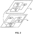
- FIG. 2 is a block diagram of one embodiment of a first die having a single sensor and a second die having multiple sensors.
- the example of FIG. 2 illustrates two dice that may be stacked so that the heat from one die may transfer to the other die.
- the example of FIG. 2 illustrates only two dice, but the concepts illustrated are applicable to any number of stacked dice.
- Die 220 may include any type of circuitry, for example, DRAM arrays, or other memory structures 235.
- Die 220 includes thermal sensor 240 coupled with management logic 230.
- management logic 230 may operate to read temperature information from thermal sensor 240 and may use that temperature information to modify behavior or operation of memory array 235.
- the refresh rate of memory array 235 may be adjusted by management logic 230 based on information from thermal sensor 240.
- Die 250 may include logic circuitry, for example, a processor core, a graphics processor, a system on a chip (SoC), or other logic 275. Die 250 may have multiple types of circuits, for example, a processor core, a cache memory, a transceiver, etc. Because die 250 may have circuits with irregular thermal gradients, die 250 may have multiple thermal sensors (e.g., 260, 265), one of which is to be aligned with thermal sensor 240.
- SoC system on a chip
- thermal sensor 240 may be placed in a predetermined location on die 220 that is known to designers and/or manufacturers of die 250.
- Thermal sensor 260 is positioned so that when die 220 is stacked on die 250, thermal sensors 240 and 260 will be aligned or close enough spatially that temperature information from thermal sensor 260 may be utilized with temperature information from thermal sensor 240.
- Control circuit 270 is coupled with thermal sensors 260 and 265 to collect temperature information. In one embodiment, control circuit 270 determines a temperature difference between thermal sensor 265 and thermal sensor 260. Control circuit 270 may transmit this difference (or information indicating a difference range), to management logic 230. In one embodiment, a bit in a register in management logic 230 is set to indicate a temperature difference (e.g., 0 indicates 0-10 degree difference, 1 indicates a 10+ degree difference). In another embodiment, more bits may be used to provide a more granular range, or an actual temperature difference may be transmitted.
- Management logic 230 uses the temperature difference information from control circuit 270 with temperature information from thermal sensor 240 to manage operation of memory array 235. In one embodiment, management logic 230 controls a refresh rate for memory array 235. Management logic 230 may combine the temperature difference information with the temperature information from thermal sensor 240 to determine an operational temperature value that is used for management of memory array 235. For example, if the temperature difference indicates a higher temperature, management logic 230 may increase the refresh rate for memory array 235.
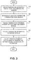
- FIG. 3 is a flow diagram of one embodiment of a technique to operate a memory array using temperature difference information. The operations described with respect to FIG. 3 may be performed by control and/or management circuitry spread across one or more dice.
- FIG. 3 The operation of FIG. 3 is applicable to a configuration of multiple dice that are physically in contact with one another so that thermal transfer may occur.
- at least one thermal sensor on the lower die is aligned with at least one sensor on the upper die.
- the lower die contains a logic circuit, for example, a processor core or a system on a chip.
- the upper die may contain a memory structure, for example, a DRAM.
- the logic circuit is on the upper die and the memory module is on the lower die.
- Temperature information from two or more thermal sensors is collected on the logic die, 310.
- the logic die may have any number of thermal sensors and, one or more circuits on the logic die may manage operation of the logic die by utilizing the temperature information collected from the multiple thermal sensors.
- Temperature difference information is determined for at least one pair of thermal sensors on the logic die, 320.
- at least one of the thermal sensors for which a temperature difference is determined is aligned with a corresponding thermal sensor on the memory module die.
- the temperature difference information is transmitted between the logic die and the memory die, 330.
- the temperature difference may be communicated by one or more bits that indicate temperature differential ranges, or a number indicating an actual temperature difference may be transmitted.
- a 0 may indicate a temperature difference in a first range (e.g., 0-5 degrees, 0-10 degrees, 0-12 degrees) and a 1 may indicate a temperature difference in a second range (e.g., >5 degrees, >10 degrees, >12 degrees).
- a 00 may indicate a first range (e.g., 0-5 degrees, 0-7 degrees, 0-10 degrees)
- a 01 may indicate a second range (e.g., 6-10 degrees, 8-15 degrees, 11-20 degrees)
- a 10 may indicate a third range (e.g., 11-15 degrees, 16-20 degrees, 21-25 degrees)
- a 11 may indicate a fourth range (e.g., >15 degrees, >20 degrees, >25 degrees).
- Other embodiments with different numbers of bits may be similarly supported.
- Temperature information is gathered for the memory module, 340.
- the memory module has only one thermal sensor that is aligned with one of the thermal sensors of the logic die.
- the memory module may have multiple thermal sensors.
- the memory module may have management (or other control) circuitry that utilizes temperature information to manage operation of the memory module.
- the refresh rate for the memory array is determined based, at least in part, on the operating temperature of the memory module.
- the management circuitry utilizes the temperature information from the memory module thermal sensor and the temperature difference information to adjust, if necessary, the operational parameters of the memory module, 350.
- the refresh rate of the memory module may be determined based on the measured temperature as adjusted by the temperature difference information. Other operational parameters may also be adjusted.
- temperature difference information may be shared between the dice, which will allow the respective control circuits to have more accurate information upon which to base operational parameters.
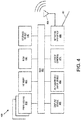
- FIG. 4 is a block diagram of one embodiment of an electronic system.
- the electronic system illustrated in FIG. 4 is intended to represent a range of electronic systems (either wired or wireless) including, for example, desktop computer systems, laptop computer systems, cellular telephones, personal digital assistants (PDAs) including cellular-enabled PDAs, set top boxes.
- Alternative electronic systems may include more, fewer and/or different components.
- One or more of the components illustrated in FIG. 4 may be on dice that are in physical contact as described above.
- processors 410 and one or more DRAM modules that are part of memory 420 may be arranged as described above.
- Other components may be similarly arranged.
- Electronic system 400 includes bus 405 or other communication device to communicate information, and processor 410 coupled to bus 405 that may process information. While electronic system 400 is illustrated with a single processor, electronic system 400 may include multiple processors and/or co-processors. Electronic system 400 further may include random access memory (RAM) or other dynamic storage device 420 (referred to as main memory), coupled to bus 405 and may store information and instructions that may be executed by processor 410. Main memory 420 may also be used to store temporary variables or other intermediate information during execution of instructions by processor 410.
- RAM random access memory
- main memory main memory
- Electronic system 400 may also include read only memory (ROM) and/or other static storage device 430 coupled to bus 405 that may store static information and instructions for processor 410.
- Data storage device 440 may be coupled to bus 405 to store information and instructions.
- Data storage device 440 such as a magnetic disk or optical disc and corresponding drive may be coupled to electronic system 400.
- Electronic system 400 may also be coupled via bus 405 to display device 450, such as a cathode ray tube (CRT) or liquid crystal display (LCD), to display information to a user.
- display device 450 such as a cathode ray tube (CRT) or liquid crystal display (LCD)
- Alphanumeric input device 460 may be coupled to bus 405 to communicate information and command selections to processor 410.
- cursor control 470 such as a mouse, a trackball, or cursor direction keys to communicate direction information and command selections to processor 410 and to control cursor movement on display 450.
- Electronic system 400 further may include network interface(s) 480 to provide access to a network, such as a local area network.
- Network interface(s) 480 may include, for example, a wireless network interface having antenna 485, which may represent one or more antenna(e).
- Network interface(s) 480 may also include, for example, a wired network interface to communicate with remote devices via network cable 487, which may be, for example, an Ethernet cable, a coaxial cable, a fiber optic cable, a serial cable, or a parallel cable.
- network interface(s) 480 may provide access to a local area network, for example, by conforming to IEEE 802.1 1b and/or IEEE 802.11g standards, and/or the wireless network interface may provide access to a personal area network, for example, by conforming to Bluetooth standards. Other wireless network interfaces and/or protocols can also be supported.
- IEEE 802.11b corresponds to IEEE Std. 802.11b-1999 entitled “Local and Metropolitan Area Networks, Part 11: Wireless LAN Medium Access Control (MAC) and Physical Layer (PHY) Specifications: Higher-Speed Physical Layer Extension in the 2.4 GHz Band," approved Sep. 16, 1999 as well as related documents.
- IEEE 802.11g corresponds to IEEE Std. 802.11g-2003 entitled “Local and Metropolitan Area Networks, Part 11: Wireless LAN Medium Access Control (MAC) and Physical Layer (PHY) Specifications, Amendment 4: Further Higher Rate Extension in the 2.4 GHz Band," approved Jun. 27, 2003 as well as related documents.
- Bluetooth protocols are described in "Specification of the Bluetooth System: Core, Version 1.1,” published Feb. 22, 2001 by the Bluetooth Special Interest Group, Inc. Associated as well as previous or subsequent versions of the Bluetooth standard may also be supported.
- network interface(s) 480 may provide wireless communications using, for example, Time Division, Multiple Access (TDMA) protocols, Global System for Mobile Communications (GSM) protocols, Code Division, Multiple Access (CDMA) protocols, and/or any other type of wireless communications protocol.
- TDMA Time Division, Multiple Access
- GSM Global System for Mobile Communications
- CDMA Code Division, Multiple Access
Claims (11)
- Appareil, comprenant :
une microplaquette à semi-conducteur (250) incluant :un premier capteur thermique (260) et un second capteur thermique (265), les premier et second capteurs thermiques étant utilisables pour détecter un gradient thermique pour la microplaquette à semi-conducteur (250), etune circuiterie logique (270) utilisable pour fournir un bit de décalage thermique à un emplacement de stockage pour le bit de décalage thermique d'un registre de mode d'une microplaquette de mémoire (220) en réponse à la détection d'un changement du gradient thermique pour la microplaquette à semi-conducteur (250), la microplaquette de mémoire incluant une mémoire vive dynamique, DRAM (235) ;dans lequel le bit de décalage thermique est destiné à diriger une logique d'autorafraîchissement compensé en température, TCSR, de la microplaquette de mémoire pour modifier une fréquence d'autorafraîchissement de la DRAM ;dans lequel le premier capteur thermique est aligné avec un capteur thermique de mémoire (240), ou est à proximité étroite de ce dernier, de la microplaquette de mémoire, et dans lequel le second capteur thermique de la microplaquette à semi-conducteur est situé à un point chaud de la microplaquette à semi-conducteur. - Appareil selon la revendication 1, dans lequel un emplacement du capteur thermique de mémoire par rapport au premier capteur thermique est destiné à permettre l'utilisation d'informations de température à partir du premier capteur thermique avec des informations de température à partir du capteur thermique de mémoire.
- Appareil selon la revendication 1, dans lequel la microplaquette à semi-conducteur est physiquement connectée à la microplaquette de mémoire pour fournir un couplage thermique de la microplaquette à semi-conducteur à la microplaquette de mémoire.
- Appareil selon la revendication 1, dans lequel une valeur du bit de décalage thermique est destinée à représenter une plage de température pour le gradient thermique.
- Appareil selon la revendication 1, dans lequel la microplaquette à semi-conducteur comprend un coeur de processeur ou processeur graphique (275).
- Appareil selon la revendication 1, dans lequel la microplaquette à semi-conducteur comprend un système sur puce (SoC).
- Appareil selon la revendication 1, comprenant en outre :un ou plusieurs processeurs (410) couplés en communication à la circuiterie logique ;une interface de réseau (480) couplée en communication à au moins l'un du ou des processeurs ; etun dispositif d'affichage (450) couplé en communication à au moins l'un du ou des processeurs.
- Procédé, comprenant :la détection d'un gradient thermique pour une microplaquette à semi-conducteur avec un premier capteur thermique et un second capteur thermique de la microplaquette à semi-conducteur ;la génération, par une circuiterie logique de la microplaquette à semi-conducteur, d'un bit de décalage thermique en réponse à la détection d'un changement du gradient thermique pour la microplaquette à semi-conducteur ; etla transmission du bit de décalage thermique pour le stockage dans un emplacement de stockage d'un registre de mode d'une microplaquette de mémoire, la microplaquette de mémoire incluant une mémoire vive dynamique, DRAM ;dans lequel le bit de décalage thermique est destiné à diriger une logique d'autorafraîchissement compensé en température, TCSR, de la microplaquette de mémoire pour modifier une fréquence d'autorafraîchissement de la DRAM ;dans lequel le premier capteur thermique est aligné avec un capteur thermique de mémoire, ou à proximité étroite de ce dernier, de la microplaquette de mémoire, et le second capteur thermique est situé à un point chaud de la microplaquette à semi-conducteur.
- Procédé selon la revendication 8, dans lequel un emplacement du capteur thermique de mémoire par rapport au premier capteur thermique est destiné à permettre l'utilisation d'informations de température à partir du premier capteur thermique avec des informations de température à partir du capteur thermique de mémoire.
- Procédé selon la revendication 8, dans lequel la microplaquette à semi-conducteur est physiquement connectée à la microplaquette de mémoire pour fournir un couplage thermique de la microplaquette à semi-conducteur à la microplaquette de mémoire.
- Procédé selon la revendication 8, dans lequel une valeur du bit de décalage thermique est destinée à représenter une plage de température pour le gradient thermique.
Applications Claiming Priority (2)
| Application Number | Priority Date | Filing Date | Title |
|---|---|---|---|
| US13/077,661 US9490003B2 (en) | 2011-03-31 | 2011-03-31 | Induced thermal gradients |
| EP12763926.8A EP2695192B1 (fr) | 2011-03-31 | 2012-02-08 | Gradients thermiques induits |
Related Parent Applications (2)
| Application Number | Title | Priority Date | Filing Date |
|---|---|---|---|
| EP12763926.8A Division EP2695192B1 (fr) | 2011-03-31 | 2012-02-08 | Gradients thermiques induits |
| EP12763926.8A Division-Into EP2695192B1 (fr) | 2011-03-31 | 2012-02-08 | Gradients thermiques induits |
Publications (2)
| Publication Number | Publication Date |
|---|---|
| EP2996014A1 EP2996014A1 (fr) | 2016-03-16 |
| EP2996014B1 true EP2996014B1 (fr) | 2018-05-16 |
Family
ID=46926406
Family Applications (2)
| Application Number | Title | Priority Date | Filing Date |
|---|---|---|---|
| EP12763926.8A Active EP2695192B1 (fr) | 2011-03-31 | 2012-02-08 | Gradients thermiques induits |
| EP15187070.6A Active EP2996014B1 (fr) | 2011-03-31 | 2012-02-08 | Gradients thermiques induits |
Family Applications Before (1)
| Application Number | Title | Priority Date | Filing Date |
|---|---|---|---|
| EP12763926.8A Active EP2695192B1 (fr) | 2011-03-31 | 2012-02-08 | Gradients thermiques induits |
Country Status (6)
| Country | Link |
|---|---|
| US (2) | US9490003B2 (fr) |
| EP (2) | EP2695192B1 (fr) |
| KR (2) | KR101732840B1 (fr) |
| CN (2) | CN103460382B (fr) |
| TW (2) | TWI537719B (fr) |
| WO (1) | WO2012134637A1 (fr) |
Families Citing this family (21)
| Publication number | Priority date | Publication date | Assignee | Title |
|---|---|---|---|---|
| TWI430094B (zh) * | 2011-09-22 | 2014-03-11 | Phison Electronics Corp | 記憶體儲存裝置、記憶體控制器與溫度管理方法 |
| US10156512B2 (en) * | 2013-03-01 | 2018-12-18 | Futurewei Technologies, Inc. | System and method for measuring thermal reliability of multi-chip modules |
| KR102063817B1 (ko) * | 2013-03-04 | 2020-01-08 | 삼성전자주식회사 | 반도체 패키지를 포함하는 반도체 장치의 표면 온도 제어 방법 |
| US9285278B2 (en) * | 2013-05-09 | 2016-03-15 | Apple Inc. | System and methods for thermal control using sensors on die |
| US9390785B2 (en) | 2014-03-27 | 2016-07-12 | Intel Corporation | Method, apparatus and system for determining a write recovery time of a memory based on temperature |
| JP6425462B2 (ja) * | 2014-08-27 | 2018-11-21 | ルネサスエレクトロニクス株式会社 | 半導体装置 |
| US9996110B2 (en) * | 2014-12-24 | 2018-06-12 | Intel Corporation | Direct attach dock cooling leveraging maximum silicon junction temperature control |
| KR102373543B1 (ko) | 2015-04-08 | 2022-03-11 | 삼성전자주식회사 | 멀티칩 패키지에서 온도 편차를 이용하여 동작 제어하는 방법 및 장치 |
| US10248173B2 (en) * | 2016-03-31 | 2019-04-02 | Intel Corporation | Determining thermal margins in a multi-die processor |
| KR102571497B1 (ko) | 2016-05-10 | 2023-08-29 | 삼성전자주식회사 | 멀티 스택 칩 패키지를 포함하는 데이터 저장 장치 및 그것의 동작 방법 |
| US9653144B1 (en) * | 2016-06-28 | 2017-05-16 | Intel Corporation | Apparatuses, methods, and systems for package on package memory refresh and self-refresh rate management |
| KR102656205B1 (ko) * | 2016-10-25 | 2024-04-11 | 에스케이하이닉스 주식회사 | 온도 제어 장치, 이를 포함하는 반도체 장치 및 반도체 장치의 제어 방법 |
| EP3340187A1 (fr) * | 2016-12-26 | 2018-06-27 | Thomson Licensing | Dispositif et procédé de génération de contenus virtuels dynamiques en réalité mixte |
| KR20180099266A (ko) | 2017-02-28 | 2018-09-05 | 삼성전자주식회사 | 데이터 저장 장치, 그의 동작 방법 및 그를 포함하는 전자 시스템 |
| KR20190036893A (ko) | 2017-09-28 | 2019-04-05 | 삼성전자주식회사 | 메모리 장치 및 그것의 제어 방법 |
| FR3075392B1 (fr) * | 2017-12-14 | 2020-09-11 | Thales Sa | Surveillance d'un defaut dans un equipement electrique |
| US10528288B2 (en) | 2017-12-20 | 2020-01-07 | International Business Machines Corporation | Three-dimensional stacked memory access optimization |
| US10497423B1 (en) | 2018-05-14 | 2019-12-03 | Nanya Technology Corporation | Frequency-adjusting circuit, electronic memory, and method for determining a refresh frequency for a plurality of dram chips |
| US10928439B2 (en) * | 2018-10-03 | 2021-02-23 | Semiconductor Components Industries, Llc | Thermal gradient correction of a current monitor signal |
| US11321008B2 (en) * | 2018-11-15 | 2022-05-03 | Micron Technology, Inc. | Temperature-based memory management |
| CN113936733A (zh) * | 2021-10-15 | 2022-01-14 | 西安紫光国芯半导体有限公司 | 三维集成电路晶圆的测试方法、测试装置和三维集成电路 |
Family Cites Families (78)
| Publication number | Priority date | Publication date | Assignee | Title |
|---|---|---|---|---|
| US5502838A (en) * | 1994-04-28 | 1996-03-26 | Consilium Overseas Limited | Temperature management for integrated circuits |
| US5902044A (en) * | 1997-06-27 | 1999-05-11 | International Business Machines Corporation | Integrated hot spot detector for design, analysis, and control |
| US6789037B2 (en) * | 1999-03-30 | 2004-09-07 | Intel Corporation | Methods and apparatus for thermal management of an integrated circuit die |
| US6169442B1 (en) * | 1999-04-13 | 2001-01-02 | Analog Devices, Inc. | IC monitoring chip and a method for monitoring temperature of a component in a computer |
| US6488405B1 (en) * | 2000-03-08 | 2002-12-03 | Advanced Micro Devices, Inc. | Flip chip defect analysis using liquid crystal |
| US6513723B1 (en) * | 2000-09-28 | 2003-02-04 | Emerson Electric Co. | Method and apparatus for automatically transmitting temperature information to a thermostat |
| US6662136B2 (en) | 2001-04-10 | 2003-12-09 | International Business Machines Corporation | Digital temperature sensor (DTS) system to monitor temperature in a memory subsystem |
| US6557072B2 (en) | 2001-05-10 | 2003-04-29 | Palm, Inc. | Predictive temperature compensation for memory devices systems and method |
| US20030158683A1 (en) | 2002-02-19 | 2003-08-21 | Claude Gauthier | Temperature calibration using on-chip electrical fuses |
| US6908227B2 (en) * | 2002-08-23 | 2005-06-21 | Intel Corporation | Apparatus for thermal management of multiple core microprocessors |
| US6781908B1 (en) | 2003-02-19 | 2004-08-24 | Freescale Semiconductor, Inc. | Memory having variable refresh control and method therefor |
| KR100577560B1 (ko) * | 2003-12-23 | 2006-05-08 | 삼성전자주식회사 | 온도감지 데이터에 응답하는 내부회로를 갖는 반도체메모리장치 |
| US7583551B2 (en) | 2004-03-10 | 2009-09-01 | Micron Technology, Inc. | Power management control and controlling memory refresh operations |
| NO20042771D0 (no) | 2004-06-30 | 2004-06-30 | Thin Film Electronics Asa | Optimering av driftstemperatur i et ferroelektrisk eller elektret minne |
| US7099735B2 (en) | 2004-06-30 | 2006-08-29 | Intel Corporation | Method and apparatus to control the temperature of a memory device |
| US8122187B2 (en) | 2004-07-02 | 2012-02-21 | Qualcomm Incorporated | Refreshing dynamic volatile memory |
| US7347621B2 (en) * | 2004-07-16 | 2008-03-25 | International Business Machines Corporation | Method and system for real-time estimation and prediction of the thermal state of a microprocessor unit |
| US7523285B2 (en) * | 2004-08-20 | 2009-04-21 | Intel Corporation | Thermal memory control |
| JP4479453B2 (ja) | 2004-10-01 | 2010-06-09 | 三菱電機株式会社 | 電力半導体装置 |
| KR100611505B1 (ko) | 2004-12-17 | 2006-08-11 | 삼성전자주식회사 | 동적 온도 모니터링이 가능한 메모리 모듈 및 메모리모듈의 동작 방법 |
| US7413342B2 (en) * | 2005-02-22 | 2008-08-19 | Micron Technology, Inc. | DRAM temperature measurement system |
| US7400945B2 (en) | 2005-03-23 | 2008-07-15 | Intel Corporation | On-die temperature monitoring in semiconductor devices to limit activity overload |
| US7260007B2 (en) * | 2005-03-30 | 2007-08-21 | Intel Corporation | Temperature determination and communication for multiple devices of a memory module |
| US20060236027A1 (en) | 2005-03-30 | 2006-10-19 | Sandeep Jain | Variable memory array self-refresh rates in suspend and standby modes |
| US9171585B2 (en) * | 2005-06-24 | 2015-10-27 | Google Inc. | Configurable memory circuit system and method |
| US7535020B2 (en) * | 2005-06-28 | 2009-05-19 | Kabushiki Kaisha Toshiba | Systems and methods for thermal sensing |
| US8330476B2 (en) | 2005-08-31 | 2012-12-11 | Ati Technologies Ulc | Dynamic voltage and power management by temperature monitoring |
| DE102005056907B3 (de) * | 2005-11-29 | 2007-08-16 | Infineon Technologies Ag | 3-dimensionales Mehrchip-Modul |
| US7441949B2 (en) | 2005-12-16 | 2008-10-28 | Micron Technology, Inc. | System and method for providing temperature data from a memory device having a temperature sensor |
| US7765825B2 (en) | 2005-12-16 | 2010-08-03 | Intel Corporation | Apparatus and method for thermal management of a memory device |
| KR100725458B1 (ko) * | 2005-12-23 | 2007-06-07 | 삼성전자주식회사 | 온도 보상 셀프 리프레시 신호를 공유하는 멀티 칩 패키지 |
| US7590473B2 (en) | 2006-02-16 | 2009-09-15 | Intel Corporation | Thermal management using an on-die thermal sensor |
| US7510323B2 (en) * | 2006-03-14 | 2009-03-31 | International Business Machines Corporation | Multi-layered thermal sensor for integrated circuits and other layered structures |
| CN100390750C (zh) | 2006-04-04 | 2008-05-28 | 威盛电子股份有限公司 | 存储器刷新速度的控制装置及方法 |
| JP5065618B2 (ja) * | 2006-05-16 | 2012-11-07 | 株式会社日立製作所 | メモリモジュール |
| US7532021B2 (en) * | 2006-06-06 | 2009-05-12 | Advanced Inquiry Systems, Inc. | Apparatus for translated wafer stand-in tester |
| US7535110B2 (en) * | 2006-06-15 | 2009-05-19 | Marvell World Trade Ltd. | Stack die packages |
| US8118483B2 (en) * | 2006-06-21 | 2012-02-21 | Intel Corporation | Thermal sensor having toggle control |
| US20080005591A1 (en) * | 2006-06-28 | 2008-01-03 | Trautman Mark A | Method, system, and apparatus for dynamic thermal management |
| US7549795B2 (en) * | 2006-06-30 | 2009-06-23 | Intel Corporation | Analog thermal sensor array |
| US8272781B2 (en) | 2006-08-01 | 2012-09-25 | Intel Corporation | Dynamic power control of a memory device thermal sensor |
| US8762097B2 (en) | 2006-08-04 | 2014-06-24 | Apple Inc. | Method and apparatus for a thermal control system based on virtual temperature sensor |
| KR100832029B1 (ko) | 2006-09-28 | 2008-05-26 | 주식회사 하이닉스반도체 | 온도 정보 출력 장치 및 그를 갖는 반도체 소자 |
| US8122265B2 (en) * | 2006-12-29 | 2012-02-21 | Intel Corporation | Power management using adaptive thermal throttling |
| KR100834403B1 (ko) * | 2007-01-03 | 2008-06-04 | 주식회사 하이닉스반도체 | 안정적인 셀프리프레쉬 동작을 수행하는 메모리장치 및셀프리프레쉬주기 제어신호 생성방법 |
| KR101257912B1 (ko) * | 2007-02-14 | 2013-04-24 | 삼성전자주식회사 | 반도체 메모리 장치와 이 장치의 단자 배치 방법, 및 이장치를 구비한 메모리 모듈과 이 모듈의 기판의 단자 및라인 배치 방법 |
| US20080239852A1 (en) | 2007-03-28 | 2008-10-02 | Reza Jazayeri | Test feature to improve DRAM charge retention yield |
| KR100949877B1 (ko) | 2007-04-10 | 2010-03-25 | 주식회사 하이닉스반도체 | 반도체 패키지 |
| JP5669338B2 (ja) * | 2007-04-26 | 2015-02-12 | 株式会社日立製作所 | 半導体装置 |
| US7621671B2 (en) * | 2007-05-16 | 2009-11-24 | Infineon Technologies Ag | Method and apparatus for thermal protection in an integrated circuit |
| US7771115B2 (en) | 2007-08-16 | 2010-08-10 | Micron Technology, Inc. | Temperature sensor circuit, device, system, and method |
| US7768857B2 (en) | 2007-12-03 | 2010-08-03 | Qimonda Ag | Method of refreshing data in a storage location based on heat dissipation level and system thereof |
| FI122943B (fi) * | 2007-12-04 | 2012-09-14 | Sensire Oy | Laite, menetelmä ja järjestelmä tiedon välittämiseksi RFID-laitteilta |
| USRE45029E1 (en) * | 2007-12-24 | 2014-07-22 | Uniforce Tech Limited Liability Company | Thermal sensors for stacked dies |
| KR101007988B1 (ko) | 2008-01-02 | 2011-01-14 | 주식회사 하이닉스반도체 | 온도정보 출력회로 및 이를 이용한 멀티칩패키지 |
| US8209493B2 (en) * | 2008-03-26 | 2012-06-26 | Intel Corporation | Systems and methods for scheduling memory requests during memory throttling |
| US20090256622A1 (en) * | 2008-04-11 | 2009-10-15 | Nortel Networks Limited | Soft thermal failure in a high capacity transmission system |
| US7923829B2 (en) * | 2008-05-06 | 2011-04-12 | Mediatek Inc. | Bonding pad sharing method applied to multi-chip module and apparatus thereof |
| KR101559549B1 (ko) * | 2008-12-08 | 2015-10-13 | 삼성전자주식회사 | 모바일 SoC 및 모바일 단말기 |
| KR101596281B1 (ko) | 2008-12-19 | 2016-02-22 | 삼성전자 주식회사 | 온도 관련 공유 제어회로를 갖는 반도체 메모리 장치 |
| US7929368B2 (en) | 2008-12-30 | 2011-04-19 | Micron Technology, Inc. | Variable memory refresh devices and methods |
| US7984250B2 (en) | 2008-12-31 | 2011-07-19 | Intel Corporation | Dynamic updating of thresholds in accordance with operating conditons |
| US8032804B2 (en) * | 2009-01-12 | 2011-10-04 | Micron Technology, Inc. | Systems and methods for monitoring a memory system |
| US8624527B1 (en) | 2009-03-27 | 2014-01-07 | Oree, Inc. | Independently controllable illumination device |
| US8527113B2 (en) | 2009-08-07 | 2013-09-03 | Irobot Corporation | Remote vehicle |
| US20110093132A1 (en) | 2009-10-19 | 2011-04-21 | Apple Inc. | Platform-independent thermal management of components in electronic devices |
| US8796863B2 (en) * | 2010-02-09 | 2014-08-05 | Samsung Electronics Co., Ltd. | Semiconductor memory devices and semiconductor packages |
| KR101817156B1 (ko) * | 2010-12-28 | 2018-01-10 | 삼성전자 주식회사 | 관통 전극을 갖는 적층 구조의 반도체 장치, 반도체 메모리 장치, 반도체 메모리 시스템 및 그 동작방법 |
| CN103999162A (zh) * | 2011-12-23 | 2014-08-20 | 英特尔公司 | 用于堆叠存储器架构的自修复逻辑 |
| WO2013095674A1 (fr) | 2011-12-23 | 2013-06-27 | Intel Corporation | Opérations de mémoire utilisant des données de capteur de température de système |
| KR101642208B1 (ko) | 2011-12-23 | 2016-07-22 | 인텔 코포레이션 | 동적 메모리 성능 스로틀링 |
| DE112011106009T5 (de) | 2011-12-23 | 2014-12-18 | Intel Corp. | Getrennte Mikrokanal-Spannungsdomänen in Stapelspeicherarchitektur |
| DE112011106076B4 (de) | 2011-12-28 | 2020-01-23 | Intel Corp. | Generischer Adressen-Scrambler für Speicherschaltungs-Testengine |
| US8645777B2 (en) | 2011-12-29 | 2014-02-04 | Intel Corporation | Boundary scan chain for stacked memory |
| US8892269B2 (en) | 2012-03-30 | 2014-11-18 | Intel Corporation | Power down and quick start of thermal sensor |
| WO2014041648A1 (fr) * | 2012-09-12 | 2014-03-20 | ルネサスエレクトロニクス株式会社 | Dispositif à semi-conducteur |
| US9016939B2 (en) * | 2012-10-01 | 2015-04-28 | Taiwan Semiconductor Manufacturing Co., Ltd. | Thermal sensor with second-order temperature curvature correction |
| JP6101047B2 (ja) * | 2012-11-07 | 2017-03-22 | キヤノン株式会社 | 情報処理装置及びその制御方法、並びにプログラム |
-
2011
- 2011-03-31 US US13/077,661 patent/US9490003B2/en active Active
-
2012
- 2012-02-08 KR KR1020157031435A patent/KR101732840B1/ko active IP Right Grant
- 2012-02-08 EP EP12763926.8A patent/EP2695192B1/fr active Active
- 2012-02-08 CN CN201280016742.2A patent/CN103460382B/zh active Active
- 2012-02-08 KR KR1020137025329A patent/KR101594663B1/ko active IP Right Grant
- 2012-02-08 CN CN201510627479.6A patent/CN105244053B/zh active Active
- 2012-02-08 EP EP15187070.6A patent/EP2996014B1/fr active Active
- 2012-02-08 WO PCT/US2012/024340 patent/WO2012134637A1/fr active Application Filing
- 2012-02-10 TW TW101104389A patent/TWI537719B/zh active
- 2012-02-10 TW TW104137715A patent/TWI567546B/zh active
-
2015
- 2015-08-28 US US14/838,994 patent/US20160055901A1/en not_active Abandoned
Non-Patent Citations (1)
| Title |
|---|
| None * |
Also Published As
| Publication number | Publication date |
|---|---|
| CN103460382A (zh) | 2013-12-18 |
| US9490003B2 (en) | 2016-11-08 |
| KR101594663B1 (ko) | 2016-02-16 |
| KR20130133001A (ko) | 2013-12-05 |
| EP2695192A1 (fr) | 2014-02-12 |
| TWI567546B (zh) | 2017-01-21 |
| EP2996014A1 (fr) | 2016-03-16 |
| CN105244053A (zh) | 2016-01-13 |
| US20160055901A1 (en) | 2016-02-25 |
| TW201610668A (zh) | 2016-03-16 |
| WO2012134637A1 (fr) | 2012-10-04 |
| TWI537719B (zh) | 2016-06-11 |
| US20120249218A1 (en) | 2012-10-04 |
| KR101732840B1 (ko) | 2017-05-04 |
| EP2695192A4 (fr) | 2014-12-10 |
| KR20150132589A (ko) | 2015-11-25 |
| TW201250467A (en) | 2012-12-16 |
| CN103460382B (zh) | 2016-08-17 |
| CN105244053B (zh) | 2018-07-10 |
| EP2695192B1 (fr) | 2017-05-03 |
Similar Documents
| Publication | Publication Date | Title |
|---|---|---|
| EP2996014B1 (fr) | Gradients thermiques induits | |
| US10514305B2 (en) | Induced thermal gradients | |
| US10199085B2 (en) | Semiconductor device | |
| US10224078B2 (en) | Semiconductor device and refresh rate control method of semiconductor device based on measured temperature | |
| CN101133403B (zh) | 使用存储器总线实现存储设备通信的方法和装置 | |
| US9396787B2 (en) | Memory operations using system thermal sensor data | |
| KR100954733B1 (ko) | 메모리 모듈 및 이를 포함하는 장치와, 메모리 모듈의 구성요소들의 동작 온도를 검출하는 방법 | |
| US9116050B2 (en) | Sensor-based thermal specification enabling a real-time metric for compliance | |
| KR102254098B1 (ko) | 온도를 센싱할 수 있는 반도체 칩, 및 상기 반도체 칩을 포함하는 반도체 시스템 | |
| JP2005032428A (ja) | メモリのリフレッシュ周期を制御するメモリコントローラおよびリフレッシュ周期制御方法 | |
| KR102656205B1 (ko) | 온도 제어 장치, 이를 포함하는 반도체 장치 및 반도체 장치의 제어 방법 | |
| US20190207842A1 (en) | System including master device and slave device, and operation method of the system |
Legal Events
| Date | Code | Title | Description |
|---|---|---|---|
| PUAI | Public reference made under article 153(3) epc to a published international application that has entered the european phase |
Free format text: ORIGINAL CODE: 0009012 |
|
| 17P | Request for examination filed |
Effective date: 20150928 |
|
| AC | Divisional application: reference to earlier application |
Ref document number: 2695192 Country of ref document: EP Kind code of ref document: P |
|
| AK | Designated contracting states |
Kind code of ref document: A1 Designated state(s): AL AT BE BG CH CY CZ DE DK EE ES FI FR GB GR HR HU IE IS IT LI LT LU LV MC MK MT NL NO PL PT RO RS SE SI SK SM TR |
|
| GRAP | Despatch of communication of intention to grant a patent |
Free format text: ORIGINAL CODE: EPIDOSNIGR1 |
|
| STAA | Information on the status of an ep patent application or granted ep patent |
Free format text: STATUS: GRANT OF PATENT IS INTENDED |
|
| INTG | Intention to grant announced |
Effective date: 20171123 |
|
| GRAS | Grant fee paid |
Free format text: ORIGINAL CODE: EPIDOSNIGR3 |
|
| GRAA | (expected) grant |
Free format text: ORIGINAL CODE: 0009210 |
|
| STAA | Information on the status of an ep patent application or granted ep patent |
Free format text: STATUS: THE PATENT HAS BEEN GRANTED |
|
| AC | Divisional application: reference to earlier application |
Ref document number: 2695192 Country of ref document: EP Kind code of ref document: P |
|
| AK | Designated contracting states |
Kind code of ref document: B1 Designated state(s): AL AT BE BG CH CY CZ DE DK EE ES FI FR GB GR HR HU IE IS IT LI LT LU LV MC MK MT NL NO PL PT RO RS SE SI SK SM TR |
|
| REG | Reference to a national code |
Ref country code: GB Ref legal event code: FG4D |
|
| REG | Reference to a national code |
Ref country code: CH Ref legal event code: EP |
|
| REG | Reference to a national code |
Ref country code: IE Ref legal event code: FG4D |
|
| REG | Reference to a national code |
Ref country code: DE Ref legal event code: R096 Ref document number: 602012046522 Country of ref document: DE |
|
| REG | Reference to a national code |
Ref country code: AT Ref legal event code: REF Ref document number: 1000134 Country of ref document: AT Kind code of ref document: T Effective date: 20180615 |
|
| REG | Reference to a national code |
Ref country code: NL Ref legal event code: FP |
|
| REG | Reference to a national code |
Ref country code: LT Ref legal event code: MG4D |
|
| PG25 | Lapsed in a contracting state [announced via postgrant information from national office to epo] |
Ref country code: SE Free format text: LAPSE BECAUSE OF FAILURE TO SUBMIT A TRANSLATION OF THE DESCRIPTION OR TO PAY THE FEE WITHIN THE PRESCRIBED TIME-LIMIT Effective date: 20180516 Ref country code: LT Free format text: LAPSE BECAUSE OF FAILURE TO SUBMIT A TRANSLATION OF THE DESCRIPTION OR TO PAY THE FEE WITHIN THE PRESCRIBED TIME-LIMIT Effective date: 20180516 Ref country code: ES Free format text: LAPSE BECAUSE OF FAILURE TO SUBMIT A TRANSLATION OF THE DESCRIPTION OR TO PAY THE FEE WITHIN THE PRESCRIBED TIME-LIMIT Effective date: 20180516 Ref country code: BG Free format text: LAPSE BECAUSE OF FAILURE TO SUBMIT A TRANSLATION OF THE DESCRIPTION OR TO PAY THE FEE WITHIN THE PRESCRIBED TIME-LIMIT Effective date: 20180816 Ref country code: NO Free format text: LAPSE BECAUSE OF FAILURE TO SUBMIT A TRANSLATION OF THE DESCRIPTION OR TO PAY THE FEE WITHIN THE PRESCRIBED TIME-LIMIT Effective date: 20180816 Ref country code: FI Free format text: LAPSE BECAUSE OF FAILURE TO SUBMIT A TRANSLATION OF THE DESCRIPTION OR TO PAY THE FEE WITHIN THE PRESCRIBED TIME-LIMIT Effective date: 20180516 |
|
| PG25 | Lapsed in a contracting state [announced via postgrant information from national office to epo] |
Ref country code: LV Free format text: LAPSE BECAUSE OF FAILURE TO SUBMIT A TRANSLATION OF THE DESCRIPTION OR TO PAY THE FEE WITHIN THE PRESCRIBED TIME-LIMIT Effective date: 20180516 Ref country code: RS Free format text: LAPSE BECAUSE OF FAILURE TO SUBMIT A TRANSLATION OF THE DESCRIPTION OR TO PAY THE FEE WITHIN THE PRESCRIBED TIME-LIMIT Effective date: 20180516 Ref country code: HR Free format text: LAPSE BECAUSE OF FAILURE TO SUBMIT A TRANSLATION OF THE DESCRIPTION OR TO PAY THE FEE WITHIN THE PRESCRIBED TIME-LIMIT Effective date: 20180516 Ref country code: GR Free format text: LAPSE BECAUSE OF FAILURE TO SUBMIT A TRANSLATION OF THE DESCRIPTION OR TO PAY THE FEE WITHIN THE PRESCRIBED TIME-LIMIT Effective date: 20180817 |
|
| REG | Reference to a national code |
Ref country code: AT Ref legal event code: MK05 Ref document number: 1000134 Country of ref document: AT Kind code of ref document: T Effective date: 20180516 |
|
| PG25 | Lapsed in a contracting state [announced via postgrant information from national office to epo] |
Ref country code: AT Free format text: LAPSE BECAUSE OF FAILURE TO SUBMIT A TRANSLATION OF THE DESCRIPTION OR TO PAY THE FEE WITHIN THE PRESCRIBED TIME-LIMIT Effective date: 20180516 Ref country code: DK Free format text: LAPSE BECAUSE OF FAILURE TO SUBMIT A TRANSLATION OF THE DESCRIPTION OR TO PAY THE FEE WITHIN THE PRESCRIBED TIME-LIMIT Effective date: 20180516 Ref country code: PL Free format text: LAPSE BECAUSE OF FAILURE TO SUBMIT A TRANSLATION OF THE DESCRIPTION OR TO PAY THE FEE WITHIN THE PRESCRIBED TIME-LIMIT Effective date: 20180516 Ref country code: SK Free format text: LAPSE BECAUSE OF FAILURE TO SUBMIT A TRANSLATION OF THE DESCRIPTION OR TO PAY THE FEE WITHIN THE PRESCRIBED TIME-LIMIT Effective date: 20180516 Ref country code: CZ Free format text: LAPSE BECAUSE OF FAILURE TO SUBMIT A TRANSLATION OF THE DESCRIPTION OR TO PAY THE FEE WITHIN THE PRESCRIBED TIME-LIMIT Effective date: 20180516 Ref country code: EE Free format text: LAPSE BECAUSE OF FAILURE TO SUBMIT A TRANSLATION OF THE DESCRIPTION OR TO PAY THE FEE WITHIN THE PRESCRIBED TIME-LIMIT Effective date: 20180516 Ref country code: RO Free format text: LAPSE BECAUSE OF FAILURE TO SUBMIT A TRANSLATION OF THE DESCRIPTION OR TO PAY THE FEE WITHIN THE PRESCRIBED TIME-LIMIT Effective date: 20180516 |
|
| REG | Reference to a national code |
Ref country code: DE Ref legal event code: R097 Ref document number: 602012046522 Country of ref document: DE |
|
| PG25 | Lapsed in a contracting state [announced via postgrant information from national office to epo] |
Ref country code: SM Free format text: LAPSE BECAUSE OF FAILURE TO SUBMIT A TRANSLATION OF THE DESCRIPTION OR TO PAY THE FEE WITHIN THE PRESCRIBED TIME-LIMIT Effective date: 20180516 Ref country code: IT Free format text: LAPSE BECAUSE OF FAILURE TO SUBMIT A TRANSLATION OF THE DESCRIPTION OR TO PAY THE FEE WITHIN THE PRESCRIBED TIME-LIMIT Effective date: 20180516 |
|
| PLBE | No opposition filed within time limit |
Free format text: ORIGINAL CODE: 0009261 |
|
| STAA | Information on the status of an ep patent application or granted ep patent |
Free format text: STATUS: NO OPPOSITION FILED WITHIN TIME LIMIT |
|
| 26N | No opposition filed |
Effective date: 20190219 |
|
| PG25 | Lapsed in a contracting state [announced via postgrant information from national office to epo] |
Ref country code: SI Free format text: LAPSE BECAUSE OF FAILURE TO SUBMIT A TRANSLATION OF THE DESCRIPTION OR TO PAY THE FEE WITHIN THE PRESCRIBED TIME-LIMIT Effective date: 20180516 |
|
| REG | Reference to a national code |
Ref country code: CH Ref legal event code: PL |
|
| PG25 | Lapsed in a contracting state [announced via postgrant information from national office to epo] |
Ref country code: MC Free format text: LAPSE BECAUSE OF FAILURE TO SUBMIT A TRANSLATION OF THE DESCRIPTION OR TO PAY THE FEE WITHIN THE PRESCRIBED TIME-LIMIT Effective date: 20180516 Ref country code: LU Free format text: LAPSE BECAUSE OF NON-PAYMENT OF DUE FEES Effective date: 20190208 |
|
| REG | Reference to a national code |
Ref country code: BE Ref legal event code: MM Effective date: 20190228 |
|
| REG | Reference to a national code |
Ref country code: IE Ref legal event code: MM4A |
|
| PG25 | Lapsed in a contracting state [announced via postgrant information from national office to epo] |
Ref country code: AL Free format text: LAPSE BECAUSE OF FAILURE TO SUBMIT A TRANSLATION OF THE DESCRIPTION OR TO PAY THE FEE WITHIN THE PRESCRIBED TIME-LIMIT Effective date: 20180516 |
|
| PG25 | Lapsed in a contracting state [announced via postgrant information from national office to epo] |
Ref country code: LI Free format text: LAPSE BECAUSE OF NON-PAYMENT OF DUE FEES Effective date: 20190228 Ref country code: CH Free format text: LAPSE BECAUSE OF NON-PAYMENT OF DUE FEES Effective date: 20190228 |
|
| PG25 | Lapsed in a contracting state [announced via postgrant information from national office to epo] |
Ref country code: IE Free format text: LAPSE BECAUSE OF NON-PAYMENT OF DUE FEES Effective date: 20190208 |
|
| PG25 | Lapsed in a contracting state [announced via postgrant information from national office to epo] |
Ref country code: BE Free format text: LAPSE BECAUSE OF NON-PAYMENT OF DUE FEES Effective date: 20190228 |
|
| PG25 | Lapsed in a contracting state [announced via postgrant information from national office to epo] |
Ref country code: TR Free format text: LAPSE BECAUSE OF FAILURE TO SUBMIT A TRANSLATION OF THE DESCRIPTION OR TO PAY THE FEE WITHIN THE PRESCRIBED TIME-LIMIT Effective date: 20180516 |
|
| PG25 | Lapsed in a contracting state [announced via postgrant information from national office to epo] |
Ref country code: MT Free format text: LAPSE BECAUSE OF NON-PAYMENT OF DUE FEES Effective date: 20190208 Ref country code: PT Free format text: LAPSE BECAUSE OF FAILURE TO SUBMIT A TRANSLATION OF THE DESCRIPTION OR TO PAY THE FEE WITHIN THE PRESCRIBED TIME-LIMIT Effective date: 20180917 |
|
| PG25 | Lapsed in a contracting state [announced via postgrant information from national office to epo] |
Ref country code: CY Free format text: LAPSE BECAUSE OF FAILURE TO SUBMIT A TRANSLATION OF THE DESCRIPTION OR TO PAY THE FEE WITHIN THE PRESCRIBED TIME-LIMIT Effective date: 20180516 |
|
| PG25 | Lapsed in a contracting state [announced via postgrant information from national office to epo] |
Ref country code: IS Free format text: LAPSE BECAUSE OF FAILURE TO SUBMIT A TRANSLATION OF THE DESCRIPTION OR TO PAY THE FEE WITHIN THE PRESCRIBED TIME-LIMIT Effective date: 20180916 |
|
| PG25 | Lapsed in a contracting state [announced via postgrant information from national office to epo] |
Ref country code: HU Free format text: LAPSE BECAUSE OF FAILURE TO SUBMIT A TRANSLATION OF THE DESCRIPTION OR TO PAY THE FEE WITHIN THE PRESCRIBED TIME-LIMIT; INVALID AB INITIO Effective date: 20120208 |
|
| PG25 | Lapsed in a contracting state [announced via postgrant information from national office to epo] |
Ref country code: MK Free format text: LAPSE BECAUSE OF FAILURE TO SUBMIT A TRANSLATION OF THE DESCRIPTION OR TO PAY THE FEE WITHIN THE PRESCRIBED TIME-LIMIT Effective date: 20180516 |
|
| PGFP | Annual fee paid to national office [announced via postgrant information from national office to epo] |
Ref country code: DE Payment date: 20230117 Year of fee payment: 12 |
|
| P01 | Opt-out of the competence of the unified patent court (upc) registered |
Effective date: 20230518 |
|
| PGFP | Annual fee paid to national office [announced via postgrant information from national office to epo] |
Ref country code: GB Payment date: 20231207 Year of fee payment: 13 |
|
| PGFP | Annual fee paid to national office [announced via postgrant information from national office to epo] |
Ref country code: NL Payment date: 20231215 Year of fee payment: 13 Ref country code: FR Payment date: 20231212 Year of fee payment: 13 |